WO2015076153A1 - 集積回路及びそれを備える積層回路 - Google Patents
集積回路及びそれを備える積層回路 Download PDFInfo
- Publication number
- WO2015076153A1 WO2015076153A1 PCT/JP2014/079830 JP2014079830W WO2015076153A1 WO 2015076153 A1 WO2015076153 A1 WO 2015076153A1 JP 2014079830 W JP2014079830 W JP 2014079830W WO 2015076153 A1 WO2015076153 A1 WO 2015076153A1
- Authority
- WO
- WIPO (PCT)
- Prior art keywords
- coil
- coils
- communication
- self
- mode
- Prior art date
- Legal status (The legal status is an assumption and is not a legal conclusion. Google has not performed a legal analysis and makes no representation as to the accuracy of the status listed.)
- Ceased
Links
Images



Classifications
-
- H—ELECTRICITY
- H04—ELECTRIC COMMUNICATION TECHNIQUE
- H04B—TRANSMISSION
- H04B5/00—Near-field transmission systems, e.g. inductive or capacitive transmission systems
- H04B5/20—Near-field transmission systems, e.g. inductive or capacitive transmission systems characterised by the transmission technique; characterised by the transmission medium
- H04B5/24—Inductive coupling
- H04B5/26—Inductive coupling using coils
-
- H—ELECTRICITY
- H01—ELECTRIC ELEMENTS
- H01F—MAGNETS; INDUCTANCES; TRANSFORMERS; SELECTION OF MATERIALS FOR THEIR MAGNETIC PROPERTIES
- H01F17/00—Fixed inductances of the signal type
-
- H—ELECTRICITY
- H01—ELECTRIC ELEMENTS
- H01F—MAGNETS; INDUCTANCES; TRANSFORMERS; SELECTION OF MATERIALS FOR THEIR MAGNETIC PROPERTIES
- H01F27/00—Details of transformers or inductances, in general
-
- H—ELECTRICITY
- H01—ELECTRIC ELEMENTS
- H01F—MAGNETS; INDUCTANCES; TRANSFORMERS; SELECTION OF MATERIALS FOR THEIR MAGNETIC PROPERTIES
- H01F27/00—Details of transformers or inductances, in general
- H01F27/28—Coils; Windings; Conductive connections
- H01F27/2804—Printed windings
-
- H—ELECTRICITY
- H03—ELECTRONIC CIRCUITRY
- H03K—PULSE TECHNIQUE
- H03K19/00—Logic circuits, i.e. having at least two inputs acting on one output; Inverting circuits
-
- H—ELECTRICITY
- H04—ELECTRIC COMMUNICATION TECHNIQUE
- H04B—TRANSMISSION
- H04B5/00—Near-field transmission systems, e.g. inductive or capacitive transmission systems
- H04B5/20—Near-field transmission systems, e.g. inductive or capacitive transmission systems characterised by the transmission technique; characterised by the transmission medium
- H04B5/24—Inductive coupling
- H04B5/26—Inductive coupling using coils
- H04B5/266—One coil at each side, e.g. with primary and secondary coils
-
- H—ELECTRICITY
- H04—ELECTRIC COMMUNICATION TECHNIQUE
- H04B—TRANSMISSION
- H04B5/00—Near-field transmission systems, e.g. inductive or capacitive transmission systems
- H04B5/70—Near-field transmission systems, e.g. inductive or capacitive transmission systems specially adapted for specific purposes
- H04B5/72—Near-field transmission systems, e.g. inductive or capacitive transmission systems specially adapted for specific purposes for local intradevice communication
-
- H—ELECTRICITY
- H10—SEMICONDUCTOR DEVICES; ELECTRIC SOLID-STATE DEVICES NOT OTHERWISE PROVIDED FOR
- H10W—GENERIC PACKAGES, INTERCONNECTIONS, CONNECTORS OR OTHER CONSTRUCTIONAL DETAILS OF DEVICES COVERED BY CLASS H10
- H10W20/00—Interconnections in chips, wafers or substrates
- H10W20/40—Interconnections external to wafers or substrates, e.g. back-end-of-line [BEOL] metallisations or vias connecting to gate electrodes
- H10W20/41—Interconnections external to wafers or substrates, e.g. back-end-of-line [BEOL] metallisations or vias connecting to gate electrodes characterised by their conductive parts
- H10W20/435—Cross-sectional shapes or dispositions of interconnections
-
- H—ELECTRICITY
- H10—SEMICONDUCTOR DEVICES; ELECTRIC SOLID-STATE DEVICES NOT OTHERWISE PROVIDED FOR
- H10W—GENERIC PACKAGES, INTERCONNECTIONS, CONNECTORS OR OTHER CONSTRUCTIONAL DETAILS OF DEVICES COVERED BY CLASS H10
- H10W20/00—Interconnections in chips, wafers or substrates
- H10W20/40—Interconnections external to wafers or substrates, e.g. back-end-of-line [BEOL] metallisations or vias connecting to gate electrodes
- H10W20/497—Inductive arrangements or effects of, or between, wiring layers
-
- H—ELECTRICITY
- H01—ELECTRIC ELEMENTS
- H01F—MAGNETS; INDUCTANCES; TRANSFORMERS; SELECTION OF MATERIALS FOR THEIR MAGNETIC PROPERTIES
- H01F27/00—Details of transformers or inductances, in general
- H01F27/28—Coils; Windings; Conductive connections
- H01F27/2804—Printed windings
- H01F2027/2809—Printed windings on stacked layers
Definitions
- the present invention relates to an integrated circuit and a laminated circuit including the integrated circuit.
- connection between chips and power supply in the stacked semiconductor device are performed using, for example, wire wiring.
- wire wiring has become more difficult as the density of semiconductor devices increases.
- wireless data communication can be performed using inductive coupling of a coil pair between stacked chips (substrates).
- the coil is formed by wiring on the chip.
- communication between semiconductor chips can be magnetically performed using a coil in which a plurality of wirings formed in different layers so as to be orthogonal to each other are alternately connected.
- Non-Patent Document 1 data communication can be performed by inductive coupling using coils arranged at a predetermined pitch.
- Non-Patent Document 1 a plurality of rectangular coils are arranged in a lattice pattern at a predetermined pitch along the wiring direction of each coil. Since the data communication speed increases in proportion to the number of coils arranged, it is necessary to increase the mounting density of the coils in order to meet the demand for higher communication speeds year by year.
- Non-Patent Document 1 in which the coils are arranged along the coil wiring direction, if the pitch in the coil wiring direction is reduced to increase the mounting density of the coils, crosstalk between adjacent coils increases. There is a limit to increasing the mounting density of the coil.
- an object of the present invention is to provide an integrated circuit and a laminated circuit including the integrated circuit that can suppress crosstalk between adjacent coils and can increase the mounting density of the coils.
- An integrated circuit is provided in which the coils partially overlap each other in a diagonal direction connecting the diagonals of the coils.
- crosstalk between adjacent coils can be suppressed, and the mounting density of the coils can be increased.
- FIG. 1 is a diagram illustrating a configuration example of the semiconductor integrated circuit 101.
- the semiconductor integrated circuit 101 is an example of an integrated circuit, and includes a substrate 60 and a plurality of coils formed on the substrate 60.
- FIG. 1 illustrates twelve coils 1-1 to 1-12. Note that the outer shape and area of the substrate 60 are arbitrary.
- the coils 1-1 to 1-12 are square coils formed by alternately connecting the first wiring and the second wiring formed in different layers so as to be orthogonal to each other.
- the first wiring formed in the first layer is drawn with a black solid line
- the second wiring formed in the second layer different from the first wiring so as to be orthogonal to the first wiring is satin. It is drawn with a solid line.
- the first layer in which the first wiring is formed is a layer below the second layer in which the second wiring is formed.
- the first layer is an odd layer
- the second layer is an even layer
- the first layer is an odd layer.
- the first layer and the second layer may be adjacent to each other, or may be layers separated by sandwiching one or more layers.
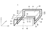
- FIG. 2 is a diagram showing a configuration example of the coil 1, which is one of the coils 1-1 to 1-12.
- the first wiring corresponds to the wirings 21, 22, 23, and 24 formed in the first wiring layer 41 parallel to the XY plane
- the second wiring is parallel to the XY plane. This corresponds to the wirings 11, 12, 13, 14, 15 formed in the second wiring layer 42.
- the opposite-side wiring is formed in the same wiring layer.
- the vias 31 to 38 are conductive wires that connect one end of the first wiring to one end of the second wiring.
- a plurality of thin lines 40 parallel to the extending direction of each wiring or via are virtual lines for making the layer structure of the coil 1 easy to see.
- the coil 1 has a single winding configuration with the coil end 51 and the coil end 52 as both ends.
- the other end of the wiring 11 having the coil end 51 as one end is connected to one end of the wiring 21 through the via 31.
- the other end of the wiring 21 is connected to one end of the wiring 12 through the via 32.
- the other end of the wiring 12 is connected to one end of the wiring 22 through the via 33.
- the other end of the wiring 22 is connected to one end of the wiring 13 through the via 34.
- the other end of the wiring 13 is connected to one end of the wiring 23 through the via 35.
- One end of the wiring 23 is connected to one end of the wiring 14 through the via 36.
- the other end of the wiring 14 is connected to one end of the wiring 24 through the via 37.
- the other end of the wiring 24 is connected to one end of the wiring 15 through the via 38.
- the other end of the wiring 15 is a coil end 52.
- the coil 1 is formed by alternately connecting the first wiring and the second wiring.
- a plurality of coils that partially overlap each other in the diagonal direction connecting the diagonals of the coils can be formed on the substrate 60.
- the coil 1-1 and the coil 1-7 partially overlap each other in the diagonal direction connecting the via 32 and the via 34 located at the diagonal of the coil 1-1 or the coil 1-7.
- the coil 1-2 and the coil 1-7 partially overlap each other in the diagonal direction connecting the via 31 and the via 33 that are located diagonally to the coil 1-2 or the coil 1-7.
- the other coil combinations partially overlap each other in the diagonal direction.
- the mounting density of the coils per unit area of the substrate 60 can be increased.
- the communication speed of data communication using inductive coupling between the coils can be increased between the plurality of semiconductor integrated circuits 101 arranged in the vertical direction (Z direction).
- the strength of the magnetic field is smaller at the corners on both sides of the wiring located on one side of the square coil than the central part of the wiring located on that side. Therefore, even if the adjacent coils in the diagonal direction partially overlap each other, the adjacent coils partially overlap each other in the diagonal direction (for example, between the coil 1-1 and the coil 1-7). Etc.) can be suppressed.
- each coil formed on the substrate 60 (for example, the dimensions and layer configuration of the wiring) is the same, each coil can be efficiently arranged on the substrate 60. The effect of increasing the density can be increased.
- the coils 1-7 are arranged in two diagonal directions connecting the diagonals of the coil 1-7. 1-7 partially overlaps each of the four coils 1-1, 1-2, 1-4, and 1-5.
- the two diagonal directions connecting the diagonals of the coil 1-7 include the first diagonal direction connecting the via 32 and the via 34 in the coil 1-7, and the via 31 and the via 33 in the coil 1-7. It is the 2nd diagonal direction to connect.
- the coil 1-5 is a self-coil and the coils 1-7, 1-8, 1-10, 1-11 are other coils
- two diagonal directions connecting the diagonals of the coil 1-5 The coil 1-5 partially overlaps each of the four coils 1-7, 1-8, 1-10, 1-11.
- the two diagonal directions connecting the diagonal of the coil 1-5 are the first diagonal direction connecting the via 32 and the via 34 in the coil 1-5, and the via 31 and the via 33 in the coil 1-5. It is the 2nd diagonal direction to connect.
- the diagonal relationship between the own coil and the other coil is the same for the other coils.
- each coil is at least active by switching between an active coil used for communication (Active Channel) and an inactive coil not used for communication (Inactive Channel). Crosstalk between coils can be suppressed.
- FIG. 3 exemplifies switching of coils used for communication at four phase timings ⁇ .
- FIG. 3 32 squares drawn at each phase timing ⁇ are simplified representations of one coil 1 shown in FIGS. 1 and 2, and partially overlap in the diagonal direction. This shows a coil arranged in a line. Eight active coils are selected at each phase timing.
- the coil 1a which is one of the 32 coils 1, will be described as a self-coil.
- the coil 1a is used for communication, and the other coils 1b and 1c arranged at positions not overlapping with the coil 1a in the diagonal direction connecting the diagonals of the coil 1a are used for communication.
- the first mode to be used is executed.
- the coil 1a is not used for communication, and is arranged at a position partially overlapping with the coil 1a in the diagonal direction connecting one diagonal of the coil 1a.
- a second mode in which the other coils 1d and 1e are used for communication is executed.
- the third mode is executed in which the coil 1a is not used for communication and the other coils 1f, 1g, and 1h having opposite sides facing the side of the coil 1a are used for communication. Is done.
- the coil 1a is not used for communication, and is arranged at a position partially overlapping with the coil 1a in the diagonal direction connecting the other diagonal of the coil 1a.
- a fourth mode in which the other coils 1i and 1j are used for communication is executed.
- a plurality of coils partially overlapping each other in the diagonal direction connecting the diagonals of the coils can be formed on the substrate 60, as many coils as possible can be arranged in a relatively narrow region.
- a relatively narrow region for example, in a memory chip, it overlaps partially in a diagonal direction in a relatively narrow area around the memory array area (for example, a peripheral area where an input / output circuit for inputting / outputting signals to / from the memory array is arranged).
- a plurality of coils arranged in parallel can be arranged.
- FIG. 4 is a diagram showing a configuration example of a DRAM chip which is an example of a memory chip.
- a plurality of coils 100 coils in the case of FIG. 4
- 100 squares drawn in the peripheral area 71 are simplified representations of the coil 1 shown in FIGS.
- 92 coils for data transmission and 8 coils for clock CLK transmission are arranged in the peripheral area 71.
- the breakdown of the 92 coils for data transmission consists of 64 coils for data signal (DQ signal) transmission, 8 coils for DMI, and 8 coils for data strobe signal (DQS signal) transmission. And 12 coils for CA.
- Quadrants A, B, C, and D represent memory cell areas.
- FIG. 5 is a diagram illustrating a configuration example of a stacked circuit 201 formed by stacking a plurality of chips.
- the stacked circuit 201 is configured by stacking a control chip 81 and memory chips 82 and 83. Inter-chip communication is performed between these chips by inductive coupling using coils 1 (see FIG. 2) respectively formed on these chips.
- Each of the control chip 81 and the memory chips 82 and 83 is an example of a semiconductor integrated circuit.
- the control chip 81 has a reception coil 92 and a transmission coil 91 disposed inside the reception coil 92.
- the transmission coil 91 is similar to the reception coil 92 at a predetermined reduction ratio so as to be disposed inside the reception coil 92. If the receiving coil 92 is a certain one coil shown in FIG. 1, although not shown in FIG. 1, the transmitting coil 91 is a coil disposed inside the certain one coil. The same applies to the transmission coil 91 and the reception coil 92 of the memory chips 82 and 83, respectively.
- the transmission coil 91 of the control chip 81, the reception coil 92 of the control chip 81, the transmission coil 91 of the memory chip 82, the reception coil 92 of the memory chip 82, the transmission coil 91 of the memory chip 83, and the reception coil 92 of the memory chip 83 are mutually connected. It is arranged at a distance that allows inductive coupling.
- control chip 81 has a transmission coil 111 for clock CLK transmission.
- Each of the memory chips 82 and 83 has a receiving coil 113 for clock CLK transmission.
- the transmission coil 111 of the control chip 81, the reception coil 113 of the memory chip 82, and the reception coil 113 of the memory chip 83 are arranged at a distance that can be inductively coupled to each other.
- the transmission coil 111 or the reception coil 113 may be a coil having a wiring structure formed in a multilayer as shown in FIG. 1 or a coil having a wiring structure formed in a single layer.
- parallel data taken out from each DRAM 112 is converted into serial data by the Ser / Des circuit 95 at 8: 1.
- the transmitter 93 uses the transmission coil 91 to transfer the converted serial data to the reception coil 92 included in a chip different from the own chip.
- the 4-phase clock CLK for data transfer is generated by the CPU 96 and the clock circuit 97 of the control chip 81.
- the transmitter 114 transfers the clock CLK generated by the control chip 81 to the reception coils 113 of the memory chips 82 and 83 by the transmission coil 111 of the control chip 81.
- the clock CLK transferred to the receiving coil 113 of each of the memory chips 82 and 83 is transmitted to the Ser / Des circuit 95 via the receiver 99. Therefore, generation of the clock CLK in the memory chips 82 and 83 is not necessary.
- a reception error may occur in the receiver 94 (see FIG. 5) connected to the self coil due to crosstalk received from other coils around the self coil when the self coil is not transmitting or receiving. Conceivable. If the receiver 94 is powered off in accordance with the phase ⁇ , the received data cannot be retained. In order to prevent reception errors due to crosstalk when the coil is not communicating while holding the data, the reception sensitivity of the receiver 94 (the detection threshold of the reception signal obtained from the reception coil) is adjusted according to the phase ⁇ .
- a threshold controller 98 is preferably provided. The threshold controller 98 is provided in each of the control chip 81 and the memory chips 82 and 83.
- FIG. 6 shows an example of the configuration of the threshold controller 98 that adjusts the hysteresis of the detection threshold V TH of the receiver 94 in accordance with the phase ⁇ .
- the threshold controller 98 controls the detection threshold V TH of the received signal obtained from the receiving coil that ends and starts to be used for communication according to the timing at which the use of the receiving coil for the communication ends and starts. It is an example.
- FIG. 7 is a diagram for explaining an example of the control operation of the detection threshold V TH by the threshold controller 98.
- the threshold controller 98 increases the absolute value of the detection threshold V TH to reduce the reception sensitivity of the receiver 94 in order to prevent reception errors of the receiver 94 connected to the coil (Noise Victim).
- the threshold controller 98 controls each mode so that the first mode, the second mode, the third mode, and the fourth mode are repeated in this order.
- the timing at which the absolute value of the noise amplitude Vnoise is maximized can be separated as much as possible from the timing at which one coil (Noise Victim) receives a signal. As a result, it is possible to reliably prevent a reception error of a receiver connected to one coil (Noise Victim).
- the threshold controller 98 is a period in which the control signal V PDM of FIG. 6 generated based on three clocks CLK ⁇ / 2 , CLK ⁇ , and CLK 3 ⁇ / 2 having different phases ⁇ is fixed at a high level (see FIG. 7). ) Increase the absolute value of the detection threshold V TH to lower the reception sensitivity of the receiver 94.
- NOR circuit 121 and 124 a logic circuit obtained by combining the AND circuit 122 and the delay circuit 123, three clocks CLK ⁇ / 2, CLK ⁇ , on the basis of the CLK 3 [pi] / 2, and generates a control signal V PDM.
- the receiver 94 is a comparator having hysteresis due to a cross-coupled NMOS transistor and a PMOS transistor Mp.
- the threshold controller 98 is connected to the output of the receiver 94 and holds the output data of the receiver 94.
- the hysteresis becomes strong while the output data of the receiver 94 is held, so that the output data of the receiver 94 can be protected from the noise amplitude Vnoise.
- the threshold controller 98 returns the detection threshold V TH to the original value.
- the integrated circuit and the laminated circuit including the integrated circuit have been described according to the embodiments.
- the present invention is not limited to the above embodiments.
- Various modifications and improvements, such as combinations and substitutions with some or all of the other embodiments, are possible within the scope of the present invention.
- the number of turns of the coil may be singular or plural.
- the position of the coil end which is an edge part of a coil is arbitrary.
- the shape of the coil may be square, rectangular or parallelogram.
- the number of other coils having corners partially overlapping with the own coil in the diagonal direction may be any number of 1, 2, 3, 4, or may be a number of 5 or more.
- the first to fourth modes are exemplified, but the mode types are not limited to these four modes.
- the number of modes may be determined according to the number of other coils having corner portions that partially overlap the own coil in a diagonal direction.
Landscapes
- Engineering & Computer Science (AREA)
- Power Engineering (AREA)
- Computer Networks & Wireless Communication (AREA)
- Signal Processing (AREA)
- Computer Hardware Design (AREA)
- Physics & Mathematics (AREA)
- Microelectronics & Electronic Packaging (AREA)
- Computing Systems (AREA)
- General Engineering & Computer Science (AREA)
- Mathematical Physics (AREA)
- Semiconductor Integrated Circuits (AREA)
- Coils Or Transformers For Communication (AREA)
- Near-Field Transmission Systems (AREA)
Abstract
Description
互いに直交するように互いに異なる層に形成された第1配線と第2配線とが交互に接続された、方形状のコイルを複数備え、
前記コイルは、前記コイルの対角を結ぶ対角方向で互いに部分的に重複する、集積回路が提供される。
11,12,13,14,15 第1配線
21,22,23,24 第2配線
31,32,33,34,35,36,37 ビア
40 仮想線
41 第1配線層
42 第2配線層
51,52 コイル端
60 基板
71 周辺領域
81 制御チップ
82,83 チップ
98 閾値コントローラ
101 半導体集積回路
121,124 NOR回路
122 AND回路
123 遅延回路
201 積層回路
Claims (9)
- 互いに直交するように互いに異なる層に形成された第1配線と第2配線とが交互に接続された、方形状のコイルを複数備え、
前記コイルは、前記コイルの対角を結ぶ対角方向で互いに部分的に重複する、集積回路。 - 前記コイルの構造は、互いに同一である、請求項1に記載の集積回路。
- 前記コイルのうちの一つである自コイルは、前記自コイルの対角を結ぶ2つの対角方向で、前記コイルのうちの他コイルと部分的に重複する、請求項1に記載の集積回路。
- 前記コイルを通信に使用するか否かが位相タイミングに応じて切り替わる、請求項1に記載の集積回路。
- 前記コイルのうちの一つである自コイルを通信に使用し、且つ、前記自コイルの対角を結ぶ対角方向で前記自コイルに重複しない位置に配置された他コイルを通信に使用するモードと、
前記自コイルを通信に使用せず、且つ、前記自コイルの対角を結ぶ対角方向で前記自コイルと部分的に重複する位置に配置された他コイルを通信に使用するモードと、
前記自コイルを通信に使用せず、且つ、前記自コイルの辺に対向する対向辺を有する他コイルを通信に使用するモードとが、前記位相タイミングに応じて切り替わる、請求項4に記載の集積回路。 - 前記コイルのうちの一つである自コイルを通信に使用し、且つ、前記自コイルの対角を結ぶ対角方向で前記自コイルに重複しない位置に配置された他コイルを通信に使用する第1モードと、
前記自コイルを通信に使用せず、且つ、前記自コイルの一方の対角を結ぶ対角方向で前記自コイルと部分的に重複する位置に配置された他コイルを通信に使用する第2モードと、
前記自コイルを通信に使用せず、且つ、前記自コイルの辺に対向する対向辺を有する他コイルを通信に使用する第3モードと、
前記自コイルを通信に使用せず、且つ、前記自コイルの他方の対角を結ぶ対角方向で前記自コイルと部分的に重複する位置に配置された他コイルを通信に使用する第4モードとが、前記位相タイミングに応じて切り替わる、請求項4に記載の集積回路。 - 前記第1モード、前記第2モード、前記第3モード、前記第4モードが、この順番で繰り返される、請求項6に記載の集積回路。
- 前記コイルの通信への使用が終了及び開始するタイミングに応じて、通信への使用が終了及び開始する該コイルから得られる受信信号の検出閾値を制御する閾値制御回路を備える、請求項4に記載の集積回路。
- 請求項1に記載の集積回路が複数積層され、
前記集積回路の一方が有する前記コイルと、前記集積回路の他方が有する前記コイルとの間の誘導結合によって、前記集積回路の一方と前記集積回路の他方との間の通信が行われる、積層回路。
Priority Applications (2)
| Application Number | Priority Date | Filing Date | Title |
|---|---|---|---|
| KR1020167002407A KR102317164B1 (ko) | 2013-11-21 | 2014-11-11 | 집적 회로 및 이를 구비한 적층 회로 |
| US14/905,406 US9749020B2 (en) | 2013-11-21 | 2014-11-11 | Integrated circuit and layered circuit provided therewith |
Applications Claiming Priority (2)
| Application Number | Priority Date | Filing Date | Title |
|---|---|---|---|
| JP2013-241386 | 2013-11-21 | ||
| JP2013241386A JP6138032B2 (ja) | 2013-11-21 | 2013-11-21 | 集積回路及びそれを備える積層回路 |
Publications (1)
| Publication Number | Publication Date |
|---|---|
| WO2015076153A1 true WO2015076153A1 (ja) | 2015-05-28 |
Family
ID=53179420
Family Applications (1)
| Application Number | Title | Priority Date | Filing Date |
|---|---|---|---|
| PCT/JP2014/079830 Ceased WO2015076153A1 (ja) | 2013-11-21 | 2014-11-11 | 集積回路及びそれを備える積層回路 |
Country Status (4)
| Country | Link |
|---|---|
| US (1) | US9749020B2 (ja) |
| JP (1) | JP6138032B2 (ja) |
| KR (1) | KR102317164B1 (ja) |
| WO (1) | WO2015076153A1 (ja) |
Cited By (3)
| Publication number | Priority date | Publication date | Assignee | Title |
|---|---|---|---|---|
| WO2020213489A1 (ja) * | 2019-04-15 | 2020-10-22 | 学校法人慶應義塾 | 通信回路、及び通信方法 |
| JP2021513738A (ja) * | 2018-02-07 | 2021-05-27 | インターナショナル・ビジネス・マシーンズ・コーポレーションInternational Business Machines Corporation | 電子回路の入力ポートを保護するための静電気保護デバイスおよび集積回路 |
| WO2026018508A1 (ja) * | 2024-07-16 | 2026-01-22 | 先端システム技術研究組合 | 半導体モジュール |
Families Citing this family (7)
| Publication number | Priority date | Publication date | Assignee | Title |
|---|---|---|---|---|
| KR20160037652A (ko) * | 2014-09-29 | 2016-04-06 | 엘지이노텍 주식회사 | 무선 전력 송신 장치 및 무선 전력 수신 장치 |
| US10062494B2 (en) * | 2014-11-03 | 2018-08-28 | Qorvo Us, Inc. | Apparatus with 3D inductors |
| CN109075446B (zh) * | 2016-01-29 | 2020-09-08 | 夏普株式会社 | 天线设备 |
| JP6683366B2 (ja) * | 2016-02-03 | 2020-04-22 | 学校法人慶應義塾 | 半導体集積回路装置 |
| US10043745B2 (en) * | 2016-04-01 | 2018-08-07 | Taiwan Semiconductor Manufacturing Company Ltd. | Semiconductor package devices integrated with inductor |
| US10027381B2 (en) * | 2016-07-27 | 2018-07-17 | Micron Technology, Inc. | Method and apparatus for inductive coupling signal transmission |
| EP4287458A4 (en) | 2021-05-21 | 2025-05-14 | Samsung Electronics Co., Ltd. | Coil for detecting foreign material, and wireless power transmitter comprising same |
Citations (5)
| Publication number | Priority date | Publication date | Assignee | Title |
|---|---|---|---|---|
| JP2004229406A (ja) * | 2003-01-23 | 2004-08-12 | Sony Corp | 分離トランス装置 |
| WO2006117834A1 (ja) * | 2005-04-25 | 2006-11-09 | Renesas Technology Corp. | 半導体装置及びicカード |
| WO2009139372A1 (ja) * | 2008-05-14 | 2009-11-19 | 学校法人 慶應義塾 | インダクタ素子、集積回路装置、及び、三次元実装回路装置 |
| JP2011233956A (ja) * | 2010-04-23 | 2011-11-17 | Renesas Electronics Corp | 電子部品及び信号伝達方法 |
| JP2012209769A (ja) * | 2011-03-30 | 2012-10-25 | Keio Gijuku | 積層集積回路装置 |
Family Cites Families (7)
| Publication number | Priority date | Publication date | Assignee | Title |
|---|---|---|---|---|
| US5394087A (en) * | 1993-08-11 | 1995-02-28 | Picker International, Inc. | Multiple quadrature surface coil system for simultaneous imaging in magnetic resonance systems |
| US6771919B2 (en) * | 2001-07-18 | 2004-08-03 | Ricoh Company, Ltd. | Image forming apparatus with reduced variation of rotation speed of image carrier |
| JP4131544B2 (ja) | 2004-02-13 | 2008-08-13 | 学校法人慶應義塾 | 電子回路 |
| DE102005051059B4 (de) * | 2005-10-25 | 2016-09-15 | Maxon Motor Ag | Verfahren zur Herstellung eines Elektromotors und Elektromotor mit mehrlagigen rautenartigen Einzelspulen aus Draht |
| US8169185B2 (en) * | 2006-01-31 | 2012-05-01 | Mojo Mobility, Inc. | System and method for inductive charging of portable devices |
| JP2009081943A (ja) * | 2007-09-26 | 2009-04-16 | Seiko Epson Corp | 送電制御装置、送電装置、送電側装置および無接点電力伝送システム |
| JP5247367B2 (ja) * | 2008-11-13 | 2013-07-24 | ルネサスエレクトロニクス株式会社 | Rf電力増幅器 |
-
2013
- 2013-11-21 JP JP2013241386A patent/JP6138032B2/ja active Active
-
2014
- 2014-11-11 WO PCT/JP2014/079830 patent/WO2015076153A1/ja not_active Ceased
- 2014-11-11 KR KR1020167002407A patent/KR102317164B1/ko active Active
- 2014-11-11 US US14/905,406 patent/US9749020B2/en active Active
Patent Citations (5)
| Publication number | Priority date | Publication date | Assignee | Title |
|---|---|---|---|---|
| JP2004229406A (ja) * | 2003-01-23 | 2004-08-12 | Sony Corp | 分離トランス装置 |
| WO2006117834A1 (ja) * | 2005-04-25 | 2006-11-09 | Renesas Technology Corp. | 半導体装置及びicカード |
| WO2009139372A1 (ja) * | 2008-05-14 | 2009-11-19 | 学校法人 慶應義塾 | インダクタ素子、集積回路装置、及び、三次元実装回路装置 |
| JP2011233956A (ja) * | 2010-04-23 | 2011-11-17 | Renesas Electronics Corp | 電子部品及び信号伝達方法 |
| JP2012209769A (ja) * | 2011-03-30 | 2012-10-25 | Keio Gijuku | 積層集積回路装置 |
Non-Patent Citations (1)
| Title |
|---|
| NORIYUKI MIURA ET AL.: "Low- Power and Wideband Inductive-Coupling Communication for 3D Integration", JOURNAL OF JAPAN INSTITUTE OF ELECTRONICS PACKAGING, vol. 11, 1 May 2008 (2008-05-01), RENSHI SAWADA, pages 174 - 181 * |
Cited By (6)
| Publication number | Priority date | Publication date | Assignee | Title |
|---|---|---|---|---|
| JP2021513738A (ja) * | 2018-02-07 | 2021-05-27 | インターナショナル・ビジネス・マシーンズ・コーポレーションInternational Business Machines Corporation | 電子回路の入力ポートを保護するための静電気保護デバイスおよび集積回路 |
| JP7189958B2 (ja) | 2018-02-07 | 2022-12-14 | インターナショナル・ビジネス・マシーンズ・コーポレーション | 電子回路の入力ポートを保護するための静電気保護デバイスおよび集積回路 |
| WO2020213489A1 (ja) * | 2019-04-15 | 2020-10-22 | 学校法人慶應義塾 | 通信回路、及び通信方法 |
| JPWO2020213489A1 (ja) * | 2019-04-15 | 2020-10-22 | ||
| JP7320861B2 (ja) | 2019-04-15 | 2023-08-04 | 慶應義塾 | 通信回路、及び通信方法 |
| WO2026018508A1 (ja) * | 2024-07-16 | 2026-01-22 | 先端システム技術研究組合 | 半導体モジュール |
Also Published As
| Publication number | Publication date |
|---|---|
| KR20160088851A (ko) | 2016-07-26 |
| KR102317164B1 (ko) | 2021-10-22 |
| US9749020B2 (en) | 2017-08-29 |
| JP6138032B2 (ja) | 2017-05-31 |
| JP2015103584A (ja) | 2015-06-04 |
| US20160156390A1 (en) | 2016-06-02 |
Similar Documents
| Publication | Publication Date | Title |
|---|---|---|
| JP6138032B2 (ja) | 集積回路及びそれを備える積層回路 | |
| TWI587654B (zh) | Directional coupling communication device | |
| JP5280880B2 (ja) | 半導体集積回路装置 | |
| US9053950B2 (en) | Electronic circuit | |
| US8964483B2 (en) | Semiconductor device and memory system | |
| JP4860637B2 (ja) | 信号伝送方式及び半導体集積回路装置 | |
| JP4977101B2 (ja) | 積層型半導体装置 | |
| JP5229213B2 (ja) | インダクタ結合を用いて信号伝送を行う半導体装置 | |
| TW201429087A (zh) | 記憶卡轉接器 | |
| KR20200135165A (ko) | 다이들에 대한 인터커넥트 허브 | |
| KR20110016878A (ko) | 인덕터 소자, 집적 회로 장치, 및 삼차원 실장 회로 장치 | |
| JP2006294824A (ja) | 積層型半導体装置 | |
| US11437350B2 (en) | Semiconductor device | |
| JP5791326B2 (ja) | 積層集積回路装置 | |
| US9431372B2 (en) | Multi-chip package | |
| US20100078211A1 (en) | Memory module and topology of circuit board | |
| US12444700B2 (en) | Semiconductor device, semiconductor package, and memory system | |
| US11810852B2 (en) | Module substrate for semiconductor module and semoconductor memory module | |
| US9570383B2 (en) | Semiconductor package, module substrate and semiconductor package module having the same | |
| JP7493267B2 (ja) | 通信装置 | |
| US8912656B2 (en) | Integrated circuit package and physical layer interface arrangement | |
| JP2023179947A (ja) | メモリー基板 | |
| JP2015069658A (ja) | メモリ |
Legal Events
| Date | Code | Title | Description |
|---|---|---|---|
| 121 | Ep: the epo has been informed by wipo that ep was designated in this application |
Ref document number: 14864247 Country of ref document: EP Kind code of ref document: A1 |
|
| WWE | Wipo information: entry into national phase |
Ref document number: 14905406 Country of ref document: US |
|
| ENP | Entry into the national phase |
Ref document number: 20167002407 Country of ref document: KR Kind code of ref document: A |
|
| NENP | Non-entry into the national phase |
Ref country code: DE |
|
| 122 | Ep: pct application non-entry in european phase |
Ref document number: 14864247 Country of ref document: EP Kind code of ref document: A1 |