WO2015068458A1 - GaNテンプレート基板およびデバイス基板 - Google Patents
GaNテンプレート基板およびデバイス基板 Download PDFInfo
- Publication number
- WO2015068458A1 WO2015068458A1 PCT/JP2014/073488 JP2014073488W WO2015068458A1 WO 2015068458 A1 WO2015068458 A1 WO 2015068458A1 JP 2014073488 W JP2014073488 W JP 2014073488W WO 2015068458 A1 WO2015068458 A1 WO 2015068458A1
- Authority
- WO
- WIPO (PCT)
- Prior art keywords
- gan
- layer
- substrate
- gan layer
- template substrate
- Prior art date
- Legal status (The legal status is an assumption and is not a legal conclusion. Google has not performed a legal analysis and makes no representation as to the accuracy of the status listed.)
- Ceased
Links
Images
Classifications
-
- H—ELECTRICITY
- H10—SEMICONDUCTOR DEVICES; ELECTRIC SOLID-STATE DEVICES NOT OTHERWISE PROVIDED FOR
- H10H—INORGANIC LIGHT-EMITTING SEMICONDUCTOR DEVICES HAVING POTENTIAL BARRIERS
- H10H20/00—Individual inorganic light-emitting semiconductor devices having potential barriers, e.g. light-emitting diodes [LED]
- H10H20/80—Constructional details
- H10H20/81—Bodies
- H10H20/815—Bodies having stress relaxation structures, e.g. buffer layers
-
- C—CHEMISTRY; METALLURGY
- C30—CRYSTAL GROWTH
- C30B—SINGLE-CRYSTAL GROWTH; UNIDIRECTIONAL SOLIDIFICATION OF EUTECTIC MATERIAL OR UNIDIRECTIONAL DEMIXING OF EUTECTOID MATERIAL; REFINING BY ZONE-MELTING OF MATERIAL; PRODUCTION OF A HOMOGENEOUS POLYCRYSTALLINE MATERIAL WITH DEFINED STRUCTURE; SINGLE CRYSTALS OR HOMOGENEOUS POLYCRYSTALLINE MATERIAL WITH DEFINED STRUCTURE; AFTER-TREATMENT OF SINGLE CRYSTALS OR A HOMOGENEOUS POLYCRYSTALLINE MATERIAL WITH DEFINED STRUCTURE; APPARATUS THEREFOR
- C30B19/00—Liquid-phase epitaxial-layer growth
- C30B19/02—Liquid-phase epitaxial-layer growth using molten solvents, e.g. flux
-
- C—CHEMISTRY; METALLURGY
- C30—CRYSTAL GROWTH
- C30B—SINGLE-CRYSTAL GROWTH; UNIDIRECTIONAL SOLIDIFICATION OF EUTECTIC MATERIAL OR UNIDIRECTIONAL DEMIXING OF EUTECTOID MATERIAL; REFINING BY ZONE-MELTING OF MATERIAL; PRODUCTION OF A HOMOGENEOUS POLYCRYSTALLINE MATERIAL WITH DEFINED STRUCTURE; SINGLE CRYSTALS OR HOMOGENEOUS POLYCRYSTALLINE MATERIAL WITH DEFINED STRUCTURE; AFTER-TREATMENT OF SINGLE CRYSTALS OR A HOMOGENEOUS POLYCRYSTALLINE MATERIAL WITH DEFINED STRUCTURE; APPARATUS THEREFOR
- C30B19/00—Liquid-phase epitaxial-layer growth
- C30B19/12—Liquid-phase epitaxial-layer growth characterised by the substrate
-
- C—CHEMISTRY; METALLURGY
- C30—CRYSTAL GROWTH
- C30B—SINGLE-CRYSTAL GROWTH; UNIDIRECTIONAL SOLIDIFICATION OF EUTECTIC MATERIAL OR UNIDIRECTIONAL DEMIXING OF EUTECTOID MATERIAL; REFINING BY ZONE-MELTING OF MATERIAL; PRODUCTION OF A HOMOGENEOUS POLYCRYSTALLINE MATERIAL WITH DEFINED STRUCTURE; SINGLE CRYSTALS OR HOMOGENEOUS POLYCRYSTALLINE MATERIAL WITH DEFINED STRUCTURE; AFTER-TREATMENT OF SINGLE CRYSTALS OR A HOMOGENEOUS POLYCRYSTALLINE MATERIAL WITH DEFINED STRUCTURE; APPARATUS THEREFOR
- C30B25/00—Single-crystal growth by chemical reaction of reactive gases, e.g. chemical vapour-deposition growth
- C30B25/02—Epitaxial-layer growth
-
- C—CHEMISTRY; METALLURGY
- C30—CRYSTAL GROWTH
- C30B—SINGLE-CRYSTAL GROWTH; UNIDIRECTIONAL SOLIDIFICATION OF EUTECTIC MATERIAL OR UNIDIRECTIONAL DEMIXING OF EUTECTOID MATERIAL; REFINING BY ZONE-MELTING OF MATERIAL; PRODUCTION OF A HOMOGENEOUS POLYCRYSTALLINE MATERIAL WITH DEFINED STRUCTURE; SINGLE CRYSTALS OR HOMOGENEOUS POLYCRYSTALLINE MATERIAL WITH DEFINED STRUCTURE; AFTER-TREATMENT OF SINGLE CRYSTALS OR A HOMOGENEOUS POLYCRYSTALLINE MATERIAL WITH DEFINED STRUCTURE; APPARATUS THEREFOR
- C30B29/00—Single crystals or homogeneous polycrystalline material with defined structure characterised by the material or by their shape
- C30B29/10—Inorganic compounds or compositions
- C30B29/40—AIIIBV compounds wherein A is B, Al, Ga, In or Tl and B is N, P, As, Sb or Bi
- C30B29/403—AIII-nitrides
- C30B29/406—Gallium nitride
-
- C—CHEMISTRY; METALLURGY
- C30—CRYSTAL GROWTH
- C30B—SINGLE-CRYSTAL GROWTH; UNIDIRECTIONAL SOLIDIFICATION OF EUTECTIC MATERIAL OR UNIDIRECTIONAL DEMIXING OF EUTECTOID MATERIAL; REFINING BY ZONE-MELTING OF MATERIAL; PRODUCTION OF A HOMOGENEOUS POLYCRYSTALLINE MATERIAL WITH DEFINED STRUCTURE; SINGLE CRYSTALS OR HOMOGENEOUS POLYCRYSTALLINE MATERIAL WITH DEFINED STRUCTURE; AFTER-TREATMENT OF SINGLE CRYSTALS OR A HOMOGENEOUS POLYCRYSTALLINE MATERIAL WITH DEFINED STRUCTURE; APPARATUS THEREFOR
- C30B29/00—Single crystals or homogeneous polycrystalline material with defined structure characterised by the material or by their shape
- C30B29/60—Single crystals or homogeneous polycrystalline material with defined structure characterised by the material or by their shape characterised by shape
- C30B29/68—Crystals with laminate structure, e.g. "superlattices"
-
- C—CHEMISTRY; METALLURGY
- C30—CRYSTAL GROWTH
- C30B—SINGLE-CRYSTAL GROWTH; UNIDIRECTIONAL SOLIDIFICATION OF EUTECTIC MATERIAL OR UNIDIRECTIONAL DEMIXING OF EUTECTOID MATERIAL; REFINING BY ZONE-MELTING OF MATERIAL; PRODUCTION OF A HOMOGENEOUS POLYCRYSTALLINE MATERIAL WITH DEFINED STRUCTURE; SINGLE CRYSTALS OR HOMOGENEOUS POLYCRYSTALLINE MATERIAL WITH DEFINED STRUCTURE; AFTER-TREATMENT OF SINGLE CRYSTALS OR A HOMOGENEOUS POLYCRYSTALLINE MATERIAL WITH DEFINED STRUCTURE; APPARATUS THEREFOR
- C30B9/00—Single-crystal growth from melt solutions using molten solvents
- C30B9/04—Single-crystal growth from melt solutions using molten solvents by cooling of the solution
- C30B9/08—Single-crystal growth from melt solutions using molten solvents by cooling of the solution using other solvents
- C30B9/10—Metal solvents
-
- H—ELECTRICITY
- H10—SEMICONDUCTOR DEVICES; ELECTRIC SOLID-STATE DEVICES NOT OTHERWISE PROVIDED FOR
- H10D—INORGANIC ELECTRIC SEMICONDUCTOR DEVICES
- H10D30/00—Field-effect transistors [FET]
- H10D30/01—Manufacture or treatment
- H10D30/015—Manufacture or treatment of FETs having heterojunction interface channels or heterojunction gate electrodes, e.g. HEMT
-
- H—ELECTRICITY
- H10—SEMICONDUCTOR DEVICES; ELECTRIC SOLID-STATE DEVICES NOT OTHERWISE PROVIDED FOR
- H10D—INORGANIC ELECTRIC SEMICONDUCTOR DEVICES
- H10D30/00—Field-effect transistors [FET]
- H10D30/40—FETs having zero-dimensional [0D], one-dimensional [1D] or two-dimensional [2D] charge carrier gas channels
- H10D30/47—FETs having zero-dimensional [0D], one-dimensional [1D] or two-dimensional [2D] charge carrier gas channels having two-dimensional [2D] charge carrier gas channels, e.g. nanoribbon FETs or high electron mobility transistors [HEMT]
- H10D30/471—High electron mobility transistors [HEMT] or high hole mobility transistors [HHMT]
- H10D30/475—High electron mobility transistors [HEMT] or high hole mobility transistors [HHMT] having wider bandgap layer formed on top of lower bandgap active layer, e.g. undoped barrier HEMTs such as i-AlGaN/GaN HEMTs
- H10D30/4755—High electron mobility transistors [HEMT] or high hole mobility transistors [HHMT] having wider bandgap layer formed on top of lower bandgap active layer, e.g. undoped barrier HEMTs such as i-AlGaN/GaN HEMTs having wide bandgap charge-carrier supplying layers, e.g. modulation doped HEMTs such as n-AlGaAs/GaAs HEMTs
-
- H—ELECTRICITY
- H10—SEMICONDUCTOR DEVICES; ELECTRIC SOLID-STATE DEVICES NOT OTHERWISE PROVIDED FOR
- H10H—INORGANIC LIGHT-EMITTING SEMICONDUCTOR DEVICES HAVING POTENTIAL BARRIERS
- H10H20/00—Individual inorganic light-emitting semiconductor devices having potential barriers, e.g. light-emitting diodes [LED]
- H10H20/01—Manufacture or treatment
- H10H20/011—Manufacture or treatment of bodies, e.g. forming semiconductor layers
- H10H20/013—Manufacture or treatment of bodies, e.g. forming semiconductor layers having light-emitting regions comprising only Group III-V materials
- H10H20/0133—Manufacture or treatment of bodies, e.g. forming semiconductor layers having light-emitting regions comprising only Group III-V materials with a substrate not being Group III-V materials
- H10H20/01335—Manufacture or treatment of bodies, e.g. forming semiconductor layers having light-emitting regions comprising only Group III-V materials with a substrate not being Group III-V materials the light-emitting regions comprising nitride materials
-
- H—ELECTRICITY
- H10—SEMICONDUCTOR DEVICES; ELECTRIC SOLID-STATE DEVICES NOT OTHERWISE PROVIDED FOR
- H10H—INORGANIC LIGHT-EMITTING SEMICONDUCTOR DEVICES HAVING POTENTIAL BARRIERS
- H10H20/00—Individual inorganic light-emitting semiconductor devices having potential barriers, e.g. light-emitting diodes [LED]
- H10H20/01—Manufacture or treatment
- H10H20/011—Manufacture or treatment of bodies, e.g. forming semiconductor layers
- H10H20/013—Manufacture or treatment of bodies, e.g. forming semiconductor layers having light-emitting regions comprising only Group III-V materials
- H10H20/0137—Manufacture or treatment of bodies, e.g. forming semiconductor layers having light-emitting regions comprising only Group III-V materials the light-emitting regions comprising nitride materials
-
- H—ELECTRICITY
- H10—SEMICONDUCTOR DEVICES; ELECTRIC SOLID-STATE DEVICES NOT OTHERWISE PROVIDED FOR
- H10H—INORGANIC LIGHT-EMITTING SEMICONDUCTOR DEVICES HAVING POTENTIAL BARRIERS
- H10H20/00—Individual inorganic light-emitting semiconductor devices having potential barriers, e.g. light-emitting diodes [LED]
- H10H20/80—Constructional details
- H10H20/81—Bodies
- H10H20/822—Materials of the light-emitting regions
- H10H20/824—Materials of the light-emitting regions comprising only Group III-V materials, e.g. GaP
- H10H20/825—Materials of the light-emitting regions comprising only Group III-V materials, e.g. GaP containing nitrogen, e.g. GaN
-
- H—ELECTRICITY
- H10—SEMICONDUCTOR DEVICES; ELECTRIC SOLID-STATE DEVICES NOT OTHERWISE PROVIDED FOR
- H10P—GENERIC PROCESSES OR APPARATUS FOR THE MANUFACTURE OR TREATMENT OF DEVICES COVERED BY CLASS H10
- H10P14/00—Formation of materials, e.g. in the shape of layers or pillars
- H10P14/20—Formation of materials, e.g. in the shape of layers or pillars of semiconductor materials
- H10P14/24—Formation of materials, e.g. in the shape of layers or pillars of semiconductor materials using chemical vapour deposition [CVD]
-
- H—ELECTRICITY
- H10—SEMICONDUCTOR DEVICES; ELECTRIC SOLID-STATE DEVICES NOT OTHERWISE PROVIDED FOR
- H10P—GENERIC PROCESSES OR APPARATUS FOR THE MANUFACTURE OR TREATMENT OF DEVICES COVERED BY CLASS H10
- H10P14/00—Formation of materials, e.g. in the shape of layers or pillars
- H10P14/20—Formation of materials, e.g. in the shape of layers or pillars of semiconductor materials
- H10P14/29—Formation of materials, e.g. in the shape of layers or pillars of semiconductor materials characterised by the substrates
- H10P14/2901—Materials
- H10P14/2921—Materials being crystalline insulating materials
-
- H—ELECTRICITY
- H10—SEMICONDUCTOR DEVICES; ELECTRIC SOLID-STATE DEVICES NOT OTHERWISE PROVIDED FOR
- H10P—GENERIC PROCESSES OR APPARATUS FOR THE MANUFACTURE OR TREATMENT OF DEVICES COVERED BY CLASS H10
- H10P14/00—Formation of materials, e.g. in the shape of layers or pillars
- H10P14/20—Formation of materials, e.g. in the shape of layers or pillars of semiconductor materials
- H10P14/32—Formation of materials, e.g. in the shape of layers or pillars of semiconductor materials characterised by intermediate layers between substrates and deposited layers
- H10P14/3202—Materials thereof
- H10P14/3214—Materials thereof being Group IIIA-VA semiconductors
- H10P14/3216—Nitrides
-
- H—ELECTRICITY
- H10—SEMICONDUCTOR DEVICES; ELECTRIC SOLID-STATE DEVICES NOT OTHERWISE PROVIDED FOR
- H10P—GENERIC PROCESSES OR APPARATUS FOR THE MANUFACTURE OR TREATMENT OF DEVICES COVERED BY CLASS H10
- H10P14/00—Formation of materials, e.g. in the shape of layers or pillars
- H10P14/20—Formation of materials, e.g. in the shape of layers or pillars of semiconductor materials
- H10P14/32—Formation of materials, e.g. in the shape of layers or pillars of semiconductor materials characterised by intermediate layers between substrates and deposited layers
- H10P14/3242—Structure
- H10P14/3244—Layer structure
- H10P14/3248—Layer structure consisting of two layers
-
- H—ELECTRICITY
- H10—SEMICONDUCTOR DEVICES; ELECTRIC SOLID-STATE DEVICES NOT OTHERWISE PROVIDED FOR
- H10P—GENERIC PROCESSES OR APPARATUS FOR THE MANUFACTURE OR TREATMENT OF DEVICES COVERED BY CLASS H10
- H10P14/00—Formation of materials, e.g. in the shape of layers or pillars
- H10P14/20—Formation of materials, e.g. in the shape of layers or pillars of semiconductor materials
- H10P14/34—Deposited materials, e.g. layers
- H10P14/3402—Deposited materials, e.g. layers characterised by the chemical composition
- H10P14/3414—Deposited materials, e.g. layers characterised by the chemical composition being group IIIA-VIA materials
- H10P14/3416—Nitrides
-
- H—ELECTRICITY
- H10—SEMICONDUCTOR DEVICES; ELECTRIC SOLID-STATE DEVICES NOT OTHERWISE PROVIDED FOR
- H10D—INORGANIC ELECTRIC SEMICONDUCTOR DEVICES
- H10D30/00—Field-effect transistors [FET]
- H10D30/40—FETs having zero-dimensional [0D], one-dimensional [1D] or two-dimensional [2D] charge carrier gas channels
- H10D30/47—FETs having zero-dimensional [0D], one-dimensional [1D] or two-dimensional [2D] charge carrier gas channels having two-dimensional [2D] charge carrier gas channels, e.g. nanoribbon FETs or high electron mobility transistors [HEMT]
-
- H—ELECTRICITY
- H10—SEMICONDUCTOR DEVICES; ELECTRIC SOLID-STATE DEVICES NOT OTHERWISE PROVIDED FOR
- H10D—INORGANIC ELECTRIC SEMICONDUCTOR DEVICES
- H10D62/00—Semiconductor bodies, or regions thereof, of devices having potential barriers
- H10D62/80—Semiconductor bodies, or regions thereof, of devices having potential barriers characterised by the materials
- H10D62/85—Semiconductor bodies, or regions thereof, of devices having potential barriers characterised by the materials being Group III-V materials, e.g. GaAs
- H10D62/8503—Nitride Group III-V materials, e.g. AlN or GaN
-
- H—ELECTRICITY
- H10—SEMICONDUCTOR DEVICES; ELECTRIC SOLID-STATE DEVICES NOT OTHERWISE PROVIDED FOR
- H10H—INORGANIC LIGHT-EMITTING SEMICONDUCTOR DEVICES HAVING POTENTIAL BARRIERS
- H10H20/00—Individual inorganic light-emitting semiconductor devices having potential barriers, e.g. light-emitting diodes [LED]
- H10H20/80—Constructional details
- H10H20/81—Bodies
- H10H20/811—Bodies having quantum effect structures or superlattices, e.g. tunnel junctions
- H10H20/812—Bodies having quantum effect structures or superlattices, e.g. tunnel junctions within the light-emitting regions, e.g. having quantum confinement structures
Definitions
- the present invention relates to a GaN template substrate formed by forming a GaN layer on a base substrate.
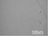
- FIG. 3 is a Nomarski differential interference microscopic image of the surface of the device substrate where such morphological abnormality has occurred.
- a line-like morphological crack (line crack) is confirmed at a point indicated by an arrow.
- the device chip formed in the morphology abnormality occurrence part is a defective product that can not exhibit the required characteristics. Therefore, the occurrence of the morphological abnormality is a factor to reduce the productivity of the device chip.
- Non-Patent Document 1 it is generally known that cracks occur, for example, when a GaN film is thickly laminated on a sapphire substrate, and in order to suppress the occurrence of such cracks, introducing a low temperature intermediate layer into the laminated structure Has already been found to be effective (see, for example, Non-Patent Document 1).
- An object of the present invention is to realize a device substrate in which no streak-like morphological abnormality occurs.
- the inventor of the present invention repeats various studies, and in the MOCVD-GaN template (seed substrate), when the GaN film has high inherent compressive stress or when the GaN film has high crystallinity. It has been found that it is possible to suppress the above-mentioned streak-like morphological abnormality.
- both compressive stress and crystallinity are values that can be quantified by Raman spectroscopy.
- a GaN template substrate includes a base substrate and a first GaN layer epitaxially formed on the base substrate, and the first GaN
- the compressive stress inherent in the in-plane direction of the layer was set to be 260 MPa or more.
- a GaN template substrate includes a base substrate and a first GaN layer epitaxially formed on the base substrate, and Raman spectroscopy of the first GaN layer is performed.
- the half width of the peak of the E 2 phonon of GaN in the vicinity of the wave number 568 nm ⁇ 1 in the Raman spectrum obtained in the above was set to 1.8 cm ⁇ 1 or less.
- a GaN template substrate includes a base substrate, and a first GaN layer epitaxially formed on the base substrate, and the in-plane direction of the first GaN layer is intrinsic Compressive stress is 260 MPa or more, and the half width of the E2 phonon peak of GaN in the vicinity of wave number 568 nm -1 in the Raman spectrum obtained by performing Raman spectroscopy measurement of the first GaN layer is 1 It was made to be .8 cm -1 or less.
- the value of the compressive stress is determined from a Raman spectrum obtained by performing Raman spectroscopy measurement of the first GaN layer. It was a thing.
- the GaN template substrate according to any one of the first to fourth aspects further comprises a second GaN layer epitaxially formed on the first GaN layer. did.
- the first GaN layer is formed by the MOCVD method
- the second GaN layer is formed by the Flux method. It was made to be formed by polishing the surface of the resulting GaN single crystal layer.
- a device substrate comprising the GaN template substrate of any of the first to fourth aspects, a second GaN layer epitaxially formed on the first GaN layer, and And a device layer of group 13 nitride epitaxially formed on the second GaN layer.
- the occurrence of streak-like morphological abnormalities on the surface of a device substrate produced using the GaN template substrate according to the present invention is suppressed, so that a device chip (LED chip, The manufacturing yield of the HEMT chip is improved.
- the manufacturing yield of the device chips (LED chips, HEMT chips) is improved.
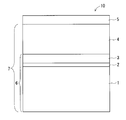
- FIG. It is a figure which shows typically the cross-section of the device board
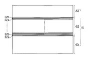
- FIG. It is a figure which illustrates the structure of the device layer 5 in the case of forming the device layer 5 as what has LED structure. It is a Nomarski-type differential interference microscope image of the device substrate surface in which the morphological abnormality has generate
- group numbers of the periodic table shown in the present specification are those of group numbers 1 to 18 according to the revised edition of Inorganic Chemical Nomenclature according to International Union of Pure Applied Chemistry (IUPAC) in 1989.
- Group 13 refers to aluminum (Al), gallium (Ga), indium (In) and the like, and group 15 refers to nitrogen (N), phosphorus (P), arsenic (As), antimony (Sb) and the like.
- FIG. 1 is a view schematically showing a cross-sectional structure of a device substrate 10 according to the embodiment of the present invention.
- Device substrate 10 includes base substrate 1, buffer layer 2, first GaN layer 3, second GaN layer 4, and device layer 5.
- the stacked structure of the base substrate 1, the buffer layer 2 and the first GaN layer 3 corresponds to the MOCVD-GaN template 6, and the stacked body of the MOCVD-GaN template 6 and the second GaN layer 4 is It corresponds to Flux-GaN template 7.
- the base substrate 1 It is preferable to use a single crystal c-plane sapphire substrate as the base substrate 1. There is no particular limitation on the size, but in terms of ease of handling, it is preferable that the diameter is about several inches and the thickness is about several hundred ⁇ m to several mm.
- the buffer layer 2 is a layer formed at a formation temperature lower than the formation temperature of the group 13 nitride crystal layer so that the group 13 nitride crystal layer of excellent crystal quality can be formed thereon.
- the buffer layer 2 can be formed of, for example, GaN.
- the buffer layer 2 is preferably formed on the base substrate 1 to a thickness of 20 nm to 100 nm by the MOCVD method.
- the first GaN layer 3 is a GaN single crystal thin film epitaxially formed on the buffer layer 2 by the MOCVD method.
- the first GaN layer 3 is preferably formed to a thickness of 1 ⁇ m to 5 ⁇ m.
- the first GaN layer 3 is formed such that the compressive stress inherent in the in-plane direction is 260 MPa or more.
- it is formed so that the half value width of the peak (Raman line) of the E 2 phonon of GaN in the vicinity of a wave number 568 nm ⁇ 1 of a Raman spectrum obtained by Raman spectroscopy measurement is 1.8 cm ⁇ 1 or less.
- the half value width of the peak is a value that is an index indicating the crystallinity of the first GaN layer 3, and the smaller the value is, the better the crystallinity of the first GaN layer 3 is. Can.
- the peak of the Raman spectrum is shifted to the high wave number side (plus side) when the measurement target contains compressive stress, and to the low wave number side (minus side) when tensile stress is present. shift.
- the value of the reference wave number representing the zero stress state is a non-strained GaN single crystal (a GaN single crystal having a spontaneous generation nucleus produced by the flux method as a growth starting point) It can be determined by performing Raman spectroscopy measurement under the same conditions as above for a crystal).
- occurrence of streak-like morphological abnormalities on the surface is preferably suppressed by satisfying at least one of the above-described requirements regarding the intrinsic stress and the half width.
- These requirements appropriately adjust the formation conditions of the first GaN layer 3, more specifically, the deposition temperature (substrate temperature), and the ratio of the hydrogen gas partial pressure to the NH 3 gas partial pressure. It is possible to realize by doing.
- the second GaN layer 4 is a GaN single crystal thin film epitaxially formed on the first GaN layer 3 by the flux method.
- the second GaN layer 4 is preferably formed to a thickness of 5 ⁇ m to 500 ⁇ m. More specifically, the second GaN layer 4 has a flat surface, for example, by polishing a GaN layer grown by Na flux (Na-Flux) method using a melt of alkali metal Na from the surface side. The thickness is adjusted as appropriate.
- polishing process grinding
- the crystal growth method employed to form the GaN single crystal layer to be the second GaN layer 4 is not necessarily the flux method.
- the HVPE method may be used, or the MOCVD method may be used.
- the device layer 5 is one or more layers of group 13 nitride which are epitaxially formed on the second GaN layer 4.
- the specific configuration of the device layer 5 may be appropriately determined depending on the structure (LED structure, HEMT structure, etc.) of the device to be manufactured.
- the device layer 5 is preferably formed by the MOCVD method, but may be formed by another crystal growth method.
- FIG. 2 is a diagram illustrating the configuration of the device layer 5 in the case where the device layer 5 is formed to have, for example, an LED structure.
- the device layer 5 shown in FIG. 2 is formed by laminating an n-type semiconductor layer 51, an active layer 52, and a p-type semiconductor layer 53 in this order.
- the n-type semiconductor layer 51 is a group 13 nitride layer doped with Si.
- the n-type semiconductor layer 51 is preferably formed of GaN to a thickness of 100 nm to 3000 nm.
- the Si concentration in the n-type semiconductor layer 51 is preferably about 1 ⁇ 10 18 / cm 3 to 1 ⁇ 10 19 / cm 3 .
- the active layer 52 is a layer to be a light emitting region in the LED element.
- the active layer 52 is a multiple quantum well layer formed by alternately and repeatedly laminating a first unit layer (well layer) 52 a and a second unit layer (barrier layer) 52 b having different compositions.
- the first unit layer 52a is formed to a thickness of 1 nm ⁇ 5 nm in In x Ga 1-x N ( 0.05 ⁇ x ⁇ 0.25)
- the second unit layer 52b is 2nm in GaN It is formed to a thickness of ⁇ 10 nm.
- the In molar ratio x in In x Ga 1 -x N is determined according to the wavelength of light to be emitted in the LED element.
- the number of repetitions of the first unit layer 52a and the second unit layer 52b is preferably 2 to 20.
- the p-type semiconductor layer 53 is a Group 13 nitride layer doped with Mg.
- the p-type semiconductor layer 53 is preferably formed of GaN to a thickness of 50 nm to 200 nm.
- the Mg concentration in the p-type semiconductor layer 53 is preferably about 5 ⁇ 10 18 / cm 3 to 1 ⁇ 10 20 / cm 3 .
- the layer formation by MOCVD is performed using an organic metal (MO) source gas (TMG (trimethylgallium), TMA (trimethylaluminum), TMI (trimethylindium), etc.) for Group 13 elements such as Ga, Al, In, and the like.
- MO organic metal
- TMG trimethylgallium
- TMA trimethylaluminum
- TMI trimethylindium
- Group 13 elements such as Ga, Al, In, and the like.
- MOCVD furnace configured to be able to supply NH 3 gas, hydrogen gas and nitrogen gas into the reactor, the organometallic raw material is heated while heating the formation target substrate placed in the reactor to a predetermined temperature It is carried out by depositing group 13 nitride crystals produced by the gas phase reaction of gas and NH 3 gas on a formation target substrate.
- the formation of the GaN layer by the Na flux method is generally performed by immersing the formation target substrate in a melt containing metal Ga, metal Na, and carbon in a growth vessel (alumina crucible) disposed horizontally rotatable in a pressure resistant vessel. This is realized by maintaining the inside of the growth container at a predetermined temperature and a predetermined pressure while introducing nitrogen gas in a state where the growth container is rotated horizontally.
- a growth vessel alumina crucible
- Examples A to I Nine types of device substrates 10 (samples A to I) having variously different conditions for forming the first GaN layer 3 were prepared and evaluated. In addition, as the device layer 5, the LED structure illustrated in FIG. 2 was formed.
- a single crystal c-plane sapphire substrate having a diameter of 4 inches and a thickness of 630 ⁇ m was prepared as the base substrate 1.
- the base substrate 1 was placed in a MOCVD furnace and heated at 1150 ° C. for 10 minutes in a hydrogen atmosphere to clean the surface.
- the substrate temperature was lowered to 500 ° C.
- TMG and NH 3 were used as raw materials
- hydrogen was used as a carrier gas
- a GaN layer as the buffer layer 2 was grown to a thickness of 30 nm by MOCVD.
- the first GaN layer 3 was grown to a thickness of 3 ⁇ m by MOCVD using TMG and NH 3 as source gases and hydrogen as a carrier gas.
- the pressure in the reactor was 100 kPa
- the group 15 / group 13 gas ratio was 2000.
- the group 15 / group 13 gas ratio is the ratio (molar ratio) of the supply amount of the group 15 raw material to the supply amount of the group 13 raw material.
- the substrate temperature at the time of forming the first GaN layer 3 and the ratio of the hydrogen gas partial pressure to the NH 3 gas partial pressure in the MOCVD reactor differed depending on the sample. Specifically, the substrate temperature was changed to three levels of 1050 ° C., 1100 ° C. and 1150 ° C.
- the gas partial pressure ratio is expressed by how many times the hydrogen gas partial pressure is the NH 3 gas partial pressure, and this is divided into three levels of three times, four times, and five times. As a result, all of the combinations of the substrate temperature and the gas partial pressure ratio at the time of forming the first GaN layer 3 are different for the samples A to I.
- the MOCVD-GaN template 6 is obtained. After the obtained MOCVD-GaN template 6 is taken out of the MOCVD furnace, the Raman stress is measured for each sample to evaluate the intrinsic stress in the first GaN layer 3 and the crystallinity of the first GaN layer 3 did.
- the device conditions at the time of the evaluation concerned are as follows.
- Light source Ar + laser (wavelength: 496.5 nm); Measurement mode: Micro Raman (beam diameter: about 0.7 ⁇ m); Diffraction grating: double 2400 gr / mm.
- a second GaN layer 4 was formed on the first GaN layer 3 using a Na flux method, using each of the obtained MOCVD-GaN templates 6 as a seed substrate.
- the MOCVD-GaN template 6 was placed in an alumina crucible, and subsequently, 30 g of metal Ga, 44 g of metal Na, and 30 mg of carbon were respectively filled in the alumina crucible.
- the alumina crucible was placed in a heating furnace, the temperature in the furnace was set to 850 ° C., the pressure in the furnace was set to 4.5 MPa, and heating was performed for about 20 hours, and then cooled to room temperature. After cooling, the alumina crucible was taken out of the furnace, and a transparent single crystal GaN layer was deposited on the surface of the MOCVD-GaN template 6 to a thickness of about 50 ⁇ m.
- the GaN single crystal layer thus obtained is polished using diamond abrasive to planarize the surface thereof, and the total thickness of the nitride layer formed on base substrate 1 is 15 ⁇ m. I made it.
- a Flux-GaN template 7 in which the second GaN layer 4 is formed on the MOCVD-GaN template 6 is obtained. Incidentally, when the Flux-GaN template 7 was visually observed, no crack was observed.
- the device layer 5 having the LED structure shown in FIG. 2 was formed by MOCVD on the obtained Flux-GaN template 7. Specific formation conditions of each layer constituting the device layer 5 were as follows.
- n-type semiconductor layer 51 Formation temperature ⁇ 1100 ° C .; Reactor pressure ⁇ 100 kPa; 15/13 gas ratio ⁇ 2000; Si raw material molar ratio to group 13 raw material ⁇ 1 ⁇ 10 ⁇ 4 ; Thickness ⁇ 1000 nm.
- First unit layer 52a Formation temperature ⁇ 800 ° C .; Reactor pressure ⁇ 100 kPa; Group 15 / group 13 gas ratio ⁇ 10000; TMI molar ratio to all Group 13 raw materials ⁇ 0.6; Thickness ⁇ 2 nm.
- Second unit layer 52b Formation temperature ⁇ 800 ° C .; Reactor pressure ⁇ 100 kPa; Group 15 / group 13 gas ratio ⁇ 20000; Thickness ⁇ 5 nm.
- the number of repetitions of the first unit layer and the second unit layer 10.
- p-type semiconductor layer 53 Formation temperature ⁇ 1000 ° C; Reactor pressure ⁇ 100 kPa; Group 15 / group 13 gas ratio ⁇ 10000; Molar ratio of Mg raw material to Group 13 raw material ⁇ 1 ⁇ 10 ⁇ 3 ; Thickness ⁇ 100 nm.
- each of the obtained device substrates 10 was observed with a Nomarski differential interference microscope to confirm the presence or absence of occurrence of a line-like morphological abnormality.
- Table 1 shows MOCVD-GaN template 6 formation conditions (first GaN layer 3 formation conditions), evaluation results based on Raman spectroscopy, and streaks for nine types of device substrates 10 of samples A to I. The presence or absence of the occurrence of morphological abnormalities is listed as a list. Table 1 also shows whether each sample corresponds to an example of the present invention or a comparative example.
- Table 1 as the forming conditions of the MOCVD-GaN template 6, the film forming temperature (substrate temperature) and the gas partial pressure ratio are shown.
- GaN around wave number 568 cm ⁇ 1 which is an index of the intrinsic stress in the first GaN layer 3 determined from the Raman spectrum and the crystallinity of the first GaN layer 3 And the half width of the E2 phonon peak.
- the compressive stress inherent in the first GaN layer 3 is preferably 1500 MPa or less, and more preferably 1000 MPa or less.
- a practical lower limit is 1.0 cm ⁇ 1 because of the resolution limit of Raman spectroscopy.
Landscapes
- Chemical & Material Sciences (AREA)
- Crystallography & Structural Chemistry (AREA)
- Organic Chemistry (AREA)
- Engineering & Computer Science (AREA)
- Materials Engineering (AREA)
- Metallurgy (AREA)
- Inorganic Chemistry (AREA)
- Chemical Kinetics & Catalysis (AREA)
- General Chemical & Material Sciences (AREA)
- Crystals, And After-Treatments Of Crystals (AREA)
- Led Devices (AREA)
- Chemical Vapour Deposition (AREA)
- Liquid Deposition Of Substances Of Which Semiconductor Devices Are Composed (AREA)
- Recrystallisation Techniques (AREA)
Abstract
Description
σ=130×Δν ・・・(式1)
なる式から算出が行える。
測定モード:顕微ラマン(ビーム径:約0.7μm);
回折格子:double 2400gr/mm。
形成温度→1100℃;
リアクタ内圧力→100kPa;
15族/13族ガス比→2000;
13族原料に対するSi原料モル比→1×10⁻⁴;
厚み→1000nm。
形成温度→800℃;
リアクタ内圧力→100kPa;
15族/13族ガス比→10000;
全13族原料に対するTMIモル比→0.6;
厚み→2nm。
形成温度→800℃;
リアクタ内圧力→100kPa;
15族/13族ガス比→20000;
厚み→5nm。
形成温度→1000℃;
リアクタ内圧力→100kPa;
15族/13族ガス比→10000;
13族原料に対するMg原料モル比→1×10⁻³;
厚み→100nm。

Claims (7)
- GaNテンプレート基板であって、
下地基板と、
前記下地基板の上にエピタキシャル形成された第1のGaN層と、
を備え、前記第1のGaN層の面内方向に内在する圧縮応力が、260MPa以上である、
ことを特徴とするGaNテンプレート基板。 - GaNテンプレート基板であって、
下地基板と、
前記下地基板の上にエピタキシャル形成された第1のGaN層と、
を備え、前記第1のGaN層のラマン分光測定を行って得られるラマンスペクトルにおける、波数568nm-1近傍でのGaNのE2フォノンのピークの半値幅が、1.8cm-1以下である、
ことを特徴とするGaNテンプレート基板。 - GaNテンプレート基板であって、
下地基板と、
前記下地基板の上にエピタキシャル形成された第1のGaN層と、
を備え、前記第1のGaN層の面内方向に内在する圧縮応力が、260MPa以上であり、かつ、
前記第1のGaN層のラマン分光測定を行って得られるラマンスペクトルにおける、波数568nm-1近傍でのGaNのE2フォノンのピークの半値幅が、1.8cm-1以下である、
ことを特徴とするGaNテンプレート基板。 - 請求項1または請求項3に記載のGaNテンプレート基板であって、
前記圧縮応力の値は、前記第1のGaN層のラマン分光測定を行って得られるラマンスペクトルから求められる、
ことを特徴とするGaNテンプレート基板。 - 請求項1ないし請求項4のいずれかに記載のGaNテンプレート基板であって、
前記第1のGaN層の上にエピタキシャル形成された第2のGaN層、
をさらに備えることを特徴とするGaNテンプレート基板。 - 請求項5に記載のGaNテンプレート基板であって、
前記第1のGaN層は、MOCVD法によって形成されたものであり、
前記第2のGaN層は、フラックス法によって形成されたGaN単結晶層の表面を研磨することによって形成されたものである、
ことを特徴とするGaNテンプレート基板。 - デバイス基板であって、
請求項1ないし請求項4のいずれかに記載のGaNテンプレート基板と、
前記第1のGaN層の上にエピタキシャル形成された第2のGaN層と、
前記第2のGaN層の上にエピタキシャル形成された、13族窒化物からなるデバイス層と、
を備えることを特徴とするデバイス基板。
Priority Applications (5)
| Application Number | Priority Date | Filing Date | Title |
|---|---|---|---|
| CN201480057318.1A CN105745366B (zh) | 2013-11-07 | 2014-09-05 | GaN模板基板和器件基板 |
| KR1020167011977A KR102172358B1 (ko) | 2013-11-07 | 2014-09-05 | GaN 템플릿 기판 및 디바이스 기판 |
| DE112014005131.4T DE112014005131T5 (de) | 2013-11-07 | 2014-09-05 | GaN-Vorlagensubstrat und Einrichtungssubstrat |
| JP2015546322A JP6408483B2 (ja) | 2013-11-07 | 2014-09-05 | GaNテンプレート基板およびデバイス基板 |
| US15/099,716 US10128406B2 (en) | 2013-11-07 | 2016-04-15 | GaN template substrate |
Applications Claiming Priority (2)
| Application Number | Priority Date | Filing Date | Title |
|---|---|---|---|
| US201361901206P | 2013-11-07 | 2013-11-07 | |
| US61/901206 | 2013-11-07 |
Related Child Applications (1)
| Application Number | Title | Priority Date | Filing Date |
|---|---|---|---|
| US15/099,716 Continuation US10128406B2 (en) | 2013-11-07 | 2016-04-15 | GaN template substrate |
Publications (1)
| Publication Number | Publication Date |
|---|---|
| WO2015068458A1 true WO2015068458A1 (ja) | 2015-05-14 |
Family
ID=53041241
Family Applications (1)
| Application Number | Title | Priority Date | Filing Date |
|---|---|---|---|
| PCT/JP2014/073488 Ceased WO2015068458A1 (ja) | 2013-11-07 | 2014-09-05 | GaNテンプレート基板およびデバイス基板 |
Country Status (7)
| Country | Link |
|---|---|
| US (1) | US10128406B2 (ja) |
| JP (1) | JP6408483B2 (ja) |
| KR (1) | KR102172358B1 (ja) |
| CN (1) | CN105745366B (ja) |
| DE (1) | DE112014005131T5 (ja) |
| TW (1) | TWI670854B (ja) |
| WO (1) | WO2015068458A1 (ja) |
Cited By (16)
| Publication number | Priority date | Publication date | Assignee | Title |
|---|---|---|---|---|
| WO2019039249A1 (ja) * | 2017-08-24 | 2019-02-28 | 日本碍子株式会社 | 13族元素窒化物層、自立基板および機能素子 |
| WO2019039189A1 (ja) * | 2017-08-24 | 2019-02-28 | 日本碍子株式会社 | 13族元素窒化物層、自立基板および機能素子 |
| WO2019039190A1 (ja) * | 2017-08-24 | 2019-02-28 | 日本碍子株式会社 | 13族元素窒化物層、自立基板および機能素子 |
| WO2019039246A1 (ja) * | 2017-08-24 | 2019-02-28 | 日本碍子株式会社 | 13族元素窒化物層、自立基板および機能素子 |
| WO2019039208A1 (ja) * | 2017-08-24 | 2019-02-28 | 日本碍子株式会社 | 13族元素窒化物層、自立基板および機能素子 |
| WO2019039055A1 (ja) * | 2017-08-24 | 2019-02-28 | 日本碍子株式会社 | 13族元素窒化物層の製造方法 |
| WO2019039207A1 (ja) * | 2017-08-24 | 2019-02-28 | 日本碍子株式会社 | 13族元素窒化物層、自立基板および機能素子 |
| JPWO2019039190A1 (ja) * | 2017-08-24 | 2020-10-01 | 日本碍子株式会社 | 13族元素窒化物層、自立基板および機能素子 |
| JPWO2019039207A1 (ja) * | 2017-08-24 | 2020-10-08 | 日本碍子株式会社 | 13族元素窒化物層、自立基板および機能素子 |
| JPWO2019039189A1 (ja) * | 2017-08-24 | 2020-10-08 | 日本碍子株式会社 | 13族元素窒化物層、自立基板および機能素子 |
| JPWO2019039246A1 (ja) * | 2017-08-24 | 2020-10-08 | 日本碍子株式会社 | 13族元素窒化物層、自立基板および機能素子 |
| JPWO2019039249A1 (ja) * | 2017-08-24 | 2020-10-15 | 日本碍子株式会社 | 13族元素窒化物層、自立基板および機能素子 |
| JPWO2019039208A1 (ja) * | 2017-08-24 | 2020-11-12 | 日本碍子株式会社 | 13族元素窒化物層、自立基板および機能素子 |
| US11011678B2 (en) | 2017-08-24 | 2021-05-18 | Ngk Insulators, Ltd. | Group 13 element nitride layer, free-standing substrate and functional element |
| US11088299B2 (en) | 2017-08-24 | 2021-08-10 | Ngk Insulators, Ltd. | Group 13 element nitride layer, free-standing substrate and functional element |
| WO2024184969A1 (ja) * | 2023-03-03 | 2024-09-12 | 日本碍子株式会社 | Iii族元素窒化物基板、iii族元素窒化物基板の検査方法およびiii族元素窒化物基板の製造方法 |
Families Citing this family (3)
| Publication number | Priority date | Publication date | Assignee | Title |
|---|---|---|---|---|
| JP2016032038A (ja) * | 2014-07-29 | 2016-03-07 | 住友化学株式会社 | 窒化物半導体ウエハおよびその製造方法 |
| CN107230737B (zh) * | 2016-03-25 | 2019-03-08 | 松下知识产权经营株式会社 | Iii族氮化物基板以及iii族氮化物结晶的制造方法 |
| CN115343269B (zh) * | 2022-07-11 | 2023-10-03 | 清华大学 | 一种基于声子缺陷工程的材料热导性质调控方法及系统 |
Citations (3)
| Publication number | Priority date | Publication date | Assignee | Title |
|---|---|---|---|---|
| WO2004013385A1 (ja) * | 2002-07-31 | 2004-02-12 | Osaka Industrial Promotion Organization | Iii族元素窒化物単結晶の製造方法およびそれにより得られたiii族元素窒化物透明単結晶 |
| JP2004506323A (ja) * | 2000-08-04 | 2004-02-26 | ザ リージェンツ オブ ザ ユニバーシティ オブ カリフォルニア | 基板上に堆積された窒化ガリウムフィルムにおける応力の制御方法 |
| JP2007169132A (ja) * | 2005-12-26 | 2007-07-05 | Sumitomo Electric Ind Ltd | 窒化ガリウム結晶基板、半導体デバイス、半導体デバイスの製造方法および窒化ガリウム結晶基板の識別方法 |
Family Cites Families (11)
| Publication number | Priority date | Publication date | Assignee | Title |
|---|---|---|---|---|
| CN1204241C (zh) * | 2001-06-04 | 2005-06-01 | 高瑞伦 | 歧化酶(sod)酒的生产方法 |
| US7632761B2 (en) * | 2006-06-01 | 2009-12-15 | Wayne State University | Method of making thin film anatase titanium dioxide |
| JP5491065B2 (ja) * | 2009-04-30 | 2014-05-14 | 住友電気工業株式会社 | ウエハ生産物を作製する方法、及び窒化ガリウム系半導体光素子を作製する方法 |
| US8525228B2 (en) * | 2010-07-02 | 2013-09-03 | The Regents Of The University Of California | Semiconductor on insulator (XOI) for high performance field effect transistors |
| CN102359956B (zh) * | 2011-10-02 | 2013-06-12 | 西安电子科技大学 | a面GaN外延层薄膜腐蚀应力的拉曼表征方法 |
| JP5166594B1 (ja) * | 2011-12-12 | 2013-03-21 | 株式会社東芝 | 半導体発光素子 |
| TWI448427B (zh) * | 2012-02-08 | 2014-08-11 | Nat Univ Tsing Hua | 利用低頻電磁波製備石墨烯之方法 |
| US8941148B2 (en) * | 2012-03-06 | 2015-01-27 | Infineon Technologies Austria Ag | Semiconductor device and method |
| WO2013139888A1 (de) * | 2012-03-21 | 2013-09-26 | Freiberger Compound Materials Gmbh | Verfahren zur herstellung von iii-n-templaten und deren weiterverarbeitung, und iii-n-template |
| JP2013201397A (ja) * | 2012-03-26 | 2013-10-03 | Fujitsu Ltd | 半導体装置の製造方法、半導体装置及び半導体結晶成長用基板 |
| TWI617045B (zh) * | 2012-07-06 | 2018-03-01 | Epistar Corporation | 具有奈米柱之發光元件及其製造方法 |
-
2014
- 2014-09-05 WO PCT/JP2014/073488 patent/WO2015068458A1/ja not_active Ceased
- 2014-09-05 DE DE112014005131.4T patent/DE112014005131T5/de not_active Withdrawn
- 2014-09-05 CN CN201480057318.1A patent/CN105745366B/zh not_active Expired - Fee Related
- 2014-09-05 KR KR1020167011977A patent/KR102172358B1/ko not_active Expired - Fee Related
- 2014-09-05 JP JP2015546322A patent/JP6408483B2/ja not_active Expired - Fee Related
- 2014-09-17 TW TW103132022A patent/TWI670854B/zh not_active IP Right Cessation
-
2016
- 2016-04-15 US US15/099,716 patent/US10128406B2/en active Active
Patent Citations (3)
| Publication number | Priority date | Publication date | Assignee | Title |
|---|---|---|---|---|
| JP2004506323A (ja) * | 2000-08-04 | 2004-02-26 | ザ リージェンツ オブ ザ ユニバーシティ オブ カリフォルニア | 基板上に堆積された窒化ガリウムフィルムにおける応力の制御方法 |
| WO2004013385A1 (ja) * | 2002-07-31 | 2004-02-12 | Osaka Industrial Promotion Organization | Iii族元素窒化物単結晶の製造方法およびそれにより得られたiii族元素窒化物透明単結晶 |
| JP2007169132A (ja) * | 2005-12-26 | 2007-07-05 | Sumitomo Electric Ind Ltd | 窒化ガリウム結晶基板、半導体デバイス、半導体デバイスの製造方法および窒化ガリウム結晶基板の識別方法 |
Cited By (21)
| Publication number | Priority date | Publication date | Assignee | Title |
|---|---|---|---|---|
| WO2019039249A1 (ja) * | 2017-08-24 | 2019-02-28 | 日本碍子株式会社 | 13族元素窒化物層、自立基板および機能素子 |
| WO2019039189A1 (ja) * | 2017-08-24 | 2019-02-28 | 日本碍子株式会社 | 13族元素窒化物層、自立基板および機能素子 |
| WO2019039190A1 (ja) * | 2017-08-24 | 2019-02-28 | 日本碍子株式会社 | 13族元素窒化物層、自立基板および機能素子 |
| WO2019039246A1 (ja) * | 2017-08-24 | 2019-02-28 | 日本碍子株式会社 | 13族元素窒化物層、自立基板および機能素子 |
| WO2019039208A1 (ja) * | 2017-08-24 | 2019-02-28 | 日本碍子株式会社 | 13族元素窒化物層、自立基板および機能素子 |
| WO2019039055A1 (ja) * | 2017-08-24 | 2019-02-28 | 日本碍子株式会社 | 13族元素窒化物層の製造方法 |
| WO2019039207A1 (ja) * | 2017-08-24 | 2019-02-28 | 日本碍子株式会社 | 13族元素窒化物層、自立基板および機能素子 |
| JPWO2019039190A1 (ja) * | 2017-08-24 | 2020-10-01 | 日本碍子株式会社 | 13族元素窒化物層、自立基板および機能素子 |
| JPWO2019039055A1 (ja) * | 2017-08-24 | 2020-10-01 | 日本碍子株式会社 | 13族元素窒化物層の製造方法 |
| JPWO2019039207A1 (ja) * | 2017-08-24 | 2020-10-08 | 日本碍子株式会社 | 13族元素窒化物層、自立基板および機能素子 |
| JPWO2019039189A1 (ja) * | 2017-08-24 | 2020-10-08 | 日本碍子株式会社 | 13族元素窒化物層、自立基板および機能素子 |
| JPWO2019039246A1 (ja) * | 2017-08-24 | 2020-10-08 | 日本碍子株式会社 | 13族元素窒化物層、自立基板および機能素子 |
| JPWO2019039249A1 (ja) * | 2017-08-24 | 2020-10-15 | 日本碍子株式会社 | 13族元素窒化物層、自立基板および機能素子 |
| JPWO2019039208A1 (ja) * | 2017-08-24 | 2020-11-12 | 日本碍子株式会社 | 13族元素窒化物層、自立基板および機能素子 |
| US11011678B2 (en) | 2017-08-24 | 2021-05-18 | Ngk Insulators, Ltd. | Group 13 element nitride layer, free-standing substrate and functional element |
| US11088299B2 (en) | 2017-08-24 | 2021-08-10 | Ngk Insulators, Ltd. | Group 13 element nitride layer, free-standing substrate and functional element |
| US11309455B2 (en) | 2017-08-24 | 2022-04-19 | Ngk Insulators, Ltd. | Group 13 element nitride layer, free-standing substrate and functional element |
| JP7157062B2 (ja) | 2017-08-24 | 2022-10-19 | 日本碍子株式会社 | 13族元素窒化物層の製造方法 |
| US11555257B2 (en) | 2017-08-24 | 2023-01-17 | Ngk Insulators, Ltd. | Group 13 element nitride layer, free-standing substrate and functional element |
| US11611017B2 (en) | 2017-08-24 | 2023-03-21 | Ngk Insulators, Ltd. | Group 13 element nitride layer, free-standing substrate and functional element |
| WO2024184969A1 (ja) * | 2023-03-03 | 2024-09-12 | 日本碍子株式会社 | Iii族元素窒化物基板、iii族元素窒化物基板の検査方法およびiii族元素窒化物基板の製造方法 |
Also Published As
| Publication number | Publication date |
|---|---|
| JP6408483B2 (ja) | 2018-10-17 |
| KR102172358B1 (ko) | 2020-10-30 |
| TWI670854B (zh) | 2019-09-01 |
| TW201528502A (zh) | 2015-07-16 |
| CN105745366B (zh) | 2018-12-11 |
| US20160233380A1 (en) | 2016-08-11 |
| JPWO2015068458A1 (ja) | 2017-03-09 |
| US10128406B2 (en) | 2018-11-13 |
| CN105745366A (zh) | 2016-07-06 |
| DE112014005131T5 (de) | 2016-07-28 |
| KR20160085256A (ko) | 2016-07-15 |
Similar Documents
| Publication | Publication Date | Title |
|---|---|---|
| JP6408483B2 (ja) | GaNテンプレート基板およびデバイス基板 | |
| JP5589278B2 (ja) | 窒化物半導体の結晶成長方法および窒化物半導体発光素子 | |
| US9349590B2 (en) | Method for manufacturing nitride semiconductor layer | |
| JP5743893B2 (ja) | 積層体の製造方法 | |
| JP5631889B2 (ja) | 積層体の製造方法 | |
| WO2009066464A9 (ja) | 窒化物半導体および窒化物半導体の結晶成長方法 | |
| KR20070058465A (ko) | Ga 함유 질화물 반도체 단결정, 그 제조 방법, 그리고 그결정을 사용한 기판 및 디바이스 | |
| WO2013147203A1 (ja) | 周期表第13族金属窒化物結晶及び周期表第13族金属窒化物結晶の製造方法 | |
| US8697551B2 (en) | Crystalline aluminum carbide thin film, semiconductor substrate having the aluminum carbide thin film formed thereon and method of fabricating the same | |
| JP6106932B2 (ja) | 13族窒化物結晶、及び13族窒化物結晶基板 | |
| Min et al. | Evolutionary growth of microscale single crystalline GaN on an amorphous layer by the combination of MBE and MOCVD | |
| JP6117821B2 (ja) | 複合基板および機能素子 | |
| JP5730608B2 (ja) | 積層基板及びその製造方法 | |
| JP2011077100A (ja) | Iii族窒化物系化合物半導体のエピタキシャル成長方法及びiii族窒化物系化合物半導体素子の製造方法 | |
| WO2017164036A1 (ja) | Iii族窒化物積層体の製造方法 | |
| TW201705530A (zh) | 氮化物半導體模板及其製造方法 | |
| JP2016082200A (ja) | 結晶積層構造体及びその製造方法、並びに半導体素子 | |
| Miyoshi et al. | Growth and Microstructure Analyses of Semipolar AlInN Epitaxial Layers on a Fully Relaxed Semipolar {11 2¯ 2} GaInN/GaN/m‐plane Sapphire Template | |
| JP2008311500A (ja) | 発光素子用エピタキシャルウエハおよびその製造方法 | |
| JP6342703B2 (ja) | 自立基板の製造方法及び自立基板 | |
| JP2012136418A (ja) | Iii族窒化物半導体基板とその製造方法 |
Legal Events
| Date | Code | Title | Description |
|---|---|---|---|
| 121 | Ep: the epo has been informed by wipo that ep was designated in this application |
Ref document number: 14860920 Country of ref document: EP Kind code of ref document: A1 |
|
| ENP | Entry into the national phase |
Ref document number: 2015546322 Country of ref document: JP Kind code of ref document: A |
|
| ENP | Entry into the national phase |
Ref document number: 20167011977 Country of ref document: KR Kind code of ref document: A |
|
| WWE | Wipo information: entry into national phase |
Ref document number: 112014005131 Country of ref document: DE Ref document number: 1120140051314 Country of ref document: DE |
|
| 122 | Ep: pct application non-entry in european phase |
Ref document number: 14860920 Country of ref document: EP Kind code of ref document: A1 |