WO2015064241A1 - 表面被覆窒化硼素焼結体工具 - Google Patents
表面被覆窒化硼素焼結体工具 Download PDFInfo
- Publication number
- WO2015064241A1 WO2015064241A1 PCT/JP2014/074821 JP2014074821W WO2015064241A1 WO 2015064241 A1 WO2015064241 A1 WO 2015064241A1 JP 2014074821 W JP2014074821 W JP 2014074821W WO 2015064241 A1 WO2015064241 A1 WO 2015064241A1
- Authority
- WO
- WIPO (PCT)
- Prior art keywords
- layer
- sintered body
- coating
- sample
- boron nitride
- Prior art date
- Legal status (The legal status is an assumption and is not a legal conclusion. Google has not performed a legal analysis and makes no representation as to the accuracy of the status listed.)
- Ceased
Links
Images
Classifications
-
- C—CHEMISTRY; METALLURGY
- C04—CEMENTS; CONCRETE; ARTIFICIAL STONE; CERAMICS; REFRACTORIES
- C04B—LIME, MAGNESIA; SLAG; CEMENTS; COMPOSITIONS THEREOF, e.g. MORTARS, CONCRETE OR LIKE BUILDING MATERIALS; ARTIFICIAL STONE; CERAMICS; REFRACTORIES; TREATMENT OF NATURAL STONE
- C04B41/00—After-treatment of mortars, concrete, artificial stone or ceramics; Treatment of natural stone
- C04B41/80—After-treatment of mortars, concrete, artificial stone or ceramics; Treatment of natural stone of only ceramics
- C04B41/81—Coating or impregnation
- C04B41/89—Coating or impregnation for obtaining at least two superposed coatings having different compositions
-
- C—CHEMISTRY; METALLURGY
- C23—COATING METALLIC MATERIAL; COATING MATERIAL WITH METALLIC MATERIAL; CHEMICAL SURFACE TREATMENT; DIFFUSION TREATMENT OF METALLIC MATERIAL; COATING BY VACUUM EVAPORATION, BY SPUTTERING, BY ION IMPLANTATION OR BY CHEMICAL VAPOUR DEPOSITION, IN GENERAL; INHIBITING CORROSION OF METALLIC MATERIAL OR INCRUSTATION IN GENERAL
- C23C—COATING METALLIC MATERIAL; COATING MATERIAL WITH METALLIC MATERIAL; SURFACE TREATMENT OF METALLIC MATERIAL BY DIFFUSION INTO THE SURFACE, BY CHEMICAL CONVERSION OR SUBSTITUTION; COATING BY VACUUM EVAPORATION, BY SPUTTERING, BY ION IMPLANTATION OR BY CHEMICAL VAPOUR DEPOSITION, IN GENERAL
- C23C14/00—Coating by vacuum evaporation, by sputtering or by ion implantation of the coating forming material
- C23C14/06—Coating by vacuum evaporation, by sputtering or by ion implantation of the coating forming material characterised by the coating material
- C23C14/0641—Nitrides
- C23C14/0647—Boron nitride
-
- B—PERFORMING OPERATIONS; TRANSPORTING
- B23—MACHINE TOOLS; METAL-WORKING NOT OTHERWISE PROVIDED FOR
- B23B—TURNING; BORING
- B23B27/00—Tools for turning or boring machines; Tools of a similar kind in general; Accessories therefor
- B23B27/14—Cutting tools of which the bits or tips or cutting inserts are of special material
- B23B27/148—Composition of the cutting inserts
-
- C—CHEMISTRY; METALLURGY
- C04—CEMENTS; CONCRETE; ARTIFICIAL STONE; CERAMICS; REFRACTORIES
- C04B—LIME, MAGNESIA; SLAG; CEMENTS; COMPOSITIONS THEREOF, e.g. MORTARS, CONCRETE OR LIKE BUILDING MATERIALS; ARTIFICIAL STONE; CERAMICS; REFRACTORIES; TREATMENT OF NATURAL STONE
- C04B35/00—Shaped ceramic products characterised by their composition; Ceramics compositions; Processing powders of inorganic compounds preparatory to the manufacturing of ceramic products
- C04B35/515—Shaped ceramic products characterised by their composition; Ceramics compositions; Processing powders of inorganic compounds preparatory to the manufacturing of ceramic products based on non-oxide ceramics
- C04B35/58—Shaped ceramic products characterised by their composition; Ceramics compositions; Processing powders of inorganic compounds preparatory to the manufacturing of ceramic products based on non-oxide ceramics based on borides, nitrides, i.e. nitrides, oxynitrides, carbonitrides or oxycarbonitrides or silicides
- C04B35/58007—Shaped ceramic products characterised by their composition; Ceramics compositions; Processing powders of inorganic compounds preparatory to the manufacturing of ceramic products based on non-oxide ceramics based on borides, nitrides, i.e. nitrides, oxynitrides, carbonitrides or oxycarbonitrides or silicides based on refractory metal nitrides
-
- C—CHEMISTRY; METALLURGY
- C04—CEMENTS; CONCRETE; ARTIFICIAL STONE; CERAMICS; REFRACTORIES
- C04B—LIME, MAGNESIA; SLAG; CEMENTS; COMPOSITIONS THEREOF, e.g. MORTARS, CONCRETE OR LIKE BUILDING MATERIALS; ARTIFICIAL STONE; CERAMICS; REFRACTORIES; TREATMENT OF NATURAL STONE
- C04B35/00—Shaped ceramic products characterised by their composition; Ceramics compositions; Processing powders of inorganic compounds preparatory to the manufacturing of ceramic products
- C04B35/515—Shaped ceramic products characterised by their composition; Ceramics compositions; Processing powders of inorganic compounds preparatory to the manufacturing of ceramic products based on non-oxide ceramics
- C04B35/58—Shaped ceramic products characterised by their composition; Ceramics compositions; Processing powders of inorganic compounds preparatory to the manufacturing of ceramic products based on non-oxide ceramics based on borides, nitrides, i.e. nitrides, oxynitrides, carbonitrides or oxycarbonitrides or silicides
- C04B35/58007—Shaped ceramic products characterised by their composition; Ceramics compositions; Processing powders of inorganic compounds preparatory to the manufacturing of ceramic products based on non-oxide ceramics based on borides, nitrides, i.e. nitrides, oxynitrides, carbonitrides or oxycarbonitrides or silicides based on refractory metal nitrides
- C04B35/58014—Shaped ceramic products characterised by their composition; Ceramics compositions; Processing powders of inorganic compounds preparatory to the manufacturing of ceramic products based on non-oxide ceramics based on borides, nitrides, i.e. nitrides, oxynitrides, carbonitrides or oxycarbonitrides or silicides based on refractory metal nitrides based on titanium nitrides, e.g. TiAlON
- C04B35/58021—Shaped ceramic products characterised by their composition; Ceramics compositions; Processing powders of inorganic compounds preparatory to the manufacturing of ceramic products based on non-oxide ceramics based on borides, nitrides, i.e. nitrides, oxynitrides, carbonitrides or oxycarbonitrides or silicides based on refractory metal nitrides based on titanium nitrides, e.g. TiAlON based on titanium carbonitrides
-
- C—CHEMISTRY; METALLURGY
- C04—CEMENTS; CONCRETE; ARTIFICIAL STONE; CERAMICS; REFRACTORIES
- C04B—LIME, MAGNESIA; SLAG; CEMENTS; COMPOSITIONS THEREOF, e.g. MORTARS, CONCRETE OR LIKE BUILDING MATERIALS; ARTIFICIAL STONE; CERAMICS; REFRACTORIES; TREATMENT OF NATURAL STONE
- C04B35/00—Shaped ceramic products characterised by their composition; Ceramics compositions; Processing powders of inorganic compounds preparatory to the manufacturing of ceramic products
- C04B35/515—Shaped ceramic products characterised by their composition; Ceramics compositions; Processing powders of inorganic compounds preparatory to the manufacturing of ceramic products based on non-oxide ceramics
- C04B35/58—Shaped ceramic products characterised by their composition; Ceramics compositions; Processing powders of inorganic compounds preparatory to the manufacturing of ceramic products based on non-oxide ceramics based on borides, nitrides, i.e. nitrides, oxynitrides, carbonitrides or oxycarbonitrides or silicides
- C04B35/583—Shaped ceramic products characterised by their composition; Ceramics compositions; Processing powders of inorganic compounds preparatory to the manufacturing of ceramic products based on non-oxide ceramics based on borides, nitrides, i.e. nitrides, oxynitrides, carbonitrides or oxycarbonitrides or silicides based on boron nitride
- C04B35/5831—Shaped ceramic products characterised by their composition; Ceramics compositions; Processing powders of inorganic compounds preparatory to the manufacturing of ceramic products based on non-oxide ceramics based on borides, nitrides, i.e. nitrides, oxynitrides, carbonitrides or oxycarbonitrides or silicides based on boron nitride based on cubic boron nitrides or Wurtzitic boron nitrides, including crystal structure transformation of powder
-
- C—CHEMISTRY; METALLURGY
- C04—CEMENTS; CONCRETE; ARTIFICIAL STONE; CERAMICS; REFRACTORIES
- C04B—LIME, MAGNESIA; SLAG; CEMENTS; COMPOSITIONS THEREOF, e.g. MORTARS, CONCRETE OR LIKE BUILDING MATERIALS; ARTIFICIAL STONE; CERAMICS; REFRACTORIES; TREATMENT OF NATURAL STONE
- C04B41/00—After-treatment of mortars, concrete, artificial stone or ceramics; Treatment of natural stone
- C04B41/009—After-treatment of mortars, concrete, artificial stone or ceramics; Treatment of natural stone characterised by the material treated
-
- C—CHEMISTRY; METALLURGY
- C04—CEMENTS; CONCRETE; ARTIFICIAL STONE; CERAMICS; REFRACTORIES
- C04B—LIME, MAGNESIA; SLAG; CEMENTS; COMPOSITIONS THEREOF, e.g. MORTARS, CONCRETE OR LIKE BUILDING MATERIALS; ARTIFICIAL STONE; CERAMICS; REFRACTORIES; TREATMENT OF NATURAL STONE
- C04B41/00—After-treatment of mortars, concrete, artificial stone or ceramics; Treatment of natural stone
- C04B41/45—Coating or impregnating, e.g. injection in masonry, partial coating of green or fired ceramics, organic coating compositions for adhering together two concrete elements
- C04B41/52—Multiple coating or impregnating multiple coating or impregnating with the same composition or with compositions only differing in the concentration of the constituents, is classified as single coating or impregnation
-
- C—CHEMISTRY; METALLURGY
- C23—COATING METALLIC MATERIAL; COATING MATERIAL WITH METALLIC MATERIAL; CHEMICAL SURFACE TREATMENT; DIFFUSION TREATMENT OF METALLIC MATERIAL; COATING BY VACUUM EVAPORATION, BY SPUTTERING, BY ION IMPLANTATION OR BY CHEMICAL VAPOUR DEPOSITION, IN GENERAL; INHIBITING CORROSION OF METALLIC MATERIAL OR INCRUSTATION IN GENERAL
- C23C—COATING METALLIC MATERIAL; COATING MATERIAL WITH METALLIC MATERIAL; SURFACE TREATMENT OF METALLIC MATERIAL BY DIFFUSION INTO THE SURFACE, BY CHEMICAL CONVERSION OR SUBSTITUTION; COATING BY VACUUM EVAPORATION, BY SPUTTERING, BY ION IMPLANTATION OR BY CHEMICAL VAPOUR DEPOSITION, IN GENERAL
- C23C14/00—Coating by vacuum evaporation, by sputtering or by ion implantation of the coating forming material
- C23C14/06—Coating by vacuum evaporation, by sputtering or by ion implantation of the coating forming material characterised by the coating material
- C23C14/0641—Nitrides
-
- C—CHEMISTRY; METALLURGY
- C23—COATING METALLIC MATERIAL; COATING MATERIAL WITH METALLIC MATERIAL; CHEMICAL SURFACE TREATMENT; DIFFUSION TREATMENT OF METALLIC MATERIAL; COATING BY VACUUM EVAPORATION, BY SPUTTERING, BY ION IMPLANTATION OR BY CHEMICAL VAPOUR DEPOSITION, IN GENERAL; INHIBITING CORROSION OF METALLIC MATERIAL OR INCRUSTATION IN GENERAL
- C23C—COATING METALLIC MATERIAL; COATING MATERIAL WITH METALLIC MATERIAL; SURFACE TREATMENT OF METALLIC MATERIAL BY DIFFUSION INTO THE SURFACE, BY CHEMICAL CONVERSION OR SUBSTITUTION; COATING BY VACUUM EVAPORATION, BY SPUTTERING, BY ION IMPLANTATION OR BY CHEMICAL VAPOUR DEPOSITION, IN GENERAL
- C23C14/00—Coating by vacuum evaporation, by sputtering or by ion implantation of the coating forming material
- C23C14/06—Coating by vacuum evaporation, by sputtering or by ion implantation of the coating forming material characterised by the coating material
- C23C14/0664—Carbonitrides
-
- C—CHEMISTRY; METALLURGY
- C23—COATING METALLIC MATERIAL; COATING MATERIAL WITH METALLIC MATERIAL; CHEMICAL SURFACE TREATMENT; DIFFUSION TREATMENT OF METALLIC MATERIAL; COATING BY VACUUM EVAPORATION, BY SPUTTERING, BY ION IMPLANTATION OR BY CHEMICAL VAPOUR DEPOSITION, IN GENERAL; INHIBITING CORROSION OF METALLIC MATERIAL OR INCRUSTATION IN GENERAL
- C23C—COATING METALLIC MATERIAL; COATING MATERIAL WITH METALLIC MATERIAL; SURFACE TREATMENT OF METALLIC MATERIAL BY DIFFUSION INTO THE SURFACE, BY CHEMICAL CONVERSION OR SUBSTITUTION; COATING BY VACUUM EVAPORATION, BY SPUTTERING, BY ION IMPLANTATION OR BY CHEMICAL VAPOUR DEPOSITION, IN GENERAL
- C23C14/00—Coating by vacuum evaporation, by sputtering or by ion implantation of the coating forming material
- C23C14/22—Coating by vacuum evaporation, by sputtering or by ion implantation of the coating forming material characterised by the process of coating
- C23C14/24—Vacuum evaporation
-
- B—PERFORMING OPERATIONS; TRANSPORTING
- B23—MACHINE TOOLS; METAL-WORKING NOT OTHERWISE PROVIDED FOR
- B23B—TURNING; BORING
- B23B2226/00—Materials of tools or workpieces not comprising a metal
- B23B2226/12—Boron nitride
- B23B2226/125—Boron nitride cubic [CBN]
-
- B—PERFORMING OPERATIONS; TRANSPORTING
- B23—MACHINE TOOLS; METAL-WORKING NOT OTHERWISE PROVIDED FOR
- B23B—TURNING; BORING
- B23B2228/00—Properties of materials of tools or workpieces, materials of tools or workpieces applied in a specific manner
- B23B2228/10—Coatings
- B23B2228/105—Coatings with specified thickness
Definitions
- the present invention relates to a surface-coated boron nitride sintered body tool.
- a cutting tool whose surface is coated with a cubic boron nitride sintered body (hereinafter also referred to as “cBN (cubic Boron Nitride) sintered body)” is used to process difficult-to-cut materials such as hardened steel. It is used for.
- cBN cubic Boron Nitride sintered body
- Patent Document 1 International Publication No. 2010/150335
- Patent Document 2 disclose a tool in which a coating layer composed of a multilayer of ceramics is formed on the surface of a cBN sintered body. Has been.
- machining accuracy is required for cutting tools.
- processing accuracy equivalent to grinding may be required.
- machining of precision parts having a finished surface roughness of 3.2Z with a ten-point average roughness (Rzjis) is also performed by cutting.
- the cutting tool used for such an application is determined to have reached the end of its life when the predetermined finished surface roughness cannot be maintained.
- Patent Document 1 and Patent Document 2 a coating film is formed on the surface of a base material to improve the wear resistance of a cutting tool.
- these techniques do not improve the finished surface roughness of the work material.
- a coating that can improve the finished surface roughness of a work material in a cutting tool using a cBN sintered body has not been developed so far.
- an object of the present invention is to provide a surface-coated boron nitride sintered body tool having excellent processing accuracy.
- the surface-coated boron nitride sintered body tool includes a cubic boron nitride sintered body and a film formed thereon.
- the coating includes an A layer and a C layer.
- Layer A is Ti 1-xa Maxa C 1-ya N ya (where Ma is one or more of Cr, Nb and W, xa is 0 ⁇ xa ⁇ 0.7, and ya is 0 ⁇ ya) ⁇ 1).
- C layer is Al 1- (xc + yc) Cr xc Mc yc N (where Mc is one or more of Ti, V and Si, xc is 0.2 ⁇ xc ⁇ 0.8, and yc is 0 ⁇ yc ⁇ 0.6, and xc + yc is 0.2 ⁇ xc + yc ⁇ 0.8).
- the A layer is formed on the outermost surface of the coating or between the outermost surface of the coating and the C layer.
- the distance between the outermost surface of the coating and the upper surface of the C layer is 0.1 ⁇ m or more and 1.0 ⁇ m or less.
- the present inventor has conducted a detailed investigation of the damage form of a tool that has been determined to have a lifetime during high-precision machining. It was clarified that boundary wear was developed at the front boundary, which is one end of the surface. This boundary wear has a different form from wear that develops in a recessed shape over a wide range, such as crater wear and flank wear, and has developed locally and sharply. And the knowledge that the shape of this boundary wear was transcribe
- the present inventors have found that a ceramic layer having a specific composition can suppress the development of boundary wear, and by further research The present embodiment has been completed. That is, the surface-coated boron nitride sintered body tool of the present embodiment has the following configuration.
- the surface-coated boron nitride sintered body tool of this embodiment includes a cubic boron nitride sintered body and a coating formed thereon.
- the coating includes an A layer and a C layer.
- the A layer is Ti 1-xa Maxa C 1-ya N ya (where Ma is one or more of Cr (chromium), Nb (niobium) and W (tungsten)), and xa is 0 ⁇ xa ⁇ 0.
- the C layer is Al 1 ⁇ (xc + yc) Cr xc Mc yc N (where Mc is Ti (titanium), V (vanadium), and Si) (Silicon), xc is 0.2 ⁇ xc ⁇ 0.8, yc is 0 ⁇ yc ⁇ 0.6, and xc + yc is 0.2 ⁇ xc + yc ⁇ 0.8 ).
- the A layer is formed on the outermost surface of the coating or between the outermost surface of the coating and the C layer. The distance between the outermost surface of the coating and the upper surface of the C layer is 0.1 ⁇ m or more and 1.0 ⁇ m or less.
- the C layer composed of Al 1- (xc + yc) Cr xc Mc yc N has an action of suppressing the development of boundary wear.
- the distance from the outermost surface of a film to the upper surface of C layer is 0.1 micrometer or more and 1.0 micrometer or less.
- Further coating of the present embodiment on the C layer comprises a layer A composed of the Ti 1-xa Ma xa C 1 -ya N ya.
- the layer A has a small effect of suppressing boundary wear, but is a layer that wears smoothly by mitigating the development of crater wear and flank wear.
- the A layer and the C layer act synergistically, and the wear resistance between the outermost surface and the C layer can be improved.
- the surface-coated boron nitride sintered body tool of the present embodiment can have excellent processing accuracy and wear resistance.
- the distance between the outermost surface of the coating and the upper surface of the C layer is preferably 0.3 ⁇ m or more and 0.7 ⁇ m or less. Thereby, the finished surface roughness is further improved.
- the C layer preferably has a thickness of 0.1 ⁇ m or more and 1.0 ⁇ m or less.
- the effect of suppressing the development of boundary wear tends to increase.
- the coating includes a plurality of A layers and a plurality of C layers, and includes two or more stacked units having the A layer on the C layer.
- the surface-coated boron nitride sintered body tool according to the present embodiment has the development of crater wear and flank wear and boundary wear by laminating the A layer and the C layer in a specific order. Therefore, machining accuracy can be improved. Therefore, good processing accuracy can be maintained over a long period of time when the coating film repeatedly includes such a laminated unit. That is, the tool life (hereinafter referred to as “surface roughness life”) based on the finished surface roughness can be improved.
- the coating further includes a B layer between the A layer and the C layer, and the B layer includes at least one element selected from the group consisting of Al (aluminum), Cr and Ti, and N (nitrogen). It is preferable that 1 or more types of compounds comprised from these are included.
- the compound constituting the B layer is composed of elements contained in the A layer and the C layer. Therefore, the B layer has high affinity with both the A layer and the C layer, and can be firmly adhered to both. Therefore, by forming the B layer between the A layer and the C layer, the adhesion between the A layer and the C layer can be improved, and the occurrence of peeling between them can be prevented.
- the B layer preferably includes a multilayer structure in which one or more B1 layers composed of TiN and B2 layers composed of AlCrN are alternately stacked. Thereby, the adhesiveness of A layer and C layer can be improved.
- the thicknesses of the B1 layer and the B2 layer are each preferably 0.5 nm or more and less than 30 nm. Adhesiveness between the A layer and the C layer can be improved by forming the B layer with a super multi-layer structure including a thin B1 layer and a thin B2 layer.
- the B layer preferably contains a compound composed of AlTiCrN.
- AlTiCrN is a compound having a composition almost in the middle of the compounds constituting the A layer and the C layer. Therefore, it is particularly suitable as a compound constituting the B layer that enhances the adhesion between the A layer and the C layer.
- the A layer includes a region in which the ya changes in an inclined shape or a step shape in the thickness direction of the A layer. Thereby, a chipping resistance etc. can be provided to a film.
- the layer in contact with the cubic boron nitride sintered body is preferably a C layer.
- the C layer composed of Al 1- (xc + yc) Cr xc Mc yc N has high affinity with the cBN sintered body constituting the base material. Therefore, the adhesiveness of a base material and a film can be improved by making the layer which contact
- the coating preferably has a thickness of 0.5 ⁇ m or more and 10 ⁇ m or less. Thereby, a tool life can be improved.
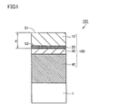
- FIG. 1 is a schematic cross-sectional view showing an example of the configuration of a surface-coated boron nitride sintered body tool (hereinafter referred to as “coated cBN tool”) according to the first embodiment.
- the coated cBN tool 101 includes a base material 1 made of a cBN sintered body and a coating 100 formed thereon.
- the coating 100 includes an A layer 10 and a C layer 30.
- the coating 100 has an outermost surface S1, and the C layer 30 has an upper surface S2.
- the A layer 10 is Ti 1-xa Maxa C 1-ya N ya (where Ma is one or more of Cr, Nb and W, xa is 0 ⁇ xa ⁇ 0.7, and ya is 0 ⁇ ya) ⁇ 1) and has the effect of smoothening the wear of crater wear and flank wear (ie, crater wear resistance and flank wear resistance).
- the C layer 30 is Al 1- (xc + yc) Cr xc Mc yc N (where Mc is one or more of Ti, V and Si, xc is 0.2 ⁇ xc ⁇ 0.8, yc Is 0 ⁇ yc ⁇ 0.6, and xc + yc is 0.2 ⁇ xc + yc ⁇ 0.8), and has an action of suppressing the progress of boundary wear (ie, boundary wear resistance).
- the A layer 10 is formed on the outermost surface S1 of the coating 100.
- the A layer 10 may be formed on the outermost surface S1 side with respect to the upper surface S2 of the C layer 30, and the A layer 10 may not be formed on the outermost surface S1.
- another layer a coloring layer made of TiN or the like
- the A layer 10 in the present embodiment is formed between the outermost surface S1 of the coating or the outermost surface S1 and the upper surface S2 of the C layer 30.
- the distance d between the outermost surface S1 of the coating 100 and the upper surface S2 of the C layer 30 is not less than 0.1 ⁇ m and not more than 1.0 ⁇ m.
- the maximum length of boundary wear at the beginning of cutting is regulated to a certain value or less.
- the distance d is more preferably 0.3 ⁇ m or more and 0.7 ⁇ m or less.
- the distance d between the outermost surface S1 and the upper surface S2 of the C layer 30 is measured as follows. That is, the coated cBN tool is cut, and the cross section is measured by observing with a scanning electron microscope (SEM: Scanning Electron Microscope) or a transmission electron microscope (TEM: Transmission Electron Microscope).
- SEM Scanning Electron Microscope
- TEM Transmission Electron Microscope
- the cross-section observation sample can be produced using, for example, a focused ion beam device (FIB), a cross section polisher device (CP), or the like.
- FIB focused ion beam device
- CP cross section polisher device
- the measurement method is also applied to the measurement of the thickness of the coating itself or the thickness of each layer constituting the coating.
- composition of each layer constituting the coating is measured by an energy dispersive X-ray analyzer (EDX: Energy Dispersive X-ray spectroscopy) attached to the SEM or TEM.
- EDX Energy Dispersive X-ray analyzer
- the coating 100 includes the A layer 10 and the C layer 30. As long as the coating 100 includes the A layer 10 and the C layer 30, the coating 100 may include other layers. For example, as shown in FIG. 1, a B layer 20 (adhesion layer) described later may be included between the A layer 10 and the C layer 30, and will be described later between the C layer 30 and the substrate 1. The D layer 40 may be included.
- the coating 100 preferably has a thickness of 0.5 ⁇ m or more and 10 ⁇ m or less.
- the thickness of the coating is 0.5 ⁇ m or more, it is possible to prevent the tool life from being reduced due to the thin coating. Moreover, the chipping resistance in the initial stage of cutting can be improved because the thickness of the film is 10 ⁇ m or less.
- the thickness of the coating is more preferably 1.0 ⁇ m or more and 5.0 ⁇ m or less.
- the A layer 10 is Ti 1-xa Maxa C 1-ya N ya (where Ma is one or more of Cr, Nb and W, xa is 0 ⁇ xa ⁇ 0.7, and ya is 0 ⁇ ya ⁇ 1).
- the A layer has crater wear resistance and flank wear resistance, suppresses the occurrence of waviness due to the progress of crater wear and flank wear, and keeps the finished surface roughness of the work material favorable.
- xa is preferably 0 ⁇ xa ⁇ 0.5, more preferably 0 ⁇ xa ⁇ 0.3, and further preferably 0 ⁇ xa ⁇ 0.2. This is because the wear resistance tends to be improved when xa occupies this range.
- ya is preferably 0.1 ⁇ ya ⁇ 0.9, more preferably 0.2 ⁇ ya ⁇ 0.8, and further preferably 0.3 ⁇ ya ⁇ 0.9. 0.7.
- the thickness of the A layer 10 is preferably 0.1 ⁇ m or more and 0.7 ⁇ m or less, more preferably 0.2 ⁇ m or more and 0.6 ⁇ m or less, and further preferably 0.3 ⁇ m or more and 0.5 ⁇ m or less. This is because the flank wear resistance tends to be improved when the thickness of the A layer 10 occupies this range.
- the A layer 10 (Ti 1-xa Maxa C 1-ya N ya ) includes a region where the value of ya changes in an inclined or stepped manner in the thickness direction of the A layer (for example, the vertical direction in FIG. 1 and the like) It is preferable. For example, when ya is large on the base material 1 side of the A layer 10, the chipping resistance and peeling resistance tend to be improved. For example, when the value of ya is small on the upper surface side of the A layer, peeling, cracking, chipping, etc. of the A layer 10 during wear can be prevented.
- the value of ya changes in an inclined manner in the thickness direction of the A layer means that the value of ya continuously decreases or increases from the lower surface of the A layer 10 toward the upper surface of the A layer 10. Show.
- AIP arc ion plating
- the value of ya changes stepwise in the thickness direction of the A layer indicates that the value of ya decreases or increases discontinuously from the lower surface of the A layer 10 toward the upper surface of the A layer 10. .
- Such a configuration can be obtained, for example, by stacking two or more layers having different values of ya.
- the C layer 30 is made of Al 1- (xc + yc) Cr xc Mc yc N (where Mc is one or more of Ti, V, and Si, xc is 0.2 ⁇ xc ⁇ 0.8, yc Is 0 ⁇ yc ⁇ 0.6, and xc + yc is 0.2 ⁇ xc + yc ⁇ 0.8). Accordingly, the C layer has boundary wear resistance.
- yc is preferably 0 ⁇ yc ⁇ 0.4, more preferably 0 ⁇ yc ⁇ 0.3, and further preferably 0 ⁇ yc ⁇ 0.2.
- Xc + yc is preferably 0.2 ⁇ xc + yc ⁇ 0.6, and more preferably 0.2 ⁇ xc + yc ⁇ 0.4.
- the C layer preferably has a thickness of 0.1 ⁇ m or more and 1.0 ⁇ m or less. Thereby, the development of boundary wear can be more reliably prevented.
- the thickness of the C layer is more preferably 0.1 ⁇ m or more and 0.7 ⁇ m or less, and further preferably 0.1 ⁇ m or more and 0.5 ⁇ m or less.
- the film 100 shown in FIG. 1 has a B layer 20 as an adhesion layer between the A layer 10 and the C layer 30. Thereby, peeling between the A layer 10 and the C layer 30 is prevented.
- the B layer 20 preferably contains one or more compounds selected from the group consisting of Al, Cr and Ti and one or more compounds composed of N. Such a compound has high affinity with both of the A layer 10 and the C layer 30, and can adhere strongly to both.
- the thickness of the B layer 20 is preferably 0.005 ⁇ m or more and 0.7 ⁇ m or less, more preferably 0.1 ⁇ m or more and 0.6 ⁇ m or less, and further preferably 0.1 ⁇ m or more and 0.4 ⁇ m or less.
- the B layer 20 for example, one or more B1 layers (not shown) made of TiN and B2 layers (not shown) made of AlCrN are alternately stacked. It can be a multilayer structure. Thereby, the B layer 20 can be a layer having high affinity with both the A layer 10 and the C layer 20 as a whole. Thereby, the B layer 20 can also contribute to improvement of crater wear resistance and flank wear resistance.
- the thicknesses of the B1 layer and the B2 layer can be 0.5 nm or more and less than 30 nm, respectively.
- the number of stacked layers is, for example, 4 to 50 layers, preferably 8 to 40 layers, and more preferably 10 layers. There are 20 layers or less.
- the B1 layer and the B2 layer are alternately arranged so that the layer in contact with the A layer 10 is the B1 layer (TiN layer) and the layer in contact with the C layer is the B2 layer (AlCrN layer). It is preferable to laminate them.
- the B layer 20 may have a single layer structure.
- the B layer 20 preferably contains a compound composed of AlTiCrN. Since AlTiCrN is a compound having a composition that is almost in the middle of the compounds constituting the A layer 10 and the C layer 30, even a single layer can exhibit sufficient adhesion.
- the coating 100 may include a D layer 40 between the C layer 30 and the substrate 1.
- the D layer 40 is, for example, MdLd zd (Md is one or more of Group 4 element, Group 5 element and Group 6 element of the periodic table, Al and Si, and Ld is B (boron), C, N and 1 or more of O (oxygen), and zd is 0 ⁇ zd ⁇ 1.0).
- MdLd zd MdLd zd
- Ld B (boron)
- zd is 0 ⁇ zd ⁇ 1.0
- the thickness of the D layer 40 is, for example, not less than 0.5 ⁇ m and not more than 3.0 ⁇ m, and preferably not less than 1.0 ⁇ m and not more than 2.0 ⁇ m.
- the cBN sintered body of the present embodiment constitutes the base material 1 of the tool among the cutting edge portions of the coated cBN tool 101.
- the cBN sintered body only needs to be provided on the cutting edge portion of the coated cBN tool 101. That is, the base material of the coated cBN tool may include a cutting edge portion made of a cBN sintered body and a base body made of a material different from the cBN sintered body (for example, a cemented carbide). In this case, it is preferable that the cutting edge part which consists of a cBN sintered compact is adhere
- the brazing material may be appropriately selected in consideration of bonding strength and melting point.
- the cBN sintered body may constitute the entire base material of the coated cBN tool 101.
- the cBN sintered body preferably contains cBN particles in the range of 30% by volume to 80% by volume, and further contains a binder phase as the balance.
- the binder phase is at least one selected from the group consisting of nitrides, carbides, borides, oxides, and solid solutions of Group 4 elements, Group 5 elements and Group 6 elements of the periodic table. It is preferable that an aluminum compound and an unavoidable impurity are included.
- the binder phase binds the cBN particles to each other in the sintered body structure. By containing 30% by volume or more of cBN particles in the sintered body structure, it is possible to prevent a decrease in wear resistance of the cBN sintered body. Further, by containing 80% by volume or less of cBN particles, cBN particles having excellent strength and toughness in the sintered body structure can play a role of a skeletal structure, and ensure the fracture resistance of the cBN sintered body. Can do.
- the volume content of cBN particles is measured by the following method. That is, the cBN sintered body is mirror-polished, and the reflected electron image of the cBN sintered body structure in an arbitrary region is observed using a SEM at a magnification of 2000 times. At this time, the cBN particles are observed as a black region, and the binder phase is observed as a gray region or a white region. Then, in the observation visual field image, the cBN particle region and the binder phase region are binarized by image processing, and the occupied area of the cBN particle region is measured. Then, the volume content of the cBN particles can be calculated by substituting the occupied area into the following equation.
- the volume content of cBN particles is more preferably 50% by volume to 75% by volume.
- the coated cBN tool tends to have an excellent balance between wear resistance and fracture resistance.
- the binder phase is appropriately distributed when the volume content of the cBN particles is 75% by volume or less, the bonding strength between the cBN particles due to the binder phase tends to increase.
- the volume content of cBN particles is particularly preferably 50% by volume or more and 60% by volume or less.
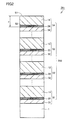
- FIG. 2 is a schematic cross-sectional view showing an example of the configuration of the coated cBN tool according to the second embodiment.
- the coated cBN tool 201 according to the second embodiment includes a base material 1 made of a cBN sintered body and a coating 200 formed thereon, and the coating 200 includes a plurality of coatings.
- a layer first A layer 11, second A layer 12, third A layer 13 and fourth A layer 14
- a plurality of C layers first C layer 31 and second C layer 32
- Third C layer 33 and fourth C layer 34 Third C layer 33 and fourth C layer 34.
- the coating 200 includes four stacked units having an A layer on the C layer.
- the thickness of the coating 200 is preferably 0.5 ⁇ m or more and 10 ⁇ m or less, more preferably 1.0 ⁇ m or more and 5.0 ⁇ m or less, as in the first embodiment.
- the configuration shown in FIG. 2 is merely an example, and in this embodiment, the number of stack units that the film has may be one (first embodiment) or may be two to three. Or five or more may be sufficient.
- the configuration of the first A layer 11, the second A layer 12, the third A layer 13, and the fourth A layer 14 is the same as the configuration of the A layer 10 described in the first embodiment. be able to.
- the first to fourth A layers may be different in thickness and composition.
- the third A layer 13 second A layer from the outermost surface S1 side
- the fourth A layer 14 A layer closest to the outermost surface S1
- the progress rate of the boundary wear in the third stack unit 53 is that in the fourth stack unit 54. This is because they may be different.
- the configurations of the first C layer 31, the second C layer 32, the third C layer 33, and the fourth C layer 34 are the same as the configuration of the C layer 30 described in the first embodiment.
- the thickness and composition of each C layer may be different.
- the fourth A layer 14 constitutes the outermost surface S1 of the coating. That is, the fourth A layer 14 is formed on the outermost surface S ⁇ b> 1 of the coating 200.
- the distance d between the outermost surface S1 of the coating 200 and the upper surface S2 of the fourth C layer 34 is not less than 0.1 ⁇ m and not more than 1.0 ⁇ m.
- the distance d between the outermost surface S1 of the coating and the upper surface S2 of the C layer is C closest to the outermost surface S1 among the plurality of C layers.
- the distance between the upper surface S2 of the layer and the outermost surface S1 shall be indicated.
- another layer may be formed on the fourth A layer 14.
- the coating 200 includes four stack units (first stack unit 51, second stack unit 52, third stack unit 53, and fourth stack unit 54) having the A layer on the C layer. Yes. Thereby, it is possible to maintain a good finished surface roughness over a long period of time and to have an excellent surface roughness life. That is, even if the fourth laminated unit 54 disappears due to wear, the third laminated unit 53 to the first laminated unit 51 have the same action, so that the development of boundary wear and the development of flank wear are again suppressed. be able to.
- B layers (first B layer 21, second B layer 22, third B layer 23, and fourth B layer 24) are formed between each A layer and each C layer. Has been. Thereby, the adhesiveness in each laminated unit increases and the surface roughness life is improved.
- An arbitrary layer may be included between the respective stacked units.
- the first stacked unit 51 and the second stacked unit 52 are formed close to each other, the first A layer 11 and the second stacked unit 52 It is preferable to provide a B layer (adhesion layer) between the two C layers 32. As a result, the adhesion between the stacked units increases, so that the surface roughness life can be further improved.
- the layer in contact with the substrate 1 is preferably a C layer (the first C layer 31 in FIG. 2). Since the C layer having the above-described composition is excellent in adhesion to the cBN sintered body, the layer 200 in contact with the substrate 1 can be prevented from falling off or peeling off from the entire coating 200.
- the coated cBN tool of the present embodiment described above can be manufactured as follows.
- the base material of this embodiment can be manufactured by joining a base material body and a base material made of a cBN sintered body.
- a material of the base body for example, a cemented carbide can be used.
- Such a base body can be produced by, for example, a conventionally known sintering method and molding method.
- the base material which consists of a cBN sintered compact can be manufactured by sintering the mixture which consists of a raw material powder of cBN particle
- a base material can be manufactured by joining the base material which consists of a cBN sintered compact to the suitable site
- the entire base material can be formed of a cBN sintered body.
- a coated cBN tool can be produced by forming a coating on the substrate obtained as described above.
- the coating is preferably formed by an AIP method (ion plating method in which a solid material is evaporated using vacuum arc discharge) or a sputtering method.
- AIP method ion plating method in which a solid material is evaporated using vacuum arc discharge
- a sputtering method ion plating method in which a solid material is evaporated using vacuum arc discharge
- a film can be formed by using a metal evaporation source containing a metal species that constitutes the film and a reactive gas such as CH 4 , N 2, or O 2 .
- a condition for forming the film a conventionally known condition can be employed.
- the film is formed by using a metal evaporation source including a metal species constituting the film, a reactive gas such as CH 4 , N 2, or O 2 and a sputtering gas such as Ar, Kr, or Xe. Can be formed.
- a metal evaporation source including a metal species constituting the film, a reactive gas such as CH 4 , N 2, or O 2 and a sputtering gas such as Ar, Kr, or Xe.
- a conventionally known condition can be adopted as a condition for forming the film.
- the present embodiment will be described in more detail using examples, but the present embodiment is not limited to these.
- the first A layer 11 and the second A layer 12 may be collectively referred to simply as the A layer.
- CBN sintered bodies A to H having the compositions shown in Table 1 were produced as follows.
- the compounds shown in the column of “X-ray detection compound” in Table 1 are compounds detected when the cross section or surface of the cBN sintered body is qualitatively analyzed by an X-ray diffraction (XRD) apparatus.
- the mixture was heat treated in a vacuum at 1000 ° C. for 30 minutes.
- the compound obtained by the heat treatment was uniformly pulverized by a ball mill pulverizing method using a cemented carbide ball media having a diameter of 6 mm. This obtained the raw material powder of the binder phase.
- a boron nitride ball having a diameter of 3 mm is prepared by blending cBN particles having an average particle diameter of 1.5 ⁇ m and a raw material powder of a binder phase so that the content of cBN particles in the cBN sintered body is 30% by volume.
- the mixture was uniformly mixed by a ball mill mixing method to obtain a powdery mixture.
- the mixture was laminated on a cemented carbide support substrate and then filled into Mo capsules. Subsequently, it was sintered for 30 minutes at a pressure of 5.5 GPa and a temperature of 1300 ° C. using an ultrahigh pressure apparatus. As a result, a cBN sintered body A was obtained.
- cBN sintered bodies B to F Manufacture of cBN sintered bodies B to F
- Table 1 cBN sintered bodies B to F were obtained in the same manner as the cBN sintered body A, except that the volume content and average particle size of the cBN particles were changed.
- the mixture was heat treated in a vacuum at 1000 ° C. for 30 minutes.
- the compound obtained by the heat treatment was uniformly pulverized by a ball mill pulverizing method using a cemented carbide ball media having a diameter of 6 mm. This obtained the raw material powder of the binder phase.
- cBN sintered compact G was obtained like cBN sintered compact A except changing the volume content and average particle diameter of cBN particles as shown in Table 1. .
- the mixture was heat treated in a vacuum at 1000 ° C. for 30 minutes.
- the compound obtained by the heat treatment was uniformly pulverized by a ball mill pulverizing method using a cemented carbide ball media having a diameter of 6 mm. This obtained the raw material powder of the binder phase.
- a cBN sintered body H was obtained in the same manner as the cBN sintered body A, except that the raw material powder of the binder phase was used and the volume content and average particle size of the cBN particles were changed as shown in Table 1.
- a base body made of a cemented carbide material (equivalent to K10) having an ISO standard DNGA150408 shape was prepared.
- the above-mentioned cBN sintered body A shape: apex angle is 55 ° and both sides sandwiching the apex angle are 2 mm each on the bottom edge of the base material body (corner portion), and the thickness is 2 mm. Of a triangular prism).
- a brazing material made of Ti—Zr—Cu was used for the joining.
- the outer peripheral surface, the upper surface, and the lower surface of the joined body were ground to form a negative land shape (a negative land width of 150 ⁇ m and a negative land angle of 25 °) at the cutting edge.
- a negative land shape a negative land width of 150 ⁇ m and a negative land angle of 25 °
- a vacuum pump is connected to the film forming apparatus, and the apparatus has a vacuum chamber that can be evacuated.
- a rotary table is installed in the vacuum chamber, and the rotary table is configured so that a substrate can be set via a jig.
- the base material set in the vacuum chamber can be heated by a heater installed in the vacuum chamber.
- a gas pipe for introducing a gas for etching and film formation is connected to the vacuum chamber via a mass flow controller (MFC) for flow rate control.
- MFC mass flow controller
- a tungsten filament for generating etching Ar ions, and an arc evaporation source or sputtering source for film formation connected to a necessary power source are arranged.
- An evaporation source material (target) necessary for film formation is set in the arc evaporation source or the sputtering source.
- the base material obtained as described above was set in a vacuum chamber of a film forming apparatus, and the inside of the chamber was evacuated. Thereafter, the substrate was heated to 500 ° C. while rotating the rotary table at 3 rpm. Next, Ar gas was introduced into the vacuum chamber, the tungsten filament was discharged to generate Ar ions, a bias voltage was applied to the substrate, and the substrate was etched with Ar ions.
- the etching conditions at this time are as follows: Ar gas pressure: 1 Pa Substrate bias voltage: -500V.
- a B layer was formed on the A layer in the film forming apparatus. Specifically, a total number of layers is obtained by alternately forming five layers of B1 layers (not shown) made of TiN and B2 layers (not shown) made of AlCrN under the conditions shown below. And 10 layers were formed, and a B layer having a total thickness of 0.1 ⁇ m was formed. In the formation of the B layer, the deposition time was adjusted so that the thickness of the B1 layer was 10 nm and the thickness of the B2 layer was 10 nm. Sample No. 1, the uppermost layer (C layer side) of the B layer is the B2 layer, and the lowermost layer (A layer side) is the B1 layer.
- the B layer having the same configuration is also referred to as “B 0 layer”.
- the B layer has a multilayer structure including a B1 layer (TiN layer) and a B2 layer (AlCrN layer), the A layer side is laminated as the B1 layer and the C layer side is laminated as the B2 layer.
- the B1 layer was formed under the following conditions: Target: Ti Introduced gas: N 2 Deposition pressure: 3Pa Arc discharge current: 150 A Substrate bias voltage: -40V.
- the B2 layer was formed under the following conditions Target: Al (50 atomic%), Cr (50 atomic%) Introduced gas: N 2 Deposition pressure: 3Pa Arc discharge current: 150 A Substrate bias voltage: -50V.
- a C layer was formed on the B layer. Specifically, the C layer was formed by adjusting the deposition time so that the thickness was 0.2 ⁇ m under the following conditions: Target: Al (70 atomic%), Cr (30 atomic%) Introduced gas: N 2 Deposition pressure: 4Pa Arc discharge current: 150 A Substrate bias voltage: -35V Table rotation speed: 3 rpm.
- sample no. A coated cBN tool according to 1 was obtained.
- Sample No. The outermost surface of one coating is composed of a C layer.
- Sample No. 2 to No. In No. 5 the distance d was 0.1 ⁇ m or more and 1.0 ⁇ m or less, and both the wear amount and the finished surface roughness were compatible.
- a cubic boron nitride sintered body and a film formed thereon are provided, and the film includes an A layer and a C layer, and the A layer is Ti 1-xa Maxa C 1-ya N ya (however, Ma Is one or more of Cr, Nb and W, xa is 0 ⁇ xa ⁇ 0.7, and ya is 0 ⁇ ya ⁇ 1, and the C layer is Al 1 ⁇ (xc + yc) Cr xc Mc yc N (where Mc is one or more of Ti, V and Si, xc is 0.2 ⁇ xc ⁇ 0.8, yc is 0 ⁇ yc ⁇ 0.6, and xc + yc) Is 0.2 ⁇ xc + yc ⁇ 0.8), and the A layer is formed between the outermost surface of the coating or between the outermost surface of the coating and the C layer, and between the outermost surface of the coating and the upper surface of the C layer.
- the distance is
- Example 2 Examination of configuration of layer A> (Production of sample No. 7) Sample no. A coated cBN tool according to 7 was produced.
- a base material 1 was obtained in the same manner as in Example 1 except that the cBN sintered body C was used instead of the cBN sintered body A.
- the C layer 30 was formed on the D layer 40. Specifically, the C layer 30 was formed by adjusting the deposition time so that the thickness was 0.2 ⁇ m under the following conditions: Target: Al (70 atomic%), Cr (30 atomic%) Introduced gas: N 2 Deposition pressure: 4Pa Arc discharge current: 150 A Substrate bias voltage: -35V Table rotation speed: 3 rpm.
- the B layer 20 having a multilayer structure composed of the B1 layer and the B2 layer and having a thickness of 0.1 ⁇ m was formed in the same manner as the B layer in Example 1.
- a coated cBN tool including the coating 100 including the A layer 10 and the C layer 30 on the cBN sintered body was obtained.
- Sample No. 7 the A layer 10 is formed on the outermost surface S ⁇ b> 1 of the coating 100, and the distance d between the outermost surface S ⁇ b> 1 and the upper surface S ⁇ b> 2 of the C layer 30 is 0.6 ⁇ m.
- Sample No. The configuration of 7 is shown in Table 4.
- Sample No. 11 after forming the D layer 40, the C layer 30, and the B layer 20 on the substrate 1 in the same manner as described above, ya in the formula Ti 1 -xa Max C 1 -ya Nya is the thickness direction of the coating.
- the A layer 10 including a region that changes in an inclined shape or a step shape is formed.
- Table 4 the composition of the A layer 10 is described as “TiCN * 01 ” for convenience. Specifically, the A layer was formed as follows.
- ya is preferably 0 ⁇ ya ⁇ 0.9, and more preferably 0 ⁇ ya ⁇ 0.5.
- Mc in the A layer can be Cr, Nb and W. Furthermore, sample no. 11-No. From the result of 16, it can be said that the A layer preferably includes a region where ya changes in an inclined shape or a step shape in the thickness direction of the A layer.
- Example 3 Examination of composition of C layer> (Production of sample Nos. 18 to 22)
- the base material 1 was obtained in the same manner as in Example 1 except that the cBN sintered body D was used instead of the cBN sintered body A, and the D layer 40, the C layer 30, the B layer 20, and the composition and composition shown in Table 6 were obtained.
- Sample No. 2 was prepared in the same manner as in Example 2 except that the coating 100 was formed by laminating the A layer 10 in this order. Coated cBN tools according to 18-22 were obtained.
- Example 4 Examination of thickness of C layer> (Production of sample No. 23) (Formation of substrate) A substrate 1 was obtained in the same manner as in Example 1 except that the cBN sintered body E was used instead of the cBN sintered body A.
- a coating film 200 including two laminated units having an A layer on a C layer was formed on a substrate 1.
- An Al 0.8 Cr 0.2 N layer having a thickness of 0.05 ⁇ m was formed as the first C layer 31 on the substrate 1.
- an Al 0.5 Ti 0.3 Cr 0.2 N layer having a thickness of 0.1 ⁇ m was formed as a first B layer 21 thereon.
- the first A layer 11 has a thickness of 0.3 ⁇ m, and ya in the formula Ti 1-xa Maxa C 1-ya Nya changes in an inclined or stepped manner in the thickness direction of the coating.
- a TiCN * 01 layer including the region was formed. Thereby, the first stack unit 51 was formed.
- a second layer having the same configuration as the first stack unit 51 is formed thereon.
- a stacked unit 52 was formed. That is, a film including two laminated units having the A layer was formed on the C layer.
- sample No. A coated cBN tool according to 23 was obtained.
- Sample No. Table 7 shows the configuration of 23.
- the description of the B layer (Al 0.5 Ti 0.3 Cr 0.2 N layer) between the first stack unit and the second stack unit is omitted.
- the description in the table is omitted for the B layer formed between the respective stacked units.
- “number of stacked units” indicates the number of stacked units having the A layer on the C layer (hereinafter the same).
- sample Nos. 24-27 As shown in Table 7, sample No. 1 was changed except that the thickness of the C layer was changed in the first stack unit 51 and the second stack unit 52. Similar to sample No. 23, sample no. Coated cBN tools according to 24-27 were obtained.
- Sample No. Sample No. 23 has the same coating composition except for the thickness of the C layer. 24-No. The result was slightly inferior to the machining accuracy compared to 26. This is probably because the thickness of the C layer is slightly thinner, so that the development of boundary wear is larger than the others. Sample No. No. 27 had a slightly larger wear amount than the others. The reason for this is considered that the progress of the flank wear is accelerated because the thickness of the C layer is slightly thick. Therefore, from these results, it can be said that the C layer preferably has a thickness of 0.1 ⁇ m or more and 1.0 ⁇ m or less, and more preferably has a thickness of 0.11 ⁇ m or more and 0.9 ⁇ m or less.
- Example 5 Examination of configuration of layer B> (Production of sample Nos. 29 to 33) A substrate 1 was obtained in the same manner as in Example 1 except that cBN sintered body H was used instead of cBN sintered body A, and D layer 40, C layer 30, B layer 20 having the composition and configuration shown in Table 8 and Sample No. 2 was prepared in the same manner as in Example 2 except that the coating 100 was formed by laminating the A layer 10 in this order. 29-No. A coated cBN tool according to No. 33 was obtained. As shown in Table 8, Sample No. 29-No. In 33, in the B layer 20, the thickness of the B layer, the thickness of the B1 layer and the B2 layer, and the number of layers are different.
- Sample No. 28 the adhesion between the A layer 10 and the C layer 30 was low, and peeling occurred between the A layer 10 and the C layer 30.
- Sample No. No. 33 also resulted in a large amount of flank wear. The reason is considered to be that the thickness of the B layer 20 is thick.
- the coating includes a B layer between the A layer and the C layer, and the B layer includes a B1 layer composed of TiN and a B2 layer composed of AlCrN alternately. It can be said that the thickness of the B1 layer and the B2 layer is preferably 0.5 nm or more and less than 30 nm, respectively, including a multilayer structure in which at least one layer is laminated.
- Example 6 Examination of lamination unit (1)> (Production of sample No. 34) A base material 1 is obtained in the same manner as in Example 1 except that the cBN sintered body H is used instead of the cBN sintered body A, and the first C layer 31 having the composition and configuration shown in Table 9 is formed on the base material 1. , The first B layer 21 and the first A layer 11 are laminated in this order to form the coating film 200. A coated cBN tool according to No. 34 was obtained. Sample No. In 34, the number of laminated units having the A layer on the C layer is one.
- sample No. 36 As shown in Tables 9 to 11, by forming the first laminated unit 51, the second laminated unit 52, and the third laminated unit 53 in this order on the substrate 1, sample No. A coated cBN tool according to 36 was obtained. A B 0 layer (thickness: 0.1 ⁇ m) was formed between the stacked units, and the A layer and the C layer were adhered to each other.
- the coating preferably includes a plurality of A layers and a plurality of C layers, and preferably includes two or more stacking units having the A layer on the C layer. It can be said that it is more preferable to include the above.
- Example 7 Examination of lamination unit (2)> (Production of sample No. 37 to No. 40) A base material 1 is obtained in the same manner as in Example 1 except that the cBN sintered body C is used instead of the cBN sintered body A, and the respective lamination units shown in Tables 12 to 15 are laminated on the base material 1 in this order. As a result, sample no. 37-No. A coated cBN tool according to 40 was obtained. A B 0 layer (thickness: 0.1 ⁇ m) was formed as an adhesion layer between the stacked units. In Table 15, sample no. The number of stacked units of 37 is one. This is the sample No. Since 37 does not have C layer in the 1st lamination unit (Table 12), it has shown that it is one as a lamination unit which has A layer on C layer.
- the A layer included in each stack unit is Ti 1-xa Maxa C 1-ya Nya (where Ma is one or more of Cr, Nb and W, xa is 0 ⁇ xa ⁇ 0.7, and ya is 0 ⁇ ya ⁇ 1)
- C layer is Al 1- (xc + yc) Cr xc Mc yc N (where Mc is one or more of Ti, V and Si, xc is 0.2 ⁇ xc ⁇ 0.8, yc is It was confirmed that excellent machining accuracy and surface roughness life can be realized as long as the structure is 0 ⁇ yc ⁇ 0.6 and xc + yc is 0.2 ⁇ xc + yc ⁇ 0.8.
- Example 8 Examination of cBN sintered body> (Production of sample Nos. 41 to 46) As shown in Tables 16 to 18, a base material 1 was obtained in the same manner as in Example 1 except that cBN sintered bodies B to G were used instead of the cBN sintered body A. Sample No. 18 was formed by forming a coating film 200 in which the respective lamination units shown in FIG. 41-No. A coated cBN tool according to No. 46 was obtained. A B 0 layer (thickness: 0.1 ⁇ m) was formed as an adhesion layer between the stacked units.
- Example 9 Examination of layer B in the lamination unit> As shown in Tables 19 to 21, in each of the stacked units, the above-described sample No. 1 was used except that the B layer was not formed between the A layer and the C layer, and the B 0 layer was not formed between the stacked units. Similar to Sample No. 36, Sample No. A coated cBN tool according to 47 was obtained.
- a cBN sintered body and a coating formed thereon are provided, the coating includes an A layer and a C layer, and the A layer is Ti 1-xa Maxa C 1-ya N ya (however, , Ma is one or more of Cr, Nb, and W, xa is 0 ⁇ xa ⁇ 0.7, and ya is 0 ⁇ ya ⁇ 1, and the C layer is Al 1 ⁇ (xc + yc) Cr xc Mc yc N (where Mc is one or more of Ti, V and Si, xc is 0.2 ⁇ xc ⁇ 0.8, yc is 0 ⁇ yc ⁇ 0.6, And xc + yc is 0.2 ⁇ xc + yc ⁇ 0.8), and the A layer is formed on the outermost surface of the coating or between the outermost surface of the coating and the C layer, and the outermost surface of the coating and the upper surface of the C layer. It was confirmed that the coated cBN
Landscapes
- Chemical & Material Sciences (AREA)
- Engineering & Computer Science (AREA)
- Ceramic Engineering (AREA)
- Materials Engineering (AREA)
- Organic Chemistry (AREA)
- Structural Engineering (AREA)
- Mechanical Engineering (AREA)
- Chemical Kinetics & Catalysis (AREA)
- Metallurgy (AREA)
- Manufacturing & Machinery (AREA)
- Crystallography & Structural Chemistry (AREA)
- Cutting Tools, Boring Holders, And Turrets (AREA)
- Inorganic Chemistry (AREA)
- Physical Vapour Deposition (AREA)
Abstract
Description
まず、本発明の一実施形態(以下「本実施形態」とも記す)の概要を以下の(1)~(11)に列記して説明する。
以下、本実施形態に係る表面被覆窒化硼素焼結体工具についてより詳細に説明するが、本実施形態はこれらに限定されるものではない。
<表面被覆窒化硼素焼結体工具>
図1は第1の実施形態に係る表面被覆窒化硼素焼結体工具(以下「被覆cBN工具」と記す)の構成の一例を示す模式的な断面図である。図1に示すように被覆cBN工具101は、cBN焼結体から構成される基材1とその上に形成された被膜100とを備えている。被膜100はA層10とC層30とを含んでいる。被膜100は最表面S1を有し、C層30は上面S2を有する。
<被膜>
被膜100は、A層10とC層30とを含んでいる。被膜100はA層10とC層30とを含む限り、他の層を含んでいてもよい。たとえば、図1に示すようにA層10とC層30との間に後述するB層20(密着層)等を含んでいてもよいし、C層30と基材1との間に後述するD層40を含んでいてもよい。
A層10は、Ti1-xaMaxaC1-yaNya(ただし、MaはCr、NbおよびWの1種以上であり、xaは0≦xa≦0.7であり、yaは0≦ya≦1である)から構成される。これによりA層は耐クレータ摩耗性および耐逃げ面摩耗性を有し、クレータ摩耗および逃げ面摩耗の進行によるうねりの発生を抑え、被削材の仕上がり面粗さを良好に保つことができる。
A層10(Ti1-xaMaxaC1-yaNya)は、yaの値がA層の厚さ方向(たとえば図1等の縦方向)において傾斜状またはステップ状に変化する領域を含むことが好ましい。たとえば、A層10の基材1側においてyaが大きい場合、耐欠損性および耐剥離性が向上する傾向にある。またたとえば、A層の上面側においてyaの値が小さい場合は、摩耗時におけるA層10の剥離、割れ、チッピング等を防止することができる。
C層30は、Al1-(xc+yc)CrxcMcycN(ただし、McはTi、VおよびSiの1種以上であり、xcは0.2≦xc≦0.8であり、ycは0≦yc≦0.6であり、かつxc+ycは0.2≦xc+yc≦0.8である)から構成される。これによりC層は耐境界摩耗性を有する。
図1に示す被膜100はA層10とC層30との間に密着層としてB層20を有している。これによりA層10とC層30との間での剥離が防止される。B層20は、Al、CrおよびTiからなる群より選ばれる1種以上の元素と、Nとから構成される1種以上の化合物を含むことが好ましい。このような化合物はA層10およびC層30のいずれとも親和性が高く、双方に強く密着することができる。B層20の厚さは、好ましくは0.005μm以上0.7μm以下であり、より好ましくは0.1μm以上0.6μm以下であり、さらに好ましくは0.1μm以上0.4μm以下である。
図1に示すように被膜100は、C層30と基材1との間にD層40を含んでいてもよい。D層40は、たとえばMdLdzd(Mdは周期表の第4族元素、第5族元素および第6族元素、AlならびにSiの1種以上であり、LdはB(硼素)、C、NおよびO(酸素)の1種以上であり、zdは0≦zd≦1.0である)から構成することができる。このようなD層40を形成することにより被膜100と基材1との密着性を向上させるとともに、被膜100が薄いことに起因する工具寿命の低下を防止することができる。D層40の厚さは、たとえば0.5μm以上3.0μm以下であり、好ましくは1.0μm以上2.0μm以下である。
本実施形態のcBN焼結体は、被覆cBN工具101の切れ刃部分のうち当該工具の基材1を構成するものである。cBN焼結体は被覆cBN工具101の切れ刃部分に設けられていればよい。すなわち被覆cBN工具の基材はcBN焼結体からなる切れ刃部分と、cBN焼結体とは異なる材料(たとえば超硬合金)からなる基材本体とを含んでいてもよい。この場合、cBN焼結体からなる切れ刃部分はろう材等を介して基材本体に接着されていることが好ましい。ろう材は接合強度や融点を考慮し適宜選択すればよい。cBN焼結体は被覆cBN工具101の基材全体を構成していてもよい。
以下、本実施形態のうち第2の実施形態について説明する。図2は第2の実施形態に係る被覆cBN工具の構成の一例を示す模式的な断面図である。図2に示すように第2の実施形態に係る被覆cBN工具201は、cBN焼結体からなる基材1とその上に形成された被膜200とを備えている、そして被膜200は、複数のA層(第1のA層11、第2のA層12、第3のA層13および第4のA層14)と複数のC層(第1のC層31、第2のC層32、第3のC層33および第4のC層34)とを含んでいる。そして被膜200はC層の上にA層を有する積層単位を4つ含んでいる。
上記に説明した本実施形態の被覆cBN工具は、以下のようにして製造することができる。
本実施形態の基材は、基材本体とcBN焼結体からなる基材とを接合することにより製造することができる。基材本体の材料としては、たとえば超硬合金を用いることができる。このような基材本体は、たとえば従来公知の焼結法および成形法により製造することができる。またcBN焼結体からなる基材は、たとえばcBN粒子と結合相の原料粉末とからなる混合物を高温高圧下で焼結させることにより製造することができる。そして基材本体の適切な部位に、cBN焼結体からなる基材を従来公知のろう材で接合し、所定の形状に研削加工することにより基材を製造することができる。なお基材全体をcBN焼結体から構成することも当然可能である。
上記のようにして得られた基材に被膜を形成することにより被覆cBN工具を製造することができる。ここで被膜は、AIP法(真空アーク放電を利用して固体材料を蒸発させるイオンプレーティング法)またはスパッタリング法により形成されることが好ましい。AIP法では、被膜を構成することになる金属種を含む金属蒸発源とCH4、N2またはO2等の反応ガスとを用いて被膜を形成することができる。なお被膜を形成する条件としては、従来公知の条件を採用することができる。またスパッタリング法では、被膜を構成することになる金属種を含む金属蒸発源と、CH4、N2またはO2等の反応ガスと、Ar、Kr、Xe等のスパッタガスとを用いて被膜を形成することができる。なおこの場合も被膜を形成する条件としては従来公知の条件を採用することができる。
(cBN焼結体の製造)
以下のようにして表1に示す組成を有するcBN焼結体A~Hを製造した。表1中「X線検出化合物」の欄に示す化合物は、cBN焼結体の断面または表面をX線回折(XRD:X―Ray Diffraction)装置によって定性分析した際に検出された化合物である。

まず、原子比でTi:N=1:0.6となるように平均粒径1μmのTiN粉末と平均粒径が3μmのTi粉末とを混合することにより混合物を得た。該混合物を真空中1200℃で30分間熱処理してから粉砕した。これによりTiN0.6からなる金属間化合物粉末を得た。
表1に示すようにcBN粒子の体積含有率および平均粒径を変更する以外は、cBN焼結体Aと同様にしてcBN焼結体B~Fを得た。
まず、原子比でTi:C=1:0.6となるように平均粒径1μmのTiC粉末と平均粒径が3μmのTi粉末とを混合することにより混合物を得た。該混合物を真空中1200℃で30分間熱処理してから粉砕した。これによりTiC0.6からなる金属間化合物粉末を得た。
まず、原子比でTi:C:N=1:0.3:0.5となるように平均粒径1μmのTiCN粉末と平均粒径が3μmのTi粉末とを混合することにより混合物を得た。該混合物を真空中1200℃で30分間熱処理してから粉砕した。これによりTiC0.3N0.5からなる金属間化合物粉末を得た。
以下のようにして試料No.1に係る被覆cBN工具を製造した。
形状がISO規格のDNGA150408であり、超硬合金材料(K10相当)からなる基材本体を準備した。該基材本体の刃先(コーナ部分)に上記のcBN焼結体A(形状:頂角が55°であり当該頂角を挟む両辺がそれぞれ2mmである二等辺三角形を底面とし、厚さが2mmの三角柱状のもの)を接合した。なお接合にはTi-Zr-Cuからなるろう材を用いた。次いで該接合体の外周面、上面および下面を研削し、刃先にネガランド形状(ネガランド幅が150μmであり、ネガランド角が25°)を形成した。このようにして切れ刃部分がcBN焼結体Aからなる基材を得た。
(成膜装置)
まずここで、以降の工程において被膜の形成に用いる成膜装置について説明する。当該成膜装置には真空ポンプが接続されており、装置内部に真空引き可能な真空チャンバーを有している。真空チャンバー内には、回転テーブルが設置されており、該回転テーブルは治具を介して基材がセットできるように構成されている。真空チャンバー内にセットされた基材は、真空チャンバー内に設置されているヒーターにより加熱することができる。また真空チャンバーにはエッチングおよび成膜用のガスを導入するためのガス配管が、流量制御用のマスフローコントローラ(MFC:Mass Flow Controller)を介して接続されている。さらに真空チャンバー内には、エッチング用のArイオンを発生させるためのタングステンフィラメント、必要な電源が接続された成膜用のアーク蒸発源もしくはスパッタ源が配置されている。そしてアーク蒸発源もしくはスパッタ源には、成膜に必要な蒸発源原料(ターゲット)がセットされている。
上記のようにして得られた基材を、成膜装置の真空チャンバー内にセットし、チャンバー内の真空引きを行なった。その後、回転テーブルを3rpmで回転させながら基材を500℃に加熱した。次いで、真空チャンバー内にArガスを導入し、タングステンフィラメントを放電させてArイオンを発生させ、基材にバイアス電圧を印加し、Arイオンにより基材のエッチングを行なった。なお、このときのエッチング条件は次のとおりである
Arガスの圧力 :1Pa
基板バイアス電圧:-500V。
次に上記の成膜装置内でA層を基材上に形成した。具体的には次に示す条件で厚さ1.7μmのA層を形成した。このとき導入ガス(N2およびCH4)の流量は、A層においてC:N=2:8となるように調整した
ターゲット :Ti
導入ガス :N2、CH4
成膜圧力 :2Pa
アーク放電電流 :180A
基板バイアス電圧:-350V
テーブル回転数 :3rpm。
A層に続いて、上記の成膜装置内でA層の上にB層を形成した。具体的には、以下に示す条件で、TiNからなるB1層(図示せず)とAlCrNからなるB2層(図示せず)とをそれぞれ交互に5層ずつ繰り返して形成することにより、合計層数が10層であり、合計厚さ0.1μmのB層を形成した。B層の形成においては、B1層の厚さを10nm、B2層の厚さを10nmとなるように蒸着時間を調整した。なお試料No.1において、B層の最上層(C層側)はB2層であり、最下層(A層側)はB1層である。以下これと同様の構成を有するB層を「B0層」とも記す。またB層がB1層(TiN層)とB2層(AlCrN層)とからなる多層構造を有する場合は、A層側をB1層、C層側をB2層として積層されるものとする。
B1層は次に示す条件で形成した
ターゲット :Ti
導入ガス :N2
成膜圧力 :3Pa
アーク放電電流 :150A
基板バイアス電圧:-40V。
B2層は次に示す条件で形成した
ターゲット :Al(50原子%)、Cr(50原子%)
導入ガス :N2
成膜圧力 :3Pa
アーク放電電流 :150A
基板バイアス電圧:-50V。
次にB層上にC層を形成した。具体的には次に示す条件で厚さ0.2μmとなるように蒸着時間を調整してC層を形成した
ターゲット :Al(70原子%)、Cr(30原子%)
導入ガス :N2
成膜圧力 :4Pa
アーク放電電流 :150A
基板バイアス電圧:-35V
テーブル回転数 :3rpm。
試料No.1と同様にして基材上にA層、B層、C層をこの順で積層した。
続いてC層上に、上記と同様にして厚さ0.1μmのB層を形成した。
さらにB層上に、厚さを0.1μmとすることを除いては上記と同様してA層を形成した。以上のようにして、試料No.2に係る被覆cBN工具を得た。試料No.2の構成を表2および表3に記す。試料No.2において被膜の最表面S1にはA層が形成されており、最表面S1とC層の上面S2との距離dは0.2μmである。
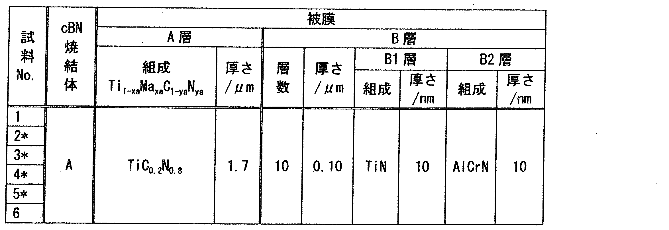
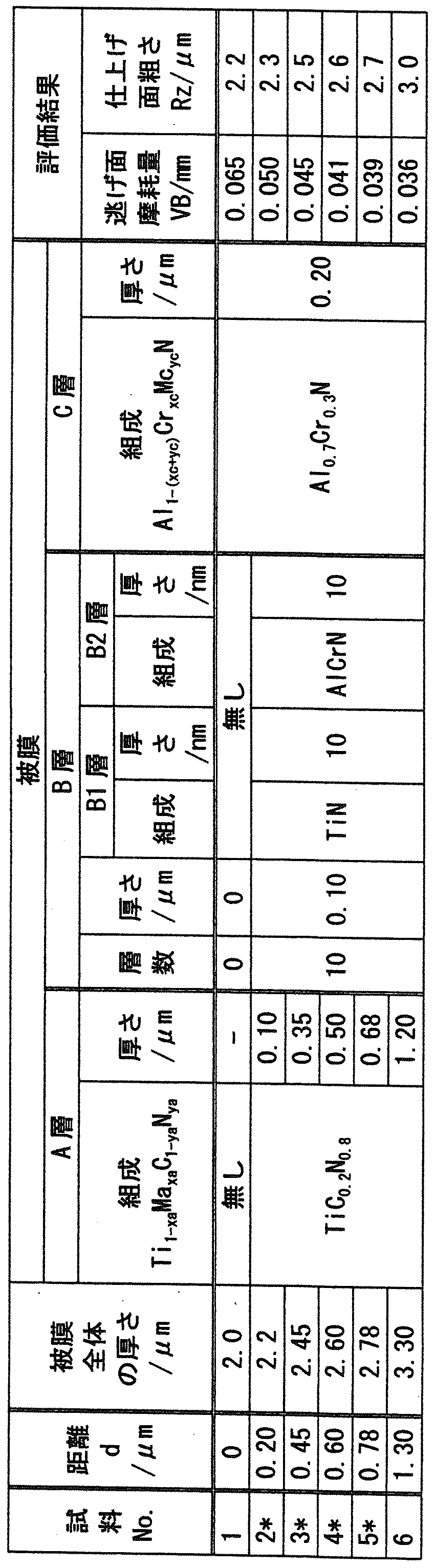
蒸着時間を調整して最表面S1に形成されたA層の厚さを表3に示すように変更する以外は、試料No.2と同様にして試料No.3~No.6に係る被覆cBN工具を得た。表2および表3中「No.」に「*」が付された試料が実施例に相当する(以下の実施例の説明についても同様とする。)。
以上のようにして得られた試料No.1~No.6に係る被覆cBN工具の切削性能と仕上げ面粗さを焼入鋼の連続切削により評価した。
各試料の工具を用いて、次に示す切削条件に従って切削距離3kmの切削加工を行なった。そして光学顕微鏡を使用して工具の逃げ面摩耗量VBを測定した。また「JIS B 0601」に準拠して、加工後の被削材の「十点平均粗さ(Rzjis)」を測定した。結果を表3に示す。表3中、逃げ面摩耗量VBが小さいほど耐摩耗性に優れる。またRzが小さいほど加工精度に優れることを示している。
被削材 :焼入鋼SCM415H(HRC60)、φ35mm×10mm
切削速度:150m/min
送り量 :f=0.1mm/rev
切込み :ap=0.1mm
切削油 :エマルジョン((株)日本フルードシステム社製の商品名「システムカット96」)を20倍に希釈したもの(wet状態)。
試料No.1は、Rzは小さいもののVBが大きい結果となった。この理由は、試料No.1はC層の上にA層を有しておらず、距離dが0.1μm未満であったためであると考えられる。また試料No.6は、VBは小さく良好であったがRzが大きい結果となった。これは距離dが1.0μmを超過したため境界摩耗の発達が大きくなったためであると考えられる。
(試料No.7の製造)
以下のようにして試料No.7に係る被覆cBN工具を製造した。
cBN焼結体Aの代わりにcBN焼結体Cを用いる以外は実施例1と同様にして基材1を得た。
以下のように図1を参照して、基材1上に被膜100を形成した。
実施例1と同様にして基材1のエッチングを行なった後、基材1上にD層40を形成した。具体的には次に示す条件で厚さ2.0μmとなるように蒸着時間を調整してD層40を形成した
ターゲット :Ti(30原子%)、Al(70原子%)
導入ガス :N2
成膜圧力 :4Pa
アーク放電電流 :150A
基板バイアス電圧:-35V
テーブル回転数 :3rpm。
次にD層40上にC層30を形成した。具体的には次に示す条件で厚さ0.2μmとなるように蒸着時間を調整してC層30を形成した
ターゲット :Al(70原子%)、Cr(30原子%)
導入ガス :N2
成膜圧力 :4Pa
アーク放電電流 :150A
基板バイアス電圧:-35V
テーブル回転数 :3rpm。
C層30を形成した後、実施例1におけるB層と同様にして、B1層とB2層とからなる多層構造を有し、厚さが0.1μmであるB層20を形成した。
B層20に続いてその上にA層10を形成した。具体的には次に示す条件で厚さ0.5μmのA層10を形成した。このとき導入ガス(N2およびCH4)の流量は、A層10においてC:N=1:1となるように調整した
ターゲット :Ti
導入ガス :N2、CH4
成膜圧力 :2Pa
アーク放電電流 :180A
基板バイアス電圧:-350V
テーブル回転数 :3rpm。
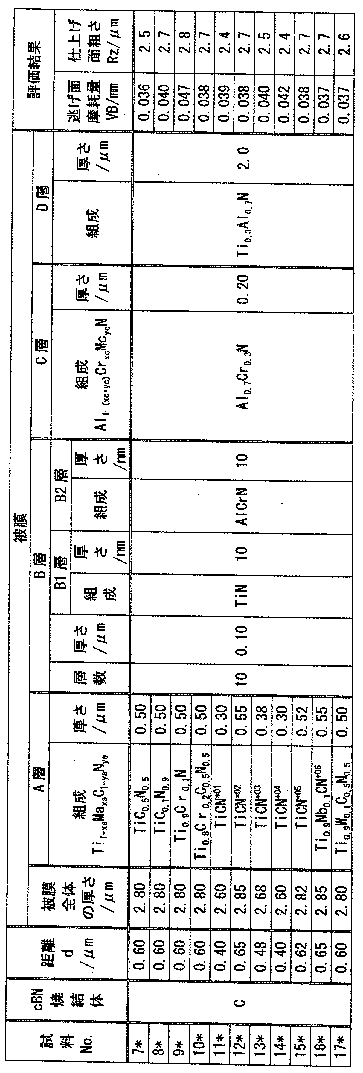
表4に示す組成のA層10が形成されるようにターゲット材料ならびに導入ガスの組成および流量を変更する以外は、試料No.7と同様にして試料No.8~No.10およびNo.17に係る被覆cBN工具を得た。
試料No.11では、上記と同様にして基材1上にD層40、C層30およびB層20を形成した後、式Ti1-xaMaxaC1-yaNyaにおけるyaが被膜の厚さ方向において傾斜状またはステップ状に変化する領域を含むA層10を形成した。表4中、当該A層10の組成を便宜上「TiCN*01」と記している。当該A層は具体的には次のようにして形成した。
まず、導入ガスとしてN2のみを使用し(すなわちya=1.0に固定し)、TiN層を0.05μm形成した。次に、導入ガス中のCH4の流量を徐々に増加させながら、ya(N組成)が傾斜状に減少する(1-ya(C組成)は傾斜状に増加する)TiCN層を0.2μm形成した。当該TiCN層の組成は最終的にTiC0.5N0.5であった(すなわちya=0.5)。その後、N2とCH4の流量比を固定してTiC0.5N0.5層を0.05μm形成した。このようにして、B層20の上に、Ti1-xaMaxaC1-yaNyaにおけるyaがA層10の厚さ方向に傾斜状に変化するA層10(TiCN*01)を形成した。これにより試料No.11に係る被覆cBN工具を得た。当該A層の構成を表5に示す。表5中、「Ti1-xaMaxaC1-yaNyaにおけるyaの値」の欄において、たとえば「1→0.5」はyaの値が1から0.5へと連続して減少することを示している。

表5に示す「TiCN*02」~「Ti0.9Nb0.1CN*06」の組成および構成を有するA層10を形成する以外は、試料No.11と同様にして試料No.12~No.16に係る被覆cBN工具を得た。
以上のようにして得られた試料No.7~17係る被覆cBN工具の切削性能と仕上げ面粗さを実施例1と同様にして焼入鋼の連続切削により評価した。結果を表4に示す。なお表4に示すように試料No.7~17ではA層10の構成がそれぞれ異なっている。
試料No.7とNo.8を比較するとyaの値が0.9、0.5と変化するにつれて耐摩耗性および加工精度が向上していることが分かる。したがって、yaは0≦ya≦0.9が好ましく、0≦ya≦0.5がより好ましいといえる。
(試料No.18~22の製造)
cBN焼結体Aの代わりにcBN焼結体Dを用いる以外は実施例1と同様にして基材1を得、表6に示す組成および構成のD層40、C層30、B層20およびA層10をこの順に積層して被膜100を形成する以外は、実施例2と同様にして試料No.18~22に係る被覆cBN工具を得た。
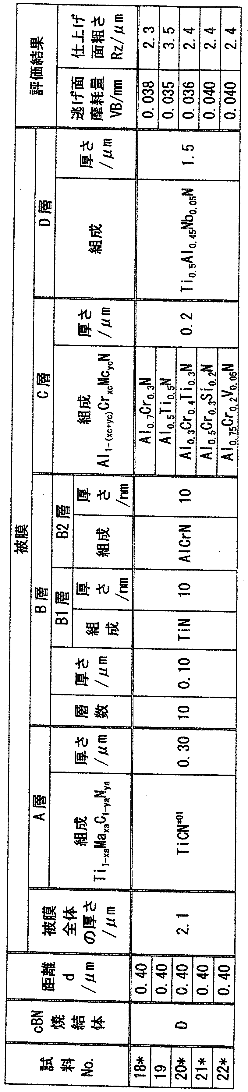
以上のようにして得られた試料No.18~No.22係る被覆cBN工具の切削性能と仕上げ面粗さを実施例1と同様にして焼入鋼の連続切削により評価した。結果を表6に示す。表6に示すように、試料No.18~No.22ではC層30の組成がそれぞれ異なっている。
No.18~No.22を比較するとC層30の組成を除いてはいずれも同様の構成を有するにも関わらず、試料No.19のみが加工精度において劣る結果となった。この理由は、試料No.19におけるC層はCrを含んでいないため(すなわちxcが0.2未満)、C層が境界摩耗の発達を十分に阻止できなかったからであると考えられる。
(試料No.23の製造)
(基材の形成)
cBN焼結体Aの代わりにcBN焼結体Eを用いる以外は実施例1と同様にして基材1を得た。
以下のように図2を参照して、基材1上にC層の上にA層を有する積層単位を2つ含む被膜200を形成した。
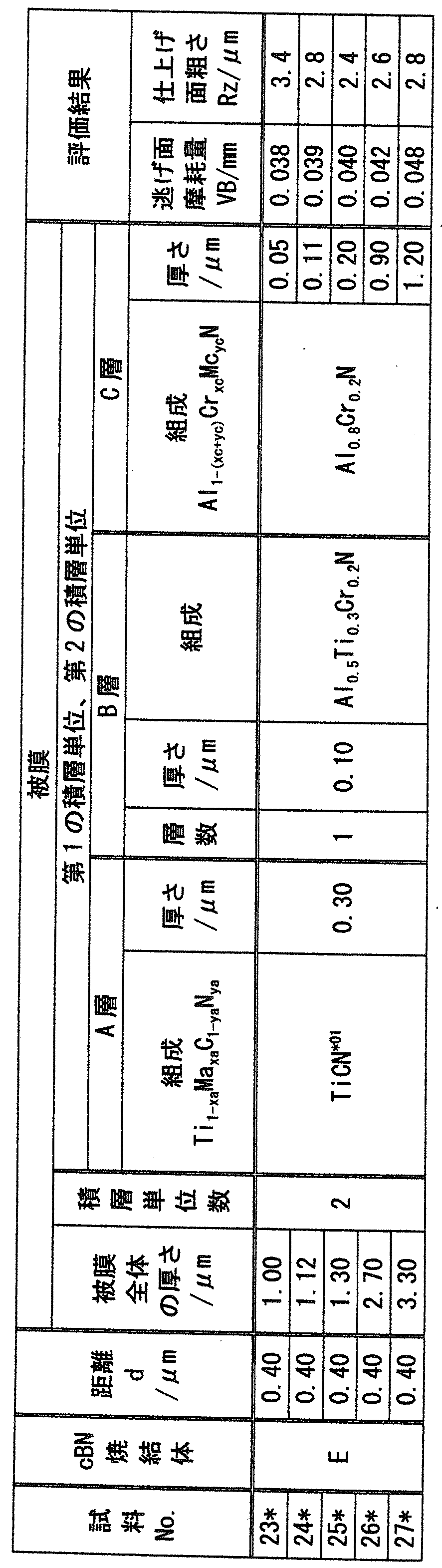
表7に示すように第1の積層単位51および第2の積層単位52においてC層の厚さを変更する以外は、試料No.23と同様して試料No.24~27に係る被覆cBN工具を得た。
以上のようにして得られた試料No.23~27に係る被覆cBN工具の切削性能と仕上げ面粗さを実施例1と同様にして焼入鋼の連続切削により評価した。結果を表7に示す。
試料No.23は、C層の厚さ以外は同様の被膜構成を有する試料No.24~No.26と比較して加工精度にやや劣る結果となった。この理由はC層の厚さがやや薄いため、境界摩耗の発達がその他に比して大きくなったと考えられる。また試料No.27はその他と比較して摩耗量がやや多い結果となった。この理由はC層の厚さがやや厚いため、逃げ面摩耗の進行が早まったためと考えられる。したがってこれらの結果から、C層は0.1μm以上1.0μm以下の厚さを有することが好ましく、0.11μm以上0.9μm以下の厚さを有することがより好ましいといえる。
(試料No.29~33の製造)
cBN焼結体Aの代わりにcBN焼結体Hを用いる以外は実施例1と同様にして基材1を得、表8に示す組成および構成のD層40、C層30、B層20およびA層10をこの順に積層して被膜100を形成する以外は、実施例2と同様にして試料No.29~No.33に係る被覆cBN工具を得た。表8に示すように、試料No.29~No.33ではB層20において、B層の厚さ、B1層およびB2層の厚さならびに層数がそれぞれ異なっている。

B層20を形成せず、C層30上に直接A層10を形成する以外は、試料No.29~No.33と同様にして、試料No.28に係る被覆cBN工具を得た。
以上のようにして得られた試料No.28~33に係る被覆cBN工具の切削性能と仕上げ面粗さを実施例1と同様にして焼入鋼の連続切削により評価した。結果を表8に示す。
(試料No.34の製造)
cBN焼結体Aの代わりにcBN焼結体Hを用いる以外は実施例1と同様にして基材1を得、基材1上に、表9に示す組成および構成の第1のC層31、第1のB層21および第1のA層11をこの順に積層して被膜200を形成することにより、試料No.34に係る被覆cBN工具を得た。試料No.34においてC層の上にA層を有する積層単位は1つである。
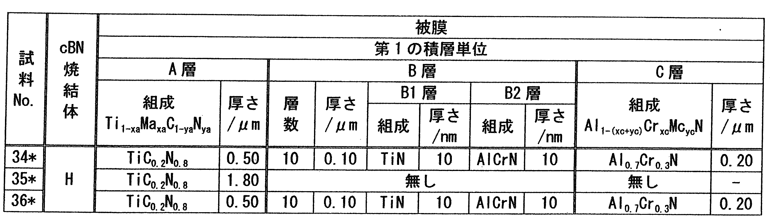
試料No.34と同様にして第1のA層11を形成した後、第1のA層11上に、密着層としてB0層(厚さ0.1μm)を形成し、さらにその上に表10に示す第2の積層単位52を形成することにより、試料No.35に係る被覆cBN工具を得た。試料No.35においてC層の上にA層を有する積層単位は1つである。
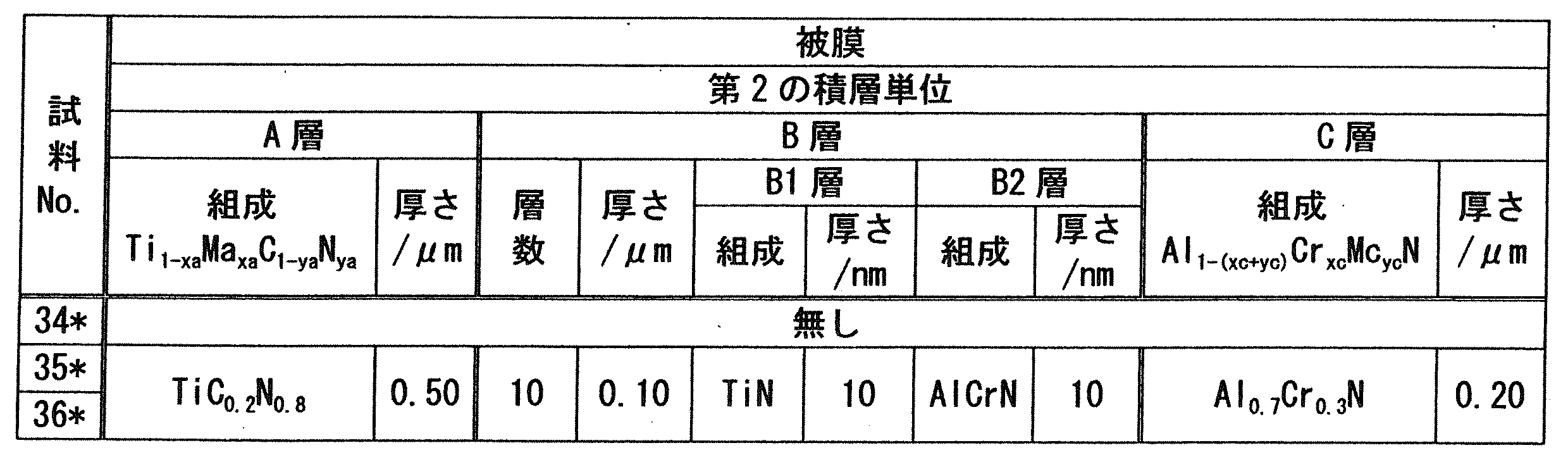
表9~表11に示すように、基材1上に第1の積層単位51、第2の積層単位52および第3の積層単位53をこの順に形成することにより、試料No.36に係る被覆cBN工具を得た。なお各積層単位の間にはB0層(厚さ0.1μm)を形成し、A層とC層とを密着させた。
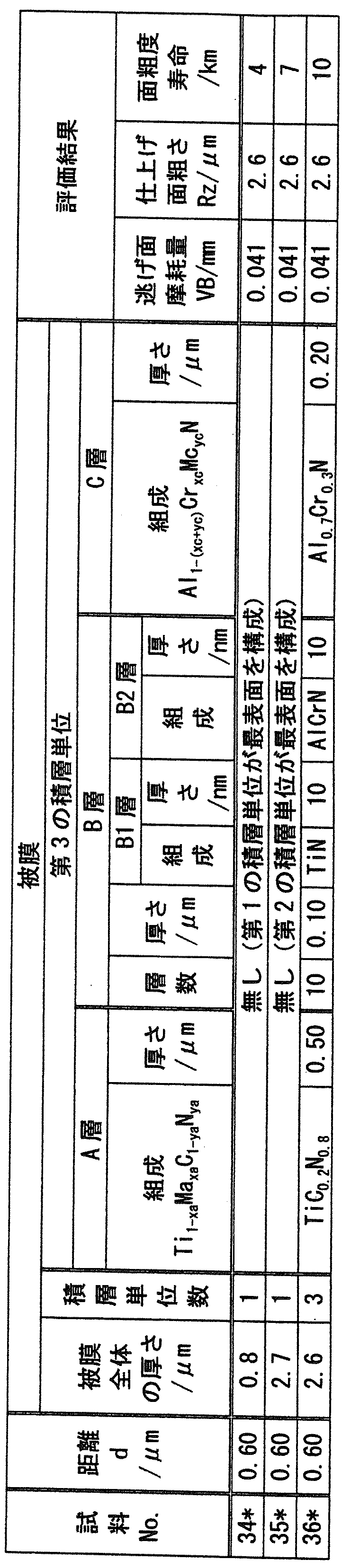
以上のようにして得られた試料No.34~36に係る被覆cBN工具の切削性能と仕上げ面粗さを実施例1と同様にして焼入鋼の連続切削により評価した。結果を表11に示す。
(面粗度寿命の測定)
寿命判定基準をRz=3.2μmとして、高精度加工における面粗度寿命を測定した。すなわち上記の切削条件で切削距離500mの加工を1セットとして繰り返し加工を行ない、1セットの加工が終了する度に表面粗さ計を使用して被削材の面粗さRzjisを測定し、Rzjisが3.2μmを超えた時点で試験終了とした。そして500m×セット回数から総切削距離(km)を算出した。さらに、Rzjisを縦軸、切削距離を横軸とする散布図を作成し、該散布図上において終了点と終了直前の点との2点を結ぶ直線上で、Rzが3.2μmに達する切削距離を面粗度寿命とした。その結果を表11に示す。
表9~表11に示すように、試料No.34~No.36において被膜の最表面から最も被膜の最表面側に位置するC層までの構成は同一である。そのため3km切削した時点での耐摩耗性および加工精度はほぼ同等であった。
(試料No.37~No.40の製造)
cBN焼結体Aの代わりにcBN焼結体Cを用いる以外は実施例1と同様にして基材1を得、基材1上に表12~表15に示す各積層単位をこの順で積層することにより、試料No.37~No.40に係る被覆cBN工具を得た。なお各積層単位の間には密着層としてB0層(厚さ0.1μm)を形成した。また表15では、試料No.37の積層単位数を1つとしている。これは、試料No.37は第1の積層単位においてC層を有していないため(表12)、C層の上にA層を有する積層単位としては1つであることを示している。
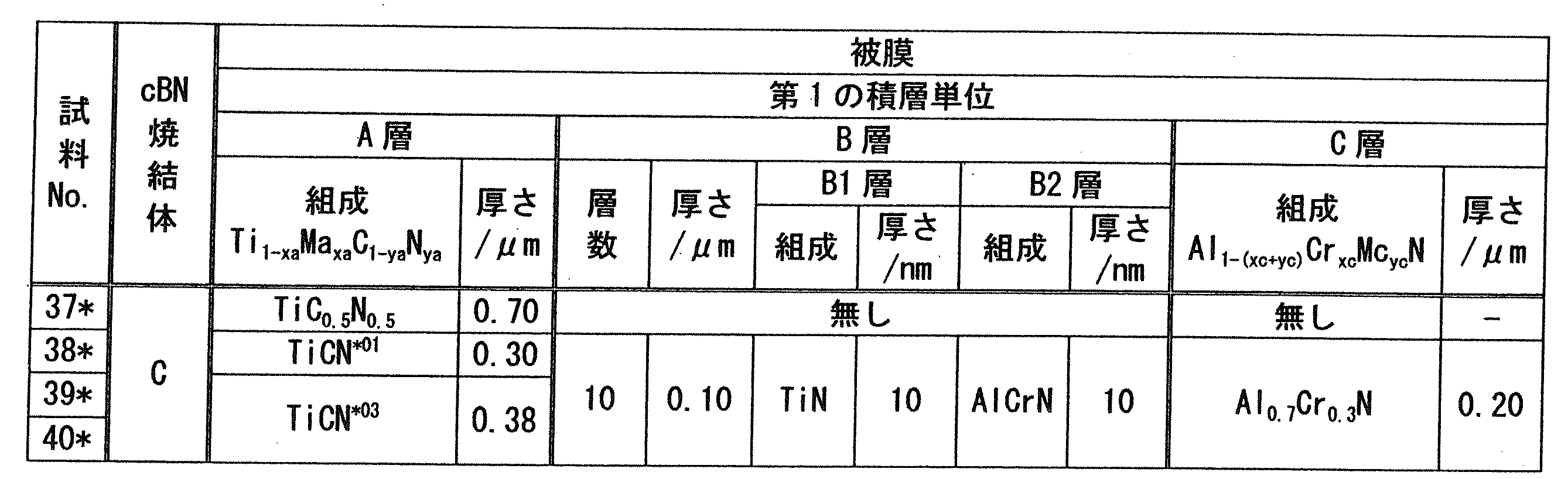
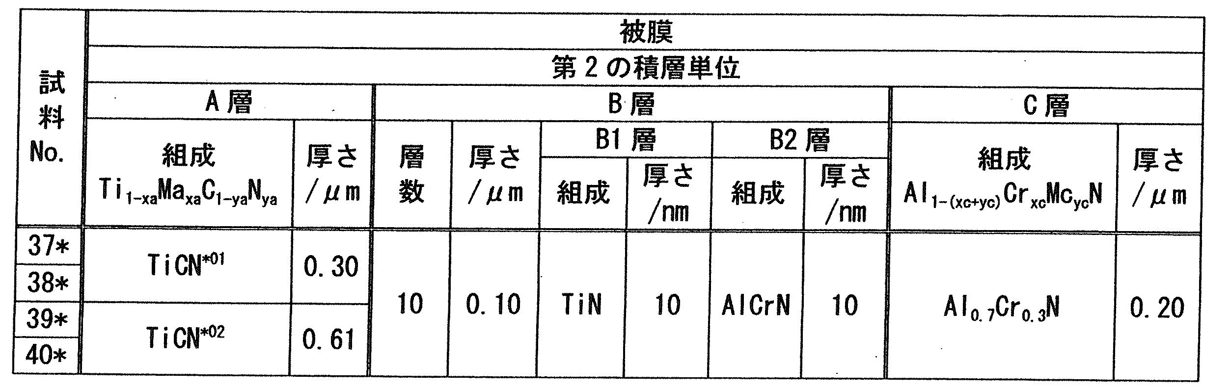


以上のようにして得られた試料No.37~No.40に係る被覆cBN工具の切削性能、仕上げ面粗さおよび面粗度寿命を実施例6と同様にして焼入鋼の連続切削により評価した。結果を表15に示す。
表12~表15に示すように、試料No.37~No.40はいずれも被膜の最表面から最も最表面側のC層までの構成は同じである。そのため3km切削した時点での耐摩耗性および加工精度はほぼ同等であった。また実施例6と同様に積層単位が多くなる程、面粗度寿命が長くなる傾向が確認された。
(試料No.41~No.46の製造)
表16~表18に示すように、cBN焼結体Aの代わりにcBN焼結体B~G用いる以外は実施例1と同様にして基材1を得、基材1上に表16~表18に示す各積層単位をこの順で積層した被膜200を形成することにより、試料No.41~No.46に係る被覆cBN工具を得た。なお各積層単位の間には密着層としてB0層(厚さ0.1μm)を形成した。

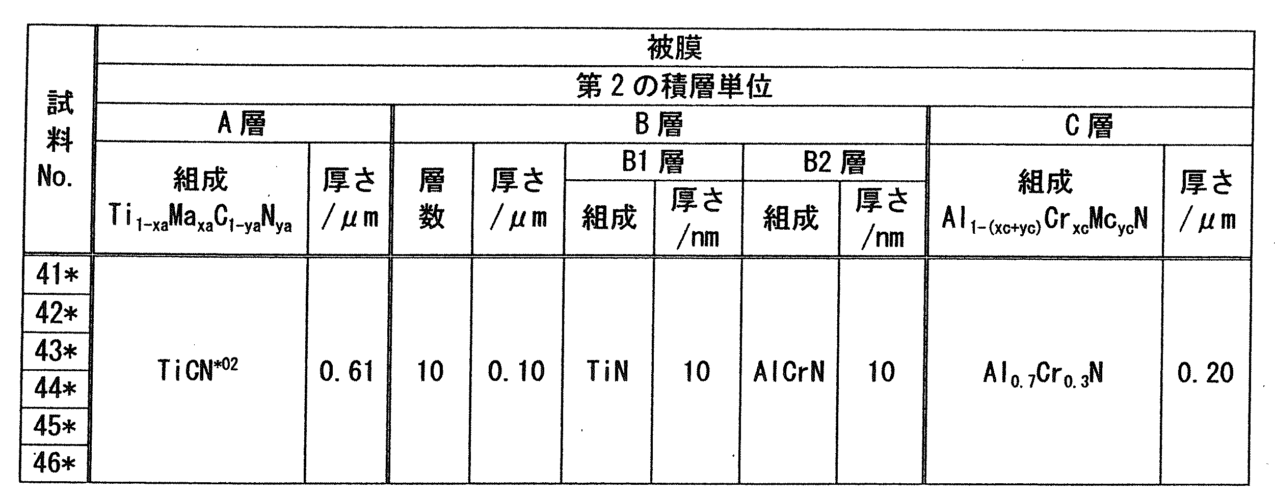
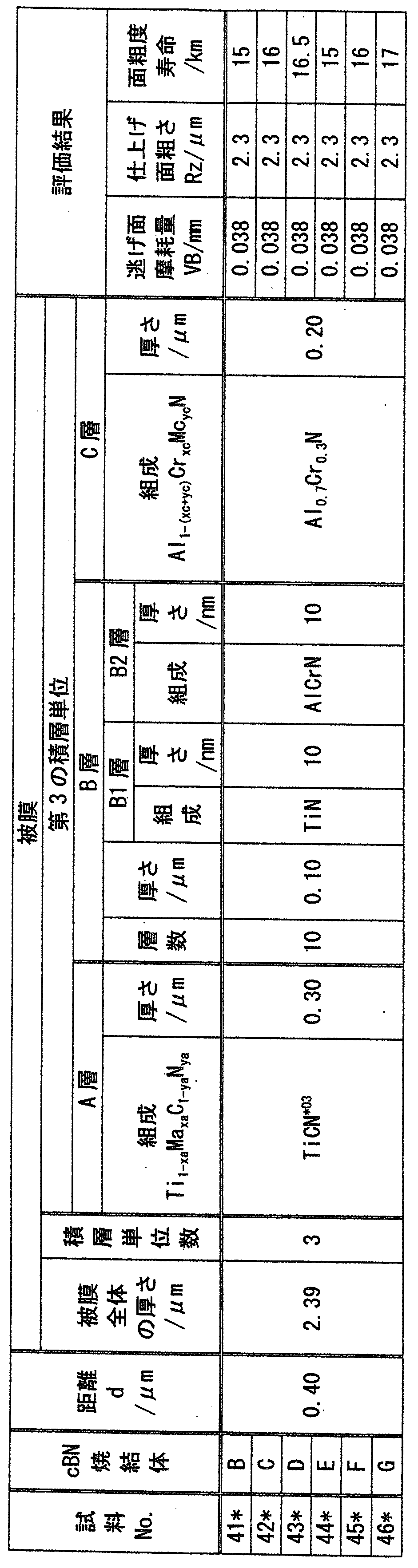
以上のようにして得られた試料No.41~No.46に係る被覆cBN工具の切削性能、仕上げ面粗さおよび面粗度寿命を実施例6と同様にして焼入鋼の連続切削により評価した。結果を表18に示す。
表16~表18に示すように試料No.41~No.46において被膜200の構成は同一であるため、3km切削した時点での耐摩耗性および加工精度はほぼ同等であった。一方、面粗度寿命については結果に差異が現れた。すなわち、cBN粒子の体積含有率が50体積%以上60体積%以下である焼結体を用いた試料は、その他の試料に比して面粗度寿命が長い結果となった。この結果は基材を構成するcBN焼結体の耐摩耗性および耐欠損性が影響したものと考えることができる。
表19~21に示すように各積層単位においてA層とC層との間にB層を形成せず、かつ各積層単位の間にB0層を形成しないことを除いては上記試料No.36と同様にして試料No.47に係る被覆cBN工具を得た。


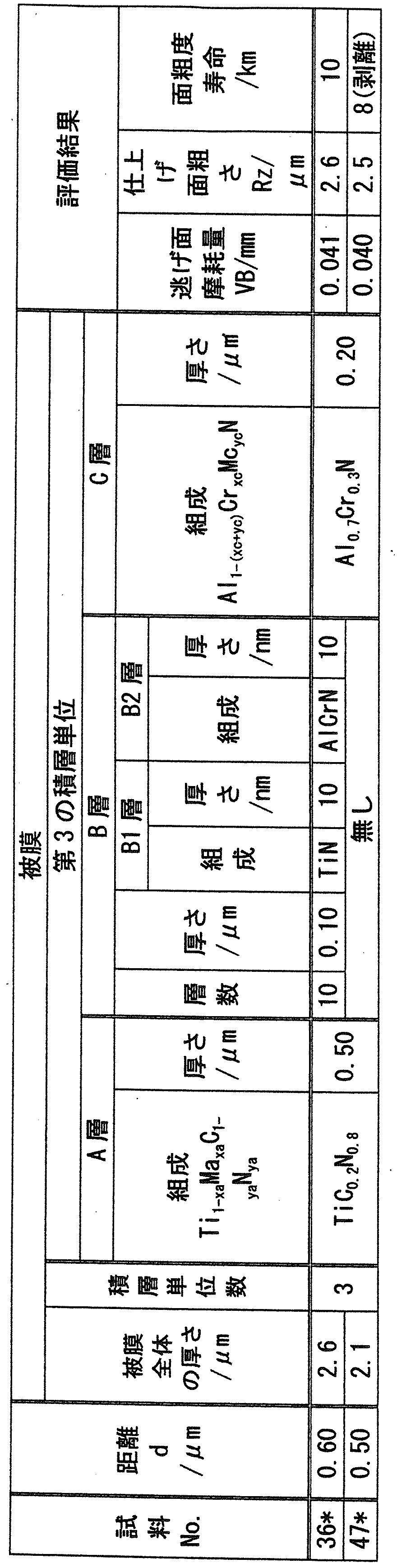
以上のようにして得られた試料No.47に係る被覆cBN工具の切削性能、仕上げ面粗さおよび面粗度寿命を実施例6と同様にして焼入鋼の連続切削により評価した。結果を表21に示す。
表19~表21に示すように、試料No.47では面粗度寿命の測定の際に剥離が発生した。この結果から各積層単位においてA層とC層との間にはB層を配置することが好ましいことが分かる。
Claims (11)
- 立方晶窒化硼素焼結体と、その上に形成された被膜とを備え、
前記被膜はA層とC層とを含み、
前記A層は、Ti1-xaMaxaC1-yaNya(ただし、MaはCr、NbおよびWの1種以上であり、xaは0≦xa≦0.7であり、yaは0≦ya≦1である)から構成され、
前記C層は、Al1-(xc+yc)CrxcMcycN(ただし、McはTi、VおよびSiの1種以上であり、xcは0.2≦xc≦0.8であり、ycは0≦yc≦0.6であり、かつxc+ycは0.2≦xc+yc≦0.8である)から構成され、
前記A層は、前記被膜の最表面または前記被膜の前記最表面と前記C層との間に形成され、
前記被膜の前記最表面と前記C層の上面との距離は、0.1μm以上1.0μm以下である、表面被覆窒化硼素焼結体工具。 - 前記被膜の前記最表面と前記C層の前記上面との距離は、0.3μm以上0.7μm以下である、請求項1に記載の表面被覆窒化硼素焼結体工具。
- 前記C層は、0.1μm以上1.0μm以下の厚さを有する、請求項1または請求項2に記載の表面被覆窒化硼素焼結体工具。
- 前記被膜は、複数の前記A層と、複数の前記C層とを含み、
前記C層の上に前記A層を有する積層単位を2つ以上含む、請求項1~請求項3のいずれか1項に記載の表面被覆窒化硼素焼結体工具。 - 前記被膜は、前記A層と前記C層との間にB層をさらに含み、
前記B層は、Al、CrおよびTiからなる群より選ばれる1種以上の元素と、Nとから構成される1種以上の化合物を含む、請求項1~請求項4のいずれか1項に記載の表面被覆窒化硼素焼結体工具。 - 前記B層は、TiNから構成されるB1層と、AlCrNから構成されるB2層とが交互にそれぞれ1層以上積層されてなる多層構造を含む、請求項5に記載の表面被覆窒化硼素焼結体工具。
- 前記B1層および前記B2層の厚さは、それぞれ0.5nm以上30nm未満である、請求項6に記載の表面被覆窒化硼素焼結体工具。
- 前記B層は、AlTiCrNから構成される化合物を含む、請求項5に記載の表面被覆窒化硼素焼結体工具。
- 前記A層は、前記yaが前記A層の厚さ方向において傾斜状またはステップ状に変化する領域を含む、請求項1~請求項8のいずれか1項に記載の表面被覆窒化硼素焼結体工具。
- 前記立方晶窒化硼素焼結体と接する層は、前記C層である、請求項1~請求項9のいずれか1項に記載の表面被覆窒化硼素焼結体工具。
- 前記被膜は、0.5μm以上10μm以下の厚さを有する、請求項1~請求項10のいずれか1項に記載の表面被覆窒化硼素焼結体工具。
Priority Applications (6)
| Application Number | Priority Date | Filing Date | Title |
|---|---|---|---|
| US15/032,976 US10030299B2 (en) | 2013-10-31 | 2014-09-19 | Surface-coated boron nitride sintered body tool |
| KR1020167011202A KR102269461B1 (ko) | 2013-10-31 | 2014-09-19 | 표면 피복 질화붕소 소결체 공구 |
| MX2016005121A MX2016005121A (es) | 2013-10-31 | 2014-09-19 | Herramienta sinterizada de nitruro de boro de superficie-revestida. |
| CA2928761A CA2928761A1 (en) | 2013-10-31 | 2014-09-19 | Surface-coated boron nitride sintered body tool |
| EP14857427.0A EP3064298B1 (en) | 2013-10-31 | 2014-09-19 | Surface-coated boron nitride sintered body tool |
| CN201480059671.3A CN105705280B (zh) | 2013-10-31 | 2014-09-19 | 表面被覆氮化硼烧结体工具 |
Applications Claiming Priority (2)
| Application Number | Priority Date | Filing Date | Title |
|---|---|---|---|
| JP2013-227077 | 2013-10-31 | ||
| JP2013227077A JP5742042B2 (ja) | 2013-10-31 | 2013-10-31 | 表面被覆窒化硼素焼結体工具 |
Publications (1)
| Publication Number | Publication Date |
|---|---|
| WO2015064241A1 true WO2015064241A1 (ja) | 2015-05-07 |
Family
ID=53003854
Family Applications (1)
| Application Number | Title | Priority Date | Filing Date |
|---|---|---|---|
| PCT/JP2014/074821 Ceased WO2015064241A1 (ja) | 2013-10-31 | 2014-09-19 | 表面被覆窒化硼素焼結体工具 |
Country Status (8)
| Country | Link |
|---|---|
| US (1) | US10030299B2 (ja) |
| EP (1) | EP3064298B1 (ja) |
| JP (1) | JP5742042B2 (ja) |
| KR (1) | KR102269461B1 (ja) |
| CN (1) | CN105705280B (ja) |
| CA (1) | CA2928761A1 (ja) |
| MX (1) | MX2016005121A (ja) |
| WO (1) | WO2015064241A1 (ja) |
Cited By (1)
| Publication number | Priority date | Publication date | Assignee | Title |
|---|---|---|---|---|
| WO2018078731A1 (ja) * | 2016-10-25 | 2018-05-03 | オーエスジー株式会社 | 硬質被膜および硬質被膜被覆部材 |
Families Citing this family (8)
| Publication number | Priority date | Publication date | Assignee | Title |
|---|---|---|---|---|
| US20180117678A1 (en) | 2016-03-30 | 2018-05-03 | Sumitomo Electric Hardmetal Corp. | Surface-coated cubic boron nitride sintered material, and cutting tool including the same |
| JP7083448B2 (ja) * | 2017-01-07 | 2022-06-13 | 株式会社タンガロイ | 被覆切削工具 |
| WO2018198421A1 (ja) | 2017-04-25 | 2018-11-01 | 住友電気工業株式会社 | 切削工具およびその製造方法 |
| US11136672B2 (en) * | 2018-08-30 | 2021-10-05 | Apple Inc. | Electronic devices having corrosion-resistant coatings |
| EP3991888B1 (en) * | 2019-10-10 | 2023-09-06 | Sumitomo Electric Hardmetal Corp. | Cutting tool |
| CN114929415B (zh) * | 2020-01-08 | 2024-10-18 | 住友电工硬质合金株式会社 | 切削工具 |
| US12050436B2 (en) | 2020-09-01 | 2024-07-30 | Apple Inc. | Bright color coatings for electronic devices |
| US12090557B1 (en) * | 2023-05-17 | 2024-09-17 | Sumitomo Electric Industries, Ltd. | Cutting tool |
Citations (5)
| Publication number | Priority date | Publication date | Assignee | Title |
|---|---|---|---|---|
| JPH09323204A (ja) * | 1996-06-05 | 1997-12-16 | Hitachi Tool Eng Ltd | 多層被覆硬質工具 |
| JP2008279563A (ja) * | 2007-05-11 | 2008-11-20 | Sumitomo Electric Ind Ltd | 表面被覆切削工具 |
| JP2009248238A (ja) * | 2008-04-04 | 2009-10-29 | Sumitomo Electric Hardmetal Corp | 表面被覆切削工具 |
| WO2010150335A1 (ja) | 2009-06-22 | 2010-12-29 | 株式会社タンガロイ | 被覆立方晶窒化硼素焼結体工具 |
| WO2012005275A1 (ja) | 2010-07-06 | 2012-01-12 | 株式会社タンガロイ | 被覆cBN焼結体工具 |
Family Cites Families (14)
| Publication number | Priority date | Publication date | Assignee | Title |
|---|---|---|---|---|
| US5330853A (en) * | 1991-03-16 | 1994-07-19 | Leybold Ag | Multilayer Ti-Al-N coating for tools |
| JP2005297141A (ja) * | 2004-04-13 | 2005-10-27 | Sumitomo Electric Hardmetal Corp | 表面被覆スローアウェイチップ |
| WO2005099945A1 (ja) | 2004-04-13 | 2005-10-27 | Sumitomo Electric Hardmetal Corp. | 表面被覆切削工具 |
| JP4672442B2 (ja) * | 2005-05-31 | 2011-04-20 | オーエスジー株式会社 | 硬質積層被膜、および硬質積層被膜被覆工具 |
| JP4950499B2 (ja) * | 2006-02-03 | 2012-06-13 | 株式会社神戸製鋼所 | 硬質皮膜およびその成膜方法 |
| EP2000237A1 (en) | 2006-03-28 | 2008-12-10 | Kyocera Corporation | Surface-coated tool |
| CN101400465A (zh) | 2006-03-28 | 2009-04-01 | 京瓷株式会社 | 表面被覆工具 |
| EP2010691B1 (de) * | 2006-04-21 | 2017-12-06 | CemeCon AG | Beschichteter körper |
| JP4883477B2 (ja) | 2006-07-14 | 2012-02-22 | 三菱マテリアル株式会社 | 高硬度鋼の高速断続切削加工ですぐれた耐欠損性を発揮する表面被覆立方晶窒化ほう素基超高圧焼結材料製切削工具 |
| JP5444709B2 (ja) | 2008-12-24 | 2014-03-19 | 新日鐵住金株式会社 | 高炉用コークスの製造方法 |
| JP5545646B2 (ja) | 2010-06-18 | 2014-07-09 | ダイハツ工業株式会社 | モータ駆動制御装置 |
| JP2012024854A (ja) * | 2010-07-20 | 2012-02-09 | Mitsubishi Materials Corp | 表面被覆切削工具 |
| CN102666437B (zh) | 2010-10-28 | 2014-03-12 | 住友电工硬质合金株式会社 | 表面被覆烧结体 |
| JP5663814B2 (ja) * | 2013-07-03 | 2015-02-04 | 住友電工ハードメタル株式会社 | 表面被覆窒化硼素焼結体工具 |
-
2013
- 2013-10-31 JP JP2013227077A patent/JP5742042B2/ja active Active
-
2014
- 2014-09-19 US US15/032,976 patent/US10030299B2/en active Active
- 2014-09-19 WO PCT/JP2014/074821 patent/WO2015064241A1/ja not_active Ceased
- 2014-09-19 MX MX2016005121A patent/MX2016005121A/es unknown
- 2014-09-19 EP EP14857427.0A patent/EP3064298B1/en active Active
- 2014-09-19 CA CA2928761A patent/CA2928761A1/en not_active Abandoned
- 2014-09-19 CN CN201480059671.3A patent/CN105705280B/zh active Active
- 2014-09-19 KR KR1020167011202A patent/KR102269461B1/ko active Active
Patent Citations (5)
| Publication number | Priority date | Publication date | Assignee | Title |
|---|---|---|---|---|
| JPH09323204A (ja) * | 1996-06-05 | 1997-12-16 | Hitachi Tool Eng Ltd | 多層被覆硬質工具 |
| JP2008279563A (ja) * | 2007-05-11 | 2008-11-20 | Sumitomo Electric Ind Ltd | 表面被覆切削工具 |
| JP2009248238A (ja) * | 2008-04-04 | 2009-10-29 | Sumitomo Electric Hardmetal Corp | 表面被覆切削工具 |
| WO2010150335A1 (ja) | 2009-06-22 | 2010-12-29 | 株式会社タンガロイ | 被覆立方晶窒化硼素焼結体工具 |
| WO2012005275A1 (ja) | 2010-07-06 | 2012-01-12 | 株式会社タンガロイ | 被覆cBN焼結体工具 |
Cited By (5)
| Publication number | Priority date | Publication date | Assignee | Title |
|---|---|---|---|---|
| WO2018078731A1 (ja) * | 2016-10-25 | 2018-05-03 | オーエスジー株式会社 | 硬質被膜および硬質被膜被覆部材 |
| CN109937268A (zh) * | 2016-10-25 | 2019-06-25 | Osg株式会社 | 硬质被膜和硬质被膜被覆构件 |
| JPWO2018078731A1 (ja) * | 2016-10-25 | 2019-09-26 | オーエスジー株式会社 | 硬質被膜および硬質被膜被覆部材 |
| US11028487B2 (en) | 2016-10-25 | 2021-06-08 | Osg Corporation | Hard coating and member coated with hard coating |
| CN109937268B (zh) * | 2016-10-25 | 2021-09-21 | Osg株式会社 | 硬质被膜和硬质被膜被覆构件 |
Also Published As
| Publication number | Publication date |
|---|---|
| CA2928761A1 (en) | 2015-05-07 |
| KR102269461B1 (ko) | 2021-06-28 |
| JP5742042B2 (ja) | 2015-07-01 |
| US10030299B2 (en) | 2018-07-24 |
| CN105705280A (zh) | 2016-06-22 |
| KR20160078972A (ko) | 2016-07-05 |
| US20160265098A1 (en) | 2016-09-15 |
| CN105705280B (zh) | 2018-07-06 |
| MX2016005121A (es) | 2016-08-03 |
| EP3064298A4 (en) | 2017-05-31 |
| JP2015085465A (ja) | 2015-05-07 |
| EP3064298A1 (en) | 2016-09-07 |
| EP3064298B1 (en) | 2020-09-02 |
Similar Documents
| Publication | Publication Date | Title |
|---|---|---|
| JP5742042B2 (ja) | 表面被覆窒化硼素焼結体工具 | |
| JP6016270B2 (ja) | 表面被覆窒化硼素焼結体工具 | |
| WO2018070195A1 (ja) | 表面被覆切削工具 | |
| JP7380978B1 (ja) | 切削工具 | |
| WO2017179233A1 (ja) | 硬質被膜および切削工具 | |
| JP6016271B2 (ja) | 表面被覆窒化硼素焼結体工具 | |
| CN105263657B (zh) | 表面被覆氮化硼烧结体工具 | |
| JP6016269B2 (ja) | 表面被覆窒化硼素焼結体工具 | |
| JP5663815B2 (ja) | 表面被覆窒化硼素焼結体工具 | |
| JP2016185589A (ja) | 表面被覆切削工具 | |
| JP6253112B2 (ja) | 表面被覆窒化硼素焼結体工具 | |
| JP7338827B1 (ja) | 切削工具 | |
| JP5663813B2 (ja) | 表面被覆窒化硼素焼結体工具 | |
| JP2015047644A (ja) | 耐摩耗性にすぐれた表面被覆切削工具 | |
| JP2015104757A (ja) | 高速切削加工で硬質被覆層がすぐれた耐摩耗性と耐チッピング性を発揮する表面被覆切削工具 | |
| JP2024005015A (ja) | 切削工具 | |
| JP2008073821A (ja) | 硬質被覆層がすぐれた耐チッピング性を発揮する表面被覆切削工具 |
Legal Events
| Date | Code | Title | Description |
|---|---|---|---|
| 121 | Ep: the epo has been informed by wipo that ep was designated in this application |
Ref document number: 14857427 Country of ref document: EP Kind code of ref document: A1 |
|
| REEP | Request for entry into the european phase |
Ref document number: 2014857427 Country of ref document: EP |
|
| WWE | Wipo information: entry into national phase |
Ref document number: MX/A/2016/005121 Country of ref document: MX Ref document number: 2014857427 Country of ref document: EP |
|
| ENP | Entry into the national phase |
Ref document number: 2928761 Country of ref document: CA |
|
| ENP | Entry into the national phase |
Ref document number: 20167011202 Country of ref document: KR Kind code of ref document: A |
|
| WWE | Wipo information: entry into national phase |
Ref document number: 15032976 Country of ref document: US |
|
| WWE | Wipo information: entry into national phase |
Ref document number: IDP00201602933 Country of ref document: ID |
|
| NENP | Non-entry into the national phase |
Ref country code: DE |