WO2015064232A1 - 半導体モジュール - Google Patents
半導体モジュール Download PDFInfo
- Publication number
- WO2015064232A1 WO2015064232A1 PCT/JP2014/074485 JP2014074485W WO2015064232A1 WO 2015064232 A1 WO2015064232 A1 WO 2015064232A1 JP 2014074485 W JP2014074485 W JP 2014074485W WO 2015064232 A1 WO2015064232 A1 WO 2015064232A1
- Authority
- WO
- WIPO (PCT)
- Prior art keywords
- metal foil
- semiconductor module
- cooler
- insulating substrate
- semiconductor
- Prior art date
- Legal status (The legal status is an assumption and is not a legal conclusion. Google has not performed a legal analysis and makes no representation as to the accuracy of the status listed.)
- Ceased
Links
Images



Classifications
-
- H—ELECTRICITY
- H10—SEMICONDUCTOR DEVICES; ELECTRIC SOLID-STATE DEVICES NOT OTHERWISE PROVIDED FOR
- H10W—GENERIC PACKAGES, INTERCONNECTIONS, CONNECTORS OR OTHER CONSTRUCTIONAL DETAILS OF DEVICES COVERED BY CLASS H10
- H10W40/00—Arrangements for thermal protection or thermal control
- H10W40/20—Arrangements for cooling
- H10W40/22—Arrangements for cooling characterised by their shape, e.g. having conical or cylindrical projections
-
- C—CHEMISTRY; METALLURGY
- C04—CEMENTS; CONCRETE; ARTIFICIAL STONE; CERAMICS; REFRACTORIES
- C04B—LIME, MAGNESIA; SLAG; CEMENTS; COMPOSITIONS THEREOF, e.g. MORTARS, CONCRETE OR LIKE BUILDING MATERIALS; ARTIFICIAL STONE; CERAMICS; REFRACTORIES; TREATMENT OF NATURAL STONE
- C04B37/00—Joining burned ceramic articles with other burned ceramic articles or other articles by heating
- C04B37/02—Joining burned ceramic articles with other burned ceramic articles or other articles by heating with metallic articles
- C04B37/021—Joining burned ceramic articles with other burned ceramic articles or other articles by heating with metallic articles in a direct manner, e.g. direct copper bonding [DCB]
-
- H—ELECTRICITY
- H10—SEMICONDUCTOR DEVICES; ELECTRIC SOLID-STATE DEVICES NOT OTHERWISE PROVIDED FOR
- H10W—GENERIC PACKAGES, INTERCONNECTIONS, CONNECTORS OR OTHER CONSTRUCTIONAL DETAILS OF DEVICES COVERED BY CLASS H10
- H10W40/00—Arrangements for thermal protection or thermal control
- H10W40/20—Arrangements for cooling
- H10W40/25—Arrangements for cooling characterised by their materials
- H10W40/255—Arrangements for cooling characterised by their materials having a laminate or multilayered structure, e.g. direct bond copper [DBC] ceramic substrates
-
- H—ELECTRICITY
- H10—SEMICONDUCTOR DEVICES; ELECTRIC SOLID-STATE DEVICES NOT OTHERWISE PROVIDED FOR
- H10W—GENERIC PACKAGES, INTERCONNECTIONS, CONNECTORS OR OTHER CONSTRUCTIONAL DETAILS OF DEVICES COVERED BY CLASS H10
- H10W40/00—Arrangements for thermal protection or thermal control
- H10W40/70—Fillings or auxiliary members in containers or in encapsulations for thermal protection or control
- H10W40/77—Auxiliary members characterised by their shape
- H10W40/778—Auxiliary members characterised by their shape in encapsulations
-
- H—ELECTRICITY
- H10—SEMICONDUCTOR DEVICES; ELECTRIC SOLID-STATE DEVICES NOT OTHERWISE PROVIDED FOR
- H10W—GENERIC PACKAGES, INTERCONNECTIONS, CONNECTORS OR OTHER CONSTRUCTIONAL DETAILS OF DEVICES COVERED BY CLASS H10
- H10W70/00—Package substrates; Interposers; Redistribution layers [RDL]
- H10W70/60—Insulating or insulated package substrates; Interposers; Redistribution layers
- H10W70/62—Insulating or insulated package substrates; Interposers; Redistribution layers characterised by their interconnections
- H10W70/65—Shapes or dispositions of interconnections
- H10W70/658—Shapes or dispositions of interconnections for devices provided for in groups H10D8/00 - H10D48/00
-
- H—ELECTRICITY
- H10—SEMICONDUCTOR DEVICES; ELECTRIC SOLID-STATE DEVICES NOT OTHERWISE PROVIDED FOR
- H10W—GENERIC PACKAGES, INTERCONNECTIONS, CONNECTORS OR OTHER CONSTRUCTIONAL DETAILS OF DEVICES COVERED BY CLASS H10
- H10W70/00—Package substrates; Interposers; Redistribution layers [RDL]
- H10W70/60—Insulating or insulated package substrates; Interposers; Redistribution layers
- H10W70/67—Insulating or insulated package substrates; Interposers; Redistribution layers characterised by their insulating layers or insulating parts
- H10W70/69—Insulating materials thereof
-
- H—ELECTRICITY
- H10—SEMICONDUCTOR DEVICES; ELECTRIC SOLID-STATE DEVICES NOT OTHERWISE PROVIDED FOR
- H10W—GENERIC PACKAGES, INTERCONNECTIONS, CONNECTORS OR OTHER CONSTRUCTIONAL DETAILS OF DEVICES COVERED BY CLASS H10
- H10W72/00—Interconnections or connectors in packages
-
- H—ELECTRICITY
- H10—SEMICONDUCTOR DEVICES; ELECTRIC SOLID-STATE DEVICES NOT OTHERWISE PROVIDED FOR
- H10W—GENERIC PACKAGES, INTERCONNECTIONS, CONNECTORS OR OTHER CONSTRUCTIONAL DETAILS OF DEVICES COVERED BY CLASS H10
- H10W90/00—Package configurations
-
- H—ELECTRICITY
- H10—SEMICONDUCTOR DEVICES; ELECTRIC SOLID-STATE DEVICES NOT OTHERWISE PROVIDED FOR
- H10W—GENERIC PACKAGES, INTERCONNECTIONS, CONNECTORS OR OTHER CONSTRUCTIONAL DETAILS OF DEVICES COVERED BY CLASS H10
- H10W90/00—Package configurations
- H10W90/401—Package configurations characterised by multiple insulating or insulated package substrates, interposers or RDLs
-
- H—ELECTRICITY
- H10—SEMICONDUCTOR DEVICES; ELECTRIC SOLID-STATE DEVICES NOT OTHERWISE PROVIDED FOR
- H10W—GENERIC PACKAGES, INTERCONNECTIONS, CONNECTORS OR OTHER CONSTRUCTIONAL DETAILS OF DEVICES COVERED BY CLASS H10
- H10W90/00—Package configurations
- H10W90/701—Package configurations characterised by the relative positions of pads or connectors relative to package parts
-
- C—CHEMISTRY; METALLURGY
- C04—CEMENTS; CONCRETE; ARTIFICIAL STONE; CERAMICS; REFRACTORIES
- C04B—LIME, MAGNESIA; SLAG; CEMENTS; COMPOSITIONS THEREOF, e.g. MORTARS, CONCRETE OR LIKE BUILDING MATERIALS; ARTIFICIAL STONE; CERAMICS; REFRACTORIES; TREATMENT OF NATURAL STONE
- C04B2237/00—Aspects relating to ceramic laminates or to joining of ceramic articles with other articles by heating
- C04B2237/30—Composition of layers of ceramic laminates or of ceramic or metallic articles to be joined by heating, e.g. Si substrates
- C04B2237/32—Ceramic
- C04B2237/36—Non-oxidic
- C04B2237/366—Aluminium nitride
-
- C—CHEMISTRY; METALLURGY
- C04—CEMENTS; CONCRETE; ARTIFICIAL STONE; CERAMICS; REFRACTORIES
- C04B—LIME, MAGNESIA; SLAG; CEMENTS; COMPOSITIONS THEREOF, e.g. MORTARS, CONCRETE OR LIKE BUILDING MATERIALS; ARTIFICIAL STONE; CERAMICS; REFRACTORIES; TREATMENT OF NATURAL STONE
- C04B2237/00—Aspects relating to ceramic laminates or to joining of ceramic articles with other articles by heating
- C04B2237/30—Composition of layers of ceramic laminates or of ceramic or metallic articles to be joined by heating, e.g. Si substrates
- C04B2237/40—Metallic
- C04B2237/407—Copper
-
- H—ELECTRICITY
- H10—SEMICONDUCTOR DEVICES; ELECTRIC SOLID-STATE DEVICES NOT OTHERWISE PROVIDED FOR
- H10W—GENERIC PACKAGES, INTERCONNECTIONS, CONNECTORS OR OTHER CONSTRUCTIONAL DETAILS OF DEVICES COVERED BY CLASS H10
- H10W40/00—Arrangements for thermal protection or thermal control
- H10W40/40—Arrangements for thermal protection or thermal control involving heat exchange by flowing fluids
- H10W40/47—Arrangements for thermal protection or thermal control involving heat exchange by flowing fluids by flowing liquids, e.g. forced water cooling
-
- H—ELECTRICITY
- H10—SEMICONDUCTOR DEVICES; ELECTRIC SOLID-STATE DEVICES NOT OTHERWISE PROVIDED FOR
- H10W—GENERIC PACKAGES, INTERCONNECTIONS, CONNECTORS OR OTHER CONSTRUCTIONAL DETAILS OF DEVICES COVERED BY CLASS H10
- H10W70/00—Package substrates; Interposers; Redistribution layers [RDL]
- H10W70/40—Leadframes
- H10W70/479—Leadframes on or in insulating or insulated package substrates, interposers, or redistribution layers
Definitions
- the present invention relates to a semiconductor module in which the cooling capacity is improved in a semiconductor module using a pin junction.
- the semiconductor module of the following patent documents 1 and 2 is known as literature about a semiconductor module which improved cooling capacity.
- Patent Document 1 discloses a structure in which a semiconductor chip and a metal plate are provided between insulating substrates in which metal foils are disposed on both sides, and the outside of each insulating substrate is joined to a cooler.
- Patent Document 2 a semiconductor chip and a lead electrode are provided between insulating substrates in which metal foils are disposed on both sides, and a copper base is disposed on the outer side of each insulating substrate, and further on the outer side of each copper base (heat sink). Discloses a structure in which a heat sink (cooler) is disposed.
- Patent Document 3 is known as a document disclosing a semiconductor module using a pin junction. Patent Document 3 discloses a structure in which a semiconductor chip and a printed circuit board are connected by implant pins.
- Patent Document 1 has a problem that a thermal stress is applied between the wire and the electrode bonded to the wire when the semiconductor element is energized, and the wire is easily peeled off from the electrode due to repeated on-off for a long time.
- Patent Document 2 replaces the wire electrode of Patent Document 1 with a lead electrode, the peeling phenomenon may occur in the same manner.
- Patent Document 3 discloses a semiconductor module having a pin junction structure conceived as a countermeasure for suppressing the above-mentioned peeling phenomenon.
- the cooling surface of the semiconductor element is only on one side, the cooling capacity is low, and it is difficult to increase the power consumption.
- an object of the present invention is to provide a semiconductor module having an improved cooling capability in a semiconductor module using a pin junction.
- the semiconductor module of the present invention comprises a semiconductor element, a pin electrically and thermally connected to the top surface of the semiconductor element, an insulating substrate for pin wiring, and a back surface of the insulating substrate for pin wiring.
- a pin wiring board comprising the first metal foil arranged, and the second metal foil arranged on the front surface of the insulating substrate for pin wiring, wherein the first metal foil and the pin are joined;
- the foil includes a first DCB substrate joined to the lower surface of the semiconductor element, a first cooler thermally connected to the fourth metal foil, and a second thermally connected to the second metal foil. And a cooler.
- a second ceramic insulating substrate, a fifth metal foil disposed on the back surface of the second ceramic insulating substrate, and a sixth disposed on the front surface of the second ceramic insulating substrate It is preferable that a second DCB substrate provided with a metal foil is provided, and a second DCB substrate be disposed between the second metal foil and the second cooler and thermally connected.
- a heat spreader be disposed and thermally connected between the second metal foil and the second cooler.
- a plurality of sets of the semiconductor element and the pins can be provided.
- the input terminal and the output terminal of the semiconductor element can be derived to the outside from between the first cooler and the second cooler.
- the semiconductor module unit in which the semiconductor module is one unit, has a plurality of side-by-side faces of the semiconductor element where the input terminal and the output terminal are not exposed. It is characterized by being arranged.
- the first cooler and the second cooler are integrated so as to cover the entire row of the module units.
- heat is applied to the first cooler of the semiconductor module and the surface thermally connected to the first cooler, and the second cooler and the second cooler of the semiconductor module. It is preferable that it seal
- the pin wiring substrate electrically connected to the surface of the semiconductor element through the pins functions as a heat spreader for widening the heat transfer area since it is also thermally connected to the semiconductor element. Much heat can also be transferred from the top of the semiconductor module. By using two coolers to cool the semiconductor module from the top and bottom, the cooling capacity can be increased to provide a high-power semiconductor module.
- the semiconductor module which concerns on the 1st Embodiment of this invention WHEREIN: It is a cross-sectional schematic diagram of a semiconductor module provided with a 2 or more semiconductor element. It is a cross-sectional schematic diagram of the semiconductor module concerning the 2nd Embodiment of this invention. It is a perspective view of the semiconductor module concerning a 3rd embodiment of the present invention.
- FIG. 1 is a schematic cross-sectional view of a semiconductor module 100 according to a first embodiment of the present invention.
- the semiconductor module 100 includes the semiconductor element 1, the first DCB substrate 2, the first ceramic insulating substrate 2a, the third metal foil 2b, the fourth metal foil 2c, the solder 3a, the solder 3b, the solder 3c, the solder 3d, the solder 3e, and the second DCB.
- the semiconductor device 1 is not particularly limited, but may be, for example, an IGBT (Insulated Gate Bipolar Transistor), a power MOSFET (Metal Oxide Semiconductor Field Effect Transistor) or an FWD (Free Wheeling Diode), and these may be one semiconductor device.
- IGBT Insulated Gate Bipolar Transistor
- MOSFET Metal Oxide Semiconductor Field Effect Transistor
- FWD Free Wheeling Diode
- RB-IGBTs Reverse Blocking-Insulated Gate Bipolar Transistors
- RC-IGBTs Reverse Conducting-Insulated Gate Bipolar Transistors
- the pin wiring substrate 5 includes an insulating substrate 5a for pin wiring, a first metal foil (circuit layer) 5b, and a second metal foil 5c, and is disposed such that the first metal foil (circuit layer) 5b faces the semiconductor element 1. It is done.
- the pin wiring insulating substrate 5a is not particularly limited, but a material having a low dielectric constant and a high thermal conductivity is preferable. For example, Si 3 N 4 , AlN, or Al 2 O 3 can be used.
- the first metal foil (circuit layer) 5b and the second metal foil 5c are not particularly limited, but materials having low electrical resistance and high thermal conductivity are preferable, and copper, for example, can be used.
- the pin 10 is not particularly limited, but a metal having a low electrical resistance and a high thermal conductivity, specifically copper, is preferable.
- One end of the pin 10 is soldered to the upper surface of the semiconductor element 1 by the solder 3c, and the other end is bonded to the first metal foil (circuit layer) 5b.
- the heat generated in the semiconductor element 1 can be transferred to the first metal foil 5b, the pin wiring insulating substrate 5a, and the first metal foil 5c through the pins 10, and the pin wiring substrate 5 transfers heat.
- the heat spreader functions as an area-wide heat spreader, and the cooling efficiency of the semiconductor module 100 can be enhanced.
- the first DCB substrate 2 is composed of the first ceramic insulating substrate 2a, the third metal foil 2b and the fourth metal foil 2c, and the third metal foil 2b is disposed on the front surface of the first ceramic insulating substrate 2a.
- the fourth metal foil 2c is disposed on the back surface of the ceramic insulating substrate 2a.
- the third metal foil 2 b of the first DCB substrate 2 is bonded to the lower surface of the semiconductor element 1.
- DCB is an abbreviation of Direct Copper Bonding, and a metal foil such as copper is directly bonded to a ceramic insulating substrate. Because the ceramic insulating substrate 2a is insulating, the third metal foil 2b and the fourth metal foil 2c are electrically insulated.
- the material of the ceramic insulating substrate 2a is not particularly limited, but is preferably a material having a high thermal conductivity, and for example, AlN can be used.
- the lower surface of the semiconductor element 1 and the third metal foil 2b are electrically and thermally connected by the solder 3a.
- the third metal foil 2b and the fourth metal foil 2c are electrically insulated by the first ceramic insulating substrate 2a, the heat conduction therebetween is good.
- the fourth metal foil 2c of the first DCB substrate 2 and the outer wall of the first cooler 6 are connected by solder 3b.
- the second DCB substrate 4 is disposed between the pin wiring substrate 5 and the second cooler 7.
- the second DCB substrate 4 includes the second ceramic insulating substrate 4a, the fifth metal foil 4b, and the sixth metal foil 4c.
- the fifth metal foil 4b is disposed on the back surface of the second ceramic insulating substrate 4a.
- a sixth metal foil is disposed on the front surface of 4a.
- the second metal foil 5c of the pin wiring substrate 5 is electrically and thermally connected to the fifth metal foil 4b of the second DCB substrate 4 by the solder 3d.
- the fifth metal foil 4b and the sixth metal foil 4c of the second DCB substrate 4 are electrically insulated by the second ceramic insulating substrate 4a, the heat conduction therebetween is good.
- the sixth metal foil 4c of the second DCB substrate 4 and the outer wall of the second cooler 7 are connected by solder 3e.
- the heat generated from the semiconductor element is transferred from the lower surface of the semiconductor element 1 to the first cooler 6 through the first DCB substrate 2 and the pin connected to the upper surface of the semiconductor element 1
- the heat can be transferred to the pin wiring substrate 5 via 10 and then transferred to the second DCB substrate 4 and further transferred to the second cooler 7.
- the pin wiring substrate 5 not only functions as a wiring substrate but also plays a role as a heat spreader for widening the heat transfer area, but the second DCB substrate 4 can further disperse the heat flow to prevent the generation of hot spots.
- the semiconductor module is not limited to the one having one semiconductor element 1 but may have a structure having a plurality of sets of the semiconductor element 1 and the pins 10.
- FIG. 2 shows a schematic cross-sectional view of a semiconductor module 101 provided with two semiconductor elements 1 in a longitudinal structure according to a second embodiment of the present invention.
- the semiconductor module can double the rated output of the semiconductor module by arranging the semiconductor elements 1 in parallel connection.
- the types of the plurality of semiconductor elements 1 may be changed to different types of semiconductor elements. For example, IGBT and FWD can be connected in parallel to provide a protection effect against back electromotive force.
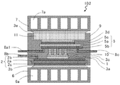
- FIG. 3 is a schematic cross-sectional view of a semiconductor module 102 according to a second embodiment of the present invention.
- the semiconductor module 102 includes the semiconductor element 1, the first DCB substrate 2, the first ceramic insulating substrate 2 a, the third metal foil 2 b, the fourth metal foil 2 c, the solder 3 a, the solder 3 b, the solder 3 c, the solder 3 d, the solder 3 e, the heat spreader 11.
- the heat spreader 11 is disposed between the pin wiring substrate 5 and the second cooler 7.
- a material of the heat spreader 11 a metal having high thermal conductivity is used, and it is desirable to use, for example, copper.
- the thickness of the heat spreader 11 is designed in accordance with the calorific value of the semiconductor element 1 and the margin of the heat generation amount generated transiently and the cooling capacity of the second cooler 7.
- the second metal foil 5c of the pin wiring substrate 5 is electrically and thermally connected to the heat spreader 11 by the solder 3d. Furthermore, the heat spreader 11 and the outer wall of the second cooler 7 are connected by solder 3e.
- the heat generated from the semiconductor element is transferred from the lower surface of the semiconductor element 1 to the first cooler 6 through the first DCB substrate 2 and the pin connected to the upper surface of the semiconductor element 1
- the heat can be transferred to the pin wiring substrate 5 through 10, then to the heat spreader 11, and further to the second cooler 7.
- the pin wiring substrate 5 not only functions as a substrate for wiring but also plays a role as a heat spreader for widening the heat transfer area.
- the heat spreader 11 uses a metal with good heat conductivity, the heat flow is further dispersed and hot It is possible to prevent the occurrence of spots.
- a printed substrate made of glass fiber epoxy resin may be used.
- the thermal resistance of the heat transfer path from the semiconductor element 1 to the second cooler 7 is low, and the temperature increase due to transient heat is also suppressed by the buffer action by the heat capacity of the heat spreader. Are better.
- a plurality of the semiconductor modules described in the first and second embodiments are arranged side by side with the side surfaces where the input terminal and the output terminal are not exposed. It can be structured.
- the first cooler 6 and the second cooler 7 can be integrated so as to cover the entire row of the semiconductor modules.
- FIG. 4 shows a perspective view of a semiconductor module 103 according to a fourth embodiment of the present invention in which a plurality of three semiconductor modules are arranged in a horizontal row.
- the first cooler 6 and the second cooler 7 are integrated with each other.
- the first cooler 6 is provided with a refrigerant inlet 6 b and a refrigerant outlet 6 c.
- the second cooler 7 is provided with a refrigerant inlet 7 b and a refrigerant outlet 7 c. It is preferable that the refrigerant flows in the first cooler 6 and the second cooler 7 in opposite directions. In this way, the semiconductor module 103 can be cooled efficiently.
Landscapes
- Chemical & Material Sciences (AREA)
- Engineering & Computer Science (AREA)
- Ceramic Engineering (AREA)
- Materials Engineering (AREA)
- Structural Engineering (AREA)
- Organic Chemistry (AREA)
- Cooling Or The Like Of Semiconductors Or Solid State Devices (AREA)
Abstract
Description
まず、本発明に係る第1の実施形態について説明する。
次に、本発明に係る第2の実施形態について説明する。
次に、本発明に係る第3の実施形態について説明する。
2 第1DCB基板
2a 第1セラミック絶縁基板
2b 第3金属箔
2c 第4金属箔
3a ハンダ
3b ハンダ
3c ハンダ
3d ハンダ
3e ハンダ
4 第2DCB基板
4a 第2セラミック絶縁基板
4b 第5金属箔
4c 第6金属箔
5 ピン配線基板
5a ピン配線用絶縁基板
5b 第1金属箔(回路層)
5c 第2金属箔
6 第1冷却器
6a 冷媒通路
6b 冷媒入口
6c 冷媒出口
7 第2冷却器
7a 冷媒通路
7b 冷媒入口
7c 冷媒出口
8a 端子
8a1 端子
8b 端子
8c 端子
9 封止樹脂
10 ピン
11 ヒートスプレッダ
100 半導体モジュール
101 半導体モジュール
102 半導体モジュール
103 半導体モジュール
Claims (8)
- 半導体素子と、
前記半導体素子の上面に電気的および熱的に接続されたピンと、
ピン配線用絶縁基板、前記ピン配線用絶縁基板の裏面に配置した第1金属箔、および前記ピン配線用絶縁基板のおもて面に配置した第2金属箔を備えており、かつ前記第1金属箔と前記ピンとが接合しているピン配線基板と、
第1セラミック絶縁基板、前記第1セラミック絶縁基板のおもて面に配置した第3金属箔、および前記第1セラミック絶縁基板の裏面に配置した第4金属箔を備えており、前記第3金属箔は、前記半導体素子の下面に接合されている第1DCB基板と、
前記第4金属箔に熱的に接続された第1冷却器と、
前記第2金属箔に熱的に接続された第2冷却器と、
を備えることを特徴とする半導体モジュール。 - 第2セラミック絶縁基板、前記第2セラミック絶縁基板の裏面に配置した第5金属箔、および前記第2セラミック絶縁基板のおもて面に配置した第6金属箔を備えた第2DCB基板を備え、
前記第2金属箔と前記第2冷却器との間に第2DCB基板を配置して熱的に接続されている請求項1に記載の半導体モジュール。 - 前記第2金属箔と前記第2冷却器との間にヒートスプレッダを配置して熱的に接続されていることを特徴とする請求項1に記載の半導体モジュール。
- 前記半導体素子および前記ピンの組を複数備えている請求項1~3のいずれか1項に記載の半導体モジュール。
- 前記半導体素子の入力端子および出力端子は、前記第1冷却器と前記第2冷却器との間から外部に導出されている請求項1~4のいずれか1項に記載の半導体モジュール。
- 請求項1~5のいずれか1項に記載の半導体モジュールを1単位とする、半導体モジュールユニットが、前記半導体素子の入力端子および出力端子が出ていない側面を対面させて、横一列に複数並べられていることを特徴とする半導体モジュール。
- 前記第1冷却器および第2冷却器はそれぞれ前記モジュールユニットの列全体を覆うように一体になっていることを特徴とする請求項6に記載の半導体モジュール。
- 前記半導体モジュールの前記第1冷却器および前記第1冷却器に熱的に接続される面と、
前記半導体モジュールの前記第2冷却器および前記第2冷却器に熱的に接続される面と、
を除いて封止樹脂で封止されている請求項1~7のいずれか1項に記載の半導体モジュール。
Priority Applications (4)
| Application Number | Priority Date | Filing Date | Title |
|---|---|---|---|
| DE112014002061.3T DE112014002061T5 (de) | 2013-10-29 | 2014-09-17 | Halbleitermodul |
| JP2015544859A JP6217756B2 (ja) | 2013-10-29 | 2014-09-17 | 半導体モジュール |
| CN201480026418.8A CN105264658A (zh) | 2013-10-29 | 2014-09-17 | 半导体模块 |
| US14/937,383 US9460981B2 (en) | 2013-10-29 | 2015-11-10 | Semiconductor module |
Applications Claiming Priority (2)
| Application Number | Priority Date | Filing Date | Title |
|---|---|---|---|
| JP2013-224424 | 2013-10-29 | ||
| JP2013224424 | 2013-10-29 |
Related Child Applications (1)
| Application Number | Title | Priority Date | Filing Date |
|---|---|---|---|
| US14/937,383 Continuation US9460981B2 (en) | 2013-10-29 | 2015-11-10 | Semiconductor module |
Publications (1)
| Publication Number | Publication Date |
|---|---|
| WO2015064232A1 true WO2015064232A1 (ja) | 2015-05-07 |
Family
ID=53003845
Family Applications (1)
| Application Number | Title | Priority Date | Filing Date |
|---|---|---|---|
| PCT/JP2014/074485 Ceased WO2015064232A1 (ja) | 2013-10-29 | 2014-09-17 | 半導体モジュール |
Country Status (5)
| Country | Link |
|---|---|
| US (1) | US9460981B2 (ja) |
| JP (1) | JP6217756B2 (ja) |
| CN (1) | CN105264658A (ja) |
| DE (1) | DE112014002061T5 (ja) |
| WO (1) | WO2015064232A1 (ja) |
Cited By (1)
| Publication number | Priority date | Publication date | Assignee | Title |
|---|---|---|---|---|
| KR20180066133A (ko) * | 2015-10-07 | 2018-06-18 | 세람테크 게엠베하 | 양측들에서 냉각되는 회로 |
Families Citing this family (19)
| Publication number | Priority date | Publication date | Assignee | Title |
|---|---|---|---|---|
| US10600718B1 (en) * | 2014-12-03 | 2020-03-24 | Ii-Vi Delaware, Inc. | Heat sink package |
| US10403601B2 (en) | 2016-06-17 | 2019-09-03 | Fairchild Semiconductor Corporation | Semiconductor package and related methods |
| FR3054928B1 (fr) * | 2016-08-05 | 2018-08-17 | Commissariat A L'energie Atomique Et Aux Energies Alternatives | Procede d'encapsulation d'un circuit integre pour former un module de puissance tridimensionnel |
| KR101905995B1 (ko) | 2016-11-09 | 2018-10-10 | 현대자동차주식회사 | 양면냉각형 파워모듈 |
| KR20190137086A (ko) * | 2017-04-06 | 2019-12-10 | 세람테크 게엠베하 | 2개의 측들 상에서 냉각되는 회로 |
| CN107634051A (zh) * | 2017-08-30 | 2018-01-26 | 扬州国扬电子有限公司 | 一种具有交叉排列电极组合的功率模组 |
| CN107393901B (zh) * | 2017-08-30 | 2023-10-13 | 扬州国扬电子有限公司 | 一种叠层基板的双面散热功率模块 |
| CN107634052A (zh) * | 2017-08-30 | 2018-01-26 | 扬州国扬电子有限公司 | 一种平行安装电极组合及功率模块 |
| CN107403780A (zh) * | 2017-08-30 | 2017-11-28 | 扬州国扬电子有限公司 | 一种交叉排列电极组合及功率模块 |
| CN107369657B (zh) * | 2017-08-30 | 2023-10-13 | 扬州国扬电子有限公司 | 一种多区域并列排布的双面散热功率模块 |
| EP3557614A1 (de) * | 2018-04-17 | 2019-10-23 | Siemens Aktiengesellschaft | Leistungsmodul mit einem leistungselektronischen bauelement auf einer substratplatte und leistungselektronische schaltung mit einem solchen leistungsmodul |
| CN108718491A (zh) * | 2018-07-24 | 2018-10-30 | 甘旭 | 多层功率器件堆叠结构 |
| CN111341762A (zh) * | 2018-12-19 | 2020-06-26 | 江苏宏微科技股份有限公司 | 一种用于大功率多管芯封装结构 |
| JP7200825B2 (ja) * | 2019-05-15 | 2023-01-10 | 株式会社デンソー | 半導体装置 |
| WO2021003539A1 (pt) * | 2019-07-09 | 2021-01-14 | Anflor Juliano | Aperfeiçoamento em acoplamento térmico entre transistor e drivers de audio com dissipador de calor |
| IT201900013743A1 (it) * | 2019-08-01 | 2021-02-01 | St Microelectronics Srl | Dispositivo elettronico di potenza incapsulato, in particolare circuito a ponte comprendente transistori di potenza, e relativo procedimento di assemblaggio |
| CN110707055B (zh) * | 2019-09-11 | 2021-12-28 | 长江存储科技有限责任公司 | 芯片、电子设备 |
| JP7638193B2 (ja) * | 2021-10-26 | 2025-03-03 | 三菱電機株式会社 | 半導体装置および電力変換装置 |
| CN115334748A (zh) * | 2022-08-10 | 2022-11-11 | 臻驱科技(上海)有限公司 | 一种低杂感功率模块及具有该低杂感功率模块的电动汽车 |
Citations (3)
| Publication number | Priority date | Publication date | Assignee | Title |
|---|---|---|---|---|
| JP2005093593A (ja) * | 2003-09-16 | 2005-04-07 | Denso Corp | 半導体冷却ユニット |
| JP2007251076A (ja) * | 2006-03-20 | 2007-09-27 | Hitachi Ltd | パワー半導体モジュール |
| JP2009064852A (ja) * | 2007-09-05 | 2009-03-26 | Okutekku:Kk | 半導体装置及び半導体装置の製造方法 |
Family Cites Families (11)
| Publication number | Priority date | Publication date | Assignee | Title |
|---|---|---|---|---|
| US6232151B1 (en) * | 1999-11-01 | 2001-05-15 | General Electric Company | Power electronic module packaging |
| JP2001308245A (ja) * | 2000-04-25 | 2001-11-02 | Denso Corp | 冷媒冷却型両面冷却半導体装置 |
| JP4958735B2 (ja) * | 2007-11-01 | 2012-06-20 | 株式会社日立製作所 | パワー半導体モジュールの製造方法、パワー半導体モジュールの製造装置、パワー半導体モジュール、及び接合方法 |
| WO2009125779A1 (ja) | 2008-04-09 | 2009-10-15 | 富士電機デバイステクノロジー株式会社 | 半導体装置及び半導体装置の製造方法 |
| WO2011083737A1 (ja) | 2010-01-05 | 2011-07-14 | 富士電機システムズ株式会社 | 半導体装置用ユニットおよび半導体装置 |
| DE202010017532U1 (de) * | 2010-03-16 | 2012-01-19 | Eppsteinfoils Gmbh & Co.Kg | Foliensystem für LED-Anwendungen |
| WO2013118415A1 (ja) * | 2012-02-09 | 2013-08-15 | 富士電機株式会社 | 半導体装置 |
| JP5915350B2 (ja) * | 2012-04-19 | 2016-05-11 | 富士電機株式会社 | パワー半導体モジュール |
| CN104205301B (zh) * | 2012-08-17 | 2017-10-10 | 富士电机株式会社 | 电子元器件及电子元器件的制造方法 |
| KR101402989B1 (ko) * | 2013-06-12 | 2014-06-11 | 한국과학기술연구원 | 기판과의 결합력이 향상된 탄소나노튜브 기반 전계효과트랜지스터 소자의 제조방법 및 이에 의하여 제조된 탄소나노튜브 기반 전계효과트랜지스터 소자 |
| DE112014001491T5 (de) * | 2013-10-30 | 2015-12-10 | Fuji Electric Co., Ltd. | Halbleitermodul |
-
2014
- 2014-09-17 JP JP2015544859A patent/JP6217756B2/ja not_active Expired - Fee Related
- 2014-09-17 CN CN201480026418.8A patent/CN105264658A/zh active Pending
- 2014-09-17 DE DE112014002061.3T patent/DE112014002061T5/de not_active Withdrawn
- 2014-09-17 WO PCT/JP2014/074485 patent/WO2015064232A1/ja not_active Ceased
-
2015
- 2015-11-10 US US14/937,383 patent/US9460981B2/en not_active Expired - Fee Related
Patent Citations (3)
| Publication number | Priority date | Publication date | Assignee | Title |
|---|---|---|---|---|
| JP2005093593A (ja) * | 2003-09-16 | 2005-04-07 | Denso Corp | 半導体冷却ユニット |
| JP2007251076A (ja) * | 2006-03-20 | 2007-09-27 | Hitachi Ltd | パワー半導体モジュール |
| JP2009064852A (ja) * | 2007-09-05 | 2009-03-26 | Okutekku:Kk | 半導体装置及び半導体装置の製造方法 |
Cited By (3)
| Publication number | Priority date | Publication date | Assignee | Title |
|---|---|---|---|---|
| KR20180066133A (ko) * | 2015-10-07 | 2018-06-18 | 세람테크 게엠베하 | 양측들에서 냉각되는 회로 |
| JP2018531516A (ja) * | 2015-10-07 | 2018-10-25 | セラムテック ゲゼルシャフト ミット ベシュレンクテル ハフツングCeramTec GmbH | 二面冷却式回路 |
| KR102541854B1 (ko) * | 2015-10-07 | 2023-06-08 | 세람테크 게엠베하 | 양측들에서 냉각되는 회로 |
Also Published As
| Publication number | Publication date |
|---|---|
| DE112014002061T5 (de) | 2016-01-07 |
| CN105264658A (zh) | 2016-01-20 |
| US20160064302A1 (en) | 2016-03-03 |
| US9460981B2 (en) | 2016-10-04 |
| JPWO2015064232A1 (ja) | 2017-03-09 |
| JP6217756B2 (ja) | 2017-10-25 |
Similar Documents
| Publication | Publication Date | Title |
|---|---|---|
| JP6217756B2 (ja) | 半導体モジュール | |
| JP6037045B2 (ja) | 半導体モジュール | |
| US11139278B2 (en) | Low parasitic inductance power module and double-faced heat-dissipation low parasitic inductance power module | |
| JP5627499B2 (ja) | 半導体モジュールを備えた半導体装置 | |
| CN105103286B (zh) | 半导体模块 | |
| JP5538653B2 (ja) | ヒートシンクおよび当該ヒートシンクを備えた半導体装置 | |
| JP4803241B2 (ja) | 半導体モジュール | |
| CN105161477B (zh) | 一种平面型功率模块 | |
| JP6330436B2 (ja) | パワー半導体モジュール | |
| CN110047807A (zh) | 半导体装置 | |
| CN108417546B (zh) | 电力电子模块 | |
| JP2014127538A (ja) | 半導体モジュール | |
| KR20170024254A (ko) | 파워 반도체 모듈 및 이의 제조 방법 | |
| JP2011211017A (ja) | 半導体モジュールおよびそれを備えた半導体装置 | |
| JP5402778B2 (ja) | 半導体モジュールを備えた半導体装置 | |
| JP2009117701A (ja) | パワーモジュール | |
| JP2009021445A (ja) | インバータ装置 | |
| JP7012453B2 (ja) | ブリッジレッグ回路組立品およびフルブリッジ回路組立品 | |
| JP2011176087A (ja) | 半導体モジュール、及び電力変換装置 | |
| KR101897304B1 (ko) | 파워 모듈 | |
| CN104733404A (zh) | 半导体装置 | |
| KR100705354B1 (ko) | 열전모듈 냉각부 가이드 | |
| JP5494576B2 (ja) | 半導体モジュール | |
| WO2023203688A1 (ja) | 半導体装置および半導体装置の製造方法 | |
| CN121793223A (zh) | 一种功率模块效率增强方法 |
Legal Events
| Date | Code | Title | Description |
|---|---|---|---|
| WWE | Wipo information: entry into national phase |
Ref document number: 201480026418.8 Country of ref document: CN |
|
| 121 | Ep: the epo has been informed by wipo that ep was designated in this application |
Ref document number: 14857732 Country of ref document: EP Kind code of ref document: A1 |
|
| ENP | Entry into the national phase |
Ref document number: 2015544859 Country of ref document: JP Kind code of ref document: A |
|
| WWE | Wipo information: entry into national phase |
Ref document number: 112014002061 Country of ref document: DE Ref document number: 1120140020613 Country of ref document: DE |
|
| 122 | Ep: pct application non-entry in european phase |
Ref document number: 14857732 Country of ref document: EP Kind code of ref document: A1 |