WO2015053128A1 - ボンディングワイヤ用銅素線、及びボンディングワイヤ用銅素線の製造方法 - Google Patents
ボンディングワイヤ用銅素線、及びボンディングワイヤ用銅素線の製造方法 Download PDFInfo
- Publication number
- WO2015053128A1 WO2015053128A1 PCT/JP2014/075999 JP2014075999W WO2015053128A1 WO 2015053128 A1 WO2015053128 A1 WO 2015053128A1 JP 2014075999 W JP2014075999 W JP 2014075999W WO 2015053128 A1 WO2015053128 A1 WO 2015053128A1
- Authority
- WO
- WIPO (PCT)
- Prior art keywords
- wire
- bonding
- copper
- strand
- purity
- Prior art date
- Legal status (The legal status is an assumption and is not a legal conclusion. Google has not performed a legal analysis and makes no representation as to the accuracy of the status listed.)
- Ceased
Links
Images
Classifications
-
- C—CHEMISTRY; METALLURGY
- C22—METALLURGY; FERROUS OR NON-FERROUS ALLOYS; TREATMENT OF ALLOYS OR NON-FERROUS METALS
- C22C—ALLOYS
- C22C9/00—Alloys based on copper
-
- C—CHEMISTRY; METALLURGY
- C22—METALLURGY; FERROUS OR NON-FERROUS ALLOYS; TREATMENT OF ALLOYS OR NON-FERROUS METALS
- C22F—CHANGING THE PHYSICAL STRUCTURE OF NON-FERROUS METALS AND NON-FERROUS ALLOYS
- C22F1/00—Changing the physical structure of non-ferrous metals or alloys by heat treatment or by hot or cold working
- C22F1/08—Changing the physical structure of non-ferrous metals or alloys by heat treatment or by hot or cold working of copper or alloys based thereon
-
- H—ELECTRICITY
- H10—SEMICONDUCTOR DEVICES; ELECTRIC SOLID-STATE DEVICES NOT OTHERWISE PROVIDED FOR
- H10W—GENERIC PACKAGES, INTERCONNECTIONS, CONNECTORS OR OTHER CONSTRUCTIONAL DETAILS OF DEVICES COVERED BY CLASS H10
- H10W72/00—Interconnections or connectors in packages
- H10W72/01—Manufacture or treatment
- H10W72/015—Manufacture or treatment of bond wires
- H10W72/01551—Changing the shapes of bond wires
-
- H—ELECTRICITY
- H10—SEMICONDUCTOR DEVICES; ELECTRIC SOLID-STATE DEVICES NOT OTHERWISE PROVIDED FOR
- H10W—GENERIC PACKAGES, INTERCONNECTIONS, CONNECTORS OR OTHER CONSTRUCTIONAL DETAILS OF DEVICES COVERED BY CLASS H10
- H10W72/00—Interconnections or connectors in packages
- H10W72/01—Manufacture or treatment
- H10W72/015—Manufacture or treatment of bond wires
- H10W72/01565—Thermally treating
-
- H—ELECTRICITY
- H10—SEMICONDUCTOR DEVICES; ELECTRIC SOLID-STATE DEVICES NOT OTHERWISE PROVIDED FOR
- H10W—GENERIC PACKAGES, INTERCONNECTIONS, CONNECTORS OR OTHER CONSTRUCTIONAL DETAILS OF DEVICES COVERED BY CLASS H10
- H10W72/00—Interconnections or connectors in packages
- H10W72/50—Bond wires
- H10W72/551—Materials of bond wires
- H10W72/552—Materials of bond wires comprising metals or metalloids, e.g. silver
- H10W72/5522—Materials of bond wires comprising metals or metalloids, e.g. silver comprising gold [Au]
-
- H—ELECTRICITY
- H10—SEMICONDUCTOR DEVICES; ELECTRIC SOLID-STATE DEVICES NOT OTHERWISE PROVIDED FOR
- H10W—GENERIC PACKAGES, INTERCONNECTIONS, CONNECTORS OR OTHER CONSTRUCTIONAL DETAILS OF DEVICES COVERED BY CLASS H10
- H10W72/00—Interconnections or connectors in packages
- H10W72/50—Bond wires
- H10W72/551—Materials of bond wires
- H10W72/552—Materials of bond wires comprising metals or metalloids, e.g. silver
- H10W72/5525—Materials of bond wires comprising metals or metalloids, e.g. silver comprising copper [Cu]
Definitions
- the present invention relates to a copper wire for bonding wire for forming a bonding wire.
- the semiconductor element and the lead are connected by a bonding wire.
- a bonding wire As a bonding wire, Au wire is mainly used from the viewpoints of drawability and conductivity.
- Au is expensive, a bonding wire made of a Cu wire is provided as a bonding wire that replaces the Au wire.
- a bonding wire made of Cu wire is obtained by drawing a cast material having a wire diameter of 4 mm to 8 mm to 0.5 mm to obtain a copper wire for bonding wire, and further drawing the copper wire for bonding wire. It is manufactured by processing to a wire diameter of 30 ⁇ m to 50 ⁇ m.
- Patent Documents 1 and 2 propose bonding wires made of Cu wire of high-purity copper (so-called 6NCu) having a purity of 99.9999% by mass or more. Since this bonding wire has high purity, its strength is low, the loop shape of the wire is easily formed, and the reliability is improved. Moreover, since there is high purity, there are few inclusions and it can suppress that a disconnection arises at the time of wire drawing.
- the copper wire for bonding wire for forming the bonding wire is required to have a workability that does not break during the wire drawing even if the wire is thinned.
- the present invention has been made in view of the above-described circumstances, and an object of the present invention is to provide a copper wire for a bonding wire that has good workability and hardly breaks even if it is thinned.
- the inventors of the present invention have made a copper wire for bonding wire drawn to produce a bonding wire, and the copper wire for bonding wire is perpendicular to the wire drawing direction. It was found that by controlling the area ratio of the (001) plane in a simple cross section to a specific range, the workability of the copper wire for bonding wire can be improved and the disconnection during wire drawing can be suppressed.
- the present invention has been completed based on the above findings, and the gist thereof is as follows.
- the copper wire for bonding wire according to the first aspect of the present invention is a copper wire for bonding wire for forming a bonding wire, and is made of high-purity copper having a purity of 99.9999% by mass or more.
- the wire diameter is 0.5 mm or more and 3.5 mm or less, and the area ratio of the (001) plane is 15% or more and 30% or less in a cross section perpendicular to the drawing direction.
- the manufacturing method of the copper strand for bonding wires which concerns on the 2nd aspect of this invention is the heat
- a cold-drawing process a cold-drawing process in which the produced wire is cold-drawn within a range of 80% to 99.6%, and the drawn wire
- the hot working is a hot extrusion process in which the area reduction rate is 99% or more and 99.95% or less at a temperature of 700 ° C. or more and 900 ° C. or less. May be.
- the area ratio of the (001) plane is 15% or more and 30% or less in the cross section perpendicular to the drawing direction. It is possible to improve, and the occurrence of disconnection during wire drawing can be suppressed.
- the area ratio of the (001) plane is less than 15%, other orientations including the (111) plane increase, the strength decreases, and the wire breaks during wire drawing. Is likely to occur.
- the area ratio of the (001) plane is more than 30% in a cross section perpendicular to the wire drawing direction, the elongation is lowered, and breakage is likely to occur during the wire drawing.
- the area ratio of the (001) plane is set in the above range. Further, since the copper wire for bonding wire is made of high-purity copper having a purity of 99.9999% by mass or more, the strength of the bonding wire using the copper wire for bonding wire is sufficiently lowered, and the reliability of the bonding wire is improved. Can be improved. Moreover, since high purity copper with a purity of 99.9999% by mass or more has few inclusions, it is possible to suppress the occurrence of disconnection due to the inclusions during wire drawing. According to the method for manufacturing a copper wire for bonding wire according to the second aspect of the present invention, the area ratio of the (001) plane in the cross section perpendicular to the drawing direction of the copper wire for bonding wire is 15% or more and 30%. It can be as follows.
- the copper wire for bonding wire according to the present embodiment is used as a wire when manufacturing a bonding wire having a wire diameter of 80 ⁇ m or less, preferably 5 ⁇ m or more and 50 ⁇ m or less.
- the copper wire for bonding wire has a wire diameter of 0.5 mm to 3.5 mm.
- the copper wire for bonding wires is made of high-purity copper (6NCu) having a purity of 99.9999% by mass or more.
- the copper wire for bonding wire has an area ratio of (001) plane of 15% to 30% in a cross section perpendicular to the drawing direction.
- the cross section perpendicular to the drawing direction is a cross section that includes the central axis of the copper wire for bonding wire and is orthogonal to the central axis.
- the area ratio of the region in which the ⁇ 001> direction is oriented is the area ratio of the (001) plane.
- the area ratio of the (001) plane when the area ratio of the (001) plane is less than 15% in the cross section perpendicular to the wire drawing direction, the strength decreases because other orientations including the (111) plane increase, and the wire breaks during wire drawing. Is likely to occur. Further, when the area ratio of the (001) plane is more than 30% in a cross section perpendicular to the wire drawing direction, the elongation is lowered, and breakage is likely to occur during the wire drawing. For these reasons, the area ratio of the (001) plane in the cross section perpendicular to the drawing direction is set in the above range.
- the area ratio of the (001) plane is preferably 18% or more and 28% or less, but is not limited thereto.
- the area ratio of the (001) plane of the cross section perpendicular to the drawing direction can be measured by an electron back scattering diffraction pattern (EBSD method).
- EBSD method is obtained by connecting an EBSD detector to an SEM (scanning electron microscope), analyzing the orientation of the diffraction image (EBSD) of each crystal generated when the sample surface is irradiated with a focused electron beam, and analyzing it.
- SEM scanning electron microscope
- the crystal orientation of the material is measured from the obtained orientation data and position information of the measurement point.
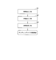
- the method for manufacturing a copper wire for bonding wire includes a hot working step S1, a wire drawing step S2, and a heat treatment step S3. Details of each step will be described below.
- a billet (ingot) having a diameter of 250 mm and a length of 700 mm made of high-purity copper having a purity of 99.9999% by mass or more is prepared. Then, the billet is heated to a temperature range of 700 ° C. to 900 ° C. and hot-extruded in a range of 99% to 99.95% of the area reduction rate to produce a strand having a wire diameter of 6 mm to 20 mm. To do.
- this hot working step S1 in order to destroy the cast structure of the billet (ingot) and make a fine and uniform hot worked structure as compared with the cast structure, in the above temperature range and area reduction rate. Hot extrusion is performed. In this embodiment, heating was performed at 800 ° C., and hot extrusion was performed under the condition of a surface reduction rate of 99.9% to produce a strand having a wire diameter of 8 mm.
- Wire drawing process S2 The wire produced in the hot working step S1 described above is drawn (cold drawing) within a range of the area reduction rate of 80% or more and 99.6% or less, and the wire diameter is 0.5 mm or more and 3 Process to 5mm or less.
- the wire drawing may be performed in one pass, but is preferably performed in a plurality of passes.
- the hot work structure (crystal grains) formed in the hot work process S1 extends in the wire drawing direction to form a fibrous metal structure.
- processing is performed from 8 mm to 1 mm in diameter (wire diameter) in 15 passes, and the area reduction rate is 98%.
- a peeling wire drawing process may be performed.
- Heat treatment step S3 The element wire drawn in the wire drawing step S2 is subjected to heat treatment within a range of 200 ° C. to 260 ° C. and 30 minutes to 300 minutes.
- the heat treatment step S3 is performed in a batch annealing furnace having a reducing atmosphere.
- a part of the metal structure made fibrous in the wire drawing step S2 is recrystallized, and a metal structure in which a fibrous metal structure and an equiaxed recrystallized structure coexist. It has become.
- the wire is heat-treated in a reducing gas atmosphere by a batch-type annealing furnace at 220 ° C. for 60 minutes.
- the copper wire for bonding wire according to the present embodiment is manufactured.
- this copper wire for bonding wires into a bonding wire it is set as a 20-micrometer bonding wire, for example by drawing at a surface reduction rate of 99.96%.
- the area ratio of the (001) plane is 15% or more and 30% or less in the cross section perpendicular to the drawing direction. The workability can be improved and the occurrence of disconnection at the time of wire drawing can be suppressed.
- the copper wire for bonding wire is made of high-purity copper having a purity of 99.9999% by mass or more, the strength of the bonding wire using the copper wire for bonding wire is sufficiently lowered, and the reliability of the bonding wire is improved. Can be improved. Moreover, since high purity copper with a purity of 99.9999% by mass or more has few inclusions, it is possible to suppress the occurrence of disconnection due to the inclusions during wire drawing.
- the manufacturing method of the copper wire for bonding wires which concerns on this embodiment is the hot working process S1 which hot-processes the ingot which consists of high purity copper, and produces a strand, and a surface area reduction rate of a strand
- a heat treatment step S3 for performing the heat treatment inside. For this reason, the copper wire for bonding wires in which the area ratio of the (001) plane is 15% or more and 30% or less in a cross section perpendicular to the wire drawing direction can be manufactured.
- the wire drawing step S2 When the wire drawing step S2 is performed within the range of the area reduction rate of 80% or more and 99.6% or less with respect to the strand produced in the hot working step S1, the crystal grains become fibrous in the drawing direction.
- An elongated metal structure is formed, and the (001) plane increases in a cross section perpendicular to the drawing direction.
- the elongation may be small (it is difficult to elongate) and may break.
- the area reduction rate in the wire drawing step S2 is preferably 89% or more and 99.5% or less, but is not limited thereto.
- the wire drawn in the wire drawing step S2 is subjected to a heat treatment within a range of 200 ° C. to 260 ° C. and 30 minutes to 300 minutes by a batch annealing furnace. I do. For this reason, the area ratio of the (001) plane in the cross section perpendicular to the wire drawing direction can be reliably controlled to 15% or more and 30% or less.
- the heating temperature in the heat treatment step S3 is preferably 210 ° C. or higher and 250 ° C. or lower, but is not limited thereto.
- the heating time is less than 30 minutes, sufficient recrystallized grains are not generated, and it becomes difficult to control the area ratio of the (001) plane to 30% or less.
- the heating time exceeds 300 minutes, recrystallization proceeds too much, and it becomes difficult to control the area ratio of the (001) plane to 15% or more.
- the heating temperature is preferably 60 minutes or more and 180 minutes or less, but is not limited thereto.
- the heat treatment conditions of the heat treatment step are set in the range of 200 ° C. to 260 ° C. and 30 minutes to 300 minutes.
- the area ratio of the (001) plane can be stably controlled within the above range by performing the heat treatment under the above heating conditions using a batch annealing furnace.
- the shape and size of the ingot which consists of high purity copper of purity 99.9999 mass% or more, and it is not limited to this embodiment.
- Comparative Example 1 a copper wire for bonding wire was manufactured without performing heat treatment after wire drawing. That is, a copper wire for bonding wire of Comparative Example 1 was manufactured in the same manner as the above-described example of the present invention except that the heat treatment after the wire drawing was not performed.
- Comparative Example 2 First, an ingot made of high-purity copper having a purity of 99.9999% or more was prepared. Using this ingot as a raw material, a strand having a diameter of 8 mm was cast. Next, a wire having a diameter of 1 mm was drawn to a diameter of 1 mm, including cold peel drawing. In this wire drawing, the area reduction rate was 98%, and the number of passes was 15. Thus, the copper wire for bonding wires of Comparative Example 2 was produced. In addition, also in the comparative example 2, the heat processing after a wire drawing process are not performed.
- EBSD measurement was performed on a cross section perpendicular to the drawing direction, and the area ratio of the (001) plane was measured.
- the EBSD measurement procedure will be described below.
- a cross section perpendicular to the wire drawing direction of the copper wire for bonding wire was mechanically polished using water-resistant abrasive paper and diamond abrasive grains, and then finish-polished using a colloidal silica solution.
- an EBSD measuring device HITACHI S4300-SEM, EDAX / TSL OIM Data Collection
- analysis software EDAX / TSL OIM Data Analysis ver.5.2
- an electron beam is irradiated to each measurement point within the measurement range of the sample surface (cross section perpendicular to the drawing direction of the copper wire for bonding wire), and the electron beam is scanned two-dimensionally on the sample surface. Then, orientation analysis by backscattered electron diffraction was performed. In addition, the measurement point interval was 1.80 ⁇ m, and EBSD measurement was performed on an area of 600 ⁇ m ⁇ 940 ⁇ m. In the cross section of the copper wire for bonding wire measured by EBSD, a crystal plane with a deviation angle of 15 ° or less (crystal plane with an angle of (001) plane within 15 °) with respect to the (001) plane. Considering it as the (001) plane, the area ratio of the (001) plane in the measurement region was evaluated.
- the manufactured copper wire for bonding wire was further drawn to a diameter of 5 ⁇ m.
- wire drawing was performed from a diameter of 1 mm (1000 ⁇ m) to 100 ⁇ m, and wire drawing was further carried out to 100 ⁇ m to 50 ⁇ m, 50 ⁇ m to 25 ⁇ m, 25 ⁇ m to 10 ⁇ m, and 10 ⁇ m to 5 ⁇ m.
- this wire drawing process was implemented so that the wire of 100 m of full length might be obtained in the step processed to 5 micrometers.
- Comparative Example 1 since wire breakage occurred frequently in the wire drawing process, the production of the wire (drawing process) was stopped halfway. The measurement results are shown in Table 1.
- Examples 1 to 5 of the present invention had good workability because the number of wire breaks was small even when wire drawing was performed from 100 ⁇ m to 5 ⁇ m.
- Examples 1 to 5 of the present invention are copper wires for bonding wires that are less likely to be broken even if they are thinned.
- Comparative Example 1 since the heat treatment was not performed after the wire was drawn to a diameter of 1 mm, the area ratio of the (001) plane was over 30%, and the number of disconnections was increased compared to the inventive example.
- Comparative Example 2 an element wire having a diameter of 8 mm is cast, and the element wire is drawn to a diameter of 1 mm. The area reduction rate of the drawing process to a diameter of 1 mm is insufficient as compared with the example of the present invention. For this reason, the area ratio of the (001) plane was less than 15%, and the number of disconnections increased compared to the inventive example.
- the workability is good and disconnection hardly occurs even if the wire is thinned, so that the bonding wire can be thinned.
Landscapes
- Chemical & Material Sciences (AREA)
- Engineering & Computer Science (AREA)
- Materials Engineering (AREA)
- Mechanical Engineering (AREA)
- Metallurgy (AREA)
- Organic Chemistry (AREA)
- Physics & Mathematics (AREA)
- Thermal Sciences (AREA)
- Crystallography & Structural Chemistry (AREA)
- Wire Bonding (AREA)
- Metal Extraction Processes (AREA)
- Non-Insulated Conductors (AREA)
Abstract
Description
本願は、2013年10月10日に、日本に出願された特願2013-213114号に基づき優先権を主張し、その内容をここに援用する。
本発明は、上記の知見に基づき完成させたものであって、その要旨は以下の通りである。
また、本発明の第二の態様に係るボンディングワイヤ用銅素線の製造方法は、純度99.9999質量%以上の高純度銅からなる鋳塊を熱間加工して素線を製出する熱間加工工程と、製出された前記素線を減面率80%以上99.6%以下の範囲内で冷間伸線加工をする伸線加工工程と、伸線加工された前記素線に対して200℃以上260℃以下、30分以上300分以下の範囲内で加熱処理を行う加熱処理工程と、を備える。
第二の態様に係るボンディング銅素線の製造方法において、前記熱間加工が、700℃以上900℃以下の温度で減面率99%以上99.95%以下まで行われる熱間押出し加工であっても良い。
また、前記加熱処理工程においてバッチ式焼鈍炉を用いて前記素線を加熱しても良い。
伸線方向と垂直な断面において、(001)面の面積率が15%未満の場合、(111)面をはじめとする他の方位が増加してしまい、強度が低下し、伸線加工時に破断が生じ易くなる。また、伸線方向と垂直な断面において(001)面の面積率が30%超の場合、伸びが低下し、伸線加工時に破断が生じ易くなる。したがって、(001)面の面積率は、上述の範囲に設定されている。
さらに、ボンディングワイヤ用銅素線が、純度99.9999質量%以上の高純度銅からなるので、このボンディングワイヤ用銅素線を用いたボンディングワイヤの強度を十分に低くし、ボンディングワイヤの信頼性を向上できる。また、純度が99.9999質量%以上の高純度銅は、介在物が少ないので、伸線加工時において介在物に起因する断線の発生を抑制できる。
本発明の第二の態様に係るボンディングワイヤ用銅素線の製造方法によれば、ボンディングワイヤ用銅素線の伸線方向と垂直な断面において(001)面の面積率を15%以上30%以下とすることができる。
そして、このボンディングワイヤ用銅素線は、伸線方向と垂直な断面において(001)面の面積率が15%以上30%以下とされている。本実施形態において、伸線方向と垂直な断面とは、ボンディングワイヤ用銅素線の中心軸を含み、この中心軸と直交する断面である。また、本実施形態では、伸線方向と垂直な断面に配向される、(001)面に対してズレ角15°以内の結晶面の合計の面積率、すなわち、伸線方向に対し15°以内に<001>方向が配向された領域の面積率を(001)面の面積率としている。
このような理由により、伸線方向と垂直な断面において(001)面の面積率は、上述の範囲に設定されている。(001)面の面積率は18%以上28%以下とすることが好ましいが、これに限定されない。
まず、純度が99.9999質量%以上の高純度銅からなる直径250mm、長さ700mmのビレット(鋳塊)を用意する。
そして、このビレットを700℃以上900℃以下の温度範囲に加熱し、減面率99%以上99.95%以下の範囲で熱間押出し加工し、線径6mm以上20mm以下の素線を製出する。この熱間加工工程S1においては、ビレット(鋳塊)が有する鋳造組織を破壊し、鋳造組織に比較して微細で均一な熱間加工組織にするために、上述の温度範囲及び減面率で熱間押出し加工を行っている。
本実施形態においては、800℃に加熱し、減面率99.9%の条件で熱間押出し加工を行い、線径8mmの素線を製出した。
上述の熱間加工工程S1において製出された素線を、減面率80%以上99.6%以下の範囲内で伸線加工(冷間伸線加工)し、線径0.5mm以上3.5mm以下に加工する。ここで、伸線加工は、1パスで行われても良いが、複数パスに分けて行われることが好ましい。この伸線加工工程S2においては、熱間加工工程S1で形成された熱間加工組織(結晶粒)が伸線加工方向に伸長し、繊維状の金属組織となる。
本実施形態においては、15パスで直径(線径)8mmから1mmまで加工を行っており、減面率は98%とされている。
なお、伸線加工工程S2においては、皮剥ぎ伸線加工が行われても良い。
上述の伸線加工工程S2において伸線された素線に対して200℃以上260℃以下、30分以上300分以下の範囲内で加熱処理を行う。ここで、加熱処理工程S3は、還元雰囲気とされたバッチ式焼鈍炉で行われる。この加熱処理工程S3においては、伸線加工工程S2で繊維状とされた金属組織のうちの一部が再結晶し、繊維状の金属組織と等軸の再結晶組織とが混在した金属組織となっている。
本実施形態においては、バッチ式焼鈍炉によって、220℃で60分の条件で、還元ガス雰囲気中で素線の加熱処理が行われている。
なお、このボンディングワイヤ用銅素線をボンディングワイヤに加工する場合、例えば減面率99.96%で伸線加工することにより、20μmのボンディングワイヤとされる。
以上の理由により、加熱処理工程の熱処理条件は、200℃以上260℃以下、30分以上300分以下の範囲内とされている。
(本発明例1~5)
まず、純度99.9999質量%以上の高純度銅からなる直径250mm、長さ700mmのビレットを用意した。このビレットを800℃に加熱し、熱間押出し加工を行い、直径8mmの素線を製出した。
次に、直径8mmの素線に対して、冷間皮剥ぎ伸線を含め、直径1mmまで伸線加工を行った。なお、この伸線加工は、減面率98%とし、パス回数は15回とした。
次いで、伸線加工された素線をバッチ式焼鈍炉に装入して、表1に示す加熱温度、加熱時間で加熱処理を行った。なお、バッチ式焼鈍炉の雰囲気は、還元雰囲気とした。
以上のようにして、本発明例1~5のボンディングワイヤ用銅素線を製造した。
比較例1では、伸線加工後の加熱処理を行わずにボンディングワイヤ用銅素線を製造した。すなわち、伸線加工後の加熱処理を行わないこと以外は、上述した本発明例と同様にして、比較例1のボンディングワイヤ用銅素線を製造した。
まず、純度99.9999%以上の高純度銅からなる鋳塊を用意した。この鋳塊を原料として直径8mmの素線を鋳造した。
次に、直径8mmの素線に対して、冷間皮剥ぎ伸線を含め、直径1mmまで伸線加工を行った。なお、この伸線加工は、減面率98%とし、パス回数は15回とした。
このようにして、比較例2のボンディングワイヤ用銅素線を製造した。なお、比較例2においても、伸線加工後の加熱処理を行っていない。
EBSD測定の手順について以下に説明する。まず、ボンディングワイヤ用銅素線の伸線方向に垂直な断面を耐水研磨紙、及びダイヤモンド砥粒を用いて機械研磨した後、コロイダルシリカ溶液を用いて仕上げ研磨した。そして、EBSD測定装置(HITACHI社製 S4300-SEM、EDAX/TSL社製 OIM Data Collection)と、解析ソフト(EDAX/TSL社製 OIM Data Analysis ver.5.2)によって、ボンディングワイヤ用銅素線の伸線方向に垂直な断面の結晶方位を測定した。具体的には、試料表面(ボンディングワイヤ用銅素線の伸線方向に垂直な断面)の測定範囲内の個々の測定点に電子線を照射し、電子線を試料表面に2次元で走査させ、後方散乱電子線回折による方位解析を行った。なお、測定点間隔を1.80μmとし、600μm×940μmの領域についてEBSD測定を行った。
なお、EBSD測定されるボンディングワイヤ用銅素線の断面において、(001)面に対してズレ角15°以内の結晶面((001)面との為す角度が15°以内にある結晶面)を(001)面とみなして、測定領域における(001)面の面積率を評価した。
なお、比較例1については、伸線加工において、断線が多発したため、途中でワイヤの製造(伸線加工)を中止した。
上記の測定結果を表1に示す。

また、比較例2は、直径8mmの素線を鋳造し、この素線を直径1mmまで伸線加工しており、直径1mmまでの伸線加工の減面率が本発明例と比較して不足しているために、(001)面の面積率が15%未満となり、断線回数が本発明例と比較して多くなった。
S2 伸線加工工程
S3 加熱処理工程
Claims (4)
- ボンディングワイヤを形成するためのボンディングワイヤ用銅素線であって、
純度が99.9999質量%以上の高純度銅からなり、
線径が0.5mm以上3.5mm以下であり、
伸線方向と垂直な断面において(001)面の面積率が15%以上30%以下であることを特徴とするボンディングワイヤ用銅素線。 - 純度99.9999質量%以上の高純度銅からなる鋳塊を熱間加工して素線を製出する熱間加工工程と、
製出された前記素線を減面率80%以上99.6%以下の範囲内で冷間伸線加工をする伸線加工工程と、
伸線加工された前記素線に対して200℃以上260℃以下、30分以上300分以下の範囲内で加熱処理を行う加熱処理工程と、
を備えるボンディングワイヤ用銅素線の製造方法。 - 前記熱間加工が、700℃以上900℃以下の温度で減面率99%以上99.95%以下まで行われる熱間押出し加工である、請求項2に記載のボンディングワイヤ用銅素線の製造方法。
- 前記加熱処理工程においてバッチ式焼鈍炉を用いて前記素線を加熱する、請求項2または3に記載のボンディングワイヤ用銅素線の製造方法。
Priority Applications (3)
| Application Number | Priority Date | Filing Date | Title |
|---|---|---|---|
| CN201480004297.7A CN104904000B (zh) | 2013-10-10 | 2014-09-30 | 接合线用铜线材及接合线用铜线材的制造方法 |
| SG11201602116YA SG11201602116YA (en) | 2013-10-10 | 2014-09-30 | Copper wire for bonding wire and method of producing copper wire for bonding wire |
| PH12016500617A PH12016500617A1 (en) | 2013-10-10 | 2016-04-05 | Copper wire for bonding wire and method of producing copper wire for bonding wire |
Applications Claiming Priority (2)
| Application Number | Priority Date | Filing Date | Title |
|---|---|---|---|
| JP2013213114A JP5747970B2 (ja) | 2013-10-10 | 2013-10-10 | ボンディングワイヤ用銅素線 |
| JP2013-213114 | 2013-10-10 |
Publications (1)
| Publication Number | Publication Date |
|---|---|
| WO2015053128A1 true WO2015053128A1 (ja) | 2015-04-16 |
Family
ID=52812946
Family Applications (1)
| Application Number | Title | Priority Date | Filing Date |
|---|---|---|---|
| PCT/JP2014/075999 Ceased WO2015053128A1 (ja) | 2013-10-10 | 2014-09-30 | ボンディングワイヤ用銅素線、及びボンディングワイヤ用銅素線の製造方法 |
Country Status (8)
| Country | Link |
|---|---|
| JP (1) | JP5747970B2 (ja) |
| KR (1) | KR101558138B1 (ja) |
| CN (1) | CN104904000B (ja) |
| MY (1) | MY177767A (ja) |
| PH (1) | PH12016500617A1 (ja) |
| SG (1) | SG11201602116YA (ja) |
| TW (1) | TWI540212B (ja) |
| WO (1) | WO2015053128A1 (ja) |
Cited By (2)
| Publication number | Priority date | Publication date | Assignee | Title |
|---|---|---|---|---|
| WO2019031498A1 (ja) * | 2017-08-09 | 2019-02-14 | 日鉄ケミカル&マテリアル株式会社 | 半導体装置用Cu合金ボンディングワイヤ |
| WO2019031497A1 (ja) * | 2017-08-09 | 2019-02-14 | 日鉄ケミカル&マテリアル株式会社 | 半導体装置用Cu合金ボンディングワイヤ |
Families Citing this family (4)
| Publication number | Priority date | Publication date | Assignee | Title |
|---|---|---|---|---|
| KR102810270B1 (ko) * | 2022-03-08 | 2025-05-26 | 엘티메탈 주식회사 | 본딩 와이어의 제조방법 및 이로부터 제조된 본딩 와이어 |
| KR102812812B1 (ko) * | 2022-03-08 | 2025-05-27 | 엘티메탈 주식회사 | 본딩 와이어의 제조방법 및 이로부터 제조된 본딩 와이어 |
| KR102812817B1 (ko) * | 2022-12-14 | 2025-05-27 | 엘티메탈 주식회사 | 본딩 와이어의 제조방법 및 이로부터 제조된 본딩 와이어 |
| KR102812809B1 (ko) * | 2022-12-14 | 2025-05-27 | 엘티메탈 주식회사 | 본딩 와이어의 제조방법 및 이로부터 제조된 본딩 와이어 |
Citations (2)
| Publication number | Priority date | Publication date | Assignee | Title |
|---|---|---|---|---|
| JPH0786325A (ja) * | 1993-09-14 | 1995-03-31 | Hitachi Cable Ltd | 電子機器用銅線 |
| JP2013057121A (ja) * | 2011-08-17 | 2013-03-28 | Hitachi Cable Ltd | 軟質希薄銅合金材料の製造方法 |
Family Cites Families (2)
| Publication number | Priority date | Publication date | Assignee | Title |
|---|---|---|---|---|
| KR101006035B1 (ko) * | 2005-06-15 | 2011-01-06 | 제이엑스 닛코 닛세키 킨조쿠 가부시키가이샤 | 초고순도 구리 및 그 제조 방법 그리고 초고순도 구리로이루어지는 본딩 와이어 |
| JP4885117B2 (ja) * | 2007-12-03 | 2012-02-29 | 新日鉄マテリアルズ株式会社 | 半導体装置用ボンディングワイヤ |
-
2013
- 2013-10-10 JP JP2013213114A patent/JP5747970B2/ja active Active
-
2014
- 2014-09-30 WO PCT/JP2014/075999 patent/WO2015053128A1/ja not_active Ceased
- 2014-09-30 MY MYPI2016701080A patent/MY177767A/en unknown
- 2014-09-30 CN CN201480004297.7A patent/CN104904000B/zh active Active
- 2014-09-30 KR KR1020157018027A patent/KR101558138B1/ko active Active
- 2014-09-30 SG SG11201602116YA patent/SG11201602116YA/en unknown
- 2014-10-03 TW TW103134559A patent/TWI540212B/zh active
-
2016
- 2016-04-05 PH PH12016500617A patent/PH12016500617A1/en unknown
Patent Citations (2)
| Publication number | Priority date | Publication date | Assignee | Title |
|---|---|---|---|---|
| JPH0786325A (ja) * | 1993-09-14 | 1995-03-31 | Hitachi Cable Ltd | 電子機器用銅線 |
| JP2013057121A (ja) * | 2011-08-17 | 2013-03-28 | Hitachi Cable Ltd | 軟質希薄銅合金材料の製造方法 |
Cited By (9)
| Publication number | Priority date | Publication date | Assignee | Title |
|---|---|---|---|---|
| WO2019031498A1 (ja) * | 2017-08-09 | 2019-02-14 | 日鉄ケミカル&マテリアル株式会社 | 半導体装置用Cu合金ボンディングワイヤ |
| WO2019031497A1 (ja) * | 2017-08-09 | 2019-02-14 | 日鉄ケミカル&マテリアル株式会社 | 半導体装置用Cu合金ボンディングワイヤ |
| JPWO2019031497A1 (ja) * | 2017-08-09 | 2019-11-07 | 日鉄ケミカル&マテリアル株式会社 | 半導体装置用Cu合金ボンディングワイヤ |
| JPWO2019031498A1 (ja) * | 2017-08-09 | 2020-01-09 | 日鉄ケミカル&マテリアル株式会社 | 半導体装置用Cu合金ボンディングワイヤ |
| CN110998814A (zh) * | 2017-08-09 | 2020-04-10 | 日铁化学材料株式会社 | 半导体装置用Cu合金接合线 |
| TWI692822B (zh) * | 2017-08-09 | 2020-05-01 | 日商日鐵化學材料股份有限公司 | 半導體裝置用銅合金接合導線 |
| US10790259B2 (en) | 2017-08-09 | 2020-09-29 | Nippon Steel Chemical & Material Co., Ltd. | Cu alloy bonding wire for semiconductor device |
| CN110998814B (zh) * | 2017-08-09 | 2021-04-23 | 日铁化学材料株式会社 | 半导体装置用Cu合金接合线 |
| US10991672B2 (en) | 2017-08-09 | 2021-04-27 | Nippon Steel Chemical & Material Co., Ltd. | Cu alloy bonding wire for semiconductor device |
Also Published As
| Publication number | Publication date |
|---|---|
| JP2015076559A (ja) | 2015-04-20 |
| KR101558138B1 (ko) | 2015-10-06 |
| CN104904000B (zh) | 2019-05-17 |
| PH12016500617B1 (en) | 2016-06-13 |
| TWI540212B (zh) | 2016-07-01 |
| KR20150085126A (ko) | 2015-07-22 |
| SG11201602116YA (en) | 2016-05-30 |
| JP5747970B2 (ja) | 2015-07-15 |
| CN104904000A (zh) | 2015-09-09 |
| PH12016500617A1 (en) | 2016-06-13 |
| TW201522673A (zh) | 2015-06-16 |
| MY177767A (en) | 2020-09-23 |
Similar Documents
| Publication | Publication Date | Title |
|---|---|---|
| JP5747970B2 (ja) | ボンディングワイヤ用銅素線 | |
| CN105518165B (zh) | 铜合金线材及其制造方法 | |
| KR101704839B1 (ko) | 반도체용 구리 합금 본딩 와이어 | |
| JP5344070B2 (ja) | ボンディングワイヤ用銅素線及びボンディングワイヤ用銅素線の製造方法 | |
| CN106164306B (zh) | 铜合金线材及其制造方法 | |
| JP5772338B2 (ja) | 軟質希薄銅合金線、軟質希薄銅合金板及び軟質希薄銅合金撚線 | |
| CN108463568B (zh) | 铜合金线材及铜合金线材的制造方法 | |
| WO2021177469A1 (ja) | 純銅板 | |
| TW201247908A (en) | Cu-co-si-based copper alloy strip for electron material, and method for manufacturing same | |
| CN102482732A (zh) | 铜合金线材及其制造方法 | |
| KR20140049591A (ko) | 구리 합금 선재 및 그 제조 방법 | |
| JP2015161009A (ja) | 高強度銅合金薄板材およびその製造方法 | |
| JP2013194246A (ja) | 残留応力の少ないリードフレーム用Cu−Cr−Sn系銅合金板 | |
| JP2013057121A (ja) | 軟質希薄銅合金材料の製造方法 | |
| JP6175932B2 (ja) | 引抜銅線、引抜銅線の製造方法及びケーブル | |
| JP2017002368A (ja) | 銅合金材 | |
| CN102637485B (zh) | 铝合金线及其制备方法 | |
| JP5609564B2 (ja) | 溶融はんだめっき線の製造方法 | |
| CN109003743A (zh) | 一种连续铜合金极细导体的制作方法 | |
| CN117836450A (zh) | 钨线和使用该钨线的加工方法以及电解线 | |
| JP5757547B1 (ja) | Rh基合金からなるプローブピン及びその製造方法 | |
| JP4019892B2 (ja) | ワイヤ放電加工用電極線の製造方法及びその製造方法を用いて製造したワイヤ放電加工用電極線 | |
| JP2016160470A (ja) | 銅合金材、リードフレームおよびコネクタ | |
| JP5741849B2 (ja) | 太陽電池インターコネクタ用導体及び太陽電池用インターコネクタ |
Legal Events
| Date | Code | Title | Description |
|---|---|---|---|
| 121 | Ep: the epo has been informed by wipo that ep was designated in this application |
Ref document number: 14851820 Country of ref document: EP Kind code of ref document: A1 |
|
| ENP | Entry into the national phase |
Ref document number: 20157018027 Country of ref document: KR Kind code of ref document: A |
|
| WWE | Wipo information: entry into national phase |
Ref document number: 12016500617 Country of ref document: PH |
|
| NENP | Non-entry into the national phase |
Ref country code: DE |
|
| 122 | Ep: pct application non-entry in european phase |
Ref document number: 14851820 Country of ref document: EP Kind code of ref document: A1 |