WO2015045915A1 - 固体撮像素子及びその駆動方法、並びに電子機器 - Google Patents
固体撮像素子及びその駆動方法、並びに電子機器 Download PDFInfo
- Publication number
- WO2015045915A1 WO2015045915A1 PCT/JP2014/074245 JP2014074245W WO2015045915A1 WO 2015045915 A1 WO2015045915 A1 WO 2015045915A1 JP 2014074245 W JP2014074245 W JP 2014074245W WO 2015045915 A1 WO2015045915 A1 WO 2015045915A1
- Authority
- WO
- WIPO (PCT)
- Prior art keywords
- photoelectric conversion
- conversion unit
- region
- pixel
- phase difference
- Prior art date
Links
- 238000003384 imaging method Methods 0.000 title claims abstract description 66
- 238000000034 method Methods 0.000 title claims abstract description 31
- 239000007787 solid Substances 0.000 title abstract 2
- 238000006243 chemical reaction Methods 0.000 claims abstract description 147
- 238000001514 detection method Methods 0.000 claims abstract description 20
- 238000009825 accumulation Methods 0.000 claims abstract description 18
- 239000011159 matrix material Substances 0.000 claims abstract description 14
- 238000012546 transfer Methods 0.000 claims description 72
- 239000012535 impurity Substances 0.000 claims description 31
- 238000012937 correction Methods 0.000 claims description 18
- 210000001747 pupil Anatomy 0.000 claims description 18
- 238000009792 diffusion process Methods 0.000 claims description 10
- 239000002184 metal Substances 0.000 claims description 5
- 238000000926 separation method Methods 0.000 claims description 4
- 238000005516 engineering process Methods 0.000 abstract description 24
- 238000012545 processing Methods 0.000 description 30
- 230000000875 corresponding effect Effects 0.000 description 14
- 230000002093 peripheral effect Effects 0.000 description 14
- 230000006870 function Effects 0.000 description 9
- 238000002955 isolation Methods 0.000 description 8
- 239000000758 substrate Substances 0.000 description 7
- 230000003321 amplification Effects 0.000 description 6
- 238000003199 nucleic acid amplification method Methods 0.000 description 6
- 239000004065 semiconductor Substances 0.000 description 6
- 238000010586 diagram Methods 0.000 description 5
- 230000003287 optical effect Effects 0.000 description 5
- 238000013500 data storage Methods 0.000 description 4
- 230000007423 decrease Effects 0.000 description 3
- 238000004364 calculation method Methods 0.000 description 1
- 230000000295 complement effect Effects 0.000 description 1
- 230000002596 correlated effect Effects 0.000 description 1
- 238000005401 electroluminescence Methods 0.000 description 1
- 239000004973 liquid crystal related substance Substances 0.000 description 1
- 229910044991 metal oxide Inorganic materials 0.000 description 1
- 150000004706 metal oxides Chemical class 0.000 description 1
- 238000012986 modification Methods 0.000 description 1
- 230000004048 modification Effects 0.000 description 1
- 239000002245 particle Substances 0.000 description 1
- 230000011514 reflex Effects 0.000 description 1
- 238000005070 sampling Methods 0.000 description 1
- 230000001629 suppression Effects 0.000 description 1
Images


Classifications
-
- H—ELECTRICITY
- H01—ELECTRIC ELEMENTS
- H01L—SEMICONDUCTOR DEVICES NOT COVERED BY CLASS H10
- H01L27/00—Devices consisting of a plurality of semiconductor or other solid-state components formed in or on a common substrate
- H01L27/14—Devices consisting of a plurality of semiconductor or other solid-state components formed in or on a common substrate including semiconductor components sensitive to infrared radiation, light, electromagnetic radiation of shorter wavelength or corpuscular radiation and specially adapted either for the conversion of the energy of such radiation into electrical energy or for the control of electrical energy by such radiation
- H01L27/144—Devices controlled by radiation
- H01L27/146—Imager structures
-
- H—ELECTRICITY
- H04—ELECTRIC COMMUNICATION TECHNIQUE
- H04N—PICTORIAL COMMUNICATION, e.g. TELEVISION
- H04N25/00—Circuitry of solid-state image sensors [SSIS]; Control thereof
- H04N25/70—SSIS architectures; Circuits associated therewith
- H04N25/703—SSIS architectures incorporating pixels for producing signals other than image signals
- H04N25/704—Pixels specially adapted for focusing, e.g. phase difference pixel sets
-
- H—ELECTRICITY
- H01—ELECTRIC ELEMENTS
- H01L—SEMICONDUCTOR DEVICES NOT COVERED BY CLASS H10
- H01L27/00—Devices consisting of a plurality of semiconductor or other solid-state components formed in or on a common substrate
- H01L27/14—Devices consisting of a plurality of semiconductor or other solid-state components formed in or on a common substrate including semiconductor components sensitive to infrared radiation, light, electromagnetic radiation of shorter wavelength or corpuscular radiation and specially adapted either for the conversion of the energy of such radiation into electrical energy or for the control of electrical energy by such radiation
- H01L27/144—Devices controlled by radiation
- H01L27/146—Imager structures
- H01L27/14601—Structural or functional details thereof
- H01L27/14603—Special geometry or disposition of pixel-elements, address-lines or gate-electrodes
- H01L27/14605—Structural or functional details relating to the position of the pixel elements, e.g. smaller pixel elements in the center of the imager compared to pixel elements at the periphery
-
- H—ELECTRICITY
- H01—ELECTRIC ELEMENTS
- H01L—SEMICONDUCTOR DEVICES NOT COVERED BY CLASS H10
- H01L27/00—Devices consisting of a plurality of semiconductor or other solid-state components formed in or on a common substrate
- H01L27/14—Devices consisting of a plurality of semiconductor or other solid-state components formed in or on a common substrate including semiconductor components sensitive to infrared radiation, light, electromagnetic radiation of shorter wavelength or corpuscular radiation and specially adapted either for the conversion of the energy of such radiation into electrical energy or for the control of electrical energy by such radiation
- H01L27/144—Devices controlled by radiation
- H01L27/146—Imager structures
- H01L27/14601—Structural or functional details thereof
- H01L27/14609—Pixel-elements with integrated switching, control, storage or amplification elements
- H01L27/1461—Pixel-elements with integrated switching, control, storage or amplification elements characterised by the photosensitive area
-
- H—ELECTRICITY
- H01—ELECTRIC ELEMENTS
- H01L—SEMICONDUCTOR DEVICES NOT COVERED BY CLASS H10
- H01L27/00—Devices consisting of a plurality of semiconductor or other solid-state components formed in or on a common substrate
- H01L27/14—Devices consisting of a plurality of semiconductor or other solid-state components formed in or on a common substrate including semiconductor components sensitive to infrared radiation, light, electromagnetic radiation of shorter wavelength or corpuscular radiation and specially adapted either for the conversion of the energy of such radiation into electrical energy or for the control of electrical energy by such radiation
- H01L27/144—Devices controlled by radiation
- H01L27/146—Imager structures
- H01L27/14643—Photodiode arrays; MOS imagers
- H01L27/14645—Colour imagers
-
- H—ELECTRICITY
- H04—ELECTRIC COMMUNICATION TECHNIQUE
- H04N—PICTORIAL COMMUNICATION, e.g. TELEVISION
- H04N23/00—Cameras or camera modules comprising electronic image sensors; Control thereof
- H04N23/60—Control of cameras or camera modules
- H04N23/67—Focus control based on electronic image sensor signals
- H04N23/672—Focus control based on electronic image sensor signals based on the phase difference signals
-
- H—ELECTRICITY
- H04—ELECTRIC COMMUNICATION TECHNIQUE
- H04N—PICTORIAL COMMUNICATION, e.g. TELEVISION
- H04N25/00—Circuitry of solid-state image sensors [SSIS]; Control thereof
- H04N25/60—Noise processing, e.g. detecting, correcting, reducing or removing noise
-
- H—ELECTRICITY
- H04—ELECTRIC COMMUNICATION TECHNIQUE
- H04N—PICTORIAL COMMUNICATION, e.g. TELEVISION
- H04N25/00—Circuitry of solid-state image sensors [SSIS]; Control thereof
- H04N25/60—Noise processing, e.g. detecting, correcting, reducing or removing noise
- H04N25/616—Noise processing, e.g. detecting, correcting, reducing or removing noise involving a correlated sampling function, e.g. correlated double sampling [CDS] or triple sampling
-
- H—ELECTRICITY
- H04—ELECTRIC COMMUNICATION TECHNIQUE
- H04N—PICTORIAL COMMUNICATION, e.g. TELEVISION
- H04N25/00—Circuitry of solid-state image sensors [SSIS]; Control thereof
- H04N25/60—Noise processing, e.g. detecting, correcting, reducing or removing noise
- H04N25/67—Noise processing, e.g. detecting, correcting, reducing or removing noise applied to fixed-pattern noise, e.g. non-uniformity of response
- H04N25/671—Noise processing, e.g. detecting, correcting, reducing or removing noise applied to fixed-pattern noise, e.g. non-uniformity of response for non-uniformity detection or correction
-
- H—ELECTRICITY
- H04—ELECTRIC COMMUNICATION TECHNIQUE
- H04N—PICTORIAL COMMUNICATION, e.g. TELEVISION
- H04N25/00—Circuitry of solid-state image sensors [SSIS]; Control thereof
- H04N25/70—SSIS architectures; Circuits associated therewith
- H04N25/76—Addressed sensors, e.g. MOS or CMOS sensors
-
- H—ELECTRICITY
- H04—ELECTRIC COMMUNICATION TECHNIQUE
- H04N—PICTORIAL COMMUNICATION, e.g. TELEVISION
- H04N25/00—Circuitry of solid-state image sensors [SSIS]; Control thereof
- H04N25/10—Circuitry of solid-state image sensors [SSIS]; Control thereof for transforming different wavelengths into image signals
- H04N25/11—Arrangement of colour filter arrays [CFA]; Filter mosaics
- H04N25/13—Arrangement of colour filter arrays [CFA]; Filter mosaics characterised by the spectral characteristics of the filter elements
- H04N25/134—Arrangement of colour filter arrays [CFA]; Filter mosaics characterised by the spectral characteristics of the filter elements based on three different wavelength filter elements
Definitions
- the present technology relates to a solid-state imaging device, a driving method thereof, and an electronic device, and in particular, a solid-state imaging device capable of making the characteristics of a phase difference pixel constant regardless of a chip position, a driving method thereof, and an electronic device Regarding equipment.
- CMOS Complementary Metal Oxide Semiconductor
- AF Autofocus
- a digital single-lens reflex camera has an additional AF module, which increases the housing size and mounting cost.
- some mirrorless interchangeable-lens cameras and compact digital still cameras have an AF function that does not incorporate an AF module and uses contrast AF.
- phase difference pixels A and B are paired to realize the AF function.
- the phase difference pixels A and B are made the same size as the normal pixels for imaging, for example, by changing the metal shading.
- Patent Document 1 discloses a technique for increasing AF accuracy by mounting phase difference pixels A and B in one pixel and increasing the number of AF pixels.
- Patent Document 2 discloses a technique related to a back-illuminated phase difference pixel.
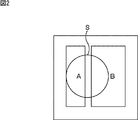
- Patent Document 1 discloses a PD division type image plane phase difference AF. This is a method in which the phase difference pixels A and B are mounted in one pixel, and the condensing spot S is set at the boundary between the phase difference pixel A and the phase difference pixel B.
- the focused spot position changes depending on the F value of the interchangeable lens. Even if the lens is not exchanged, if the zoom is performed with a wide angle or telephoto, the F value changes, and the condensing spot position changes accordingly.
- the condensing spot S since the condensing spot S does not change in any lens at the center of the angle of view (the center of the chip), the phase difference pixel A and the phase difference pixel B have the same size. Then, the condensing spot S can be set at the boundary between the phase difference pixel A and the phase difference pixel B.
- FIG. 1 shows an example in which a condensing spot S is set at the center of the pixel.
- a condensing spot S can be set at the center of a pixel in a certain lens, but if a lens having a different F value is used, the light is condensed. It is possible that the spot S deviates from the center of the pixel. In this case, in order to set the condensing spot S at the boundary between the phase difference pixel A and the phase difference pixel B, it is necessary to change the sizes of the light receiving surfaces of the phase difference pixel A and the phase difference pixel B.
- FIG. 2 shows an example in which the size of the phase difference pixel A is smaller than the size of the phase difference pixel B.
- Patent Document 2 discloses a technique related to a back-illuminated phase difference pixel, but does not employ a PD division method.
- the present technology has been made in view of such a situation, and makes it possible to make the characteristics of the phase difference pixel constant regardless of the chip position such as the central portion of the angle of view or the peripheral portion of the angle of view. is there.
- a solid-state imaging device includes a photoelectric conversion unit that receives and photoelectrically converts incident light, and includes a first pixel from which a color component signal is obtained, and a light receiving surface having a size corresponding to an image height.
- a pixel array unit having a pair of first photoelectric conversion units and a second photoelectric conversion unit, wherein second pixels from which phase difference detection signals are obtained are arranged in a matrix, and the pair of first photoelectric conversion units
- the photoelectric conversion unit and the second photoelectric conversion unit each include a first region that is a main part of charge accumulation and a second region that performs photoelectric conversion and contributes to charge transfer to the main unit. Yes.
- the second region on the light incident side has a size corresponding to pupil correction, and the second region on the opposite side of the light incident side.
- One area has the same size.
- the impurity concentration in the first region is higher than the impurity concentration in the second region.
- the second area is larger than the first area.
- the impurity concentration in the region in the vicinity of the first transfer transistor and the region in the vicinity of the second transfer transistor are the impurity concentrations in other regions. Higher than.
- the first transfer transistor is disposed in the vicinity of the position closest to the center of the light receiving surface of the first photoelectric conversion unit, and the second transfer transistor is the center of the light receiving surface of the second photoelectric conversion unit. Near the nearest position.
- a first floating diffusion region that holds the charge transferred from the first photoelectric conversion unit by the first transfer transistor as a signal; and the second transfer transistor from the second photoelectric conversion unit. And a second floating diffusion region for holding the transferred charge as a signal.
- Exposure and transfer in the first photoelectric conversion unit and the second photoelectric conversion unit are performed simultaneously.
- the separation unit of the pair of the first photoelectric conversion unit and the second photoelectric conversion unit is continuously changed.
- the pair of the first photoelectric conversion unit and the second photoelectric conversion unit are separated by a metal, an oxide film, or an impurity.
- the pixel array unit includes a photoelectric conversion unit that receives and photoelectrically converts incident light, and the light receiving surface has an image height.
- a pair of first photoelectric conversion units and second photoelectric conversion units each having a size corresponding to the second pixel from which the phase difference detection signal is obtained are arranged in a matrix, and the pair of first photoelectric conversion units
- the photoelectric conversion unit and the second photoelectric conversion unit are provided with a first region that is a main part of charge accumulation and a second region that performs photoelectric conversion and contributes to charge transfer to the main part.
- a driving method includes a photoelectric conversion unit that receives and photoelectrically converts incident light, a pair of first pixels from which a color component signal is obtained, and a light receiving surface having a size corresponding to the image height.
- a pixel array unit having a first photoelectric conversion unit and a second photoelectric conversion unit, in which second pixels from which a phase difference detection signal is obtained are arranged in a matrix, and a pair of the first photoelectric conversion units
- the conversion unit and the second photoelectric conversion unit each have a first region that is a main part of charge accumulation and a second region that performs photoelectric conversion and contributes to charge transfer to the main part.
- the pixel driving unit separately drives the pair of the first photoelectric conversion unit and the second photoelectric conversion unit, so that the first photoelectric conversion unit and the second photoelectric conversion unit are driven. And a step of simultaneously performing exposure and transfer in the conversion unit.
- the pair of the first photoelectric conversion unit and the second photoelectric conversion unit whose light-receiving surface has a size corresponding to the image height are separately driven, and the first photoelectric conversion unit and Exposure and transfer in the second photoelectric conversion unit are performed simultaneously.
- An electronic device includes a photoelectric conversion unit that receives and photoelectrically converts incident light, and a pair of first pixels from which a color component signal is obtained and a light receiving surface having a size corresponding to the image height.
- a pixel array unit having a first photoelectric conversion unit and a second photoelectric conversion unit, in which second pixels from which a phase difference detection signal is obtained are arranged in a matrix, and a pair of the first photoelectric conversion units
- the conversion unit and the second photoelectric conversion unit each have a first region that is a main part of charge accumulation and a second region that performs photoelectric conversion and contributes to charge transfer to the main part.
- a solid-state imaging device is mounted, and a control unit that controls an image plane phase difference AF (Autofocus) using the phase difference detection signal output from the solid-state imaging device is provided.
- the image plane phase difference AF is controlled using the phase difference detection signal output from the solid-state imaging device.
- the characteristics of the phase difference pixel can be made constant regardless of the chip position.
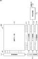
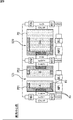
- FIG. 3 is a block diagram showing a configuration of an embodiment of a solid-state imaging device to which the present technology is applied.
- the CMOS image sensor 100 is an example of a solid-state image sensor. As shown in FIG. 3, the CMOS image sensor 100 includes a pixel array unit 111 and a peripheral circuit unit.
- the peripheral circuit unit includes a vertical driving unit 112, a column processing unit 113, a horizontal driving unit 114, and a system control unit 115.
- the CMOS image sensor 100 further includes a signal processing unit 118 and a data storage unit 119.
- the signal processing unit 118 and the data storage unit 119 may be mounted on the same semiconductor substrate as the CMOS image sensor 100, or an external signal processing unit provided on a semiconductor substrate different from the CMOS image sensor 100, for example, a DSP (Digital Signal Processor) or software processing is also acceptable.
- DSP Digital Signal Processor
- unit pixels having a photoelectric conversion unit (hereinafter sometimes simply referred to as “pixels”) are two-dimensionally arranged in a matrix. The specific configuration of the unit pixel will be described later. Further, in the pixel array unit 111, pixel drive lines 116 are formed along the horizontal direction of the figure for each row with respect to the matrix-like pixel arrangement, and vertical signal lines 117 are formed along the vertical direction of the figure for each column. Has been. One end of the pixel drive line 116 is connected to an output end corresponding to each row of the vertical drive unit 112.
- the vertical drive unit 112 is configured by a shift register, an address decoder, or the like, and is a pixel drive unit that drives each pixel of the pixel array unit 111 at the same time or in units of rows.
- a signal output from each unit pixel of the pixel row selectively scanned by the vertical driving unit 112 is supplied to the column processing unit 113 through each vertical signal line 117.
- the column processing unit 113 performs predetermined signal processing on signals output from the unit pixels of the selected row through the vertical signal line 117 for each pixel column of the pixel array unit 111, and outputs the pixel signal after the signal processing. Hold temporarily.
- the column processing unit 113 performs at least noise removal processing such as CDS (Correlated Double Double Double Sampling) processing as signal processing.
- the CDS processing by the column processing unit 113 removes pixel-specific fixed pattern noise such as reset noise and threshold variation of the amplification transistor.
- the column processing unit 113 may have an A / D (Analog / Digital) conversion function, for example, and output a signal level as a digital signal.
- the horizontal driving unit 114 includes a shift register, an address decoder, and the like, and sequentially selects unit circuits corresponding to the pixel columns of the column processing unit 113. By the selective scanning by the horizontal driving unit 114, the pixel signals subjected to signal processing by the column processing unit 113 are sequentially output.
- the system control unit 115 includes a timing generator that generates various timing signals, and based on the various timing signals generated by the timing generator, the vertical driving unit 112, the column processing unit 113, the horizontal driving unit 114, And drive control of the data storage part 119 etc. is performed.
- the signal processing unit 118 has at least an addition processing function, and performs various signal processing such as addition processing on the pixel signal output from the column processing unit 113.
- the data storage unit 119 temporarily stores data necessary for the signal processing in the signal processing unit 118.
- the CMOS image sensor 100 is a back surface that reads from the front surface side of the semiconductor substrate a signal corresponding to the charge generated in the photoelectric conversion portion by light incident on the photoelectric conversion portion in the semiconductor substrate from the back surface side of the semiconductor substrate. This is an irradiation type image sensor.
- the unit pixel includes a normal pixel 120 for outputting a color component signal for forming an image signal indicating an image of a subject as a pixel signal, and a phase difference detection signal used for the image plane phase difference AF as a pixel signal. As a result, a phase difference pixel 121 is output.
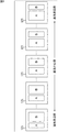
- FIG. 4 illustrates the phase difference pixels 121 arranged in a row among the unit pixels arranged in the pixel array unit 111.
- the phase difference pixel 121 has a light receiving surface of the same size in the central portion of the angle of view on the axis (the center portion of the chip), but the peripheral portion of the angle of view that is off-axis.
- the size of the light receiving surface varies depending on the image height.
- the phase difference pixel 121 arranged in the left direction in the drawing has a smaller light receiving surface size of the phase difference pixel 121 ⁇ / b> A, while the phase difference pixel arranged in the right direction in the drawing.
- the size of the light receiving surface of the phase difference pixel 121B becomes smaller.
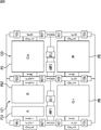
- FIG. 5 and 6 are plan views showing the configuration of the unit pixel.
- FIG. 5 shows the configuration of unit pixels in the center of the angle of view
- FIG. 6 shows the configuration of unit pixels in the periphery of the angle of view.
- the normal pixel 120 includes a photodiode (PD) as a photoelectric conversion unit and a plurality of pixel transistors.
- the photodiode (PD) has a region for receiving incident light, performing photoelectric conversion, and accumulating signal charges generated by the photoelectric conversion.
- a photodiode (PD) is a buried type formed by embedding an N-type buried layer by forming a P-type layer on the substrate surface side with respect to a P-type well layer formed on an N-type substrate. It is a photodiode.
- the plurality of pixel transistors have four transistors: a transfer transistor (TR), a reset transistor (RST), an amplification transistor (AMP), and a selection transistor (SEL).
- the transfer transistor (TR) is a transistor for reading out charges accumulated in the photodiode (PD) to a floating diffusion region (FD: FloatingloDiffusion) region.
- the reset transistor (RST) is a transistor for setting the potential of the floating diffusion region (FD) to a specified value.
- the amplification transistor (AMP) is a transistor for electrically amplifying the signal charge read to the floating diffusion region (FD).
- the selection transistor (SEL) is a transistor for selecting one row of pixels and reading a pixel signal to the vertical signal line 117.
- the capacitance switching transistor (FDG) is a transistor for switching the conversion efficiency in the floating diffusion region (FD).
- the overflow control transistor (OFG) is a transistor for realizing overflow control.
- the normal pixel 120 includes a photodiode (PD) and a plurality of pixel transistors.
- PD photodiode
- one of the color component signals of red (R), green (G), and blue (B) is used as the pixel signal. Will be output.
- Gb pixels, Gr pixels, and R pixels are illustrated as the normal pixels 120, but the B pixels also have the same configuration as the pixels corresponding to the other color components.
- the phase difference pixel 121 adopts a PD division method, and has two photodiodes (PD1, PD2) that are divided into two instead of one photodiode (PD) as a photoelectric conversion unit. ing. Also in the following description, one of the pair of phase difference pixels in the phase difference pixel 121, which is composed of a photodiode (PD1) and a plurality of pixel transistors, is referred to as a phase difference pixel 121A, and the photodiode. The other pixel composed of (PD2) and a plurality of pixel transistors is referred to as a phase difference pixel 121B. That is, in the phase difference pixel 121, two photodiodes (PD1, PD2) are formed in the pixel, so that the phase difference pixel 121A and the phase difference pixel 121B are paired.
- the photodiode (PD1) has a region for receiving incident light, performing photoelectric conversion, and accumulating signal charges generated by the photoelectric conversion.
- the photodiode (PD1) is formed as a buried photodiode, like the photodiode (PD) of the normal pixel 120.
- the plurality of pixel transistors have four transistors: a transfer transistor (TR1), a reset transistor (RST1), an amplification transistor (AMP1), and a selection transistor (SEL1).
- the photodiode (PD2) has a region for receiving incident light, performing photoelectric conversion, and accumulating signal charges generated by the photoelectric conversion.
- the photodiode (PD2) is formed as a buried photodiode, like the photodiode (PD) of the normal pixel 120.
- the plurality of pixel transistors include four transistors: a transfer transistor (TR2), a reset transistor (RST2), an amplification transistor (AMP2), and a selection transistor (SEL2).
- pixel transistors (TR1, RST1, AMP1, SEL1) for the photodiode (PD1) and pixel transistors (TR2, RST2, AMP2, SEL2) for the photodiode (PD2) are separately provided. Therefore, exposure and transfer in the photodiode (PD1) and the photodiode (PD2) can be performed simultaneously.
- FIG. 5 shows the configuration of the unit pixel at the center of the angle of view
- the photodiode (PD1) in the phase difference pixel 121A and the photodiode (PD2) in the phase difference pixel 121B have the same size. It has a light receiving surface.
- the phase difference pixel 121 in the peripheral portion of the angle of view is configured by a pair of the phase difference pixel 121 ⁇ / b> A and the phase difference pixel 121 ⁇ / b> B, similarly to the phase difference pixel 121 in the central portion of the angle of view.
- the size of the light receiving surface changes according to the image height. Specifically, the size of the light receiving surface of the photodiode (PD1) in the phase difference pixel 121A is smaller than the size of the light receiving surface of the photodiode (PD2) in the phase difference pixel 121B.
- the condensing spot S is set at the boundary between the phase difference pixel 121A and the phase difference pixel 121B.
- the charge accumulation region of the phase difference pixel 121A becomes smaller than the charge accumulation region of the phase difference pixel 121B, and the saturation signal amount of the phase difference pixel 121A decreases.
- the sizes of the phase difference pixel 121A and the phase difference pixel 121B change according to the position of the focused spot S, all of the phase difference pixels 121A and 121B. It is not easy to completely transfer the charge.
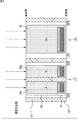
- FIG. 7 shows a cross-sectional view of the normal pixel 120 (Gb pixel) and the phase difference pixel 121 in the central portion of the angle of view shown in FIG. 5, and FIG. 8 shows the normal pixel 120 (in the peripheral portion of the angle of view shown in FIG. A cross-sectional view of the Gb pixel) and the phase difference pixel 121 is shown.
- the photodiode (PD1) in the phase difference pixel 121A performs photoelectric conversion with the first region R1, which is a main part of charge accumulation, and moves to the main part.
- the second region R2 that contributes to the charge transfer is formed.
- the photodiode (PD2) in the phase difference pixel 121B is formed of the first region R1 and the second region R2.
- the impurity concentration is represented by shading, and the impurity concentration in the first region R1 is higher than the impurity concentration in the second region R2.
- the ratio of the second region R2 to the entire region is larger than that of the first region R1.
- the phase difference pixel 121 changes the size of the light receiving surface according to the image height, it is not necessary to change the width of the second region R2 on the light incident side (back side) at the center of the angle of view. However, it is necessary to narrow the width of the second region R2 in the periphery of the angle of view. That is, as shown in FIG. 8, in the periphery of the angle of view, the width of the second region R2 of the photodiode (PD1) in the phase difference pixel 121A is equal to the second region of the photodiode (PD2) in the phase difference pixel 121B. It is formed to be narrower than the width of R2.
- the width of the first region R1 of the photodiode (PD1) and the photodiode (PD2) in the periphery of the angle of view are the same as in the center of the angle of view.
- the first regions R1 are formed to have the same width.
- the element isolation part responsible for element isolation of each pixel is formed by dividing it into an element isolation part 151 on the back surface side and an element isolation part 152 on the front surface side, and the element isolation part 151 has an angle of view center and an angle of view.
- the element isolation portion 152 makes the width of the first region R1 the same at the central portion of the view angle and the peripheral portion of the view angle.
- each phase difference pixel 121 arranged in the pixel array unit 111 can be made constant.
- the element isolation part 151 and the element isolation part 152 can be formed with a metal, an oxide film, or an impurity, for example.
- the first region R1 and the second region R2 have the same configuration in the phase difference pixel 121A and the phase difference pixel 121B in the center of the angle of view in FIG.
- the configuration of the second region R2 is different, but the first region R1 has the same configuration so as not to cause a large difference in the saturation signal amount and the ease of transfer.
- the characteristics of the respective phase difference pixels 121 arranged in the array unit 111 are made constant.
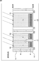
- FIG. 9 is a plan view of the normal pixel 120 (Gb pixel) and the phase difference pixel 121 in the center of the angle of view shown in FIG. 5, and FIG. 10 is a diagram of the normal pixel 120 (in the periphery of the angle of view shown in FIG. A plan view of the Gb pixel) and the phase difference pixel 121 is shown.
- the photodiode (PD1) in the phase difference pixel 121A is connected to the first region R1 that is a main part of charge accumulation.
- the second region R2 is formed from the second region R2 that performs photoelectric conversion and contributes to charge transfer to the main part.
- the photodiode (PD2) in the phase difference pixel 121B is formed of the first region R1 and the second region R2.
- the impurity concentration in each photodiode (PD1, PD2) is represented by shading as in FIGS.
- the transfer transistor (TR1) is parallel to the direction in which the phase difference pixel 121A and the phase difference pixel 121B are divided, and is located closest to the center of the light receiving surface of the photodiode (PD1). Located in the vicinity. As a result, the impurity concentration in the region near the transfer transistor (TR1) is higher than the impurity concentration in other regions.
- the transfer transistor (TR2) is parallel to the direction in which the phase difference pixel 121A and the phase difference pixel 121B are divided and is closest to the center of the light receiving surface of the photodiode (PD2). It is arranged in the vicinity of As a result, the impurity concentration in the region near the transfer transistor (TR2) is higher than the impurity concentration in other regions.
- the phase difference pixel 121 changes the size of the light receiving surface according to the image height, it is not necessary to change the size of the light receiving surface at the center of the angle of view, but changes the size of the light receiving surface at the periphery of the angle of view. There is a need. That is, as shown in FIG. 10, in the periphery of the angle of view, the size of the light receiving surface in the phase difference pixel 121A is smaller than the size of the light receiving surface in the phase difference pixel 121B. However, by arranging transfer transistors (TR1, TR2) in the periphery of the angle of view in the same manner as in the center of the angle of view, the impurity concentration in the area near these transfer transistors (TR1, TR2) The impurity concentration is higher.
- each phase difference pixel 121 even if the size of the light receiving surface changes continuously according to the image height, for example, the size of the light receiving surface in the phase difference pixel 121A is reduced, the first region having a high impurity concentration. It is unchanged that R1 is formed in a region near the transfer transistor (TR1). As a result, since the first region R1 having a high impurity concentration is not affected by the change in size, there are large differences in the saturation signal amount and the ease of transfer in the peripheral portion of the angle of view compared to the central portion of the angle of view. Therefore, the characteristics of each phase difference pixel 121 arranged in the pixel array unit 111 can be made constant.
- the structure of the vicinity of the transfer transistors (TR1, TR2) is changed in the central part of the angle of view in FIG. 9 and the peripheral part of the angle of view in FIG.
- TR1, TR2 the transfer transistors
- the characteristics of each phase difference pixel 121 arranged in the pixel array unit 111 are made constant.
- the present technology in each of the phase difference pixels 121 arranged in the pixel array unit 111, when the size of the light receiving surface is continuously changed according to the image height, the first region having a high impurity concentration.
- the difference between the saturation signal amount and the ease of transfer does not occur in the peripheral portion of the view angle as compared with the center portion of the view angle.
- the characteristics of the pixel 121 can be made constant. That is, in each phase difference pixel 121, since the main part of charge accumulation has the same structure, it is possible to achieve both the pupil correction and the suppression of the decrease in the saturation signal amount and to perform the charge transfer in the same manner.
- phase difference pixel 121 since the phase difference pixel 121A and the phase difference pixel 121B are mounted in one pixel as a pair, the phase difference pixel 121 that is easily arranged in the pixel array unit 111 is easily provided. Therefore, the characteristics of the phase difference pixel 121 can be improved. Further, since the sizes of the phase difference pixels 121A and 121B are changed according to the image height in accordance with the pupil correction of the lens, as a result, the number of interchangeable lenses that can cope with the image plane phase difference AF can be increased.
- phase difference pixels 121 arranged in rows in the pixel array unit 111 have been described.
- the present technology can also be applied to the case where the phase difference pixels 121 are arranged in columns.
- the phase difference pixels 121A and 121B have the same size light receiving surface at the center of the angle of view, but the size of the light receiving surface changes according to the image height at the periphery of the angle of view. become.
- each phase difference pixel 121 is configured to have the size of.
- the present technology is not limited to application to a solid-state image sensor. That is, the present technology provides a solid-state imaging device for an image capturing unit (photoelectric conversion unit) such as an imaging device such as a digital camera, a portable terminal device having an imaging function, and a copying machine using a solid-state imaging device for an image reading unit. Applicable to all electronic devices used.
- the solid-state imaging device may be formed as a single chip, or may be a module-shaped configuration having an imaging function in which an imaging unit and a signal processing unit or an optical system are packaged together. Good.
- FIG. 11 is a block diagram illustrating a configuration of an embodiment of an electronic device to which the present technology is applied.
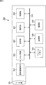
- an imaging apparatus 300 as an electronic device includes an optical unit 301 including a lens group and the like, a solid-state imaging device 302 in which each configuration of the unit pixel 120 described above is employed, and a camera signal processing circuit.
- a DSP (Digital Signal Processor) circuit 303 is provided.
- the imaging apparatus 300 also includes a frame memory 304, a display unit 305, a recording unit 306, an operation unit 307, a power supply unit 308, and a control unit 309.
- the DSP circuit 303, the frame memory 304, the display unit 305, the recording unit 306, the operation unit 307, the power supply unit 308, and the control unit 309 are connected to each other via the bus line 310.
- the optical unit 301 takes in incident light (image light) from a subject and forms an image on the imaging surface of the solid-state imaging device 302.
- the solid-state imaging device 302 converts the amount of incident light imaged on the imaging surface by the optical unit 301 into an electrical signal in units of pixels, and outputs a color component signal for forming an image signal indicating an image of a subject. Output as a signal. Further, the solid-state imaging device 302 outputs a phase difference detection signal used for the image plane phase difference AF as a pixel signal.
- a solid-state imaging device such as the CMOS image sensor 100 according to the above-described embodiment, that is, a solid-state imaging device capable of making the characteristics of each phase difference pixel 121 arranged in the pixel array unit 111 constant. Can be used.
- the display unit 305 includes a panel type display device such as a liquid crystal panel or an organic EL (electroluminescence) panel, and displays a still image or a moving image captured by the solid-state image sensor 302.
- the recording unit 306 records still image or moving image data captured by the solid-state imaging element 302 in a recording medium such as a flash memory.
- the operation unit 307 issues operation commands for various functions of the imaging apparatus 300 in accordance with user operations.
- the power supply unit 308 appropriately supplies various power sources serving as operation power sources for the DSP circuit 303, the frame memory 304, the display unit 305, the recording unit 306, the operation unit 307, and the control unit 309 to these supply targets.
- the control unit 309 controls the operation of each unit of the imaging apparatus 300.
- the control unit 309 calculates a defocus amount by performing a predetermined calculation using the phase difference detection signal from the solid-state imaging element 302, and is in a focused state according to the defocus amount. Controls driving of a photographic lens included in the optical unit 301. Thereby, image plane phase difference AF is performed, and the subject is focused.
- the present invention is applied to a CMOS image sensor in which unit pixels that detect signal charges according to the amount of visible light as physical quantities are arranged in a matrix has been described as an example.
- the present technology is not limited to application to a CMOS image sensor, and can be applied to all column-type solid-state imaging devices in which a column processing unit is arranged for each pixel column of a pixel array unit.
- the present technology is not limited to application to a solid-state imaging device that detects the distribution of the amount of incident light of visible light and captures it as an image, but a solid-state that captures the distribution of the incident amount of infrared rays, X-rays, particles, or the like as an image.
- solid-state imaging devices physical quantity distribution detection devices
- fingerprint detection sensors that detect the distribution of other physical quantities such as pressure and capacitance and capture images as images.
- the present technology can take the following configurations.
- a pixel in which a light receiving surface has a pair of first and second photoelectric conversion units each having a size corresponding to an image height, and second pixels from which phase difference detection signals are obtained are arranged in a matrix.
- the pair of the first photoelectric conversion unit and the second photoelectric conversion unit are a first region that is a main part of charge accumulation and a second region that performs photoelectric conversion and contributes to charge transfer to the main part.
- a solid-state image sensor having regions.
- the second region on the light incident side has a size corresponding to pupil correction, and the second region on the opposite side of the light incident side.
- region of 1 becomes the same size.
- the solid-state imaging device according to (1) which is higher than the impurity concentration.
- the first transfer transistor is disposed in the vicinity of the position closest to the center of the light receiving surface of the first photoelectric conversion unit, The solid-state imaging device according to (5), wherein the second transfer transistor is disposed in a vicinity of a position closest to a center of a light receiving surface of the second photoelectric conversion unit.
- a pair of said 1st photoelectric conversion part and said 2nd photoelectric conversion part are isolate
- the solid-state image sensor as described in any one of (1) thru
- (11) A first pixel that has a photoelectric conversion unit that receives incident light and performs photoelectric conversion, and obtains a color component signal;
- the pair of the first photoelectric conversion unit and the second photoelectric conversion unit are a first region that is a main part of charge accumulation and a second region that performs photoelectric conversion and contributes to charge transfer to the main part.
- the pixel driving unit separately drives the pair of the first photoelectric conversion unit and the second photoelectric conversion unit, and simultaneously performs exposure and transfer in the first photoelectric conversion unit and the second photoelectric conversion unit.
- a driving method including the step of performing.
- a first pixel that has a photoelectric conversion unit that receives incident light and performs photoelectric conversion, and obtains a color component signal;
- a pixel in which a light receiving surface has a pair of first and second photoelectric conversion units each having a size corresponding to an image height, and second pixels from which phase difference detection signals are obtained are arranged in a matrix.
- the pair of the first photoelectric conversion unit and the second photoelectric conversion unit are a first region that is a main part of charge accumulation and a second region that performs photoelectric conversion and contributes to charge transfer to the main part. Equipped with a solid-state image sensor that has each area,
- An electronic apparatus comprising a control unit that controls an image plane phase difference AF (Autofocus) using the phase difference detection signal output from the solid-state imaging device.
- CMOS image sensor 111 pixel array unit, 120 normal pixel, 121, 121A, 121B phase difference pixel, 151, 152 element separation unit, 300 imaging device, 302 solid-state imaging device, 309 control unit, R1 first area, R2 Second region, PD, PD1, PD2 photodiode, TR, TR1, TR2 transfer transistor, RST, RST1, RST2 reset transistor, AMP, AMP1, AMP2 amplification transistor, SEL, SEL1, SEL2 selection transistor, FDG, FDG1, FDG2 Capacitance switching transistor
Landscapes
- Engineering & Computer Science (AREA)
- Physics & Mathematics (AREA)
- Power Engineering (AREA)
- Multimedia (AREA)
- Signal Processing (AREA)
- General Physics & Mathematics (AREA)
- Condensed Matter Physics & Semiconductors (AREA)
- Electromagnetism (AREA)
- Computer Hardware Design (AREA)
- Microelectronics & Electronic Packaging (AREA)
- Solid State Image Pick-Up Elements (AREA)
- Transforming Light Signals Into Electric Signals (AREA)
- Color Television Image Signal Generators (AREA)
Priority Applications (5)
| Application Number | Priority Date | Filing Date | Title |
|---|---|---|---|
| KR1020167007217A KR101857377B1 (ko) | 2013-09-25 | 2014-09-12 | 고체 촬상 소자 및 그 구동 방법, 및 전자 기기 |
| CN201480048428.1A CN105518862B (zh) | 2013-09-25 | 2014-09-12 | 固态成像器件、固态成像器件的驱动方法及电子装置 |
| US15/022,478 US9706145B2 (en) | 2013-09-25 | 2014-09-12 | Solid-state imaging element and driving method therefor, and electronic apparatus |
| US15/587,035 US9888196B2 (en) | 2013-09-25 | 2017-05-04 | Solid-state imaging element and driving method therefor, and electronic apparatus |
| US15/815,415 US10015426B2 (en) | 2013-09-25 | 2017-11-16 | Solid-state imaging element and driving method therefor, and electronic apparatus |
Applications Claiming Priority (2)
| Application Number | Priority Date | Filing Date | Title |
|---|---|---|---|
| JP2013-197872 | 2013-09-25 | ||
| JP2013197872A JP6127869B2 (ja) | 2013-09-25 | 2013-09-25 | 固体撮像素子及びその駆動方法、並びに電子機器 |
Related Child Applications (2)
| Application Number | Title | Priority Date | Filing Date |
|---|---|---|---|
| US15/022,478 A-371-Of-International US9706145B2 (en) | 2013-09-25 | 2014-09-12 | Solid-state imaging element and driving method therefor, and electronic apparatus |
| US15/587,035 Continuation US9888196B2 (en) | 2013-09-25 | 2017-05-04 | Solid-state imaging element and driving method therefor, and electronic apparatus |
Publications (1)
| Publication Number | Publication Date |
|---|---|
| WO2015045915A1 true WO2015045915A1 (ja) | 2015-04-02 |
Family
ID=52743057
Family Applications (1)
| Application Number | Title | Priority Date | Filing Date |
|---|---|---|---|
| PCT/JP2014/074245 WO2015045915A1 (ja) | 2013-09-25 | 2014-09-12 | 固体撮像素子及びその駆動方法、並びに電子機器 |
Country Status (6)
| Country | Link |
|---|---|
| US (3) | US9706145B2 (zh) |
| JP (1) | JP6127869B2 (zh) |
| KR (1) | KR101857377B1 (zh) |
| CN (3) | CN105518862B (zh) |
| TW (1) | TWI663877B (zh) |
| WO (1) | WO2015045915A1 (zh) |
Cited By (1)
| Publication number | Priority date | Publication date | Assignee | Title |
|---|---|---|---|---|
| EP4376062A3 (en) * | 2016-01-27 | 2024-09-04 | Sony Group Corporation | Solid-state image capture element and electronic device |
Families Citing this family (27)
| Publication number | Priority date | Publication date | Assignee | Title |
|---|---|---|---|---|
| KR20150121564A (ko) * | 2014-04-21 | 2015-10-29 | 삼성전자주식회사 | 촬상 소자 및 촬영 장치 |
| KR102449720B1 (ko) * | 2015-10-12 | 2022-09-29 | 삼성전자주식회사 | 이미지 센서를 이용한 인증 방법 및 장치 |
| CN111741200B (zh) | 2016-04-08 | 2021-12-21 | 佳能株式会社 | 图像传感器和摄像设备 |
| JP6774207B2 (ja) * | 2016-04-08 | 2020-10-21 | キヤノン株式会社 | 撮像素子及び撮像装置 |
| JP7005125B2 (ja) | 2016-04-22 | 2022-01-21 | キヤノン株式会社 | 撮像素子、撮像システム、および撮像素子の製造方法 |
| KR20180024604A (ko) | 2016-08-30 | 2018-03-08 | 삼성전자주식회사 | 이미지 센서 및 그 구동 방법 |
| WO2018061497A1 (ja) * | 2016-09-27 | 2018-04-05 | 富士フイルム株式会社 | 撮像素子及び撮像装置 |
| CN115863370A (zh) * | 2016-10-28 | 2023-03-28 | 索尼公司 | 光检测装置 |
| KR102574236B1 (ko) * | 2016-12-07 | 2023-09-05 | 에스케이하이닉스 주식회사 | 서로 다른 사이즈의 포토다이오드들을 갖는 이미지 센서 |
| TWI754696B (zh) * | 2016-12-14 | 2022-02-11 | 日商索尼半導體解決方案公司 | 固體攝像元件及電子機器 |
| JP6877166B2 (ja) * | 2017-02-10 | 2021-05-26 | ユナイテッド・セミコンダクター・ジャパン株式会社 | 半導体装置及びその製造方法 |
| JP6932580B2 (ja) * | 2017-08-04 | 2021-09-08 | ソニーセミコンダクタソリューションズ株式会社 | 固体撮像素子 |
| US11658193B2 (en) | 2018-01-23 | 2023-05-23 | Samsung Electronics Co., Ltd. | Image sensor |
| US10714517B2 (en) * | 2018-01-23 | 2020-07-14 | Samsung Electronics Co., Ltd. | Image sensor |
| JP2019140219A (ja) * | 2018-02-09 | 2019-08-22 | ソニーセミコンダクタソリューションズ株式会社 | 半導体装置および半導体装置の製造方法 |
| KR102532003B1 (ko) | 2018-10-31 | 2023-05-15 | 에스케이하이닉스 주식회사 | 하나의 포토다이오드를 공유하는 두 색의 컬러 필터들을 가진 이미지 센서 |
| CN109713002B (zh) * | 2018-12-07 | 2021-08-31 | 德淮半导体有限公司 | 图像传感器及其形成方法 |
| JP2020113573A (ja) | 2019-01-08 | 2020-07-27 | キヤノン株式会社 | 光電変換装置 |
| KR102519712B1 (ko) | 2019-01-18 | 2023-04-06 | 삼성전자주식회사 | 이미지 센서 |
| JP7555703B2 (ja) | 2019-02-25 | 2024-09-25 | キヤノン株式会社 | 光電変換装置、撮像システム及び移動体 |
| CN110062144A (zh) * | 2019-05-14 | 2019-07-26 | 德淮半导体有限公司 | 相位对焦图像传感器及其形成方法、工作方法 |
| CN110233961B (zh) * | 2019-07-30 | 2021-03-05 | Oppo广东移动通信有限公司 | 互补金属氧化物图像传感器及终端 |
| WO2021053940A1 (ja) * | 2019-09-17 | 2021-03-25 | ソニーセミコンダクタソリューションズ株式会社 | 撮像素子及び撮像装置 |
| JP2021068788A (ja) | 2019-10-21 | 2021-04-30 | キヤノン株式会社 | 光電変換装置、光電変換装置の製造方法、および撮像システム |
| KR20210047483A (ko) * | 2019-10-22 | 2021-04-30 | 에스케이하이닉스 주식회사 | 복수의 촬영 모드를 지원하는 이미지 센서 |
| JP2020188267A (ja) * | 2020-07-14 | 2020-11-19 | キヤノン株式会社 | 撮像装置 |
| KR20220139740A (ko) | 2021-04-08 | 2022-10-17 | 삼성전자주식회사 | 오토 포커스 픽셀을 포함하는 이미지 센서 |
Citations (3)
| Publication number | Priority date | Publication date | Assignee | Title |
|---|---|---|---|---|
| JP2004165462A (ja) * | 2002-11-14 | 2004-06-10 | Sony Corp | 固体撮像素子及びその製造方法 |
| JP2012023207A (ja) * | 2010-07-14 | 2012-02-02 | Toshiba Corp | 裏面照射型固体撮像装置 |
| JP2013080797A (ja) * | 2011-10-03 | 2013-05-02 | Canon Inc | 固体撮像装置およびカメラ |
Family Cites Families (21)
| Publication number | Priority date | Publication date | Assignee | Title |
|---|---|---|---|---|
| JP2500428B2 (ja) * | 1993-04-06 | 1996-05-29 | 日本電気株式会社 | イメ―ジセンサおよびその駆動方法 |
| US6563105B2 (en) * | 1999-06-08 | 2003-05-13 | University Of Washington | Image acquisition with depth enhancement |
| US6750437B2 (en) * | 2000-08-28 | 2004-06-15 | Canon Kabushiki Kaisha | Image pickup apparatus that suitably adjusts a focus |
| JP2006294871A (ja) * | 2005-04-11 | 2006-10-26 | Matsushita Electric Ind Co Ltd | 固体撮像装置 |
| JP5002412B2 (ja) * | 2007-10-24 | 2012-08-15 | キヤノン株式会社 | 撮像装置 |
| US8482639B2 (en) * | 2008-02-08 | 2013-07-09 | Omnivision Technologies, Inc. | Black reference pixel for backside illuminated image sensor |
| JP5451111B2 (ja) * | 2008-03-11 | 2014-03-26 | キヤノン株式会社 | 焦点検出装置およびそれを有する撮像装置 |
| JP5552214B2 (ja) * | 2008-03-11 | 2014-07-16 | キヤノン株式会社 | 焦点検出装置 |
| JP5098831B2 (ja) * | 2008-06-06 | 2012-12-12 | ソニー株式会社 | 固体撮像素子およびカメラシステム |
| JP5276371B2 (ja) * | 2008-07-09 | 2013-08-28 | キヤノン株式会社 | 撮像装置 |
| JP5537172B2 (ja) * | 2010-01-28 | 2014-07-02 | ソニー株式会社 | 固体撮像装置及び電子機器 |
| TW201200959A (en) * | 2010-06-29 | 2012-01-01 | Fujifilm Corp | One-eyed stereo photographic device |
| JP2012084816A (ja) | 2010-10-14 | 2012-04-26 | Fujifilm Corp | 裏面照射型撮像素子及び撮像装置 |
| JP5753371B2 (ja) * | 2010-11-25 | 2015-07-22 | キヤノン株式会社 | 撮像装置およびその制御方法 |
| JP5866760B2 (ja) * | 2010-12-16 | 2016-02-17 | 株式会社ニコン | 撮像装置 |
| JP5664270B2 (ja) * | 2011-01-21 | 2015-02-04 | ソニー株式会社 | 撮像素子および撮像装置 |
| JP5750918B2 (ja) * | 2011-02-03 | 2015-07-22 | 株式会社ニコン | 固体撮像素子及びこれを用いた撮像装置 |
| JP2012173531A (ja) * | 2011-02-22 | 2012-09-10 | Sony Corp | 撮像装置、およびフォーカス制御方法、並びにプログラム |
| JP2012182332A (ja) * | 2011-03-02 | 2012-09-20 | Sony Corp | 撮像素子および撮像装置 |
| US8810713B2 (en) * | 2011-07-13 | 2014-08-19 | Olympus Imaging Corp. | Image pickup apparatus and image pickup device for performing auto-focusing |
| JP2013037296A (ja) * | 2011-08-10 | 2013-02-21 | Olympus Imaging Corp | 撮像装置及び撮像素子 |
-
2013
- 2013-09-25 JP JP2013197872A patent/JP6127869B2/ja active Active
-
2014
- 2014-09-02 TW TW103130294A patent/TWI663877B/zh active
- 2014-09-12 US US15/022,478 patent/US9706145B2/en active Active
- 2014-09-12 CN CN201480048428.1A patent/CN105518862B/zh active Active
- 2014-09-12 CN CN201710014175.1A patent/CN107068702B/zh active Active
- 2014-09-12 KR KR1020167007217A patent/KR101857377B1/ko active IP Right Grant
- 2014-09-12 CN CN201710012765.0A patent/CN106888358B/zh active Active
- 2014-09-12 WO PCT/JP2014/074245 patent/WO2015045915A1/ja active Application Filing
-
2017
- 2017-05-04 US US15/587,035 patent/US9888196B2/en active Active
- 2017-11-16 US US15/815,415 patent/US10015426B2/en active Active
Patent Citations (3)
| Publication number | Priority date | Publication date | Assignee | Title |
|---|---|---|---|---|
| JP2004165462A (ja) * | 2002-11-14 | 2004-06-10 | Sony Corp | 固体撮像素子及びその製造方法 |
| JP2012023207A (ja) * | 2010-07-14 | 2012-02-02 | Toshiba Corp | 裏面照射型固体撮像装置 |
| JP2013080797A (ja) * | 2011-10-03 | 2013-05-02 | Canon Inc | 固体撮像装置およびカメラ |
Cited By (1)
| Publication number | Priority date | Publication date | Assignee | Title |
|---|---|---|---|---|
| EP4376062A3 (en) * | 2016-01-27 | 2024-09-04 | Sony Group Corporation | Solid-state image capture element and electronic device |
Also Published As
| Publication number | Publication date |
|---|---|
| TW201515467A (zh) | 2015-04-16 |
| CN105518862B (zh) | 2019-04-05 |
| KR20160060644A (ko) | 2016-05-30 |
| TWI663877B (zh) | 2019-06-21 |
| JP6127869B2 (ja) | 2017-05-17 |
| CN107068702B (zh) | 2020-08-18 |
| JP2015065269A (ja) | 2015-04-09 |
| CN106888358A (zh) | 2017-06-23 |
| US20170237921A1 (en) | 2017-08-17 |
| CN106888358B (zh) | 2020-01-14 |
| CN107068702A (zh) | 2017-08-18 |
| US10015426B2 (en) | 2018-07-03 |
| US9888196B2 (en) | 2018-02-06 |
| US20160234449A1 (en) | 2016-08-11 |
| CN105518862A (zh) | 2016-04-20 |
| US20180077372A1 (en) | 2018-03-15 |
| US9706145B2 (en) | 2017-07-11 |
| KR101857377B1 (ko) | 2018-05-11 |
Similar Documents
| Publication | Publication Date | Title |
|---|---|---|
| JP6127869B2 (ja) | 固体撮像素子及びその駆動方法、並びに電子機器 | |
| JP6965950B2 (ja) | 撮像素子 | |
| JP6789820B2 (ja) | 固体撮像素子およびその製造方法、並びに電子機器 | |
| JP6369233B2 (ja) | 固体撮像素子及びその信号処理方法、並びに電子機器 | |
| US8319874B2 (en) | Connection/separation element in photoelectric converter portion, solid-state imaging device, and imaging apparatus | |
| KR102337317B1 (ko) | 고체 촬상 장치 및 그 구동 방법, 및 전자 기기 | |
| US20090086063A1 (en) | Solid-state imaging device and imaging apparatus using the same | |
| CN113676679B (zh) | 摄像装置和摄像系统 | |
| JP2014107596A (ja) | 撮像素子および撮像ユニット | |
| JP6413233B2 (ja) | 撮像装置および撮像素子 | |
| JP5750918B2 (ja) | 固体撮像素子及びこれを用いた撮像装置 | |
| US10944926B2 (en) | Solid-state imaging element, method for driving solid-state imaging element, and electronic apparatus | |
| TW201507482A (zh) | 固體攝像元件及其驅動方法與電子機器 | |
| JP2018207544A (ja) | 撮像装置および撮像素子 | |
| JP2010193502A (ja) | 撮像装置 |
Legal Events
| Date | Code | Title | Description |
|---|---|---|---|
| 121 | Ep: the epo has been informed by wipo that ep was designated in this application |
Ref document number: 14848046 Country of ref document: EP Kind code of ref document: A1 |
|
| WWE | Wipo information: entry into national phase |
Ref document number: 15022478 Country of ref document: US |
|
| ENP | Entry into the national phase |
Ref document number: 20167007217 Country of ref document: KR Kind code of ref document: A |
|
| NENP | Non-entry into the national phase |
Ref country code: DE |
|
| 122 | Ep: pct application non-entry in european phase |
Ref document number: 14848046 Country of ref document: EP Kind code of ref document: A1 |