WO2015045531A1 - 絶縁ゲート型半導体装置 - Google Patents
絶縁ゲート型半導体装置 Download PDFInfo
- Publication number
- WO2015045531A1 WO2015045531A1 PCT/JP2014/066907 JP2014066907W WO2015045531A1 WO 2015045531 A1 WO2015045531 A1 WO 2015045531A1 JP 2014066907 W JP2014066907 W JP 2014066907W WO 2015045531 A1 WO2015045531 A1 WO 2015045531A1
- Authority
- WO
- WIPO (PCT)
- Prior art keywords
- voltage
- insulated gate
- gate semiconductor
- semiconductor element
- output current
- Prior art date
- Legal status (The legal status is an assumption and is not a legal conclusion. Google has not performed a legal analysis and makes no representation as to the accuracy of the status listed.)
- Ceased
Links
Images


Classifications
-
- H—ELECTRICITY
- H02—GENERATION; CONVERSION OR DISTRIBUTION OF ELECTRIC POWER
- H02M—APPARATUS FOR CONVERSION BETWEEN AC AND AC, BETWEEN AC AND DC, OR BETWEEN DC AND DC, AND FOR USE WITH MAINS OR SIMILAR POWER SUPPLY SYSTEMS; CONVERSION OF DC OR AC INPUT POWER INTO SURGE OUTPUT POWER; CONTROL OR REGULATION THEREOF
- H02M1/00—Details of apparatus for conversion
- H02M1/08—Circuits specially adapted for the generation of control voltages for semiconductor devices incorporated in static converters
- H02M1/088—Circuits specially adapted for the generation of control voltages for semiconductor devices incorporated in static converters for the simultaneous control of series or parallel connected semiconductor devices
-
- H—ELECTRICITY
- H02—GENERATION; CONVERSION OR DISTRIBUTION OF ELECTRIC POWER
- H02M—APPARATUS FOR CONVERSION BETWEEN AC AND AC, BETWEEN AC AND DC, OR BETWEEN DC AND DC, AND FOR USE WITH MAINS OR SIMILAR POWER SUPPLY SYSTEMS; CONVERSION OF DC OR AC INPUT POWER INTO SURGE OUTPUT POWER; CONTROL OR REGULATION THEREOF
- H02M1/00—Details of apparatus for conversion
- H02M1/08—Circuits specially adapted for the generation of control voltages for semiconductor devices incorporated in static converters
-
- H—ELECTRICITY
- H02—GENERATION; CONVERSION OR DISTRIBUTION OF ELECTRIC POWER
- H02M—APPARATUS FOR CONVERSION BETWEEN AC AND AC, BETWEEN AC AND DC, OR BETWEEN DC AND DC, AND FOR USE WITH MAINS OR SIMILAR POWER SUPPLY SYSTEMS; CONVERSION OF DC OR AC INPUT POWER INTO SURGE OUTPUT POWER; CONTROL OR REGULATION THEREOF
- H02M7/00—Conversion of AC power input into DC power output; Conversion of DC power input into AC power output
-
- H—ELECTRICITY
- H02—GENERATION; CONVERSION OR DISTRIBUTION OF ELECTRIC POWER
- H02M—APPARATUS FOR CONVERSION BETWEEN AC AND AC, BETWEEN AC AND DC, OR BETWEEN DC AND DC, AND FOR USE WITH MAINS OR SIMILAR POWER SUPPLY SYSTEMS; CONVERSION OF DC OR AC INPUT POWER INTO SURGE OUTPUT POWER; CONTROL OR REGULATION THEREOF
- H02M7/00—Conversion of AC power input into DC power output; Conversion of DC power input into AC power output
- H02M7/02—Conversion of AC power input into DC power output without possibility of reversal
- H02M7/04—Conversion of AC power input into DC power output without possibility of reversal by static converters
- H02M7/12—Conversion of AC power input into DC power output without possibility of reversal by static converters using discharge tubes with control electrode or semiconductor devices with control electrode
- H02M7/21—Conversion of AC power input into DC power output without possibility of reversal by static converters using discharge tubes with control electrode or semiconductor devices with control electrode using devices of a triode or transistor type requiring continuous application of a control signal
-
- H—ELECTRICITY
- H02—GENERATION; CONVERSION OR DISTRIBUTION OF ELECTRIC POWER
- H02M—APPARATUS FOR CONVERSION BETWEEN AC AND AC, BETWEEN AC AND DC, OR BETWEEN DC AND DC, AND FOR USE WITH MAINS OR SIMILAR POWER SUPPLY SYSTEMS; CONVERSION OF DC OR AC INPUT POWER INTO SURGE OUTPUT POWER; CONTROL OR REGULATION THEREOF
- H02M7/00—Conversion of AC power input into DC power output; Conversion of DC power input into AC power output
- H02M7/42—Conversion of DC power input into AC power output without possibility of reversal
- H02M7/44—Conversion of DC power input into AC power output without possibility of reversal by static converters
- H02M7/48—Conversion of DC power input into AC power output without possibility of reversal by static converters using discharge tubes with control electrode or semiconductor devices with control electrode
- H02M7/53—Conversion of DC power input into AC power output without possibility of reversal by static converters using discharge tubes with control electrode or semiconductor devices with control electrode using devices of a triode or transistor type requiring continuous application of a control signal
- H02M7/537—Conversion of DC power input into AC power output without possibility of reversal by static converters using discharge tubes with control electrode or semiconductor devices with control electrode using devices of a triode or transistor type requiring continuous application of a control signal using semiconductor devices only, e.g. single switched pulse inverters
- H02M7/5387—Conversion of DC power input into AC power output without possibility of reversal by static converters using discharge tubes with control electrode or semiconductor devices with control electrode using devices of a triode or transistor type requiring continuous application of a control signal using semiconductor devices only, e.g. single switched pulse inverters in a bridge configuration
- H02M7/53871—Conversion of DC power input into AC power output without possibility of reversal by static converters using discharge tubes with control electrode or semiconductor devices with control electrode using devices of a triode or transistor type requiring continuous application of a control signal using semiconductor devices only, e.g. single switched pulse inverters in a bridge configuration with automatic control of output voltage or current
-
- H—ELECTRICITY
- H03—ELECTRONIC CIRCUITRY
- H03K—PULSE TECHNIQUE
- H03K17/00—Electronic switching or gating, i.e. not by contact-making and –breaking
- H03K17/06—Modifications for ensuring a fully conducting state
-
- H—ELECTRICITY
- H03—ELECTRONIC CIRCUITRY
- H03K—PULSE TECHNIQUE
- H03K17/00—Electronic switching or gating, i.e. not by contact-making and –breaking
- H03K17/08—Modifications for protecting switching circuit against overcurrent or overvoltage
- H03K17/082—Modifications for protecting switching circuit against overcurrent or overvoltage by feedback from the output to the control circuit
- H03K17/0828—Modifications for protecting switching circuit against overcurrent or overvoltage by feedback from the output to the control circuit in composite switches
-
- H—ELECTRICITY
- H02—GENERATION; CONVERSION OR DISTRIBUTION OF ELECTRIC POWER
- H02M—APPARATUS FOR CONVERSION BETWEEN AC AND AC, BETWEEN AC AND DC, OR BETWEEN DC AND DC, AND FOR USE WITH MAINS OR SIMILAR POWER SUPPLY SYSTEMS; CONVERSION OF DC OR AC INPUT POWER INTO SURGE OUTPUT POWER; CONTROL OR REGULATION THEREOF
- H02M1/00—Details of apparatus for conversion
- H02M1/32—Means for protecting converters other than automatic disconnection
- H02M1/327—Means for protecting converters other than automatic disconnection against abnormal temperatures
-
- H—ELECTRICITY
- H02—GENERATION; CONVERSION OR DISTRIBUTION OF ELECTRIC POWER
- H02M—APPARATUS FOR CONVERSION BETWEEN AC AND AC, BETWEEN AC AND DC, OR BETWEEN DC AND DC, AND FOR USE WITH MAINS OR SIMILAR POWER SUPPLY SYSTEMS; CONVERSION OF DC OR AC INPUT POWER INTO SURGE OUTPUT POWER; CONTROL OR REGULATION THEREOF
- H02M7/00—Conversion of AC power input into DC power output; Conversion of DC power input into AC power output
- H02M7/42—Conversion of DC power input into AC power output without possibility of reversal
- H02M7/44—Conversion of DC power input into AC power output without possibility of reversal by static converters
- H02M7/48—Conversion of DC power input into AC power output without possibility of reversal by static converters using discharge tubes with control electrode or semiconductor devices with control electrode
- H02M7/53—Conversion of DC power input into AC power output without possibility of reversal by static converters using discharge tubes with control electrode or semiconductor devices with control electrode using devices of a triode or transistor type requiring continuous application of a control signal
- H02M7/537—Conversion of DC power input into AC power output without possibility of reversal by static converters using discharge tubes with control electrode or semiconductor devices with control electrode using devices of a triode or transistor type requiring continuous application of a control signal using semiconductor devices only, e.g. single switched pulse inverters
- H02M7/5387—Conversion of DC power input into AC power output without possibility of reversal by static converters using discharge tubes with control electrode or semiconductor devices with control electrode using devices of a triode or transistor type requiring continuous application of a control signal using semiconductor devices only, e.g. single switched pulse inverters in a bridge configuration
-
- H—ELECTRICITY
- H03—ELECTRONIC CIRCUITRY
- H03K—PULSE TECHNIQUE
- H03K17/00—Electronic switching or gating, i.e. not by contact-making and –breaking
- H03K17/08—Modifications for protecting switching circuit against overcurrent or overvoltage
- H03K2017/0806—Modifications for protecting switching circuit against overcurrent or overvoltage against excessive temperature
Definitions
- the present invention relates to an insulated gate semiconductor device that supplies power to a load by switching an insulated gate semiconductor element such as an IGBT or a power MOS-FET.
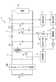
- FIG. 4 is a schematic configuration diagram of a main part showing an example of this type of semiconductor device 1 introduced in detail in, for example, Patent Document 1.
- FIG. 4 is a schematic configuration diagram of a main part showing an example of this type of semiconductor device 1 introduced in detail in, for example, Patent Document 1.
- the semiconductor device 1 includes a diode bridge circuit DB that rectifies input AC power AC, and a converter 2 that converts the output of the diode bridge circuit DB into DC power having a predetermined voltage.
- the semiconductor device 1 further includes a chopper circuit 3 that boosts the DC power obtained from the converter 2 and supplies the boosted DC power to a load RL such as a motor.
- the converter 2 includes a switching element S1 made of, for example, a MOS-FET for switching the output of the diode bridge circuit DB at a predetermined frequency via the primary winding of the insulating transformer T. Further, the converter 2 includes a rectifying / smoothing circuit including a diode D1 that rectifies and outputs a voltage generated in the secondary winding of the insulating transformer T, and a capacitor C1 that smoothes the output of the diode D1.
- the flyback converter 2 configured as described above controls the output voltage generated in the secondary winding of the isolation transformer T by controlling the ON width of the switching element S1, for example, by the main control unit 4. To do.
- the chopper circuit 3 includes an inductor L to which the output voltage of the converter 2 is applied, and a switching element S2 that controls a current flowing through the inductor L.
- the switching element S ⁇ b> 2 is turned on when a predetermined gate voltage is applied from the driving unit 5 and accumulates power energy in the inductor L.
- the power energy accumulated in the inductor L is discharged from the inductor L by the off operation of the switching element S2.
- the power energy released from the inductor L is stored in the capacitor C2 via the diode D2, and then supplied to the load RL as a DC voltage.
- the switching element S2 is composed of, for example, a junction FET used in a unipolar mode with good high-speed followability.
- the semiconductor device 1 includes a current detection unit 6 that detects an output current supplied from the chopper circuit 3 to the load RL or a current flowing through the switching element S2.
- the current detection unit 6 plays a role of detecting whether or not the current supplied to the load RL exceeds a preset threshold value, that is, an overcurrent.
- the voltage control unit 7 sets the gate voltage output from the driving unit 5 higher than the built-in voltage of the switching element S2 when an overcurrent is detected by the current detection unit 6, so that the switching element S2 is driven in the bipolar mode. In this way, the on-resistance of the switching element S2 can be kept low by operating the switching element S2 in the bipolar mode when overcurrent is detected. And the overheat destruction of the said switching element S2 by overcurrent is prevented.
- 8 is a temperature monitor circuit that detects the operating temperature of the switching element S2 from the current flowing through the gate of the switching element S2 detected through the resistor R.
- the on widths of the switching elements S1 and S2 are feedback-controlled according to the operating temperature of the switching element S2 detected by the temperature monitor unit 8, and the output voltage to the load RL is stabilized.
- the semiconductor device 1 configured using a junction FET as the switching element S2
- an insulated gate semiconductor element such as an IGBT or a MOS-FET having a large short-circuit resistance has been widely used exclusively as the switching element S2.
- the insulated gate semiconductor element unlike the above-described junction FET, the insulated gate semiconductor element cannot be operated by switching between the unipolar mode and the bipolar mode.
- the load RL is an inductive load such as a motor
- a large current temporarily flows through the motor when the motor is started.
- the semiconductor device 1 it is generally necessary to adopt an insulated gate semiconductor element having a large short-circuit resistance in consideration of a current that flows when the motor is started.
- an insulated gate semiconductor element having a large short-circuit tolerance is large and expensive. Therefore, it is desired to realize a drive device that drives the motor by employing an insulated gate semiconductor element suitable for the rated power capacity of the motor.
- the present invention has been made in consideration of such circumstances, and its purpose is to prevent temporary overcurrent generated in the load even when the input power is switched to supply power to an inductive load such as a motor.
- An object of the present invention is to provide an insulated gate semiconductor device having a simple configuration capable of preventing overheat destruction of an insulated gate semiconductor element.
- an insulated gate semiconductor device includes: An insulated gate semiconductor element made of IGBT or power MOS-FET, which receives the first gate voltage determined according to the output specification at the control terminal and is turned on, switches the input voltage and outputs it to the load; An output current detecting means for detecting an output current output to the load in accordance with the switching operation of the insulated gate semiconductor element; Voltage detecting means for detecting the on-voltage of the insulated gate semiconductor element as the collector-emitter voltage Vce of the IGBT or the drain-source voltage Vds of the power MOS-FET;
- the insulated gate semiconductor device has a control terminal of the insulated gate semiconductor element when the output current exceeds a rated current value and the on-voltage is lower than a predetermined first threshold voltage.
- a heat generation amount suppressing means for suppressing a heat generation amount of the insulated gate semiconductor element by setting a gate voltage applied to the first gate voltage higher than that of the first gate voltage.
- the present invention focuses on the on-voltage of the insulated gate semiconductor element at the time of overcurrent detection.
- the on-voltage is lower than the first threshold voltage, for example, it is a temporary overcurrent at the time of starting the motor.
- the gate voltage applied to the control terminal of the insulated gate semiconductor element is set higher than the first gate voltage applied to the control terminal of the insulated gate semiconductor element during normal operation when no overcurrent occurs.
- the on-resistance of the insulated gate semiconductor element is set lower than that during normal operation, and overheat destruction of the insulated gate semiconductor element is prevented.
- the first threshold voltage is set, for example, as approximately twice the ON voltage of the insulated gate semiconductor element when the output current is a rated current.
- the output current exceeds a rated current value, and the on-voltage is more than a second threshold voltage determined according to a maximum rated voltage of the insulated gate semiconductor element.
- the output current is reduced by setting a gate voltage applied to the control terminal of the insulated gate semiconductor element lower than the first gate voltage.
- the gate voltage applied to the control terminal of the insulated gate semiconductor element is set to be low so that the output current is narrowed or cut off to protect the insulated gate semiconductor element from overcurrent.
- the second threshold voltage is set, for example, as approximately 1 ⁇ 2 of the maximum rated voltage of the insulated gate semiconductor element.
- the increase in output current is temporary depending on the load state or due to a load short circuit. Determine if there is.
- the ON voltage is lower than the first threshold voltage and the increase in the output current is temporary, the gate voltage applied to the control terminal of the insulated gate semiconductor element is increased to increase the insulation gate.
- the on-resistance of the semiconductor device As a result, heat generation of the insulated gate semiconductor element due to an increase in output current can be prevented, and overheat destruction can be prevented.
- an insulated gate semiconductor device using an insulated gate semiconductor element having an excess current capacity compared to the rated current for example, in anticipation of a temporary increase in output current according to the load state No need to build.
- a temporary increase in output current is detected from the on-voltage of the insulated gate semiconductor element, the detection itself is simple and reliable. Therefore, it is possible to easily realize an insulated gate semiconductor device that operates stably against a temporary change in load by using a small and inexpensive insulated gate semiconductor element according to the output specifications.
- the short-circuit of the load is detected from an abnormal increase in the on-voltage of the insulated gate semiconductor element.
- the output current is suppressed or cut off by lowering the gate voltage applied to the control terminal of the insulated gate semiconductor element, the insulated gate type is prevented from overcurrent caused by the short circuit failure of the load.
- the semiconductor element can be effectively protected.
- FIG. 1 The principal part schematic block diagram of the insulated gate semiconductor device which concerns on one Embodiment of this invention.
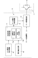
- the schematic block diagram of the drive device of the insulated gate semiconductor element in the insulated gate semiconductor device shown in FIG. The figure which shows the output characteristic of an insulated gate semiconductor element.
- the insulated gate semiconductor device is realized as an inverter device 10 for supplying a driving current to a three-phase AC motor M as shown in FIG.
- the inverter device 10 includes a power semiconductor module packaged with six IGBTs 11a and 11b to 11f as insulated gate semiconductor elements having a large power capacity.
- the six IGBTs 11a, 11b to 11f constitute a main part of the inverter device 10 that drives a three-phase AC motor M as a load.
- the inverter device 10 supplies the drive current to the three-phase AC motor M by driving the plurality of IGBTs 11a, 11b to 11f in association with each other by a control circuit (not shown).
- the six IGBTs 11a, 11b to 11f are connected in series in pairs of two to form three half-bridge circuits HB, respectively. Further, six freewheeling diodes 12a, 12b to 12f are connected in antiparallel to the IGBTs 11a, 11b to 11f, respectively. These three half-bridge circuits HB are connected in parallel to form a three-phase full bridge circuit that drives the three-phase AC motor M.
- reference numerals 13a, 13b to 13f denote drive devices for driving the IGBTs 11a, 11b to 11f on and off, respectively.
- These three half-bridge circuits HB are driven in association with each other, so that the series connection points of the IGBTs 11a and 11d, the series connection points of the IGBTs 11b and 11e, which respectively constitute the half-bridge circuits HB, and From the series connection point of the IGBTs 11c and 11f, a three-phase current consisting of a U-phase, a V-phase, and a W-phase having a phase difference of 120 ° is supplied to the three-phase AC motor M.
- the upper-arm IGBTs 11a, 11b, and 11c and the lower-arm IGBTs 11d, 11e, and 11f in each half-bridge circuit HB are gates with a constant period that are pulse-width modulated from the drive devices 13a, 13b to 13f, respectively.
- each is turned on / off.
- a current corresponding to the pulse width of the gate drive signal is supplied to the three-phase AC motor M through the IGBT 11a (11b, 11c) of the upper arm over a positive half cycle.
- a current corresponding to the pulse width of the control signal is supplied to the three-phase AC motor M through the IGBT 11d (11e, 11f) of the lower arm over a negative half cycle.
- each of the half bridge circuits HB supplies alternating currents whose phases are different from each other by 120 ° to the three-phase alternating current motor M.
- the current supplied to the three-phase AC motor M is a pulse current synchronized with the control signal, and this pulse current forms a discrete sine wave current waveform.
- Each of the driving devices 13 (13a, 13b to 13f) for driving the respective IGBTs 11 (11a, 11b to 11f) on and off receives a gate control signal as shown in FIG.
- a gate drive circuit 14 is provided that generates a gate drive signal of a predetermined voltage and applies the gate drive signal to the gate of the IGBT 11.
- the gate drive signal voltage V GE is generally set to 15 V in accordance with the output characteristics of the IGBT 11 (11a, 11b to 11f).
- the drive device 13 includes an output current detection circuit 15 that detects an output current supplied from the IGBT 11 to the three-phase AC motor M, and a voltage detection circuit 16 that detects a collector-emitter voltage Vce of the IGBT 11. Is provided.
- the output current detection circuit 15 is configured to detect an output current of the IGBT 11 from a current flowing through a current detection emitter provided in the IGBT 11, for example.
- the voltage detection circuit 16 detects the collector-emitter voltage Vce of the IGBT 11 as the ON voltage of the IGBT 11.
- the load state determination circuit 17 provided in the driving device 13 includes an overcurrent detection unit 17a and a voltage determination unit 17b.
- the overcurrent detector 17a determines whether or not the current supplied to the three-phase AC motor M exceeds the rated current by comparing the output current with a predetermined current threshold.
- the voltage determination unit 17b compares the on-voltage of the IGBT 11 when an overcurrent is detected, that is, the collector-emitter voltage Vce, with the first threshold voltage Vth1 and the second threshold voltage Vth2, respectively.
- the first threshold voltage Vth1 is set, for example, as approximately twice the on-voltage of the IGBT 11 when the output current of the IGBT 11 is within the rated current range. Specifically, since the on-voltage of the IGBT 11 during normal operation for outputting a rated current is 2 to 3V, the first threshold voltage Vth1 is set to about 5V.
- the second threshold voltage Vth2 is set, for example, as approximately 1 ⁇ 2 of the maximum rated voltage of the IGBT 11. Specifically, in the case of the IGBT 11 having a maximum rated voltage of 100V, the second threshold voltage Vth2 is set to about 50V.
- the load state determination circuit 17 determines that the collector-emitter voltage Vce detected by the voltage determiner 17b is greater than the first threshold voltage Vth1. If it is lower, for example, it is determined that an overcurrent is temporarily flowing through the three-phase AC motor M when the three-phase AC motor M is started. On the other hand, when the collector-emitter voltage Vce detected by the voltage determination unit 17b is higher than the second threshold voltage Vth2, the load state determination circuit 17 causes the three-phase AC motor M to It is determined that an overcurrent is flowing due to a short circuit.
- the load state determination circuit 17 is a temporary circuit in which the overcurrent is caused by the operating state of the load by paying attention to the collector-emitter voltage Vce of the IGBT 11 when the overcurrent is detected. Or whether it is caused by a short circuit of the load.
- the load state determination circuit 17 controls the gate voltage setting circuit 18 based on the determination result, and changes and sets the gate voltage applied to the IGBT 11 as described below.
- the gate voltage setting circuit 18 which operates in response to the determination result of the load state determination circuit 17 is a voltage of the gate drive signal output from the gate drive circuit 14 when an overcurrent is detected, that is, a gate voltage applied to the IGBT 11.
- the gate voltage setting circuit 18 changes the voltage of the gate drive signal output from the gate drive circuit 14 to be higher than the first gate voltage during normal operation, thereby suppressing the heat generation amount of the IGBT 11. It functions as a suppression means.
- the gate voltage setting circuit 18 functions as output current reduction means for reducing the output current by changing and setting the voltage of the gate drive signal lower than the first gate voltage during normal operation.
- the gate voltage setting circuit 18 when it is determined that the overcurrent is temporary, the gate voltage setting circuit 18 generates a first gate drive signal of 15V output from the gate drive circuit 14 during normal operation. For example, the voltage is set high to 20V. As a result, a gate voltage V GE of 20 V, which is higher than that during normal operation, is applied to the gate of the IGBT 11, and the on-resistance of the IGBT 11 is lowered. As a result, as shown in FIG. 3, the output characteristics of the IGBT 11 are temporarily changed, and a larger current than that during normal operation can be temporarily passed without causing excessive heat generation of the IGBT 11. .
- the gate voltage setting circuit 18 When it is determined that the overcurrent is caused by a short circuit of the three-phase AC motor M, the gate voltage setting circuit 18 outputs the 15V gate drive signal output from the gate drive circuit 14 during normal operation. The voltage is set low, and the current output via the IGBT 11 is suppressed. Preferably, the IGBT 11 is turned off by setting a gate voltage V GE applied to the gate of the IGBT 11 to, for example, 0 V, thereby shutting down the output current and protecting the IGBT 11 from the overcurrent.
- Such voltage control of the gate drive signal can be achieved by changing the drive voltage of a transistor circuit (not shown) constituting the output stage of the gate drive circuit 14.
- the above-mentioned operation is performed while paying attention to the ON voltage of the IGBT 11 when an overcurrent occurs, specifically, the collector-emitter voltage Vce. It is determined whether or not the overcurrent is temporary according to the state of the three-phase AC motor M. In the case of a temporary overcurrent, the on-resistance of the IGBT 11 is lowered by temporarily increasing the voltage of the gate signal applied to the gate of the IGBT 11, thereby reducing the heat generation of the IGBT 11 due to the overcurrent. suppress.
- the inverter device 10 can be constructed using the above. Therefore, the inverter device 10 can be realized at low cost by making full use of the characteristics of the small and inexpensive IGBT 11, and its practical advantages are great.
- the present invention is not limited to the embodiment described above.
- the case where the inverter device 10 is configured as an insulated gate semiconductor device has been described as an example.
- the present invention can be similarly applied to a case where a chopper circuit is configured using the IGBT 11.
- the present invention is also applicable to the case where a power MOS-FET is used as the insulated gate semiconductor.
- the drain-source voltage Vds of the power MOS-FET may be detected as its ON voltage to determine the load state of the three-phase AC motor M at the time of overcurrent.
- the insulated gate semiconductor constituting the inverter device 10 not only a Si-based semiconductor but also a wide band gap semiconductor such as SiC, GaN, or diamond may be applied, and only a part of the insulated gate semiconductor is used. It may be replaced with a wide band gap semiconductor.
- the first threshold voltage Vth1 and the second threshold voltage Vth2 described above may be set according to the specifications and operating characteristics of the insulated gate semiconductor device, the driving conditions of the insulated gate semiconductor element, and the like. Furthermore, it goes without saying that the present invention can be similarly applied to an insulated gate semiconductor device that supplies power to a load other than the three-phase AC motor M. In addition, the present invention can be variously modified and implemented without departing from the scope of the invention.
- Inverter device (insulated gate type semiconductor device) 11, 11a, 11b to 11f IGBT (insulated gate type semiconductor element) 12, 12a, 12b to 12f Free-wheeling diode 13, 13a, 13b to 13f Drive device 14 Gate drive circuit 15 Output current detection circuit 16 Voltage detection circuit 17 Load state determination circuit 17a Overcurrent detection unit 17b Voltage determination unit 18 Gate Voltage setting circuit (heat generation suppression means, output current reduction means) M Three-phase AC motor (load)
Landscapes
- Engineering & Computer Science (AREA)
- Power Engineering (AREA)
- Inverter Devices (AREA)
- Power Conversion In General (AREA)
Abstract
Description
出力仕様に応じて定められた第1のゲート電圧を制御端子に受けてオン動作し、入力電圧をスイッチングして負荷に出力する、IGBTまたはパワーMOS-FETからなる絶縁ゲート型半導体素子と、
この絶縁ゲート型半導体素子のスイッチング動作に伴って前記負荷に出力される出力電流を検出する出力電流検出手段と、
前記絶縁ゲート型半導体素子のオン電圧を、前記IGBTのコレクタ・エミッタ間電圧Vce、または前記パワーMOS-FETのドレイン・ソース間電圧Vdsとして検出する電圧検出手段とを備える。
11,11a,11b~11f IGBT(絶縁ゲート型半導体素子)
12,12a,12b~12f フリーホイリング・ダイオード
13,13a,13b~13f 駆動装置
14 ゲート駆動回路
15 出力電流検出回路
16 電圧検出回路
17 負荷状態判定回路
17a 過電流検出部
17b 電圧判定部
18 ゲート電圧設定回路(発熱量抑制手段,出力電流低減手段)
M 三相交流モータ(負荷)
Claims (6)
- 出力仕様に応じて定められた第1のゲート電圧を制御端子に受けてオン動作し、入力電圧をスイッチングして負荷に出力する絶縁ゲート型半導体素子と、
この絶縁ゲート型半導体素子のスイッチング動作に伴って前記負荷に出力される出力電流を検出する出力電流検出手段と、
前記絶縁ゲート型半導体素子のオン電圧を検出する電圧検出手段と、
前記出力電流が定格出力電流を超え、且つ前記オン電圧が予め定められた第1の閾値電圧よりも低いとき、前記絶縁ゲート型半導体素子の制御端子に加えるゲート電圧を前記第1のゲート電圧よりも高く設定して該絶縁ゲート型半導体素子の発熱量を抑制する発熱量抑制手段と
を具備したことを特徴とする絶縁ゲート型半導体装置。 - 前記絶縁ゲート型半導体素子はIGBTであって、前記電圧検出手段は前記IGBTのコレクタ・エミッタ間電圧Vceを検出するものである請求項1に記載の絶縁ゲート型半導体装置。
- 前記絶縁ゲート型半導体素子はパワーMOS-FETであって、前記電圧検出手段は前記パワーMOS-FETのドレイン・ソース間電圧Vdsを検出するものである請求項1に記載の絶縁ゲート型半導体装置。
- 前記第1の閾値電圧は、前記出力電流が定格電流であるときの前記絶縁ゲート型半導体素子のオン電圧の略2倍として設定される請求項1に記載の絶縁ゲート型半導体装置。
- 請求項1~4のいずれかに記載の絶縁ゲート型半導体装置において、
更に前記出力電流が定格電流を超え、且つ前記オン電圧が前記絶縁ゲート型半導体素子の最大定格電圧に応じて定められた第2の閾値電圧よりも高いとき、該絶縁ゲート型半導体素子の制御端子に加えるゲート電圧を前記第1のゲート電圧よりも低く設定して前記出力電流を低減する出力電流低減手段を備えることを特徴とする絶縁ゲート型半導体装置。 - 前記第2の閾値電圧は、前記絶縁ゲート型半導体素子の最大定格電圧の略1/2として設定される請求項5に記載の絶縁ゲート型半導体装置。
Priority Applications (4)
| Application Number | Priority Date | Filing Date | Title |
|---|---|---|---|
| CN201480020401.1A CN105103427B (zh) | 2013-09-25 | 2014-06-25 | 绝缘栅型半导体装置 |
| JP2015538961A JP6070853B2 (ja) | 2013-09-25 | 2014-06-25 | 絶縁ゲート型半導体装置 |
| DE112014001238.6T DE112014001238T5 (de) | 2013-09-25 | 2014-06-25 | Halbleitervorrichtung mit isoliertem Gate |
| US14/879,553 US10003249B2 (en) | 2013-09-25 | 2015-10-09 | Insulated gate semiconductor device including switchable insulated gate semiconductor element |
Applications Claiming Priority (2)
| Application Number | Priority Date | Filing Date | Title |
|---|---|---|---|
| JP2013-198206 | 2013-09-25 | ||
| JP2013198206 | 2013-09-25 |
Related Child Applications (1)
| Application Number | Title | Priority Date | Filing Date |
|---|---|---|---|
| US14/879,553 Continuation US10003249B2 (en) | 2013-09-25 | 2015-10-09 | Insulated gate semiconductor device including switchable insulated gate semiconductor element |
Publications (1)
| Publication Number | Publication Date |
|---|---|
| WO2015045531A1 true WO2015045531A1 (ja) | 2015-04-02 |
Family
ID=52742689
Family Applications (1)
| Application Number | Title | Priority Date | Filing Date |
|---|---|---|---|
| PCT/JP2014/066907 Ceased WO2015045531A1 (ja) | 2013-09-25 | 2014-06-25 | 絶縁ゲート型半導体装置 |
Country Status (5)
| Country | Link |
|---|---|
| US (1) | US10003249B2 (ja) |
| JP (1) | JP6070853B2 (ja) |
| CN (1) | CN105103427B (ja) |
| DE (1) | DE112014001238T5 (ja) |
| WO (1) | WO2015045531A1 (ja) |
Cited By (2)
| Publication number | Priority date | Publication date | Assignee | Title |
|---|---|---|---|---|
| JP2019161856A (ja) * | 2018-03-13 | 2019-09-19 | 株式会社デンソー | スイッチの駆動回路 |
| JP2022114468A (ja) * | 2021-01-27 | 2022-08-08 | 富士電機株式会社 | モータ駆動装置、モータ駆動方法、およびモータ駆動プログラム |
Families Citing this family (12)
| Publication number | Priority date | Publication date | Assignee | Title |
|---|---|---|---|---|
| GB2545236B (en) * | 2015-12-10 | 2017-12-13 | Rolls Royce Plc | A method of controlling an inverter |
| US9871462B2 (en) * | 2015-12-11 | 2018-01-16 | Phase Technologies, Llc | Regenerative variable frequency drive with auxiliary power supply |
| JP6332304B2 (ja) * | 2016-03-02 | 2018-05-30 | トヨタ自動車株式会社 | Dc−dcコンバータ |
| JP6341222B2 (ja) * | 2016-03-31 | 2018-06-13 | トヨタ自動車株式会社 | 電源システム |
| ES2803198T3 (es) * | 2016-09-01 | 2021-01-25 | Disposición de convertidor así como procedimiento para su funcionamiento | |
| JP6769350B2 (ja) * | 2017-03-08 | 2020-10-14 | 株式会社デンソー | 半導体スイッチの駆動装置 |
| EP3576270A1 (de) * | 2018-05-29 | 2019-12-04 | Siemens Aktiengesellschaft | Umrichterbetrieb mit erhöhter gatesteuerspannung bei hoher sperrschichttemperatur |
| JP6770559B2 (ja) * | 2018-08-29 | 2020-10-14 | 株式会社Subaru | 電力変換装置および車両 |
| CN109600030B (zh) * | 2018-10-12 | 2021-03-23 | 蔚来(安徽)控股有限公司 | 用于功率装置的母线电容放电方法、系统及装置 |
| JP7163486B2 (ja) * | 2019-04-17 | 2022-10-31 | 日立Astemo株式会社 | 負荷駆動装置 |
| JP2021125547A (ja) * | 2020-02-05 | 2021-08-30 | 富士電機株式会社 | 電力用半導体モジュール |
| JP7822298B2 (ja) * | 2022-10-19 | 2026-03-02 | 三菱電機株式会社 | 電力変換装置 |
Citations (2)
| Publication number | Priority date | Publication date | Assignee | Title |
|---|---|---|---|---|
| JP2007259576A (ja) * | 2006-03-23 | 2007-10-04 | Hitachi Ltd | スイッチング素子の駆動回路 |
| JP2010088036A (ja) * | 2008-10-02 | 2010-04-15 | Sumitomo Electric Ind Ltd | 接合型電界効果トランジスタの駆動装置および駆動方法 |
Family Cites Families (7)
| Publication number | Priority date | Publication date | Assignee | Title |
|---|---|---|---|---|
| US6400177B1 (en) * | 2000-01-25 | 2002-06-04 | Matsushita Electric Industrial Co. | Output driver and method for meeting specified output impedance and current characteristics |
| US7245113B2 (en) * | 2004-05-21 | 2007-07-17 | Intersil Corporation | High light load efficiency synchronous buck regulator with pulse skipping control |
| JP5315155B2 (ja) * | 2009-07-23 | 2013-10-16 | 日立オートモティブシステムズ株式会社 | 半導体素子制御装置、車載用電機システム |
| US8937825B2 (en) * | 2009-12-10 | 2015-01-20 | Alfred E. Mann Foundation For Scientific Research | Timing controlled AC to DC converter |
| JP5115829B2 (ja) * | 2010-06-09 | 2013-01-09 | 株式会社デンソー | スイッチング装置 |
| US8885308B2 (en) * | 2011-07-18 | 2014-11-11 | Crane Electronics, Inc. | Input control apparatus and method with inrush current, under and over voltage handling |
| JP5646070B2 (ja) * | 2011-09-13 | 2014-12-24 | 三菱電機株式会社 | 電力用半導体素子のゲート駆動回路、および電力用半導体素子の駆動方法 |
-
2014
- 2014-06-25 CN CN201480020401.1A patent/CN105103427B/zh not_active Expired - Fee Related
- 2014-06-25 JP JP2015538961A patent/JP6070853B2/ja not_active Expired - Fee Related
- 2014-06-25 DE DE112014001238.6T patent/DE112014001238T5/de not_active Withdrawn
- 2014-06-25 WO PCT/JP2014/066907 patent/WO2015045531A1/ja not_active Ceased
-
2015
- 2015-10-09 US US14/879,553 patent/US10003249B2/en active Active
Patent Citations (2)
| Publication number | Priority date | Publication date | Assignee | Title |
|---|---|---|---|---|
| JP2007259576A (ja) * | 2006-03-23 | 2007-10-04 | Hitachi Ltd | スイッチング素子の駆動回路 |
| JP2010088036A (ja) * | 2008-10-02 | 2010-04-15 | Sumitomo Electric Ind Ltd | 接合型電界効果トランジスタの駆動装置および駆動方法 |
Cited By (4)
| Publication number | Priority date | Publication date | Assignee | Title |
|---|---|---|---|---|
| JP2019161856A (ja) * | 2018-03-13 | 2019-09-19 | 株式会社デンソー | スイッチの駆動回路 |
| JP7043903B2 (ja) | 2018-03-13 | 2022-03-30 | 株式会社デンソー | スイッチの駆動回路 |
| JP2022114468A (ja) * | 2021-01-27 | 2022-08-08 | 富士電機株式会社 | モータ駆動装置、モータ駆動方法、およびモータ駆動プログラム |
| JP7686987B2 (ja) | 2021-01-27 | 2025-06-03 | 富士電機株式会社 | モータ駆動装置、モータ駆動方法、およびモータ駆動プログラム |
Also Published As
| Publication number | Publication date |
|---|---|
| DE112014001238T5 (de) | 2016-01-14 |
| JPWO2015045531A1 (ja) | 2017-03-09 |
| JP6070853B2 (ja) | 2017-02-01 |
| US20160036316A1 (en) | 2016-02-04 |
| CN105103427B (zh) | 2018-04-27 |
| CN105103427A (zh) | 2015-11-25 |
| US10003249B2 (en) | 2018-06-19 |
Similar Documents
| Publication | Publication Date | Title |
|---|---|---|
| JP6070853B2 (ja) | 絶縁ゲート型半導体装置 | |
| US10389263B2 (en) | Motor drive with silicon carbide MOSFET switches | |
| JP4445036B2 (ja) | 電力変換器 | |
| US20180145602A1 (en) | Motor drive with silicon carbide mosfet switches | |
| JP5752234B2 (ja) | 電力変換装置 | |
| WO2018158807A1 (ja) | 半導体装置、および、電力変換システム | |
| JP2017534237A (ja) | 抵抗器エミュレーション及びゲートブースト | |
| WO2012105112A1 (ja) | Dc/dcコンバータ | |
| TW201336221A (zh) | 電流型換流裝置、及電流型換流裝置之控制方法 | |
| EP3179622A1 (en) | Resonant power converter | |
| JP6067136B2 (ja) | 電力変換装置 | |
| US10848071B2 (en) | Highly reliable and compact universal power converter | |
| JP5516055B2 (ja) | 電力変換装置 | |
| JP5976953B2 (ja) | ブリッジレッグ | |
| JP6705234B2 (ja) | インバータ装置の制御方法 | |
| JP6274348B1 (ja) | 駆動回路および半導体モジュール | |
| JP2017204952A (ja) | 昇圧チョッパ回路 | |
| JP5769886B2 (ja) | 電力変換器 | |
| KR20180106622A (ko) | 액티브 클램프 제어장치 | |
| JP5309923B2 (ja) | 半導体素子の駆動回路 | |
| JP6115026B2 (ja) | 誘導加熱電源装置 | |
| JP2007252020A (ja) | 電力変換装置 | |
| JP4500470B2 (ja) | 電力変換装置 | |
| JP2012139083A (ja) | 電源装置 |
Legal Events
| Date | Code | Title | Description |
|---|---|---|---|
| WWE | Wipo information: entry into national phase |
Ref document number: 201480020401.1 Country of ref document: CN |
|
| 121 | Ep: the epo has been informed by wipo that ep was designated in this application |
Ref document number: 14849168 Country of ref document: EP Kind code of ref document: A1 |
|
| ENP | Entry into the national phase |
Ref document number: 2015538961 Country of ref document: JP Kind code of ref document: A |
|
| WWE | Wipo information: entry into national phase |
Ref document number: 1120140012386 Country of ref document: DE Ref document number: 112014001238 Country of ref document: DE |
|
| 122 | Ep: pct application non-entry in european phase |
Ref document number: 14849168 Country of ref document: EP Kind code of ref document: A1 |