WO2015029915A1 - サーミスタ用金属窒化物材料及びその製造方法並びにフィルム型サーミスタセンサ - Google Patents
サーミスタ用金属窒化物材料及びその製造方法並びにフィルム型サーミスタセンサ Download PDFInfo
- Publication number
- WO2015029915A1 WO2015029915A1 PCT/JP2014/072077 JP2014072077W WO2015029915A1 WO 2015029915 A1 WO2015029915 A1 WO 2015029915A1 JP 2014072077 W JP2014072077 W JP 2014072077W WO 2015029915 A1 WO2015029915 A1 WO 2015029915A1
- Authority
- WO
- WIPO (PCT)
- Prior art keywords
- thermistor
- film
- metal nitride
- nitride material
- type
- Prior art date
- Legal status (The legal status is an assumption and is not a legal conclusion. Google has not performed a legal analysis and makes no representation as to the accuracy of the status listed.)
- Ceased
Links
Images



Classifications
-
- H—ELECTRICITY
- H01—ELECTRIC ELEMENTS
- H01C—RESISTORS
- H01C7/00—Non-adjustable resistors formed as one or more layers or coatings; Non-adjustable resistors made from powdered conducting material or powdered semi-conducting material with or without insulating material
- H01C7/04—Non-adjustable resistors formed as one or more layers or coatings; Non-adjustable resistors made from powdered conducting material or powdered semi-conducting material with or without insulating material having negative temperature coefficient
- H01C7/042—Non-adjustable resistors formed as one or more layers or coatings; Non-adjustable resistors made from powdered conducting material or powdered semi-conducting material with or without insulating material having negative temperature coefficient mainly consisting of inorganic non-metallic substances
- H01C7/043—Oxides or oxidic compounds
-
- G—PHYSICS
- G01—MEASURING; TESTING
- G01K—MEASURING TEMPERATURE; MEASURING QUANTITY OF HEAT; THERMALLY-SENSITIVE ELEMENTS NOT OTHERWISE PROVIDED FOR
- G01K7/00—Measuring temperature based on the use of electric or magnetic elements directly sensitive to heat ; Power supply therefor, e.g. using thermoelectric elements
- G01K7/16—Measuring temperature based on the use of electric or magnetic elements directly sensitive to heat ; Power supply therefor, e.g. using thermoelectric elements using resistive elements
- G01K7/22—Measuring temperature based on the use of electric or magnetic elements directly sensitive to heat ; Power supply therefor, e.g. using thermoelectric elements using resistive elements the element being a non-linear resistance, e.g. thermistor
- G01K7/223—Measuring temperature based on the use of electric or magnetic elements directly sensitive to heat ; Power supply therefor, e.g. using thermoelectric elements using resistive elements the element being a non-linear resistance, e.g. thermistor characterised by the shape of the resistive element
-
- H—ELECTRICITY
- H01—ELECTRIC ELEMENTS
- H01B—CABLES; CONDUCTORS; INSULATORS; SELECTION OF MATERIALS FOR THEIR CONDUCTIVE, INSULATING OR DIELECTRIC PROPERTIES
- H01B1/00—Conductors or conductive bodies characterised by the conductive materials; Selection of materials as conductors
- H01B1/06—Conductors or conductive bodies characterised by the conductive materials; Selection of materials as conductors mainly consisting of other non-metallic substances
-
- H—ELECTRICITY
- H01—ELECTRIC ELEMENTS
- H01C—RESISTORS
- H01C1/00—Details
- H01C1/14—Terminals or tapping points specially adapted for resistors; Arrangements of terminals or tapping points on resistors
- H01C1/142—Terminals or tapping points specially adapted for resistors; Arrangements of terminals or tapping points on resistors the terminals or tapping points being coated on the resistive element
-
- H—ELECTRICITY
- H01—ELECTRIC ELEMENTS
- H01C—RESISTORS
- H01C17/00—Apparatus or processes specially adapted for manufacturing resistors
- H01C17/06—Apparatus or processes specially adapted for manufacturing resistors adapted for coating resistive material on a base
- H01C17/075—Apparatus or processes specially adapted for manufacturing resistors adapted for coating resistive material on a base by thin-film techniques
- H01C17/12—Apparatus or processes specially adapted for manufacturing resistors adapted for coating resistive material on a base by thin-film techniques by sputtering
-
- H—ELECTRICITY
- H01—ELECTRIC ELEMENTS
- H01C—RESISTORS
- H01C7/00—Non-adjustable resistors formed as one or more layers or coatings; Non-adjustable resistors made from powdered conducting material or powdered semi-conducting material with or without insulating material
- H01C7/006—Thin film resistors
-
- H—ELECTRICITY
- H01—ELECTRIC ELEMENTS
- H01C—RESISTORS
- H01C7/00—Non-adjustable resistors formed as one or more layers or coatings; Non-adjustable resistors made from powdered conducting material or powdered semi-conducting material with or without insulating material
- H01C7/008—Thermistors
-
- H—ELECTRICITY
- H01—ELECTRIC ELEMENTS
- H01C—RESISTORS
- H01C7/00—Non-adjustable resistors formed as one or more layers or coatings; Non-adjustable resistors made from powdered conducting material or powdered semi-conducting material with or without insulating material
- H01C7/04—Non-adjustable resistors formed as one or more layers or coatings; Non-adjustable resistors made from powdered conducting material or powdered semi-conducting material with or without insulating material having negative temperature coefficient
- H01C7/041—Non-adjustable resistors formed as one or more layers or coatings; Non-adjustable resistors made from powdered conducting material or powdered semi-conducting material with or without insulating material having negative temperature coefficient formed with two or more layers
-
- H—ELECTRICITY
- H01—ELECTRIC ELEMENTS
- H01C—RESISTORS
- H01C7/00—Non-adjustable resistors formed as one or more layers or coatings; Non-adjustable resistors made from powdered conducting material or powdered semi-conducting material with or without insulating material
- H01C7/04—Non-adjustable resistors formed as one or more layers or coatings; Non-adjustable resistors made from powdered conducting material or powdered semi-conducting material with or without insulating material having negative temperature coefficient
- H01C7/042—Non-adjustable resistors formed as one or more layers or coatings; Non-adjustable resistors made from powdered conducting material or powdered semi-conducting material with or without insulating material having negative temperature coefficient mainly consisting of inorganic non-metallic substances
Definitions
- the present invention relates to a metal nitride material for a thermistor that can be directly formed on a film or the like without firing, a manufacturing method thereof, and a film type thermistor sensor.
- a thermistor material used for a temperature sensor or the like is required to have a high B constant for high accuracy and high sensitivity.
- transition metal oxides such as Mn, Co, and Fe are generally used for such thermistor materials (see Patent Documents 1 to 3).
- these thermistor materials require heat treatment such as firing at 550 ° C. or higher in order to obtain stable thermistor characteristics.
- This Ta—Al—N-based material is produced by performing sputtering in a nitrogen gas-containing atmosphere using a material containing the above elements as a target. Further, the obtained thin film is heat-treated at 350 to 600 ° C. as necessary.
- Patent Document 5 the general formula: Cr 100-x-y N x M y (where, M is Ti, V, Nb, Ta, Ni, Zr, Hf, Si, Ge, C, O, P, Se, Te, Zn, Cu, Bi, Fe, Mo, W, As, Sn, Sb, Pb, B, Ga, In, Tl, Ru, Rh, Re, Os, Ir, It is one or more elements selected from Pt, Pd, Ag, Au, Co, Be, Mg, Ca, Sr, Ba, Mn, Al and rare earth elements, and the crystal structure is mainly bcc structure or mainly bcc A strain film resistance film material made of a nitride represented by 0.0001 ⁇ x ⁇ 30, 0 ⁇ y ⁇ 30, 0.0001 ⁇ x + y ⁇ 50) is proposed.
- This resistance film material for strain sensors measures and converts strains and stresses from changes in the resistance of the Cr-N-based strain resistance film sensor in a composition where both the nitrogen content x and the subcomponent element M content y are 30 atomic% or less. Used for.
- this Cr—N—M-based material is produced by performing reactive sputtering in a film-forming atmosphere containing the subcomponent gas, using it as a target such as a material containing the element. Further, the obtained thin film is heat-treated at 200 to 1000 ° C. as necessary.
- a film made of a resin material generally has a heat resistant temperature as low as 150 ° C. or less, and polyimide known as a material having a relatively high heat resistant temperature has only a heat resistance of about 200 ° C.
- a thermistor material forming process In the case where heat treatment is applied, application is difficult.
- the conventional oxide thermistor material requires firing at 550 ° C. or higher in order to realize desired thermistor characteristics, and there is a problem that a film type thermistor sensor directly formed on a film cannot be realized.
- the obtained thin film can be obtained as necessary in order to obtain desired thermistor characteristics. It was necessary to perform heat treatment at 350 to 600 ° C. Further, in this example of the thermistor material, a material having a B constant of about 500 to 3000 K is obtained in the example of the Ta-Al-N-based material, but there is no description regarding heat resistance, and the thermal reliability of the nitride-based material. Sex was unknown. Further, the Cr—N—M material of Patent Document 5 is a material having a B constant as small as 500 or less, and heat resistance within 200 ° C.
- the present invention has been made in view of the above-described problems.
- the metal nitride material for a thermistor which can be directly formed on a film or the like without being baked, has high heat resistance, and has high reliability, and a method for manufacturing the same. It is another object of the present invention to provide a film type thermistor sensor.
- the inventors of the present invention have paid attention to a nitride system containing Al among nitride materials, and have earnestly advanced research.
- AlN which is an insulator or (Al, Si) N in which Si is partially substituted at the Al site is difficult to obtain the optimum thermistor characteristics (B constant: about 1000 to 6000 K), but the Al site or ( It has been found that by replacing the (Al, Si) site with a specific metal element that improves electrical conduction and having a specific crystal structure, a good B constant and heat resistance can be obtained without firing. Therefore, the present invention has been obtained from the above findings, and the following configuration has been adopted in order to solve the above problems.
- oxygen (O) is contained, the heat resistance is further improved by the effect of filling the nitrogen defects in the crystal with oxygen or introducing interstitial oxygen.
- the metal nitride material for a thermistor according to the second invention is a columnar crystal formed in a film shape and extending in a direction perpendicular to the surface of the film in the first invention. . That is, the metal nitride material for thermistor is a columnar crystal extending in a direction perpendicular to the surface of the film, so that the film has high crystallinity and high heat resistance.
- the metal nitride material for thermistors according to the third invention is formed in a film shape in the first or second invention, and the c-axis is oriented more strongly than the a-axis in the direction perpendicular to the surface of the film. It is characterized by that. That is, in this metal nitride material for the thermistor, the c-axis is oriented more strongly than the a-axis in the direction perpendicular to the film surface, so that a higher B constant can be obtained than when the a-axis orientation is strong, Excellent reliability for heat resistance.
- a film type thermistor sensor comprises an insulating film, a thin film thermistor portion formed of the metal nitride material for a thermistor of any one of the first to third inventions on the insulating film, and at least And a pair of pattern electrodes formed above or below the thin film thermistor portion. That is, in this film type thermistor sensor, since the thin film thermistor portion is formed of the metal nitride material for a thermistor according to any one of the first to third inventions on the insulating film, it is formed without firing and has a high B constant.
- an insulating film having low heat resistance such as a resin film can be used by the thin film thermistor portion having high heat resistance, and a thin and flexible thermistor sensor having good thermistor characteristics can be obtained.
- substrate materials using ceramics such as alumina are often used. For example, when the thickness is reduced to 0.1 mm, the substrate material is very brittle and easily broken. Therefore, for example, a very thin film type thermistor sensor having a thickness of 0.1 mm can be obtained.
- a method for producing a metal nitride material for a thermistor according to a fifth invention is a method for producing a metal nitride material for a thermistor according to any one of the first to third inventions, and comprises an M-Al-Si alloy sputtering target.
- M represents at least one of Ti, V, Cr, Mn, Fe, and Co.
- the metal nitride material for thermistors of the present invention consisting of vSi v ) y (N 1-w O w ) z can be formed without firing.
- a method for producing a metal nitride material for a thermistor according to a sixth invention is characterized in that, in the fifth invention, a sputtering gas pressure in the reactive sputtering is set to less than 0.67 Pa. That is, in this method for producing the thermistor metal nitride material, since the sputtering gas pressure in reactive sputtering is set to less than 0.67 Pa, the c-axis is oriented more strongly than the a-axis in the direction perpendicular to the film surface.
- a film of the metal nitride material for a thermistor according to the third invention can be formed.
- an M-Al-Si alloy sputtering target (where M represents at least one of Ti, V, Cr, Mn, Fe, and Co).
- M represents at least one of Ti, V, Cr, Mn, Fe, and Co.
- a film can be formed by baking.
- the thin film thermistor portion is formed of the metal nitride material for thermistor of the present invention on the insulating film, the insulating film having low heat resistance such as a resin film. Can be used to obtain a thin and flexible thermistor sensor having good thermistor characteristics. Furthermore, since the substrate material is not a ceramic that is very brittle and fragile when thin, but a resin film, a very thin film type thermistor sensor having a thickness of 0.1 mm can be obtained.
- FIG. 1 it is a perspective view which shows a film type thermistor sensor.
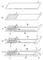
- FIG. 1 it is a perspective view which shows the manufacturing method of a film type thermistor sensor in order of a process.
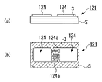
- Example of the metal nitride material for thermistors which concerns on this invention, its manufacturing method, and a film type thermistor sensor it is the front view and top view which show the element
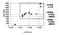
- it is a graph which shows the relationship between 25 degreeC resistivity and B constant.
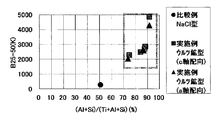
- it is a graph which shows the relationship between (Al + Si) / (Ti + Al + Si) ratio and B constant.
- Example which concerns on this invention it is a graph which shows the relationship between O / (O + N) ratio and N / (Ti + Al + Si + N) ratio.
- XRD X-ray diffraction
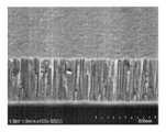
- it is a cross-sectional SEM photograph which shows an Example with strong c-axis orientation.
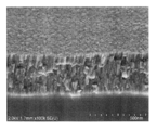
- it is a cross-sectional SEM photograph which shows an Example with a strong a-axis orientation.
- FIGS. 1 to 3 an embodiment of a metal nitride material for a thermistor according to the present invention, a manufacturing method thereof, and a film type thermistor sensor will be described with reference to FIGS. 1 to 3.
- the scale is appropriately changed as necessary to make each part recognizable or easily recognizable.
- the crystal structure is a single phase of a hexagonal wurtzite type (space group P6 3 mc (No. 186)).
- the crystal structure is a hexagonal wurtzite single phase.
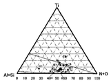
- the metal nitride material for the thermistor has a composition in a region surrounded by points A, B, C, and D in the ternary phase diagram of Ti- (Al + Si)-(N + O) system as shown in FIG. It is a metal nitride having a wurtzite type crystal phase.
- the wurtzite type crystal structure is the hexagonal space group P6 3 mc (No. 186), and Ti, Al, and Si belong to the same atomic site and are in a so-called solid solution state (for example, in the case of Ti 0.1 Al 0.88 Si 0.02 N, Ti, Al, and Si are present at the same atomic site with a probability of 10%, 88%, and 2%.)
- the wurtzite type has a (Ti, Al, Si) N4 tetrahedral apex connection structure, the nearest site of the (Ti, Al, Si) site is N (nitrogen), and (Ti, Al, Si) is Nitrogen tetracoordinate.
- V vanadium
- Cr chromium
- Mn manganese
- Fe iron
- Co cobalt
- the effective ionic radius is a physical property value often used for grasping the distance between atoms, and the literature value of Shannon's ionic radius, which is well known, is logically considered to be a wurtzite type V (Al , Si) N, Cr (Al, Si) N, Mn (Al, Si) N, Fe (Al, Si) N, and Co (Al, Si) N.
- Table 1 shows effective ionic radii of each ion species of Si, Al, Ti, V, Cr, Mn, Fe, and Co (reference paper RD Shannon, Acta Crystallogr., Sect. A, 32, 751). (1976)).
- the wurtzite type is tetracoordinate, and when the effective ionic radius of tetracoordinate with respect to M is seen, Co ⁇ Fe ⁇ Mn in the case of bivalent, Al ⁇ Fe in the case of trivalent, and tetravalent In this case, Si ⁇ Co, Mn ⁇ Cr ⁇ Ti, and in the case of pentavalent, Cr ⁇ V. From these results, it is considered that (Al, Si, Co) ⁇ Fe ⁇ Mn ⁇ Cr ⁇ (V, Ti) and Si ⁇ Co.
- the ionic radius is Al ⁇ Co ⁇ Fe ⁇ Mn ⁇ Cr ⁇ V ⁇ Ti. Recognize. (HS in Table 1 indicates a high spin state and LS indicates a low spin state.) From the above results, the ionic radius is (Al, Si) ⁇ Co ⁇ Fe ⁇ Mn ⁇ Cr ⁇ V ⁇ Ti. I understand that.
- the thermistor characteristics can be obtained by replacing the (Al, Si) site of the wurtzite type (Al, Si) N of the insulator with Ti or the like to carry out carrier doping and increase electrical conduction.
- Ti has a larger effective ionic radius than (Al, Si)
- the average ionic radius between (Al, Si) and Ti is To increase.
- the lattice constant increased is that the average ionic radius increased due to the increase in the (M + A) / (M + A + Al) ratio because the ionic radius of M such as Ti was larger than the ionic radius of Al. (Although the valence is different, from Table 1, it is unlikely that Al has a larger ionic radius than Si.
- the main factor for the increase in the lattice constant in this test is the effect of increasing the amount of M such as Ti. Conceivable.).
- the metal nitride material for a thermistor of this embodiment is a columnar crystal that is formed in a film shape and extends in a direction perpendicular to the surface of the film. Further, it is preferable that the c-axis is oriented more strongly than the a-axis in the direction perpendicular to the film surface. Whether the a-axis orientation (100) is strong or the c-axis orientation (002) is strong in the direction perpendicular to the film surface (film thickness direction) is determined using X-ray diffraction (XRD).
- XRD X-ray diffraction
- the orientation was investigated, and the peak intensity ratio of (100) (hkl index indicating a-axis orientation) and (002) (hkl index indicating c-axis orientation) was calculated as “(100) peak intensity” / “(002) When the “peak intensity of” is less than 1, the c-axis orientation is strong.
- the film type thermistor sensor 1 includes an insulating film 2, a thin film thermistor section 3 formed on the insulating film 2 from the metal nitride material for the thermistor, and at least the thin film thermistor section 3. And a pair of pattern electrodes 4 formed thereon.
- the insulating film 2 is formed in a band shape with, for example, a polyimide resin sheet.
- PET polyethylene terephthalate
- PEN polyethylene naphthalate, or the like may be used.
- the pair of pattern electrodes 4 is formed by patterning a laminated metal film of, for example, a Cr film and an Au film, and a pair of comb-shaped electrode portions 4a having a comb-shaped pattern arranged on the thin film thermistor portion 3 so as to face each other, and these comb-shaped electrodes A tip end portion is connected to the portion 4a, and a base end portion is disposed at an end portion of the insulating film 2 and has a pair of linear extending portions 4b extending.
- a plating portion 4c such as Au plating is formed as a lead wire drawing portion on the base end portion of the pair of linear extending portions 4b. One end of a lead wire is joined to the plating portion 4c with a solder material or the like.
- the polyimide coverlay film 5 is pressure-bonded on the insulating film 2 except for the end of the insulating film 2 including the plated portion 4c. In place of the polyimide coverlay film 5, a polyimide or epoxy resin material layer may be formed on the insulating film 2 by printing.
- the manufacturing method of the metal nitride material for the thermistors of this embodiment uses an M-Al-Si alloy sputtering target (where M represents at least one of Ti, V, Cr, Mn, Fe, and Co). And a film forming step of forming a film by performing reactive sputtering in an atmosphere containing nitrogen and oxygen. Moreover, it is preferable to set the sputtering gas pressure in the reactive sputtering to less than 0.67 Pa. Furthermore, it is preferable to irradiate the formed film with nitrogen plasma after the film formation step.
- M-Al-Si alloy sputtering target where M represents at least one of Ti, V, Cr, Mn, Fe, and Co.
- the present embodiment is formed on the insulating film 2 of a polyimide film having a thickness of 50 ⁇ m shown in FIG. 3A by reactive sputtering as shown in FIG.
- a thin film thermistor portion 3 made of the metal nitride material for thermistor is formed to a thickness of 200 nm.
- M Ti
- sputtering conditions at that time are, for example, ultimate vacuum: 5 ⁇ 10 ⁇ 6 Pa, sputtering gas pressure: 0.4 Pa, target input power (output): 300 W, Ar gas + nitrogen gas + oxygen In a gas mixed gas atmosphere, the nitrogen gas partial pressure is set to 19.8% and the oxygen gas partial pressure is set to 0.2%.
- the thin film thermistor portion 3 is formed by forming a metal nitride material for the thermistor into a desired size using a metal mask. Note that it is desirable to irradiate the formed thin film thermistor portion 3 with nitrogen plasma. For example, the thin film thermistor section 3 is irradiated with nitrogen plasma under a vacuum degree: 6.7 Pa, an output: 200 W, and an N 2 gas atmosphere.
- a Cr film is formed to 20 nm, and an Au film is further formed to 200 nm.
- prebaking is performed at 110 ° C. for 1 minute 30 seconds, and after exposure with an exposure apparatus, unnecessary portions are removed with a developer, and post baking is performed at 150 ° C. for 5 minutes. Patterning is performed at. Thereafter, unnecessary electrode portions are wet-etched with a commercially available Au etchant and Cr etchant, and as shown in FIG. 3C, pattern electrodes 4 having desired comb-shaped electrode portions 4a are formed by resist stripping. .
- the pattern electrode 4 may be formed on the insulating film 2 first, and the thin film thermistor portion 3 may be formed on the comb electrode portion 4a.
- the comb electrode portion 4 a of the pattern electrode 4 is formed under the thin film thermistor portion 3.
- a polyimide coverlay film 5 with an adhesive having a thickness of 50 ⁇ m is placed on the insulating film 2 and pressed by a press at 150 ° C. and 2 MPa for 10 minutes. Adhere. Further, as shown in FIG. 3E, an end portion of the linearly extending portion 4b is formed with a 2 ⁇ m Au thin film by using, for example, an Au plating solution to form a plated portion 4c.
- each film type thermistor sensor is formed from the large sheet. Cut to 1. In this way, for example, a thin film thermistor sensor 1 having a size of 25 ⁇ 3.6 mm and a thickness of 0.1 mm is obtained.
- the general formula: M x (Al 1-v Si v ) y (N 1-w O w ) z (where M is Ti, V, Cr, Mn , Fe and Co. 0.0 ⁇ v ⁇ 0.3, 0.70 ⁇ y / (x + y) ⁇ 0.98, 0.45 ⁇ z ⁇ 0.55, 0 ⁇ w ⁇ 0 .35, x + y + z 1), and its crystal structure is a single phase of a hexagonal wurtzite type (space group P63mc (No. 186)), so it is good without firing. A B constant is obtained and high heat resistance is obtained.
- the heat resistance is further improved due to the effect of oxygen filling nitrogen defects in the crystal.
- the metal nitride material for the thermistor is a columnar crystal extending in a direction perpendicular to the surface of the film, the film has high crystallinity and high heat resistance.
- a B constant higher than that when the a-axis orientation is strong can be obtained by orienting the c-axis more strongly than the a-axis in the direction perpendicular to the film surface.
- an M-Al-Si alloy sputtering target (wherein M represents at least one of Ti, V, Cr, Mn, Fe, and Co) is used. Since the film is formed by reactive sputtering in an atmosphere containing nitrogen and oxygen, the metal nitride material for the thermistor made of M x (Al, Si) y (N, O) z is formed without firing. Can do.
- the thin film thermistor portion 3 is formed on the insulating film 2 from the thermistor metal nitride material.
- the formed thin film thermistor portion 3 having a high B constant and high heat resistance allows the use of an insulating film 2 having low heat resistance such as a resin film, and a thin and flexible thermistor sensor having good thermistor characteristics. It is done.
- substrate materials using ceramics such as alumina are often used. For example, when the thickness is reduced to 0.1 mm, there is a problem that the substrate material is very brittle and easily broken. In this embodiment, a film is used. Therefore, for example, a very thin film type thermistor sensor having a thickness of 0.1 mm can be obtained.
- a film evaluation element 121 shown in FIG. 4 was produced as follows.
- M Ti, a metal nitride for thermistor where Ti x (Al, Si) y (N, O) z is used
- M Cr, Cr
- a material using a thermistor metal nitride x (Al, Si) y (N, O) z was prepared.
- a Ti—Al—Si alloy target and a Cr—Al—Si alloy target having various composition ratios are used to form a Si substrate S on a Si wafer with a thermal oxide film having a thickness of 500 nm.
- the thin film thermistor portion 3 of the metal nitride material for thermistor formed with various composition ratios shown in Table 2 was formed.
- the sputtering conditions at that time were as follows: ultimate vacuum: 5 ⁇ 10 ⁇ 6 Pa, sputtering gas pressure: 0.1-1 Pa, target input power (output): 100-500 W, mixed gas of Ar gas + nitrogen gas + oxygen gas In the atmosphere, the nitrogen gas partial pressure was changed to 10 to 100% and the oxygen gas partial pressure was changed to 0 to 3%.
- a 20 nm Cr film was formed on the thin film thermistor portion 3 by sputtering, and a 200 nm Au film was further formed. Further, after applying a resist solution thereon with a spin coater, pre-baking is performed at 110 ° C. for 1 minute 30 seconds. After exposure with an exposure apparatus, unnecessary portions are removed with a developing solution, and post baking is performed at 150 ° C. for 5 minutes. Then, patterning was performed. Thereafter, unnecessary electrode portions were wet-etched with a commercially available Au etchant and Cr etchant, and a patterned electrode 124 having a desired comb-shaped electrode portion 124a was formed by resist stripping.
- the X-ray source is MgK ⁇ (350 W)
- the path energy is 58.5 eV
- the measurement interval is 0.125 eV
- the photoelectron extraction angle with respect to the sample surface is 45 deg
- the analysis area is about Quantitative analysis was performed under the condition of 800 ⁇ m ⁇ .
- the quantitative accuracy the quantitative accuracy of N / (M + Al + Si + N + O) and O / (M + Al + Si + N + O) is ⁇ 2%
- the quantitative accuracy of (Al + Si) / (M + Al + Si) is ⁇ 1% (where M is Ti, V, Cr) , Mn, Fe and Co.)
- B constant (K) In (R25 / R50) / (1 / T25-1 / T50)
- T25 (K): 298.15K 25 ° C. is displayed as an absolute temperature
- T50 (K): 323.15K 50 ° C. is displayed as an absolute temperature
- FIG. 5 shows a graph showing the relationship between the resistivity at 25 ° C. and the B constant from the above results.
- the single phase of the mold can realize a high resistance and high B constant region having a specific resistance value at 25 ° C. of 100 ⁇ cm or more and a B constant of 1500 K or more.
- the B constant varies with the same (Al + Si) / (Ti + Al + Si) ratio because the nitrogen amount and oxygen amount in the crystal are different, or nitrogen defects, oxygen defects, etc. This is because the amount of lattice defects is different.
- Comparative Example 2 shown in Table 2 is a region of (Al + Si) / (Ti + Al + Si) ⁇ 0.7, and the crystal system is cubic NaCl type.
- the specific resistance value at 25 ° C. was less than 100 ⁇ cm
- the B constant was less than 1500 K
- the region was low resistance and low B constant.
- Comparative Example 1 shown in Table 2 is a region where (N + O) / (Ti + Al + Si + N + O) is less than 40%, and the metal is in a crystal state where nitriding is insufficient.
- Thin film X-ray diffraction (identification of crystal phase)
- the crystal phase of the thin film thermistor portion 3 obtained by the reactive sputtering method was identified by grazing incidence X-ray diffraction (Grazing Incidence X-ray Diffraction).
- all the examples of the present invention are films of wurtzite type phase, and since the orientation is strong, the a-axis orientation and the c-axis in the crystal axis in the direction perpendicular to the Si substrate S (film thickness direction). Which of the orientations is stronger was investigated using XRD. At this time, the peak intensity ratio of (100) (hkl index indicating a-axis orientation) and (002) (hkl index indicating c-axis orientation) was measured in order to investigate the orientation of crystal axes.
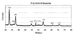
- FIG. 1 An example of an XRD profile of an example having a strong c-axis orientation is shown in FIG.
- (Al + Si) / (Ti + Al + Si) 0.88 (wurtzite hexagonal crystal), and the incident angle was 1 degree.
- the intensity of (002) is much stronger than (100).
- (*) is a peak derived from the apparatus and from the Si substrate with a thermal oxide film, and it is confirmed that it is not the peak of the sample body or the peak of the impurity phase. Moreover, the incident angle was set to 0 degree, the symmetry measurement was implemented, it confirmed that the peak had disappeared, and it was checked that it is a peak derived from a device and a Si substrate with a thermal oxide film.
- the correlation between the crystal structure and the electrical characteristics was further compared in detail for the example of the present invention which is a wurtzite type material.
- the example of the present invention which is a wurtzite type material.
- Table 2 with respect to those having a ratio of (Al + Si) / (Ti + Al + Si) close to the ratio, the material of the example in which the crystal axis having a strong degree of orientation in the direction perpendicular to the substrate surface is the c axis and the implementation having the a axis There are example materials.
- the material having a strong c-axis orientation has a slightly larger amount of nitrogen than the material having a strong a-axis orientation.
- the amount of O (O / (N + O)) it can be seen that the material having a strong a-axis orientation has a slightly larger oxygen content than the material having a strong c-axis orientation.
- the sample with less N / (Ti + Al + Si + N + O) has a larger amount of O / (N + O).
- the c-axis alignment material requires less oxygen.
- FIG. 10 shows a cross-sectional SEM photograph of the thin film thermistor portion 3 having high hexagonal crystal and c-axis orientation.
- the samples of these examples are obtained by cleaving and breaking the Si substrate S. Moreover, it is the photograph which observed the inclination at an angle of 45 degrees.
- the examples of the present invention are formed of dense columnar crystals. That is, it has been observed that columnar crystals grow in a direction perpendicular to the substrate surface. In addition, even when each film is formed with a thickness of 200 nm, 500 nm, and 1000 nm on the Si substrate S with a thermal oxide film, it is confirmed that the film is formed with dense columnar crystals as described above.
- the example with strong c-axis orientation in FIG. 10 had a particle size of about 10 nm ⁇ ( ⁇ 5 nm ⁇ ) and a length of about 520 nm. Further, in the example with a strong a-axis orientation in FIG.
- the particle size was about 10 nm ⁇ ( ⁇ 5 nm ⁇ ) and the length was about 510 nm.
- the particle diameter is the diameter of the columnar crystal in the substrate surface
- the length is the length (film thickness) of the columnar crystal in the direction perpendicular to the substrate surface.
- the aspect ratio of the columnar crystal is defined as (length) / (grain size)
- this embodiment has a large aspect ratio of 10 or more. It is considered that the film is dense due to the small grain size of the columnar crystals.
- even when each film is formed with a thickness of 200 nm, 500 nm, and 1000 nm on the Si substrate S with a thermal oxide film it is confirmed that the film is formed with dense columnar crystals as described above.
- the ionic radius of Ta is much larger than that of Ti, Al, and Si, and thus a wurtzite type phase cannot be produced in a high concentration Al region. Since the TaAlN system is not a wurtzite type phase, it is considered that the wurtzite type Ti- (Al + Si) -N system or Ti- (Al + Si)-(N + O) system has better heat resistance.
Landscapes
- Engineering & Computer Science (AREA)
- Microelectronics & Electronic Packaging (AREA)
- Physics & Mathematics (AREA)
- Electromagnetism (AREA)
- Manufacturing & Machinery (AREA)
- General Physics & Mathematics (AREA)
- Nonlinear Science (AREA)
- Thermistors And Varistors (AREA)
- Chemical & Material Sciences (AREA)
- Materials Engineering (AREA)
- Mechanical Engineering (AREA)
- Metallurgy (AREA)
- Organic Chemistry (AREA)
- Physical Vapour Deposition (AREA)
- Apparatuses And Processes For Manufacturing Resistors (AREA)
Abstract
Description
近年、樹脂フィルム上にサーミスタ材料を形成したフィルム型サーミスタセンサの開発が検討されており、フィルムに直接成膜できるサーミスタ材料の開発が望まれている。すなわち、フィルムを用いることで、フレキシブルなサーミスタセンサが得られることが期待される。さらに、0.1mm程度の厚さを持つ非常に薄いサーミスタセンサの開発が望まれているが、従来はアルミナ等のセラミックスを用いた基板材料がしばしば用いられ、例えば、厚さ0.1mmへと薄くすると非常に脆く壊れやすい等の問題があったが、フィルムを用いることで非常に薄いサーミスタセンサが得られることが期待される。
しかしながら、樹脂材料で構成されるフィルムは、一般的に耐熱温度が150℃以下と低く、比較的耐熱温度の高い材料として知られるポリイミドでも200℃程度の耐熱性しかないため、サーミスタ材料の形成工程において熱処理が加わる場合は、適用が困難であった。上記従来の酸化物サーミスタ材料では、所望のサーミスタ特性を実現するために550℃以上の焼成が必要であり、フィルムに直接成膜したフィルム型サーミスタセンサを実現できないという問題点があった。そのため、非焼成で直接成膜できるサーミスタ材料の開発が望まれているが、上記特許文献4に記載のサーミスタ材料でも、所望のサーミスタ特性を得るために、必要に応じて、得られた薄膜を350~600℃で熱処理する必要があった。また、このサーミスタ材料では、Ta−Al−N系材料の実施例において、B定数:500~3000K程度の材料が得られているが、耐熱性に関する記述がなく、窒化物系材料の熱的信頼性が不明であった。
また、特許文献5のCr−N−M系材料は、B定数が500以下と小さい材料であり、また、200℃以上1000℃以下の熱処理を実施しないと、200℃以内の耐熱性が確保できないことから、フィルムに直接成膜したフィルム型サーミスタセンサが実現できないという問題点があった。そのため、非焼成で直接成膜できるサーミスタ材料の開発が望まれている。
したがって、本発明は、上記知見から得られたものであり、前記課題を解決するために以下の構成を採用した。
このサーミスタ用金属窒化物材料では、一般式:Mx(Al1−vSiv)y(N1−wOw)z(但し、MはTi,V,Cr,Mn,Fe及びCoの少なくとも1種を示す。0.0<v<0.3、0.70≦y/(x+y)≦0.98、0.45≦z≦0.55、0<w≦0.35、x+y+z=1)で示される金属窒化物からなり、その結晶構造が、六方晶系のウルツ鉱型の単相であるので、非焼成で良好なB定数が得られると共に高い耐熱性を有している。特に、酸素(O)が含まれることで、結晶内の窒素欠陥を酸素が埋める、もしくは、格子間酸素が導入される等の効果によって耐熱性がより向上する。
また、上記「y/(x+y)」(すなわち、(Al+Si)/(M+Al+Si))が0.98を超えると、抵抗率が非常に高く、きわめて高い絶縁性を示すため、サーミスタ材料として適用できない。
また、上記「z」(すなわち、(N+O)/(M+Al+Si+N+O))が0.45未満であると、窒化量が少ないため、ウルツ鉱型の単相が得られず、十分な高抵抗と高B定数とが得られない。
さらに、上記「z」(すなわち、(N+O)/(M+Al+Si+N+O))が0.55を超えると、ウルツ鉱型の単相を得ることができない。このことは、ウルツ鉱型の単相において、窒素サイトにおける欠陥がない場合の化学量論比が0.5(すなわち、N/(M+Al+Si+N)=0.5)であることと、窒素サイトにおける欠陥を酸素が全て補った場合の化学量論比が0.5(すなわち、(N+O)/(M+Al+Si+N+O)=0.5)であることとに起因する。0.5を超えるz量については、格子間酸素が導入されたことと、XPS分析における軽元素(窒素、酸素)の定量精度とに起因するものである。
また、本研究において、上記「w」(すなわち、O/(N+O))が0.35を超えたウルツ鉱型の単相を得ることができなかった。このことは、w=1、かつ、y/(x+y)=0では、ルチル型(M1)O2相、コランダム型(M2)2O3相、スピネル型(M3)3O4相(但し、M1=Ti,M2=V,Cr,Fe,M3=Mn,Coを示す。)であり、w=1、かつ、y/(x+y)=1、かつ、V=0では、コランダム型Al2O3相であり、w=1、かつ、y/(x+y)=1、かつ、V=1では、ルチル型SiO2相であることを考慮すると理解できる。w値が増え、窒素量に対し酸素量が増えると、ウルツ鉱型単相が得ることが困難であることがわかり、本研究では、O/(N+O)=0.35まで、ウルツ鉱型単相が得られることを見出している。
さらに、上記「v」(すなわち、Si/(Al+Si))が0.3以上であると、ウルツ鉱型単相の結晶性の優れた膜を得ることができなかった。このことは、v=1、かつ、y/(x+y)=1、かつ、w=1では、フェナス石(Be2SiO4)型構造をもつSi3N4相であり、v=1、かつ、y/(x+y)=1、かつ、w=0では、クリストバル石型、トリジマイト型、石英型のSiO2相であることを考慮すると理解できる。
すなわち、このサーミスタ用金属窒化物材料では、膜の表面に対して垂直方向に延在している柱状結晶であるので、膜の結晶性が高く、高い耐熱性が得られる。
すなわち、このサーミスタ用金属窒化物材料では、膜の表面に対して垂直方向にa軸よりc軸が強く配向しているので、a軸配向が強い場合に比べて高いB定数が得られ、さらに耐熱性に対する信頼性も優れている。
すなわち、このフィルム型サーミスタセンサでは、絶縁性フィルム上に第1から第3のいずれかの発明のサーミスタ用金属窒化物材料で薄膜サーミスタ部が形成されているので、非焼成で形成され高B定数で耐熱性の高い薄膜サーミスタ部により、樹脂フィルム等の耐熱性の低い絶縁性フィルムを用いることができると共に、良好なサーミスタ特性を有した薄型でフレキシブルなサーミスタセンサが得られる。
また、従来、アルミナ等のセラミックスを用いた基板材料がしばしば用いられ、例えば、厚さ0.1mmへと薄くすると非常に脆く壊れやすい等の問題があったが、本発明においてはフィルムを用いることができるので、例えば、厚さ0.1mmの非常に薄いフィルム型サーミスタセンサを得ることができる。
すなわち、このサーミスタ用金属窒化物材料の製造方法では、M−Al−Si合金スパッタリングターゲットを用いて窒素及び酸素含有雰囲気中で反応性スパッタを行って成膜するので、上記Mx(Al1−vSiv)y(N1−wOw)zからなる本発明のサーミスタ用金属窒化物材料を非焼成で成膜することができる。
すなわち、このサーミスタ用金属窒化物材料の製造方法では、反応性スパッタにおけるスパッタガス圧を、0.67Pa未満に設定するので、膜の表面に対して垂直方向にa軸よりc軸が強く配向している第3の発明に係るサーミスタ用金属窒化物材料の膜を形成することができる。
すなわち、本発明に係るサーミスタ用金属窒化物材料によれば、一般式:Mx(Al1−vSiv)y(N1−wOw)z(但し、MはTi,V,Cr,Mn,Fe及びCoの少なくとも1種を示す。0.0<v<0.3、0.70≦y/(x+y)≦0.98、0.45≦z≦0.55、0<w≦0.35、x+y+z=1)で示される金属窒化物からなり、その結晶構造が、六方晶系のウルツ鉱型の単相であるので、非焼成で良好なB定数が得られると共に高い耐熱性を有している。また、本発明に係るサーミスタ用金属窒化物材料の製造方法によれば、M−Al−Si合金スパッタリングターゲット(但し、MはTi,V,Cr,Mn,Fe及びCoの少なくとも1種を示す。)を用いて窒素及び酸素含有雰囲気中で反応性スパッタを行って成膜するので、上記Mx(Al,Si)y(N,O)zからなる本発明のサーミスタ用金属窒化物材料を非焼成で成膜することができる。さらに、本発明に係るフィルム型サーミスタセンサによれば、絶縁性フィルム上に本発明のサーミスタ用金属窒化物材料で薄膜サーミスタ部が形成されているので、樹脂フィルム等の耐熱性の低い絶縁性フィルムを用いて良好なサーミスタ特性を有した薄型でフレキシブルなサーミスタセンサが得られる。さらに、基板材料が、薄くすると非常に脆く壊れやすいセラミックスでなく、樹脂フィルムであることから、厚さ0.1mmの非常に薄いフィルム型サーミスタセンサが得られる。
で示される金属窒化物からなり、その結晶構造が、六方晶系のウルツ鉱型(空間群P63mc(No.186))の単相である。
なお、上記点A,B,C,Dの各組成比(x、y、z)(atm%)は、A(x,y,z=13.5、31.5、55.0),B(x,y,z=0.9、44.1、55.0),C(x,y,z=1.1、53.9、45.0),D(x,y,z=16.5、38.5、45.0)である。
なお、Ti以外に、V(バナジウム)、Cr(クロム)、Mn(マンガン)、Fe(鉄)、Co(コバルト)が同様に上記結晶構造においてTiと同じ原子サイトに存在することができ、Mの元素となり得る。有効イオン半径は、原子間の距離を把握することによく使われる物性値であり、特によく知られているShannonのイオン半径の文献値を用いると、論理的にもウルツ鉱型のV(Al,Si)N,Cr(Al,Si)N,Mn(Al,Si)N,Fe(Al,Si)N,Co(Al,Si)Nが得られると推測できる。
以下の表1にSi,Al,Ti,V,Cr,Mn,Fe,Coの各イオン種における有効イオン半径を示す(参照論文R.D.Shannon,Acta Crystallogr.,Sect.A,32,751(1976))。

本発明は、絶縁体のウルツ鉱型(Al,Si)Nの(Al,Si)サイトをTi等に置き換えることにより、キャリアドーピングし、電気伝導が増加することで、サーミスタ特性が得られるものあるが、例えば(Al,Si)サイトをTiに置き換えた場合は、(Al,Si)よりTiの方が有効イオン半径が大きいので、その結果、(Al,Si)とTiとの平均イオン半径は増加する。その結果、原子間距離が増加し、格子定数が増加すると推測できる。
なお、ウルツ鉱型を維持するため、(Al,Si)サイトへのTi等Mの置換量には固溶限界があり、Ti/(Ti+Al+Si)が0.3程度よりも大きくなると(すなわち、(Al+Si)/(Ti+Al+Si)が0.7より小さくなると)、ウルツ鉱型よりもNaCl型の方が生成されやすくなる。
なお、膜の表面に対して垂直方向(膜厚方向)にa軸配向(100)が強いかc軸配向(002)が強いかの判断は、X線回折(XRD)を用いて結晶軸の配向性を調べ、(100)(a軸配向を示すhkl指数)と(002)(c軸配向を示すhkl指数)とのピーク強度比から、「(100)のピーク強度」/「(002)のピーク強度」が1未満である場合、c軸配向が強いものとする。
上記一対のパターン電極4は、例えばCr膜とAu膜との積層金属膜でパターン形成され、薄膜サーミスタ部3上で互いに対向状態に配した櫛形パターンの一対の櫛形電極部4aと、これら櫛形電極部4aに先端部が接続され基端部が絶縁性フィルム2の端部に配されて延在した一対の直線延在部4bとを有している。
また、上記反応性スパッタにおけるスパッタガス圧を、0.67Pa未満に設定することが好ましい。
さらに、上記成膜工程後に、形成された膜に窒素プラズマを照射することが好ましい。
M=Tiとした場合、その時のスパッタ条件は、例えば到達真空度:5×10⁻⁶Pa、スパッタガス圧:0.4Pa、ターゲット投入電力(出力):300Wで、Arガス+窒素ガス+酸素ガスの混合ガス雰囲気下において窒素ガス分圧:19.8%、酸素ガス分圧:0.2%とする。また、メタルマスクを用いて所望のサイズにサーミスタ用金属窒化物材料を成膜して薄膜サーミスタ部3を形成する。なお、形成された薄膜サーミスタ部3に窒素プラズマを照射することが望ましい。例えば、真空度:6.7Pa、出力:200W及びN2ガス雰囲気下で、窒素プラズマを薄膜サーミスタ部3に照射させる。
このようにして、例えばサイズを25×3.6mmとし、厚さを0.1mmとした薄いフィルム型サーミスタセンサ1が得られる。
また、このサーミスタ用金属窒化物材料では、膜の表面に対して垂直方向に延在している柱状結晶であるので、膜の結晶性が高く、高い耐熱性が得られる。
さらに、このサーミスタ用金属窒化物材料では、膜の表面に対して垂直方向にa軸よりc軸を強く配向させることで、a軸配向が強い場合に比べて高いB定数が得られる。
また、従来、アルミナ等のセラミックスを用いた基板材料がしばしば用いられ、例えば、厚さ0.1mmへと薄くすると非常に脆く壊れやすい等の問題があったが、本実施形態においてはフィルムを用いることができるので、例えば、厚さ0.1mmの非常に薄いフィルム型サーミスタセンサを得ることができる。
本発明の実施例及び比較例として、図4に示す膜評価用素子121を次のように作製した。なお、以下の本発明の各実施例では、M=Tiとし、Tix(Al,Si)y(N,O)zであるサーミスタ用金属窒化物を用いたものと、M=Crとし、Crx(Al,Si)y(N,O)zであるサーミスタ用金属窒化物を用いたものとを作製した。
まず、反応性スパッタ法にて、様々な組成比のTi−Al−Si合金ターゲット、Cr−Al−Si合金ターゲットを用いて、Si基板Sとなる熱酸化膜付きSiウエハ上に、厚さ500nmの表2に示す様々な組成比で形成されたサーミスタ用金属窒化物材料の薄膜サーミスタ部3を形成した。その時のスパッタ条件は、到達真空度:5×10⁻⁶Pa、スパッタガス圧:0.1~1Pa、ターゲット投入電力(出力):100~500Wで、Arガス+窒素ガス+酸素ガスの混合ガス雰囲気下において、窒素ガス分圧を10~100%、酸素ガス分圧を0~3%と変えて作製した。
なお、比較としてTix(Al,Si)y(N,O)zの組成比が本発明の範囲外であって結晶系が異なる比較例についても同様に作製して評価を行った。
(1)組成分析
反応性スパッタ法にて得られた薄膜サーミスタ部3について、X線光電子分光法(XPS)にて元素分析を行った。このXPSでは、Arスパッタにより、最表面から深さ20nmのスパッタ面において、定量分析を実施した。その結果を表2に示す。なお、以下の表中の組成比は「原子%」で示している。一部のサンプルに対して、最表面から深さ100nmのスパッタ面における定量分析を実施し、深さ20nmのスパッタ面と定量精度の範囲内で同じ組成であることを確認している。
反応性スパッタ法にて得られた薄膜サーミスタ部3について、4端子法にて25℃での比抵抗を測定した。その結果を表2及び表3に示す。
(3)B定数測定
膜評価用素子121の25℃及び50℃の抵抗値を恒温槽内で測定し、25℃と50℃との抵抗値よりB定数を算出した。その結果を表2及び表3に示す。また、25℃と50℃との抵抗値より負の温度特性をもつサーミスタであることを確認している。
B定数(K)=In(R25/R50)/(1/T25−1/T50)
R25(Ω):25℃における抵抗値
R50(Ω):50℃における抵抗値
T25(K):298.15K 25℃を絶対温度表示
T50(K):323.15K 50℃を絶対温度表示
表2に示す比較例1は、(N+O)/(Ti+Al+Si+N+O)が40%に満たない領域であり、金属が窒化不足の結晶状態になっている。この比較例1は、NaCl型でも、ウルツ鉱型でもない、非常に結晶性の劣る状態であった。また、これら比較例では、B定数及び抵抗値が共に非常に小さく、金属的振舞いに近いことがわかった。
なお、M=Crの場合である表3に示す実施例でも、Al/(Cr+Al+Si)=0.7~0.98,(N+O)/(Cr+Al+Si+N+O)=0.45~0.55とすることで、ウルツ鉱型六方晶が得られ、高抵抗かつ高B定数のサーミスタ特性が得られている。
反応性スパッタ法にて得られた薄膜サーミスタ部3を、視斜角入射X線回折(Grazing Incidence X−ray Diffraction)により、結晶相を同定した。この薄膜X線回折は、微小角X線回折実験であり、管球をCuとし、入射角を1度とすると共に2θ=20~130度の範囲で測定した。一部のサンプルについては、入射角を0度とし、2θ=20~100度の範囲で測定した。
なお、M=Crの場合においても、(Al+Si)/(Cr+Al+Si)≧0.7の領域においては、ウルツ鉱型相であることを確認した。
なお、表2に示す比較例1は、上述したように結晶相がウルツ鉱型相でもNaCl型相でもなく、本試験においては同定できなかった。また、これらの比較例は、XRDのピーク幅が非常に広いことから、非常に結晶性の劣る材料であった。これは、電気特性により金属的振舞いに近いことから、窒化不足、かつ、酸化不足の金属相になっていると考えられる。


a軸配向が強い実施例のXRDプロファイルの一例を、図9に示す。この実施例は、(Al+Si)/(Ti+Al+Si)=0.87(ウルツ鉱型六方晶)であり、入射角を1度として測定した。この結果からわかるように、この実施例では、(002)よりも(100)の強度が非常に強くなっている。
なお、グラフ中(*)は装置由来および熱酸化膜付きSi基板由来のピークであり、サンプル本体のピーク、もしくは、不純物相のピークではないことを確認している。また、入射角を0度として、対称測定を実施し、そのピークが消失していることを確認し、装置由来および熱酸化膜付きSi基板由来のピークであることを確認した。
表2に示すように、(Al+Si)/(Ti+Al+Si)比が近い比率のものに対し、基板面に垂直方向の配向度の強い結晶軸がc軸である実施例の材料とa軸である実施例の材料とがある。
これら両者を比較すると、(Al+Si)/(Ti+Al+Si)比がほぼ同じであると、a軸配向が強い材料よりもc軸配向が強い材料の方が、B定数が大きいことがわかる。
また、(Al+Si)/(Ti+Al+Si)比とSi/(Al+Si)比との双方が近い比率のものに対し、基板面に垂直方向の配向度の強い結晶軸がc軸である実施例の材料とa軸である実施例の材料とがある。これら両者を比較した場合においても、Si/(Al+Si)比が同じであると、a軸配向が強い材料よりもc軸配向が強い材料の方が、B定数が大きいことがわかる。
次に、薄膜サーミスタ部3の断面における結晶形態を示す一例として、熱酸化膜付きSi基板S上に520nm程度成膜された実施例((Al+Si)/(Ti+Al+Si)=0.88,ウルツ鉱型六方晶、c軸配向性が強い)の薄膜サーミスタ部3における断面SEM写真を、図10に示す。また、別の実施例((Al+Si)/(Ti+Al+Si)=0.87,ウルツ鉱型六方晶、a軸配向性が強い)の薄膜サーミスタ部3における断面SEM写真を、図11に示す。
これらの実施例のサンプルは、Si基板Sをへき開破断したものを用いている。また、45°の角度で傾斜観察した写真である。
なお、図中の柱状結晶サイズについて、図10のc軸配向が強い実施例は、粒径が10nmφ(±5nmφ)、長さ520nm程度であった。また、図11のa軸配向が強い実施例は、粒径が10nmφ(±5nmφ)、長さ510nm程度であった。なお、ここでの粒径は、基板面内における柱状結晶の直径であり、長さは、基板面に垂直な方向の柱状結晶の長さ(膜厚)である。
柱状結晶のアスペクト比を(長さ)÷(粒径)として定義すると、本実施例は10以上の大きいアスペクト比をもっている。柱状結晶の粒径が小さいことにより、膜が緻密となっていると考えられる。なお、熱酸化膜付きSi基板S上に200nm、500nm、1000nmの厚さでそれぞれ成膜された場合にも、上記同様、緻密な柱状結晶で形成されていることを確認している。
表2に示す実施例及び比較例の一部において、大気中,125℃,1000hの耐熱試験前後における抵抗値及びB定数を評価した。その結果を表4に示す。なお、比較として従来のTa−Al−N系材料による比較例も同様に評価した。また、参考として、酸素ガスを含有しない窒素ガスとArガスとの混合ガス雰囲気中で反応性スパッタを行い、Ti−(Al+Si)−N系材料による薄膜サーミスタ部3を形成した参考例1(ウルツ鉱型六方晶、c軸配向が強い)についても同様に耐熱試験を行った結果を、表4に併せて示す。
また、酸素を積極的に含有させていないTi−(Al+Si)−N系材料による参考例1は、比較例よりも耐熱性に優れているが、この参考例1に比べて、酸素を積極的に含有させた本発明のTi−(Al+Si)−(N+O)系材料による実施例の方が、抵抗値上昇率が小さく、さらに耐熱性に優れていることがわかる。

例えば、上記実施例では、M=Ti又はCrとしてM−(Al+Si)−(N+O)のサーミスタ用金属窒化物材料を作製したが、V,Mn,Fe,Coの少なくとも1種をTi又はCrの少なくとも一部に対して置換可能であり、同様の特性を得ることができる。
Claims (6)
- サーミスタに用いられる金属窒化物材料であって、
一般式:Mx(Al1−vSiv)y(N1−wOw)z(但し、MはTi,V,Cr,Mn,Fe及びCoの少なくとも1種を示す。0.0<v<0.3、0.70≦y/(x+y)≦0.98、0.45≦z≦0.55、0<w≦0.35、x+y+z=1)で示される金属窒化物からなり、
その結晶構造が、六方晶系のウルツ鉱型の単相であることを特徴とするサーミスタ用金属窒化物材料。 - 請求項1に記載のサーミスタ用金属窒化物材料において、
膜状に形成され、
前記膜の表面に対して垂直方向に延在している柱状結晶であることを特徴とするサーミスタ用金属窒化物材料。 - 請求項1又は2に記載のサーミスタ用金属窒化物材料において、
膜状に形成され、
前記膜の表面に対して垂直方向にa軸よりc軸が強く配向していることを特徴とするサーミスタ用金属窒化物材料。 - 絶縁性フィルムと、
該絶縁性フィルム上に請求項1から3のいずれか一項に記載のサーミスタ用金属窒化物材料で形成された薄膜サーミスタ部と、
少なくとも前記薄膜サーミスタ部の上又は下に形成された一対のパターン電極とを備えていることを特徴とするフィルム型サーミスタセンサ。 - 請求項1から3のいずれか一項に記載のサーミスタ用金属窒化物材料を製造する方法であって、
M−Al−Si合金スパッタリングターゲット(但し、MはTi,V,Cr,Mn,Fe及びCoの少なくとも1種を示す。)を用いて窒素及び酸素含有雰囲気中で反応性スパッタを行って成膜する成膜工程を有していることを特徴とするサーミスタ用金属窒化物材料の製造方法。 - 請求項5に記載のサーミスタ用金属窒化物材料の製造方法において、
前記反応性スパッタにおけるスパッタガス圧を、0.67Pa未満に設定することを特徴とするサーミスタ用金属窒化物材料の製造方法。
Priority Applications (3)
| Application Number | Priority Date | Filing Date | Title |
|---|---|---|---|
| US14/915,399 US10304597B2 (en) | 2013-08-30 | 2014-08-15 | Metal nitride material for thermistor, method for producing same, and film type thermistor sensor |
| CN201480031428.0A CN105264619B (zh) | 2013-08-30 | 2014-08-15 | 热敏电阻用金属氮化物材料及其制造方法以及薄膜型热敏电阻传感器 |
| KR1020167001545A KR20160048761A (ko) | 2013-08-30 | 2014-08-15 | 서미스터용 금속 질화물 재료 및 그 제조 방법 그리고 필름형 서미스터 센서 |
Applications Claiming Priority (2)
| Application Number | Priority Date | Filing Date | Title |
|---|---|---|---|
| JP2013180303 | 2013-08-30 | ||
| JP2013-180303 | 2013-08-30 |
Publications (1)
| Publication Number | Publication Date |
|---|---|
| WO2015029915A1 true WO2015029915A1 (ja) | 2015-03-05 |
Family
ID=52586473
Family Applications (1)
| Application Number | Title | Priority Date | Filing Date |
|---|---|---|---|
| PCT/JP2014/072077 Ceased WO2015029915A1 (ja) | 2013-08-30 | 2014-08-15 | サーミスタ用金属窒化物材料及びその製造方法並びにフィルム型サーミスタセンサ |
Country Status (6)
| Country | Link |
|---|---|
| US (1) | US10304597B2 (ja) |
| JP (1) | JP6355022B2 (ja) |
| KR (1) | KR20160048761A (ja) |
| CN (1) | CN105264619B (ja) |
| TW (1) | TW201515027A (ja) |
| WO (1) | WO2015029915A1 (ja) |
Cited By (1)
| Publication number | Priority date | Publication date | Assignee | Title |
|---|---|---|---|---|
| CN111549322A (zh) * | 2020-06-18 | 2020-08-18 | 天津职业技术师范大学(中国职业培训指导教师进修中心) | 一种AlCrTiSiN/AlCrTiSiON多层复合涂层及其制备工艺 |
Families Citing this family (2)
| Publication number | Priority date | Publication date | Assignee | Title |
|---|---|---|---|---|
| JP6308436B2 (ja) * | 2013-07-25 | 2018-04-11 | 三菱マテリアル株式会社 | サーミスタ用金属窒化物材料及びその製造方法並びにフィルム型サーミスタセンサ |
| CN111826621A (zh) * | 2019-04-17 | 2020-10-27 | 中国兵器工业第五九研究所 | 玻璃模压模具涂层及其制备方法和应用 |
Citations (10)
| Publication number | Priority date | Publication date | Assignee | Title |
|---|---|---|---|---|
| JPH0453202A (ja) * | 1990-06-20 | 1992-02-20 | Oki Electric Ind Co Ltd | 発熱抵抗体 |
| JPH10270201A (ja) | 1997-03-21 | 1998-10-09 | Res Inst Electric Magnetic Alloys | Cr−N基歪抵抗膜およびその製造法ならびに歪センサ |
| JP2000068110A (ja) | 1998-08-19 | 2000-03-03 | Tdk Corp | サーミスタ用組成物 |
| JP2000348903A (ja) | 1999-06-03 | 2000-12-15 | Matsushita Electric Ind Co Ltd | 薄膜サーミスタ素子および薄膜サーミスタ素子の製造方法 |
| JP2004303804A (ja) * | 2003-03-28 | 2004-10-28 | Susumu Co Ltd | 3元合金材料 |
| JP2004319737A (ja) | 2003-04-16 | 2004-11-11 | Osaka Prefecture | サーミスタ用材料及びその製造方法 |
| JP2006324520A (ja) | 2005-05-19 | 2006-11-30 | Mitsubishi Materials Corp | サーミスタ薄膜及びその製造方法 |
| JP2009259911A (ja) * | 2008-04-14 | 2009-11-05 | Toyota Central R&D Labs Inc | 水素雰囲気用サーミスタ材料 |
| JP2012036506A (ja) * | 2011-11-08 | 2012-02-23 | Tungaloy Corp | 被覆部材 |
| JP2012061539A (ja) * | 2010-09-15 | 2012-03-29 | Mitsubishi Materials Corp | 仕上げ面粗さに優れたcbnインサート |
Family Cites Families (8)
| Publication number | Priority date | Publication date | Assignee | Title |
|---|---|---|---|---|
| JPH0453502A (ja) * | 1990-06-20 | 1992-02-21 | Seiko Instr Inc | クロム拡散合金化処理を施したステンレス鋼製時計バンドの製造方法 |
| US6299294B1 (en) * | 1999-07-29 | 2001-10-09 | Hewlett-Packard Company | High efficiency printhead containing a novel oxynitride-based resistor system |
| JP2001230060A (ja) * | 2000-02-21 | 2001-08-24 | Tdk Corp | 抵抗素子 |
| US7473031B2 (en) * | 2002-04-01 | 2009-01-06 | Palo Alto Research Center, Incorporated | Resistive thermal sensing |
| WO2008133345A1 (en) * | 2007-04-25 | 2008-11-06 | Canon Kabushiki Kaisha | Oxynitride semiconductor |
| JP5451280B2 (ja) * | 2008-10-09 | 2014-03-26 | キヤノン株式会社 | ウルツ鉱型結晶成長用基板およびその製造方法ならびに半導体装置 |
| JP5477670B2 (ja) * | 2012-02-28 | 2014-04-23 | 三菱マテリアル株式会社 | サーミスタ用金属窒化物材料及びその製造方法並びにフィルム型サーミスタセンサ |
| CN102731108B (zh) * | 2012-07-19 | 2013-11-27 | 中国科学院新疆理化技术研究所 | 一种高b值负温度系数热敏电阻材料的制备方法 |
-
2014
- 2014-07-30 JP JP2014154640A patent/JP6355022B2/ja not_active Expired - Fee Related
- 2014-08-15 CN CN201480031428.0A patent/CN105264619B/zh not_active Expired - Fee Related
- 2014-08-15 US US14/915,399 patent/US10304597B2/en active Active
- 2014-08-15 WO PCT/JP2014/072077 patent/WO2015029915A1/ja not_active Ceased
- 2014-08-15 KR KR1020167001545A patent/KR20160048761A/ko not_active Withdrawn
- 2014-08-21 TW TW103128794A patent/TW201515027A/zh unknown
Patent Citations (10)
| Publication number | Priority date | Publication date | Assignee | Title |
|---|---|---|---|---|
| JPH0453202A (ja) * | 1990-06-20 | 1992-02-20 | Oki Electric Ind Co Ltd | 発熱抵抗体 |
| JPH10270201A (ja) | 1997-03-21 | 1998-10-09 | Res Inst Electric Magnetic Alloys | Cr−N基歪抵抗膜およびその製造法ならびに歪センサ |
| JP2000068110A (ja) | 1998-08-19 | 2000-03-03 | Tdk Corp | サーミスタ用組成物 |
| JP2000348903A (ja) | 1999-06-03 | 2000-12-15 | Matsushita Electric Ind Co Ltd | 薄膜サーミスタ素子および薄膜サーミスタ素子の製造方法 |
| JP2004303804A (ja) * | 2003-03-28 | 2004-10-28 | Susumu Co Ltd | 3元合金材料 |
| JP2004319737A (ja) | 2003-04-16 | 2004-11-11 | Osaka Prefecture | サーミスタ用材料及びその製造方法 |
| JP2006324520A (ja) | 2005-05-19 | 2006-11-30 | Mitsubishi Materials Corp | サーミスタ薄膜及びその製造方法 |
| JP2009259911A (ja) * | 2008-04-14 | 2009-11-05 | Toyota Central R&D Labs Inc | 水素雰囲気用サーミスタ材料 |
| JP2012061539A (ja) * | 2010-09-15 | 2012-03-29 | Mitsubishi Materials Corp | 仕上げ面粗さに優れたcbnインサート |
| JP2012036506A (ja) * | 2011-11-08 | 2012-02-23 | Tungaloy Corp | 被覆部材 |
Cited By (2)
| Publication number | Priority date | Publication date | Assignee | Title |
|---|---|---|---|---|
| CN111549322A (zh) * | 2020-06-18 | 2020-08-18 | 天津职业技术师范大学(中国职业培训指导教师进修中心) | 一种AlCrTiSiN/AlCrTiSiON多层复合涂层及其制备工艺 |
| CN111549322B (zh) * | 2020-06-18 | 2022-08-05 | 天津职业技术师范大学(中国职业培训指导教师进修中心) | 一种AlCrTiSiN/AlCrTiSiON多层复合涂层及其制备工艺 |
Also Published As
| Publication number | Publication date |
|---|---|
| US20160223407A1 (en) | 2016-08-04 |
| US10304597B2 (en) | 2019-05-28 |
| JP2015065418A (ja) | 2015-04-09 |
| CN105264619A (zh) | 2016-01-20 |
| KR20160048761A (ko) | 2016-05-04 |
| JP6355022B2 (ja) | 2018-07-11 |
| TW201515027A (zh) | 2015-04-16 |
| CN105264619B (zh) | 2018-02-13 |
Similar Documents
| Publication | Publication Date | Title |
|---|---|---|
| JP6354947B2 (ja) | サーミスタ用金属窒化物材料及びその製造方法並びにフィルム型サーミスタセンサ | |
| JP6318915B2 (ja) | サーミスタ用金属窒化物材料及びその製造方法並びにフィルム型サーミスタセンサ | |
| JP6311879B2 (ja) | サーミスタ用金属窒化物材料及びその製造方法並びにフィルム型サーミスタセンサ | |
| JP6318916B2 (ja) | サーミスタ用金属窒化物材料及びその製造方法並びにフィルム型サーミスタセンサ | |
| JP6308435B2 (ja) | サーミスタ用金属窒化物材料及びその製造方法並びにフィルム型サーミスタセンサ | |
| JP6311878B2 (ja) | サーミスタ用金属窒化物材料及びその製造方法並びにフィルム型サーミスタセンサ | |
| JP6015426B2 (ja) | サーミスタ用金属窒化物材料及びその製造方法並びにフィルム型サーミスタセンサ | |
| WO2014097891A1 (ja) | サーミスタ用金属窒化物材料及びその製造方法並びにフィルム型サーミスタセンサ | |
| JP6120250B2 (ja) | サーミスタ用金属窒化物材料及びその製造方法並びにフィルム型サーミスタセンサ | |
| JP6308436B2 (ja) | サーミスタ用金属窒化物材料及びその製造方法並びにフィルム型サーミスタセンサ | |
| JP6120251B2 (ja) | サーミスタ用金属窒化物材料及びその製造方法並びにフィルム型サーミスタセンサ | |
| JP6015424B2 (ja) | サーミスタ用金属窒化物材料及びその製造方法並びにフィルム型サーミスタセンサ | |
| JP6355022B2 (ja) | サーミスタ用金属窒化物材料及びその製造方法並びにフィルム型サーミスタセンサ | |
| JP6308365B2 (ja) | サーミスタ用金属窒化物材料及びその製造方法並びにフィルム型サーミスタセンサ | |
| JP6115823B2 (ja) | サーミスタ用金属窒化物材料及びその製造方法並びにフィルム型サーミスタセンサ | |
| JP6308364B2 (ja) | サーミスタ用金属窒化物材料及びその製造方法並びにフィルム型サーミスタセンサ | |
| JP2016134505A (ja) | サーミスタ用金属窒化物材料及びその製造方法並びにフィルム型サーミスタセンサ | |
| JP6601614B2 (ja) | サーミスタ用金属窒化物材料及びその製造方法並びにフィルム型サーミスタセンサ | |
| JP2016134491A (ja) | サーミスタ用金属窒化物材料及びその製造方法並びにフィルム型サーミスタセンサ | |
| JP2016134490A (ja) | サーミスタ用金属窒化物材料及びその製造方法並びにフィルム型サーミスタセンサ | |
| JP2016134504A (ja) | サーミスタ用金属窒化物材料及びその製造方法並びにフィルム型サーミスタセンサ |
Legal Events
| Date | Code | Title | Description |
|---|---|---|---|
| WWE | Wipo information: entry into national phase |
Ref document number: 201480031428.0 Country of ref document: CN |
|
| 121 | Ep: the epo has been informed by wipo that ep was designated in this application |
Ref document number: 14839254 Country of ref document: EP Kind code of ref document: A1 |
|
| ENP | Entry into the national phase |
Ref document number: 20167001545 Country of ref document: KR Kind code of ref document: A |
|
| WWE | Wipo information: entry into national phase |
Ref document number: 2014839254 Country of ref document: EP |
|
| NENP | Non-entry into the national phase |
Ref country code: DE |
|
| WWE | Wipo information: entry into national phase |
Ref document number: 14915399 Country of ref document: US |