WO2015025692A1 - 素子製造方法および素子製造装置 - Google Patents
素子製造方法および素子製造装置 Download PDFInfo
- Publication number
- WO2015025692A1 WO2015025692A1 PCT/JP2014/070238 JP2014070238W WO2015025692A1 WO 2015025692 A1 WO2015025692 A1 WO 2015025692A1 JP 2014070238 W JP2014070238 W JP 2014070238W WO 2015025692 A1 WO2015025692 A1 WO 2015025692A1
- Authority
- WO
- WIPO (PCT)
- Prior art keywords
- intermediate product
- lid member
- pair
- organic semiconductor
- film
- Prior art date
- Legal status (The legal status is an assumption and is not a legal conclusion. Google has not performed a legal analysis and makes no representation as to the accuracy of the status listed.)
- Ceased
Links
Images


Classifications
-
- B—PERFORMING OPERATIONS; TRANSPORTING
- B23—MACHINE TOOLS; METAL-WORKING NOT OTHERWISE PROVIDED FOR
- B23K—SOLDERING OR UNSOLDERING; WELDING; CLADDING OR PLATING BY SOLDERING OR WELDING; CUTTING BY APPLYING HEAT LOCALLY, e.g. FLAME CUTTING; WORKING BY LASER BEAM
- B23K26/00—Working by laser beam, e.g. welding, cutting or boring
- B23K26/009—Working by laser beam, e.g. welding, cutting or boring using a non-absorbing, e.g. transparent, reflective or refractive, layer on the workpiece
-
- B—PERFORMING OPERATIONS; TRANSPORTING
- B23—MACHINE TOOLS; METAL-WORKING NOT OTHERWISE PROVIDED FOR
- B23K—SOLDERING OR UNSOLDERING; WELDING; CLADDING OR PLATING BY SOLDERING OR WELDING; CUTTING BY APPLYING HEAT LOCALLY, e.g. FLAME CUTTING; WORKING BY LASER BEAM
- B23K26/00—Working by laser beam, e.g. welding, cutting or boring
- B23K26/0006—Working by laser beam, e.g. welding, cutting or boring taking account of the properties of the material involved
-
- B—PERFORMING OPERATIONS; TRANSPORTING
- B23—MACHINE TOOLS; METAL-WORKING NOT OTHERWISE PROVIDED FOR
- B23K—SOLDERING OR UNSOLDERING; WELDING; CLADDING OR PLATING BY SOLDERING OR WELDING; CUTTING BY APPLYING HEAT LOCALLY, e.g. FLAME CUTTING; WORKING BY LASER BEAM
- B23K26/00—Working by laser beam, e.g. welding, cutting or boring
- B23K26/0093—Working by laser beam, e.g. welding, cutting or boring combined with mechanical machining or metal-working covered by other subclasses than B23K
-
- B—PERFORMING OPERATIONS; TRANSPORTING
- B23—MACHINE TOOLS; METAL-WORKING NOT OTHERWISE PROVIDED FOR
- B23K—SOLDERING OR UNSOLDERING; WELDING; CLADDING OR PLATING BY SOLDERING OR WELDING; CUTTING BY APPLYING HEAT LOCALLY, e.g. FLAME CUTTING; WORKING BY LASER BEAM
- B23K26/00—Working by laser beam, e.g. welding, cutting or boring
- B23K26/18—Working by laser beam, e.g. welding, cutting or boring using absorbing layers on the workpiece, e.g. for marking or protecting purposes
-
- B—PERFORMING OPERATIONS; TRANSPORTING
- B23—MACHINE TOOLS; METAL-WORKING NOT OTHERWISE PROVIDED FOR
- B23K—SOLDERING OR UNSOLDERING; WELDING; CLADDING OR PLATING BY SOLDERING OR WELDING; CUTTING BY APPLYING HEAT LOCALLY, e.g. FLAME CUTTING; WORKING BY LASER BEAM
- B23K26/00—Working by laser beam, e.g. welding, cutting or boring
- B23K26/20—Bonding
- B23K26/206—Laser sealing
-
- B—PERFORMING OPERATIONS; TRANSPORTING
- B23—MACHINE TOOLS; METAL-WORKING NOT OTHERWISE PROVIDED FOR
- B23K—SOLDERING OR UNSOLDERING; WELDING; CLADDING OR PLATING BY SOLDERING OR WELDING; CUTTING BY APPLYING HEAT LOCALLY, e.g. FLAME CUTTING; WORKING BY LASER BEAM
- B23K26/00—Working by laser beam, e.g. welding, cutting or boring
- B23K26/36—Removing material
- B23K26/361—Removing material for deburring or mechanical trimming
-
- B—PERFORMING OPERATIONS; TRANSPORTING
- B23—MACHINE TOOLS; METAL-WORKING NOT OTHERWISE PROVIDED FOR
- B23K—SOLDERING OR UNSOLDERING; WELDING; CLADDING OR PLATING BY SOLDERING OR WELDING; CUTTING BY APPLYING HEAT LOCALLY, e.g. FLAME CUTTING; WORKING BY LASER BEAM
- B23K26/00—Working by laser beam, e.g. welding, cutting or boring
- B23K26/36—Removing material
- B23K26/40—Removing material taking account of the properties of the material involved
- B23K26/402—Removing material taking account of the properties of the material involved involving non-metallic material, e.g. isolators
-
- H—ELECTRICITY
- H10—SEMICONDUCTOR DEVICES; ELECTRIC SOLID-STATE DEVICES NOT OTHERWISE PROVIDED FOR
- H10K—ORGANIC ELECTRIC SOLID-STATE DEVICES
- H10K50/00—Organic light-emitting devices
-
- H—ELECTRICITY
- H10—SEMICONDUCTOR DEVICES; ELECTRIC SOLID-STATE DEVICES NOT OTHERWISE PROVIDED FOR
- H10K—ORGANIC ELECTRIC SOLID-STATE DEVICES
- H10K71/00—Manufacture or treatment specially adapted for the organic devices covered by this subclass
- H10K71/10—Deposition of organic active material
- H10K71/18—Deposition of organic active material using non-liquid printing techniques, e.g. thermal transfer printing from a donor sheet
-
- B—PERFORMING OPERATIONS; TRANSPORTING
- B23—MACHINE TOOLS; METAL-WORKING NOT OTHERWISE PROVIDED FOR
- B23K—SOLDERING OR UNSOLDERING; WELDING; CLADDING OR PLATING BY SOLDERING OR WELDING; CUTTING BY APPLYING HEAT LOCALLY, e.g. FLAME CUTTING; WORKING BY LASER BEAM
- B23K2101/00—Articles made by soldering, welding or cutting
- B23K2101/36—Electric or electronic devices
- B23K2101/42—Printed circuits
-
- B—PERFORMING OPERATIONS; TRANSPORTING
- B23—MACHINE TOOLS; METAL-WORKING NOT OTHERWISE PROVIDED FOR
- B23K—SOLDERING OR UNSOLDERING; WELDING; CLADDING OR PLATING BY SOLDERING OR WELDING; CUTTING BY APPLYING HEAT LOCALLY, e.g. FLAME CUTTING; WORKING BY LASER BEAM
- B23K2103/00—Materials to be soldered, welded or cut
- B23K2103/16—Composite materials, e.g. fibre reinforced
- B23K2103/166—Multilayered materials
- B23K2103/172—Multilayered materials wherein at least one of the layers is non-metallic
-
- B—PERFORMING OPERATIONS; TRANSPORTING
- B41—PRINTING; LINING MACHINES; TYPEWRITERS; STAMPS
- B41M—PRINTING, DUPLICATING, MARKING, OR COPYING PROCESSES; COLOUR PRINTING
- B41M5/00—Duplicating or marking methods; Sheet materials for use therein
- B41M5/26—Thermography ; Marking by high energetic means, e.g. laser otherwise than by burning, and characterised by the material used
-
- H—ELECTRICITY
- H05—ELECTRIC TECHNIQUES NOT OTHERWISE PROVIDED FOR
- H05B—ELECTRIC HEATING; ELECTRIC LIGHT SOURCES NOT OTHERWISE PROVIDED FOR; CIRCUIT ARRANGEMENTS FOR ELECTRIC LIGHT SOURCES, IN GENERAL
- H05B33/00—Electroluminescent light sources
- H05B33/10—Apparatus or processes specially adapted to the manufacture of electroluminescent light sources
-
- H—ELECTRICITY
- H10—SEMICONDUCTOR DEVICES; ELECTRIC SOLID-STATE DEVICES NOT OTHERWISE PROVIDED FOR
- H10K—ORGANIC ELECTRIC SOLID-STATE DEVICES
- H10K50/00—Organic light-emitting devices
- H10K50/80—Constructional details
- H10K50/805—Electrodes
- H10K50/81—Anodes
- H10K50/814—Anodes combined with auxiliary electrodes, e.g. ITO layer combined with metal lines
-
- H—ELECTRICITY
- H10—SEMICONDUCTOR DEVICES; ELECTRIC SOLID-STATE DEVICES NOT OTHERWISE PROVIDED FOR
- H10K—ORGANIC ELECTRIC SOLID-STATE DEVICES
- H10K59/00—Integrated devices, or assemblies of multiple devices, comprising at least one organic light-emitting element covered by group H10K50/00
- H10K59/80—Constructional details
- H10K59/805—Electrodes
- H10K59/8051—Anodes
- H10K59/80516—Anodes combined with auxiliary electrodes, e.g. ITO layer combined with metal lines
-
- H—ELECTRICITY
- H10—SEMICONDUCTOR DEVICES; ELECTRIC SOLID-STATE DEVICES NOT OTHERWISE PROVIDED FOR
- H10K—ORGANIC ELECTRIC SOLID-STATE DEVICES
- H10K71/00—Manufacture or treatment specially adapted for the organic devices covered by this subclass
-
- H—ELECTRICITY
- H10—SEMICONDUCTOR DEVICES; ELECTRIC SOLID-STATE DEVICES NOT OTHERWISE PROVIDED FOR
- H10K—ORGANIC ELECTRIC SOLID-STATE DEVICES
- H10K71/00—Manufacture or treatment specially adapted for the organic devices covered by this subclass
- H10K71/20—Changing the shape of the active layer in the devices, e.g. patterning
- H10K71/211—Changing the shape of the active layer in the devices, e.g. patterning by selective transformation of an existing layer
-
- H—ELECTRICITY
- H10—SEMICONDUCTOR DEVICES; ELECTRIC SOLID-STATE DEVICES NOT OTHERWISE PROVIDED FOR
- H10K—ORGANIC ELECTRIC SOLID-STATE DEVICES
- H10K99/00—Subject matter not provided for in other groups of this subclass
Definitions
- the present invention relates to an element manufacturing method and an element manufacturing apparatus for manufacturing an element such as an organic semiconductor element.
- a process for manufacturing an element such as an organic semiconductor element or an inorganic semiconductor element is generally performed in a vacuum environment in order to prevent impurities from entering the element.
- a method for forming a cathode electrode, an anode electrode, or a semiconductor layer on a substrate a film forming technique that is performed in a vacuum environment such as a sputtering method or a vapor deposition method is used.
- the vacuum environment is realized by degassing the inside of the element manufacturing apparatus over a predetermined time using a vacuum pump or the like.
- the element manufacturing process various processes other than the film forming process are performed. Among them, there is a process conventionally performed under atmospheric pressure. On the other hand, in order to realize a vacuum environment, a predetermined time is required as described above. Accordingly, when the element manufacturing process further includes a process performed under atmospheric pressure in addition to a film forming process performed under a vacuum environment, the inside of the element manufacturing apparatus can be degassed, This will increase the time required to replace the internal environment with the atmosphere. For this reason, it is desirable that each manufacturing process of the device is performed in an environment at a pressure lower than atmospheric pressure. As a result, the time and cost required to obtain one element can be reduced.
- Examples of the process other than the film forming process include a removing process for removing the organic semiconductor layer located on the auxiliary electrode as described in Patent Document 1.
- An auxiliary electrode is provided in order to suppress that the voltage drop which generate
- the organic semiconductor layer is generally provided over the entire area of the base material, in order to connect the common electrode to the auxiliary electrode, it is necessary to perform the above-described removal step of removing the organic semiconductor layer on the auxiliary electrode.
- a method of irradiating the organic semiconductor layer with light such as laser light is known.
- the organic semiconductor material constituting the organic semiconductor layer is scattered by ablation, it is preferable to cover the base material with some member so as to prevent contamination by the scattered organic semiconductor material.
- Patent Document 1 first, an opposing base material is superposed on a base material in a vacuum environment to form an overlapping base material, and then the space between the opposing base material and the base material is maintained in a vacuum atmosphere.
- a method has been proposed in which the superposed substrate is taken out into the atmosphere, and then the organic semiconductor layer is irradiated with laser light.
- the opposing base material can be firmly adhered to the base material, thereby reliably preventing contamination by the scattered organic semiconductor material. it can.
- the step of irradiating the organic semiconductor layer with laser light is generally performed sequentially on each of the organic semiconductor layers on the plurality of auxiliary electrodes on the substrate.
- the laser beam is sequentially irradiated onto the organic semiconductor layer on the auxiliary electrode while moving either the optical system for guiding the laser beam toward the substrate or the substrate relative to the other. Therefore, in order to prevent the organic semiconductor material from scattering, it is not necessary to cover the base material with the counter base material over the entire area, and at least a portion of the base material that is irradiated with the laser light may be covered with the counter base material.
- the present invention has been made in consideration of such points, and an object of the present invention is to provide an element manufacturing method and an element manufacturing apparatus that can efficiently cover a portion of a substrate that is irradiated with laser light. To do.
- the present invention is an element manufacturing method for forming an element on a substrate, the step of preparing an intermediate product including the substrate and a plurality of protrusions provided on the substrate; Preparing a lid member having a first surface and a second surface on the opposite side of the first surface such that the first surface faces the projection of the intermediate product; A part of the first surface of the lid member is pressed against a part of the intermediate product using a sealing mechanism that contacts two surfaces, and a part of the intermediate product is brought into close contact with the first surface of the lid member A sealing step, wherein the sealing mechanism includes a pair of stretching members arranged at intervals, and in the sealing step, between the pair of stretching members in the lid member.
- This is a device manufacturing method in which the portion stretched between the two is in close contact with a part of the intermediate product.
- the pair of stretching members of the sealing mechanism includes a pair of rollers, and is stretched between the pair of rollers in the lid member in the sealing step.
- the part may be in close contact with a part of the intermediate product.
- the element manufacturing method according to the present invention may further include an irradiation step of irradiating light toward a portion of the lid member that is stretched between the pair of stretching members.
- an irradiation step of irradiating light toward a portion of the lid member that is stretched between the pair of stretching members.
- light may pass through a portion of the lid member that is stretched between the pair of stretching members and reach the intermediate product.
- the irradiation step light may be irradiated from the base material side of the intermediate product toward the lid member stretched between the pair of stretching members.
- the element manufacturing method according to the present invention further includes an irradiation step of irradiating light toward a portion of the lid member that is stretched between the pair of stretching members.
- the light is It may be guided by an optical system fixed with respect to the rotation of the pair of rollers, and may pass through the lid member to reach the intermediate product.
- the sealing mechanism further includes an intermediate film provided between the pair of stretching members and the lid member, and the intermediate film is a material constituting the lid member. It may be made of a material having a higher elastic modulus.
- the lid member is interposed between the first film and the second film, and between the first film and the second film, and between the first film and the second film.
- a sealing material that seals the space from the outside. Gas is sealed in the space between the first film and the second film, and the sealing step is lower than atmospheric pressure. You may implement in the environment which has a pressure.
- the element includes the base material, a plurality of first electrodes provided on the base material, an auxiliary electrode provided between the first electrodes, and the protrusion.
- An organic semiconductor layer provided on the first electrode; and a second electrode provided on the organic semiconductor layer and on the auxiliary electrode; and the intermediate product is formed on the substrate and the substrate.
- the organic semiconductor layer provided on the auxiliary electrode while the portion of the lid member that is stretched between the pair of stretching members is in close contact with a part of the intermediate product. It may be removed.
- the present invention is an element manufacturing apparatus for forming an element on a base material, and a support mechanism for supporting an intermediate product including the base material and a plurality of protrusions provided on the base material.
- a lid material supply mechanism for supplying a lid material having a first surface and a second surface on the opposite side of the first surface so that the first surface faces the projection side of the intermediate product; and the lid A part of the first surface of the lid material is pressed against a part of the intermediate product by contacting the second surface of the material, and a part of the intermediate product is brought into close contact with the first surface of the lid material
- a sealing mechanism, and the sealing mechanism has a pair of stretching members, and the pair of stretching members are stretched between the pair of stretching members of the lid member.
- the device manufacturing apparatus is arranged with a space between the intermediate product so as to be in close contact with a part of the intermediate product.
- the pair of stretching members of the sealing mechanism includes a pair of rollers, and a portion of the lid member that is stretched between the pair of rollers is the intermediate product. It may be in close contact with a part of.
- the element manufacturing apparatus may further include an irradiation mechanism that emits light toward a portion of the lid member that is stretched between the pair of stretching members.
- the light may pass through a portion of the lid member that is stretched between the pair of stretching members and reach the intermediate product. Further, the light may be irradiated from the base material side of the intermediate product toward the lid member stretched between the pair of stretch members.
- the element manufacturing apparatus further includes an irradiation mechanism that irradiates light toward a portion of the lid member that is stretched between the pair of stretching members, and the irradiation mechanism includes: An optical system that guides light to pass through the material and reach the intermediate product may be provided, and the optical system may be fixed with respect to rotation of the pair of rollers.
- the sealing mechanism further includes an intermediate film provided between the pair of stretching members and the lid member, and the intermediate film is a material constituting the lid member. It may be made of a material having a higher elastic modulus.
- the base material can be efficiently covered using a device having a simple configuration.
- FIG. 1 is a longitudinal sectional view showing an organic semiconductor element in an embodiment of the present invention.
- FIG. 2A is a plan view showing an example of a layout of auxiliary electrodes, protrusions, and organic semiconductor layers of the organic semiconductor element shown in FIG.
- FIG. 2B is a plan view showing another example of the layout of the auxiliary electrode, the protrusion, and the organic semiconductor layer of the organic semiconductor element shown in FIG. 1.
- FIG. 2C is a plan view showing an example of a portion to be removed from the organic semiconductor layer on the auxiliary electrode.
- FIG. 2D is a plan view showing an example of a portion to be removed from the organic semiconductor layer on the auxiliary electrode.
- FIG. 3 is a diagram showing an element manufacturing apparatus according to the embodiment of the present invention.
- FIGS. 4 (a) to 4 (g) are diagrams showing a device manufacturing method according to an embodiment of the present invention.
- FIG. 5 is a view showing an intermediate product processing apparatus for removing the organic semiconductor layer on the auxiliary electrode.
- FIG. 6 is a diagram illustrating a state in which the organic semiconductor layer on the auxiliary electrode is removed by using the intermediate product processing apparatus illustrated in FIG. 5.
- FIGS. 7A to 7G are views showing a method for removing an organic semiconductor layer on an auxiliary electrode in a modification of the embodiment of the present invention.
- FIGS. 8A and 8B are diagrams illustrating an example in which the intermediate product processing apparatus is used to deposit a deposition material on a substrate.
- FIG. 9 is a view showing a modification of the stage of the intermediate product processing apparatus.
- FIG. 10 is a view showing a modification of the lid member.
- FIG. 11 is a diagram illustrating a state in which the intermediate product is covered with the lid member illustrated in FIG. 10.
- FIG. 12 is a diagram illustrating an example in which the sealing mechanism includes an intermediate film.
- FIGS. 13A and 13B are diagrams illustrating an example in which a lid member is stretched between a pair of stretch members that are movable toward an intermediate product. 14A and 14B show examples in which light is irradiated from the base material side toward the organic semiconductor layer.
- FIGS. 1 to 6 In the drawings attached to the present specification, for the sake of illustration and ease of understanding, the scale, the vertical / horizontal dimension ratio, and the like are appropriately changed and exaggerated from those of the actual product.
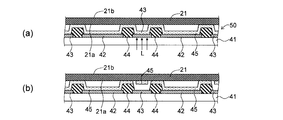
- the layer configuration of the organic semiconductor element 40 in the present embodiment will be described with reference to FIG.
- a top emission type organic EL element will be described as an example of the organic semiconductor element 40.
- the organic semiconductor element 40 includes a base material 41, a plurality of first electrodes 42 provided on the base material 41, auxiliary electrodes 43 and protrusions provided between the first electrodes 42. A portion 44, an organic semiconductor layer 45 provided on the first electrode 42, and a second electrode 46 provided on the organic semiconductor layer 45 and the auxiliary electrode 43.
- the organic semiconductor layer 45 includes at least a light emitting layer that emits light by recombination of electrons and holes in the organic compound.
- the organic semiconductor layer 45 may further include various layers generally provided in the organic EL element, such as a hole injection layer, a hole transport layer, an electron transport layer, or an electron injection layer.
- a hole injection layer such as a hole injection layer, a hole transport layer, an electron transport layer, or an electron injection layer.
- the first electrode 42 is provided corresponding to each of the organic semiconductor layers 45.
- the first electrode 42 also functions as a reflective electrode that reflects light generated in the organic semiconductor layer 45.
- Examples of the material constituting the first electrode 42 include simple elements of metal elements such as aluminum, chromium, titanium, iron, cobalt, nickel, molybdenum, copper, tantalum, tungsten, platinum, gold, and silver, or alloys thereof. it can.
- the second electrode 46 functions as a common electrode for the plurality of organic semiconductor layers 45.
- the second electrode 46 is configured to transmit light generated in the organic semiconductor layer 45.
- a material constituting the second electrode 46 a metal film thinned to such an extent that light can be transmitted, or an oxide conductive material such as ITO can be used.
- the auxiliary electrode 43 prevents a variation in voltage drop due to a difference in distance from a power source (not shown) to each organic semiconductor layer, thereby suppressing a variation in luminance of a display device using an organic EL element. Is to do. As shown in FIG. 1, each auxiliary electrode 43 is connected to the second electrode 46. Examples of the material constituting the auxiliary electrode 43 include a single element or alloy of the same metal element as that of the first electrode 42. The auxiliary electrode 43 may be made of the same material as the first electrode 42, or may be made of a material different from the first electrode 42.
- the protrusion 44 is made of an insulating material.
- the protrusion 44 is provided between the first electrode 42 and the auxiliary electrode 43.
- the shape of the organic semiconductor layer 45 provided between the protrusions 44 can be appropriately determined.
- a material constituting the protruding portion 44 an organic material such as polyimide or an inorganic insulating material such as silicon oxide can be used.
- the protruding portion 44 is configured to extend along the normal direction of the base material 41. Therefore, when the lid material described later is brought into close contact with the base material 41, a space is provided between the lid material and the base material 41. It can also function as a spacer for ensuring the above.
- the organic semiconductor layer 45 and the second electrode 46 may be continuously provided not only on the first electrode 42 but also on the protrusion 44.
- the organic semiconductor layer 45 emits light when current flows between the first electrode 42 and the second electrode 46.
- the organic semiconductor layer 45 located on the protrusion 44 the organic semiconductor layer 45 is positioned between the first electrode 42 and the second electrode 46. No light emission occurs. 2A and 2B to be described later, the portion of the organic semiconductor layer 45 that emits light, that is, the organic semiconductor layer 45 provided on the first electrode 42 is shown.
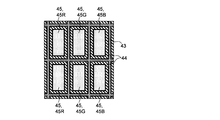
- FIG. 2A is a plan view illustrating an example of the layout of the auxiliary electrode 43, the protrusion 44, and the organic semiconductor layer 45.
- the organic semiconductor layer 45 may include a red organic semiconductor layer 45R, a green organic semiconductor layer 45G, and a blue organic semiconductor layer 45B that are arranged in order in a matrix and each have a rectangular shape.
- each of the red organic semiconductor layer 45R, the green organic semiconductor layer 45G, and the blue organic semiconductor layer 45B constitutes a sub-pixel.
- a combination of adjacent organic semiconductor layers 45R, 45G, and 45B constitutes one pixel.
- the auxiliary electrodes 43 are arranged in a grid so as to extend between the organic semiconductor layers 45 arranged in a matrix.
- the protrusion 44 is provided between the organic semiconductor layer 45 and the auxiliary electrode 43 so as to surround the organic semiconductor layer 45 provided on the first electrode 42 from the side. That is, the protrusions 44 are continuously provided along the four sides of the organic semiconductor layer 45 provided on the first electrode 42. Accordingly, it is possible to prevent the scattered organic semiconductor material from reaching the organic semiconductor layer 45 on the first electrode 42 in the step of removing the organic semiconductor layer 45 on the auxiliary electrode 43.
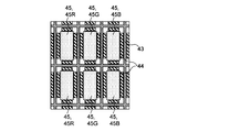
- the auxiliary electrode 43 does not need to be connected to the second electrode 46 over the entire area. That is, it is not necessary to remove all of the organic semiconductor layer 45 on the auxiliary electrode 43 in the removing step described later. Therefore, as shown in FIG. 2B, the protrusions 44 may be provided discontinuously along any of the four sides of the organic semiconductor layer 45. Also in the example shown in FIG. 2B, in the step of removing the organic semiconductor layer 45 on the auxiliary electrode 43 at the position sandwiched by the protrusions 44, the scattered organic semiconductor material is sandwiched at least partially by the protrusions 44. It is possible to prevent reaching the organic semiconductor layer 45 on the first electrode 42 located in the region. Further, by connecting the auxiliary electrode 43 located between the protrusions 44 to the second electrode 46, the voltage drop can be appropriately suppressed.
- the auxiliary electrode 43 is not particularly limited as long as the voltage drop of the second electrode 46 can be appropriately suppressed.
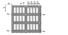
- the auxiliary electrode 43 may be provided along each pixel configured by organic semiconductor layers 45R, 45G, 45B, and 45W corresponding to a plurality of subpixels. That is, the auxiliary electrode 43 is not formed between the organic semiconductor layers 45R, 45G, 45B, and 45W, which are sub-pixels, and one pixel constituted by the organic semiconductor layers 45R, 45G, 45B, and 45W and the other similar ones.
- An auxiliary electrode 43 may be formed between these pixels.
- 2C and 2D show an example in which each pixel further includes a white organic semiconductor layer 45W in addition to the red organic semiconductor layer 45R, the green organic semiconductor layer 45G, and the blue organic semiconductor layer 45B as sub-pixels. ing.
- the arrangement of the location where the auxiliary electrode 43 and the second electrode 46 are connected is not particularly limited.
- the location where the auxiliary electrode 43 and the second electrode 46 are connected is indicated by a dotted line denoted by reference numeral 43x.
- the auxiliary electrode 43 and the second electrode 46 may be discretely connected at a plurality of locations. That is, the organic semiconductor layer 45 on the auxiliary electrode 43 may be discretely removed at a plurality of locations.
- the auxiliary electrode 43 and the second electrode 46 may be connected in a line along the direction in which the auxiliary electrode 43 extends.
- the organic semiconductor layer 45 on the auxiliary electrode 43 may be linearly removed along the direction in which the auxiliary electrode 43 extends.
- FIG. 2D shows an example in which the organic semiconductor layer 45 on the auxiliary electrode 43 is linearly removed along the direction D1 in which the lid member 21 described later is conveyed.
- 2A to 2D show examples in which a plurality of types of organic semiconductor layers 45R, 45G, 45B, and 45W are used as the organic semiconductor layer 45, the present invention is not limited to this.
- all of the organic semiconductor layers 45 constituting the sub-pixels may be configured to generate common white light.
- a color filter or the like can be used as means for color-coding each sub-pixel.
- the environment in which the element manufacturing method is implemented is not particularly limited.
- the element manufacturing method is partially under a vacuum environment.
- the specific pressure in the vacuum environment is not particularly limited as long as the pressure is lower than the atmospheric pressure.
- the internal pressure of the element manufacturing apparatus 10 is 1.0 ⁇ 10 4 Pa or less. It has become.
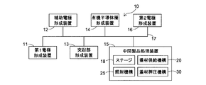
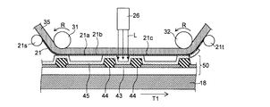
- FIG. 3 is a diagram schematically showing the element manufacturing apparatus 10.
- the element manufacturing apparatus 10 includes a first electrode forming apparatus 11 that forms a plurality of first electrodes 42 on a base material 41, and an auxiliary electrode formation that forms an auxiliary electrode 43 between the first electrodes 42.
- the device 12, the protrusion forming device 13 that forms the protrusion 44 between the first electrode 42 and the auxiliary electrode 43, and the organic semiconductor layer 45 is formed on the first electrode 42, the auxiliary electrode 43, and the protrusion 44.
- an organic semiconductor layer forming apparatus 14 In the following description, what is obtained by a process using each device 11, 12, 13, 14 may be referred to as an intermediate product 50.
- the element manufacturing apparatus 10 further includes an intermediate product processing apparatus 15 that performs a predetermined process while a lid material described later is in close contact with a part of the intermediate product 50.
- an example in which the intermediate product processing apparatus 15 is configured as a removing apparatus that removes the organic semiconductor layer 45 provided on the auxiliary electrode 43 will be described.
- the intermediate product processing apparatus 15 includes a stage 18, a lid material supply mechanism 20, a sealing mechanism 30, and an irradiation mechanism 25. Each component of the intermediate product processing apparatus 15 will be described later.
- the lid member 21 or the element manufacturing apparatus 10 further includes a second electrode type device 16 that forms the second electrode 46 on the auxiliary electrode 43 and the organic semiconductor layer 45 after the organic semiconductor layer 45 on the auxiliary electrode 43 is removed. ing.
- the element manufacturing apparatus 10 includes a transfer device 17 connected to each of the devices 11 to 16 in order to transfer the base material 41 and the intermediate product 50 between the devices 11 to 16 while maintaining a vacuum environment. May be further provided.
- FIG. 3 classifies each device from a functional viewpoint, and the physical form is not limited to the example shown in FIG.
- a plurality of devices among the devices 11 to 16 shown in FIG. 3 may be physically constituted by one device.
- any of the devices 11 to 16 shown in FIG. 3 may be physically configured by a plurality of devices.
- the first electrode 42 and the auxiliary electrode 43 may be formed simultaneously in one process.
- the first electrode forming device 11 and the auxiliary electrode forming device 12 may be configured as one device.
- a method for manufacturing the organic semiconductor element 40 using the element manufacturing apparatus 10 will be described.
- a metal material layer constituting the first electrode 42 and the auxiliary electrode 43 is formed on the substrate 41 by, for example, a sputtering method, and then the metal material layer is formed by etching.
- the first electrode 42 and the auxiliary electrode 43 described above can be simultaneously formed on the base material 41.
- the step of forming the first electrode 42 and the step of forming the auxiliary electrode 43 may be performed separately.
- the normal line of the base material 41 is interposed between the first electrode 42 and the auxiliary electrode 43 and above the first electrode 42 and the auxiliary electrode 43 by, for example, photolithography.
- a plurality of protrusions 44 extending in the direction are formed.
- a general film forming method such as a vapor deposition method, a CVD method, a printing method, an ink jet method, or a transfer method, the first electrode 42, the auxiliary electrode 43, and the protrusion 44
- An organic semiconductor layer 45 is formed thereon.
- An intermediate product 50 including the organic semiconductor layer 45 provided on the electrode 43 and the protrusion 44 can be obtained.
- the first electrode 42 and the auxiliary electrode 43 are formed on the base material 41 before the protrusion 44. For this reason, the first electrode 42 and the auxiliary electrode 43 are partially covered by the protrusion 44.
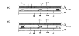
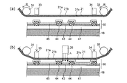
- the lid member 21 is prepared, and then the first surface 21a of the lid member 21 is brought into close contact with a part of the intermediate product 50 as shown in FIG.
- the organic semiconductor layer 45 provided on the auxiliary electrode 43 is irradiated with light L such as laser light, as shown in FIG. .
- the energy of the light L is absorbed by the organic semiconductor layer 45, and as a result, the organic semiconductor material constituting the organic semiconductor layer 45 on the auxiliary electrode 43 is scattered. In this way, the organic semiconductor layer 45 on the auxiliary electrode 43 can be removed.
- the organic semiconductor material scattered from the auxiliary electrode 43 adheres to the first surface 21a of the lid member 21, for example, as shown in FIG.
- FIG. 4F is a diagram showing a state where the organic semiconductor layer 45 on the auxiliary electrode 43 has been removed.
- the second electrode 46 is formed on the organic semiconductor layer 45 on the first electrode 42 and on the auxiliary electrode 43.
- the organic semiconductor element 40 including the auxiliary electrode 43 connected to the second electrode 46 can be obtained.
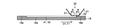
- FIG. 5 the method for bringing the lid material 21 into close contact with a part of the intermediate product 50 and removing the organic semiconductor layer 45 on the auxiliary electrode 43 described with reference to FIGS. This will be described in more detail with reference to FIG. Note that the steps shown in FIGS. 4D and 4E are performed by the intermediate product processing apparatus 15 described above. First, the configuration of the intermediate product processing apparatus 15 will be described in detail with reference to FIG. In FIG. 5, the first direction, the second direction, and the third direction orthogonal to each other are indicated by arrows D1, D2, and D3, respectively.
- the intermediate product processing apparatus 15 includes a stage 18 on which the intermediate product 50 is placed, a lid material supply mechanism 20 that supplies a long lid material 21, and a part of the lid material 21.
- a sealing mechanism 30 that is in close contact with a part of the intermediate product 50 and an irradiation mechanism 25 that irradiates light to a portion of the intermediate product 50 where the lid member 21 is in close contact are provided.
- Each component of the intermediate product processing apparatus 15 is disposed in a chamber maintained in a vacuum atmosphere. For this reason, the process of removing the organic semiconductor layer 45 on the auxiliary electrode 43 can be performed in a vacuum environment.
- “long” means that the size of the lid 21 in the direction in which the lid 21 is conveyed is at least five times the dimension of the lid 21 in the direction perpendicular to the direction in which the lid 21 is conveyed. It means that
- stage 18 The stage 18 has a mounting surface 18a for supporting the intermediate product 50, and the mounting surface 18a extends in parallel with the first direction D1 and the second direction D2.
- the stage 18 is configured to be movable in a stage moving direction T1 parallel to the first direction D1.
- the intermediate product 50 is placed on the stage 18 so that the plurality of protrusions 44 described above are arranged on the base material 41 along the first direction D1. For this reason, as will be described later, by repeating the movement of the stage 18 along the stage moving direction T1 and the irradiation mechanism 25 irradiating the light toward the intermediate product 50, the first of the intermediate products 50.
- the protrusion 44 of the intermediate product 50 placed on the stage 18 extends along a third direction D3 orthogonal to the first direction D1 and the second direction D2.
- the sealing mechanism 30 includes a pair of rollers 31 and 32 that rotate in a rotation direction R around a rotation axis that extends in a second direction D2 orthogonal to the first direction D1.
- the pair of rollers 31 and 32 includes a first roller 31 and a second roller 32.
- the lid supply mechanism 20 is not shown, but the feeding portion that feeds the lid 21 along the feeding direction T2 between the first roller 31 and the intermediate product 50, the second roller 32, and the intermediate product. And a winding portion that winds the lid member 21 after passing through 50 along the winding direction T3.
- the lid member 21 for covering a part of the intermediate product 50 is supplied in a roll-to-roll manner.
- a surface facing the stage 18 side of the surface of the lid member 21 is referred to as a first surface 21a
- a surface on the opposite side of the first surface 21a is referred to as a second surface 21b.
- Each of the rollers 31 and 32 is in contact with the second surface 21b of the lid member 21.
- PET polyethylene terephthalate
- COP cycloolefin polymer
- PP polypropylene
- PE polyethylene
- PC polycarbonate
- the rollers 31 and 32 of the sealing mechanism 30 are configured to rotate in synchronization with the movement of the stage 18. That is, each roller 31 and 32 conveys the cover material 21 wound around each roller 31 and 32 so that the moving speed of the stage 18 and the conveyance speed of the cover material 21 coincide.
- Each of the rollers 31 and 32 is configured not only to transport the lid member 21 but also to apply a predetermined tension to the lid member 21 positioned between the first roller 31 and the second roller 32. Yes. For this reason, it can be said that the part located between the 1st roller 31 and the 2nd roller 32 among the cover materials 21 exists in the state stretched by a pair of rollers 31 and 32.
- a portion of the lid member 21 that is stretched between the pair of rollers 31 and 32 is also referred to as a stretched portion 21c.
- each of the pair of rollers 31 and 32 is provided with a drive unit for supporting and rotating the rollers 31 and 32 at predetermined positions.
- the specific configuration of the drive unit for rotating the rollers 31 and 32 is not particularly limited.
- the irradiation mechanism 25 has an optical head 26 that emits light L such as laser light. The light emitted from the optical head 26 passes through the stretched portion 21 c of the lid member 21 and reaches the intermediate product 50.
- the irradiation mechanism 25 may further include a lens for focusing the light L with respect to the organic semiconductor layer 45.
- the optical head 26 is fixed with respect to the movement of the stage 18 and the rotation of the roller 31. That is, they are arranged independently from the stage 18 and the roller 31.
- the optical head 26 is configured so that the traveling direction of the light L generated by the optical head 26 does not change even if the stage 18 moves or the roller 31 rotates.
- the stage 18 is movable in the first direction D1, and the protrusions 44 of the intermediate product 50 are arranged along the first direction D1. Therefore, even when the optical head 26 is in a stationary state, it is possible to sequentially irradiate the plurality of protrusions 44 or their peripheral portions with light.
- the aim of the optical head 26 is not shifted during the process. Accordingly, it is possible to irradiate light with higher positional accuracy than when irradiating light to a plurality of portions of the intermediate product 50 while moving the optical head 26.
- the optical head 26 may be configured to be movable in the second direction D2, that is, in the direction along the rotation axis of each of the rollers 31 and 32, as indicated by an arrow M in FIG. This makes it possible to irradiate an arbitrary part of the intermediate product 50 with light, as will be described later.
- a specific configuration for moving the optical head 26 is not particularly limited.
- the optical head 26 can move along a rail 27 disposed above the stage 18.
- the second direction is used when the optical head 26 is configured to be able to selectively extract light at an arbitrary position in the second direction. It becomes possible to irradiate the light toward the intermediate product 50 at any position.
- a mask in which a plurality of openings are formed is disposed between the irradiation mechanism 25 and the lid member 21, and A method of selectively shielding the opening of the mask is conceivable.
- the portion of the intermediate product 50 that is to be irradiated with light is along the first direction orthogonal to the second direction. It does not have to be lined up. Accordingly, although not shown, the protrusions 44 of the intermediate product 50 do not have to be arranged along the first direction D1.
- the lid member 21 having the first surface 21 a is prepared so that the first surface 21 a faces the protruding portion 44 side of the intermediate product 50.
- a lid material supply step of supplying the lid material 21 between the first roller 31 and the intermediate product 50 so that the first surface 21 a of the lid material 21 faces the stage 18 side is performed.
- a sealing step of pressing a part of the first surface 21 a of the lid member 21 against the intermediate product 50 using the pair of rollers 31 and 32 of the sealing mechanism 30 is performed. Thereby, a part of the first surface 21 a of the lid member 21 is in close contact with a part of the intermediate product 50. Specifically, as shown in FIG.
- the first surface 21 a of the stretched portion 21 c of the lid member 21 is in close contact with a part of the intermediate product 50.
- a predetermined tension is applied to the stretched portion 21 c of the lid member 21 stretched between the pair of rollers 31 and 32.
- abuts to a pair of rollers 31 and 32 among the cover materials 21 is each pressed toward the intermediate product 50, as shown in FIG.
- the tension part 21c between a pair of rollers 31 and 32 is pressed with respect to the intermediate product 50 with predetermined pressure. It is in the state where it was done. For example, in the example illustrated in FIG.
- the stretched portion 21 c is pressed against the portion of the intermediate product 50 where the protrusion 44 is provided with a predetermined pressure. Therefore, the first surface 21a of the lid member 21 can be closely attached to the portion of the intermediate product 50 where the protrusion 44 is provided without any gap.
- an irradiation step of irradiating the intermediate product 50 with light through the lid member 21 is performed on a portion of the intermediate product 50 that is in close contact with the lid member 21.
- the “part in close contact with the lid member 21” means not only the portion of the protrusion 44 that is in direct contact with the first surface 21 a of the lid member 21 but also the first surface 21 a of the lid member 21. This is a concept including a portion surrounded by the protruding portion 44. Note that it is not necessary to irradiate all the portions of the intermediate product 50 that are in close contact with the lid member 21.
- the light is irradiated to a portion of the intermediate product 50 that is in close contact with the lid member 21 and that is provided with the organic semiconductor layer 45 to be removed.
- the organic semiconductor layer 45 absorbs the energy of the light L, the organic semiconductor material constituting the organic semiconductor layer 45 on the auxiliary electrode 43 is scattered as described above.
- the stretched portion 21c that is tensioned with a predetermined tension is formed on the lid member 21, and this stretched portion 21c is intermediate product with a predetermined pressure. It is pressed against a part of 50. For this reason, the 1st surface 21a of the stretch part 21c of the cover material 21 can be closely_contact
- the organic semiconductor element 40 having high quality can be manufactured at a low cost.
- the organic semiconductor layer 45 on the auxiliary electrode 43 is removed, the light from the irradiation mechanism 25 is stopped. That is, the light irradiation to the intermediate product 50 is stopped.
- the stage 18 is moved along the stage moving direction T1, and the lid member 21 is moved along the rotation direction R of the rollers 31 and 32.
- the irradiation mechanism 25 emits light again.
- the light L from the irradiation mechanism 25 is again irradiated to the organic semiconductor layer 45 on the auxiliary electrode 43, and thereby the organic semiconductor layer 45 is removed.
- the organic semiconductor layers 45 on the plurality of auxiliary electrodes 43 arranged along the first direction D1 parallel to the stage moving direction T1 can be sequentially removed.
- the organic semiconductor layers 45 on the auxiliary electrode 43 are arranged at equal intervals on the base material 41. Accordingly, light emission from the irradiation mechanism 25 is turned on and off at a constant cycle considering the interval between the auxiliary electrodes 43 and the moving speed of the stage 18, and thereby the organic semiconductor layer 45 on the auxiliary electrode 43 is sequentially irradiated with light. May be.
- the optical head 26 of the irradiation mechanism 25 remains stationary as described above. For this reason, according to the present embodiment, it is possible to irradiate light to the intermediate product 50 with high positional accuracy, and thereby, the organic semiconductor layer 45 of the auxiliary electrode 43 can be accurately removed.
- the intermediate product 50 on the moving stage 18 it is possible to cover the intermediate product 50 on the moving stage 18 by using the lid 21 supplied in a roll-to-roll manner. For this reason, the above-mentioned process of removing the organic semiconductor layer 45 on the auxiliary electrode 43 can be performed on the plurality of intermediate products 50 using one roll body around which the lid member 21 is wound. Therefore, an apparatus or process for cutting the lid member 21 for each intermediate product 50 is not necessary, and therefore the apparatus configuration and process can be simplified. Moreover, the waste resulting from the cutting
- the rail 27 The optical head 26 may be moved along After the optical head 26 is moved, the organic semiconductor layer 45 on the plurality of auxiliary electrodes 43 positioned on a new line can be removed by performing the above-described process again while moving the stage 18.
- a plurality of protrusions 44 are formed on the base material 41.
- the first electrode 42 is formed between the protrusions 44, and the auxiliary electrode 43 is formed on the protrusions 44.
- a plurality of first electrodes 42 insulated from each other by the protrusions 44 and the auxiliary electrodes 43 provided on the protrusions 44 can be obtained.
- the first electrode 42 is formed on the base material 41, then the projection 44 is formed between the first electrodes 42, and then the auxiliary electrode 43 is formed on the projection 44. May be. Thereafter, as shown in FIG.
- an organic semiconductor layer 45 is formed on the first electrode 42, the auxiliary electrode 43, and the protrusion 44.
- the base material 41, the plurality of first electrodes 42 provided on the base material 41, the auxiliary electrode 43 and the protrusion 44 provided between the first electrodes 42, the first electrode 42 and the auxiliary An intermediate product 50 including the organic semiconductor layer 45 provided on the electrode 43 can be obtained.
- the protrusion 44 is formed before the auxiliary electrode 43, so that the protrusion 44 is covered with the auxiliary electrode 43.
- the protrusion 44 does not need to be covered with the auxiliary electrode 43 over the entire upper surface. That is, the upper surface of the protrusion 44 only needs to be at least partially covered by the auxiliary electrode 43.
- the example in which the protrusions 44 are provided in two rows between the first electrodes 42 and the auxiliary electrode 43 is provided between the protrusions 44 has been described. Since the electrodes 43 are provided on the protrusions 44, the protrusions 44 provided between the first electrodes 42 may be in only one row as shown in FIG.
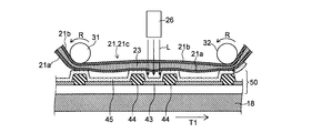
- the stretched portion 21 c of the lid member 21 is pressed against a part of the intermediate product 50 using a pair of rollers 31 and 32 of the sealing mechanism 30, whereby the lid member A lid material adhesion process is performed in which a part of the first surface 21 a of 21 is adhered to a part of the intermediate product 50.
- the stage 18 on which the intermediate product 50 is placed is omitted.
- portions of the lid member 21 that are in contact with the pair of rollers 31 and 32 are each pressed toward the intermediate product 50. For this reason, not only the part which contact
- FIG. 7F is a diagram showing a state where the organic semiconductor layer 45 on the auxiliary electrode 43 on the protrusion 44 is removed.
- the lid member 21 is in close contact with the organic semiconductor layer 45 to be removed.
- the organic semiconductor layer 45 on the auxiliary electrode 43 on the protruding portion 44 can be attached to the first layer 21 of the lid member 21 without irradiating the light L. It is also possible to transfer to the first surface 21a. That is, it is possible to remove the organic semiconductor layer 45 provided on the auxiliary electrode 43 by closely attaching the stretched portion 21 c of the lid member 21 to a part of the intermediate product 50.
- the second electrode 46 is formed on the organic semiconductor layer 45 on the first electrode 42 and on the auxiliary electrode 43 on the protrusion 44.
- the organic semiconductor element 40 including the auxiliary electrode 43 connected to the second electrode 46 can be obtained.
- the intermediate product processing apparatus 15 is configured as an exposure apparatus
- the example in which the intermediate product processing apparatus 15 is used as a removing apparatus that removes the organic semiconductor layer 45 on the auxiliary electrode 43 is shown.
- the application example of the intermediate product processing apparatus 15 is not particularly limited.
- the intermediate product processing apparatus 15 performs an exposure process of irradiating the exposure layer in the intermediate product 50 with light L as exposure light while the lid 21 is in close contact with the intermediate product 50. It may be used as an exposure apparatus.
- the intermediate product processing apparatus 15 irradiates the vapor deposition material 48 with light while the lid 21 is in close contact with the intermediate product 50, and the vapor deposition material 48. May be used as a vapor deposition apparatus for vapor-depositing the material on the substrate 41.
- the vapor deposition material 48 is provided on the first surface 21a of the lid member 21 as shown in FIG. 8A
- the intermediate product 50 includes a base material 41, a plurality of protrusions 44 provided on the base material 41, a first electrode 42 provided between the protrusions 44, have.
- the vapor deposition material 48 evaporates. More specifically, as shown in FIG. 8A, when the vapor deposition material 48 existing at a position facing the first electrode 42 in the vapor deposition material 48 is irradiated with light L, the vapor deposition material 48 evaporates.
- a vapor deposition layer 49 can be formed on the first electrode 42 as shown in FIG. Further, the space between the base material 41 and the lid member 21 is appropriately partitioned by the protrusions 44. For this reason, it is possible to prevent the vapor deposition material 48 from being scattered over a wide area in the space between the base material 41 and the lid member 21.
- the method of heating and evaporating the vapor deposition material 48 is not limited to the above.
- a metal thin film that absorbs infrared light is formed between the first surface 21a of the lid member 21 and the organic semiconductor layer 45, and the metal thin film is irradiated with light to heat the metal thin film, thereby vapor deposition.
- the material 48 may be heated.
- the vapor deposition material 48 provided on the first surface 21a of the lid member 21 is hardly directly irradiated with light, but the vapor deposition material 48 can be indirectly heated through the metal thin film. Therefore, the vapor deposition material 48 can be evaporated.
- a magnetic field is generated around the lid member 21 or the lid member 21 of the intermediate product 50 is generated in order to further increase the degree of adhesion of the lid member 21 to the intermediate product 50.
- a magnetic material may be disposed on the opposite side of the lid member 21 so that the lid member 21 is drawn toward the intermediate product 50 by a magnetic force.
- the stage 18 on which the intermediate product 50 is placed protrudes in the normal direction of the base material 41 so as to be adjacent to the end of the base material 41 of the intermediate product 50 in the first direction D1.
- Region 18b may be formed.
- the protruding region 18 b is configured such that the position of the upper surface thereof substantially coincides with the position of the upper surface of the intermediate product 50.
- the pair of rollers 31 and 32 is configured such that one roller, for example, the first roller 31 is positioned on the intermediate product 50 via the lid member 21, and the other roller, for example, the second roller 32 is disposed via the lid member 21.
- the lid member 21 can be stretched while being positioned on the protruding region 18 b of the stage 18.
- the stretched portion 21 c of the lid member 21 can be positioned in the vicinity of the end portion of the base material 41 of the intermediate product 50. This makes it possible to closely attach the stretched portion 21 c of the lid member 21 to a portion of the intermediate product 50 in the vicinity of the end portion of the base material 41. Therefore, the process using the intermediate product processing apparatus 15 can be performed on the entire area of the intermediate product 50.
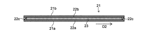
- the lid member 21 is configured by a single layer made of a light-transmitting material.
- the lid member 21 may be composed of a plurality of layers.
- the lid member 21 may include a first film 22a and a second film 22b.
- the first film 22a constitutes the first surface 21a of the lid member 21 facing the stage 18 side
- the second film 22b constitutes the second surface 21b on the opposite side of the first surface 21a.
- FIG. 10 is a cross-sectional view showing the case where the lid member 21 is cut along the second direction D2 described above, that is, along the direction of the rotation axis of the rollers 31 and 32.
- a sealing material 22c may be interposed between the first film 22a and the second film 22b.
- the sealing material 22c extended along the length direction of each film 22a, 22b is provided in the edge part vicinity of each film 22a, 22b in the 2nd direction D2, respectively.
- a space is provided between the first film 22a and the second film 22b, and the space 23 between the first film 22a and the second film 22b is sealed from the outside. It becomes possible to do. For example, it becomes possible to enclose a gas such as air or nitrogen in the space between the first film 22a and the second film 22b. Advantages of using the lid member 21 in which the gas is sealed in the internal space 23 will be described below with reference to FIG.
- the sealing step in which the first surface 21a of the lid 21 is in close contact with a part of the intermediate product 50 is performed in a reduced pressure environment having a pressure lower than the atmospheric pressure, such as a vacuum environment.
- the gas is sealed between the first film 22a and the second film 22b
- the gas is sealed in the lid member 21 based on the difference between the pressure of the gas and the pressure under the reduced pressure environment.
- the gas expands.
- the interval between the first film 22a and the second film 22b tends to increase. That is, the films 22a and 22b try to swell outward.
- the distance between the first film 22 a and the second film 22 b is the distance between the intermediate product 50 and the rollers 31 and 32.
- the first film 22 a is intermediate based on the gas expansion.
- the product 50 swells toward a space where the protruding portion 44 does not exist. This means that the first film 22a is more closely attached to the portion of the intermediate product 50 where the protrusions 44 are provided, compared to the case where such swelling does not occur.
- the first surface 21a of the lid member 21 constituted by the first film 22a can be brought into close contact with the portion of the intermediate product 50 where the protrusions 44 are provided without any gaps. It becomes like this. This can more reliably prevent the organic semiconductor material scattered from the auxiliary electrode 43 from contaminating the organic semiconductor layer 45 on the first electrode 42 and the surrounding environment.
- the specific structure of the cover material 21 is not specifically limited.
- a hollow resin having a large number of hollow portions may be provided between the first film 22a and the second film 22b.
- a gas such as air is present in the hollow portion of the hollow resin. Therefore, when the lid 21 provided with the hollow resin is placed in a vacuum environment, the gas in the hollow portion of the hollow resin expands, As a result, the films 22a and 22b swell outward. Further, by providing the hollow resin, the interval between the first film 22a and the second film 22b can be stably maintained.
- the hollow resin for example, a resin containing hollow particles made of styrene, acrylic, silica, or the like, or a resin having a hollow structure such as porous silica can be used.
- the sealing mechanism 30 may have an intermediate film provided between the pair of rollers 31 and 32 and the lid member 21.
- the long intermediate film unwound from the unillustrated unwinding section is conveyed along the pair of rollers 31 and 32 and then wound by the unillustrated winding section. Yes.
- the pair of rollers 31 and 32 press the lid 21 toward the intermediate product 50 through the intermediate film 35. Therefore, also in this modification, as in the case of the above-described embodiment, the stretched portion 21c between the pair of rollers 31 and 32 of the lid member 21 is connected to the intermediate product 50 via the intermediate film 35. And pressed at a predetermined pressure. Therefore, the first surface 21a of the lid member 21 can be closely attached to the portion of the intermediate product 50 where the protrusion 44 is provided without any gap.
- the pressing force and tension received by the lid member 21 are not directly applied to the lid member 21 from the pair of rollers 31 and 32 but are applied to the lid member 21 via the intermediate film 35.
- the intermediate film 35 is in contact with the lid member 21 over a wide area at a portion located between the pair of rollers 31 and 32.
- deformation transformation, such as a wrinkle, arises in the cover material 21 resulting from the pressing force and tension
- the lid member 21 unwound from the unwinding portion 21s covers the intermediate product 50 in a state of being overlapped with the intermediate film 35, and then is separated from the intermediate film 35 and wound by the winding portion 21t.
- the material constituting the intermediate film 35, the thickness and the layer structure of the intermediate film 35, and the like are selected so that a suitable pressing force or tension can be applied to the lid member 21 via the intermediate film 35.
- a material having a higher elastic coefficient than the material constituting the lid member 21 is used as the material constituting the intermediate film 35.
- the intermediate film 35 is curved so as to protrude toward the intermediate product 50 between the pair of rollers 31 and 32.
- the lid member 21 may be pressed more strongly against the product 50.
- the intermediate film 35 may include a pair of films and an interference layer provided between the pair of films.
- the pair of films for example, a pair of PET films each having a thickness in the range of 100 ⁇ m to 500 ⁇ m can be used.
- the gel-form material which has translucency can be used as a material which comprises an interference layer.
- an optical adhesive material having translucency so-called OCA can be used.
- the organic semiconductor material scattered from the auxiliary electrode 43 of the intermediate product 50 adheres to the first surface 21a of the lid member 21. Therefore, in order to manufacture the organic semiconductor element 40 having high quality, it is preferable that the lid member 21 to which the organic semiconductor material is attached is discarded without being reused in the manufacturing process of the organic semiconductor element 40. On the other hand, the organic semiconductor material does not adhere to the intermediate film 35. Moreover, as shown in FIG. 12, the cover material 21 and the intermediate film are separated and collected separately. Therefore, it is possible to reuse the intermediate film 35 in the manufacturing process of the organic semiconductor element 40 performed thereafter.
- a pair of rollers 31 and 32 are used as a pair of stretching members for applying tension to the lid member 21.
- the specific configuration of the pair of stretching members is not particularly limited as long as tension can be applied to the portion of the lid member 21 that covers the intermediate product 50.
- the pair of stretching members 33 and 34 of the sealing mechanism 30 can move toward the intermediate product 50 so as to press the lid 21 toward the intermediate product 50.
- It may be a pair of members configured as described above.
- the lid member 21 is conveyed by the pair of rollers 31 and 32 when the stretching members 33 and 34 are not in contact with the second surface 21 b of the lid member 21. Is done.
- FIG. 13 (b) in a state where the pair of rollers 31, 32 are stopped, the pair of stretching members 33, 34 are moved toward the intermediate product 50, and the pair of stretching members 33, 34 is brought into contact with the second surface 21 b of the lid member 21.
- the auxiliary electrode 43 is generally composed of a single metal element or an alloy.
- the light L emitted toward the lid member 21 that is in close contact with the intermediate product 50 is mainly shielded by the auxiliary electrode 43.
- light having a wavelength that can be absorbed by the auxiliary electrode 43 is used as the light L, whereby the auxiliary electrode 43 can be heated and thereby the organic semiconductor layer 45 on the auxiliary electrode 43 can be heated.
- the organic semiconductor layer 45 on the auxiliary electrode 43 can be evaporated and adhered onto the first surface 21 a of the lid member 21.
- a material that can absorb the light L may be used as the material constituting the auxiliary electrode 43.
- the stage 18 is used as a support mechanism for supporting the intermediate product 50
- the specific configuration of the support mechanism that supports the intermediate product 50 is not particularly limited as long as the intermediate product 50 can be appropriately supported when the lid 21 is brought into close contact with the intermediate product 50.
- the unwinding unit that unwinds the intermediate product 50, the winding unit that winds up the intermediate product 50, and the intermediate product 50 that is being transported are in contact with each other.
- a transport roll, a guide roll, or the like may function as a support mechanism that supports the intermediate product 50.
- the base material 41 of the intermediate product 50 extends in a long shape, and the first electrode 42 and the auxiliary electrode 43 of the intermediate product 50 are also provided.
- the projecting portion 44, the organic semiconductor layer 45, the second electrode 46, and the like are formed on a base material 41 extending in a long shape.
- the organic semiconductor element 40 is an organic EL
- the type of the organic semiconductor element manufactured by the above-described element manufacturing apparatus 10 and the element manufacturing method is not particularly limited.
- organic transistor device known organic semiconductor layers and other components can be used, for example, those described in JP-A-2009-87996.
- organic solar cell device known photoelectric conversion layers composed of organic semiconductor layers and other components can be used, for example, those described in JP2011-151195A Can do.
- the element manufacturing apparatus 10 and the element manufacturing method described above may be applied not only to the manufacture of organic semiconductor elements but also to the manufacture of inorganic semiconductor elements.
- each component of the intermediate product processing apparatus 15 is disposed in a chamber maintained in a vacuum atmosphere. That is, the example in which the step of irradiating the intermediate product 50 with light using the intermediate product processing apparatus 15 is performed in a vacuum environment is shown.
- the present invention is not limited to this, and the step of irradiating the intermediate product 50 with light using the intermediate product processing apparatus 15 may be performed under an environment other than the vacuum environment such as an atmospheric pressure environment.
Landscapes
- Engineering & Computer Science (AREA)
- Physics & Mathematics (AREA)
- Optics & Photonics (AREA)
- Plasma & Fusion (AREA)
- Mechanical Engineering (AREA)
- Manufacturing & Machinery (AREA)
- Electroluminescent Light Sources (AREA)
- High Energy & Nuclear Physics (AREA)
- Electromagnetism (AREA)
- Health & Medical Sciences (AREA)
- Toxicology (AREA)
- Condensed Matter Physics & Semiconductors (AREA)
- General Physics & Mathematics (AREA)
- Computer Hardware Design (AREA)
- Microelectronics & Electronic Packaging (AREA)
- Power Engineering (AREA)
Priority Applications (3)
| Application Number | Priority Date | Filing Date | Title |
|---|---|---|---|
| US14/913,417 US9592572B2 (en) | 2013-08-20 | 2014-07-31 | Element manufacturing method and element manufacturing apparatus |
| KR1020167002346A KR20160044463A (ko) | 2013-08-20 | 2014-07-31 | 소자 제조 방법 및 소자 제조 장치 |
| CN201480041696.0A CN105409329B (zh) | 2013-08-20 | 2014-07-31 | 元件制造方法以及元件制造装置 |
Applications Claiming Priority (2)
| Application Number | Priority Date | Filing Date | Title |
|---|---|---|---|
| JP2013170723 | 2013-08-20 | ||
| JP2013-170723 | 2013-08-20 |
Publications (1)
| Publication Number | Publication Date |
|---|---|
| WO2015025692A1 true WO2015025692A1 (ja) | 2015-02-26 |
Family
ID=52483473
Family Applications (1)
| Application Number | Title | Priority Date | Filing Date |
|---|---|---|---|
| PCT/JP2014/070238 Ceased WO2015025692A1 (ja) | 2013-08-20 | 2014-07-31 | 素子製造方法および素子製造装置 |
Country Status (5)
| Country | Link |
|---|---|
| US (1) | US9592572B2 (enExample) |
| JP (2) | JP5800258B2 (enExample) |
| KR (1) | KR20160044463A (enExample) |
| CN (1) | CN105409329B (enExample) |
| WO (1) | WO2015025692A1 (enExample) |
Cited By (1)
| Publication number | Priority date | Publication date | Assignee | Title |
|---|---|---|---|---|
| US20150263284A1 (en) * | 2012-06-21 | 2015-09-17 | Osram Oled Gmbh | Method for closely connecting an organic optoelectronic component to a connection piece, connection structure for force-locking connecting, and optoelectronic component device |
Families Citing this family (4)
| Publication number | Priority date | Publication date | Assignee | Title |
|---|---|---|---|---|
| TWI634685B (zh) * | 2017-05-25 | 2018-09-01 | 機光科技股份有限公司 | 有機發光裝置 |
| FR3073324B1 (fr) * | 2017-11-08 | 2019-10-25 | Commissariat A L'energie Atomique Et Aux Energies Alternatives | Procede utilisant un laser pour le soudage entre deux materiaux metalliques ou pour le frittage de poudre(s), application a la realisation de plaques bipolaires pour piles pemfc |
| JP7520486B2 (ja) * | 2019-04-25 | 2024-07-23 | 大日本印刷株式会社 | 有機エレクトロルミネッセンス表示装置及びその製造方法 |
| CN110571361B (zh) * | 2019-09-17 | 2022-09-30 | 合肥鑫晟光电科技有限公司 | 有机发光显示面板及制作方法、显示装置 |
Citations (5)
| Publication number | Priority date | Publication date | Assignee | Title |
|---|---|---|---|---|
| JP2004079325A (ja) * | 2002-08-16 | 2004-03-11 | Fuji Photo Film Co Ltd | 有機電界発光素子の製造方法及び転写材料 |
| JP2006175840A (ja) * | 2004-12-20 | 2006-07-06 | Samsung Sdi Co Ltd | レーザ熱転写装置,レーザ熱転写方法,及び有機電界発光素子の製造方法 |
| JP2008288074A (ja) * | 2007-05-18 | 2008-11-27 | Sony Corp | 表示装置の製造方法 |
| WO2014157658A1 (ja) * | 2013-03-29 | 2014-10-02 | 大日本印刷株式会社 | 素子製造方法および素子製造装置 |
| WO2014157657A1 (ja) * | 2013-03-29 | 2014-10-02 | 大日本印刷株式会社 | 素子製造方法および素子製造装置 |
Family Cites Families (6)
| Publication number | Priority date | Publication date | Assignee | Title |
|---|---|---|---|---|
| JP4151421B2 (ja) * | 2003-01-23 | 2008-09-17 | セイコーエプソン株式会社 | デバイスの製造方法 |
| CN101803008B (zh) * | 2007-09-07 | 2012-11-28 | 株式会社半导体能源研究所 | 半导体装置及其制造方法 |
| JP2009087996A (ja) | 2007-09-27 | 2009-04-23 | Dainippon Printing Co Ltd | 有機半導体素子、有機半導体素子の製造方法、有機トランジスタアレイ、およびディスプレイ |
| JP2011009498A (ja) | 2009-06-26 | 2011-01-13 | Dainippon Printing Co Ltd | 有機エレクトロルミネッセンス素子 |
| JP2011113936A (ja) * | 2009-11-30 | 2011-06-09 | Fujifilm Corp | 光熱変換シート及び有機電界発光装置の製造方法 |
| JP2011151195A (ja) | 2010-01-21 | 2011-08-04 | Dainippon Printing Co Ltd | 有機薄膜太陽電池およびその製造方法 |
-
2014
- 2014-07-31 WO PCT/JP2014/070238 patent/WO2015025692A1/ja not_active Ceased
- 2014-07-31 KR KR1020167002346A patent/KR20160044463A/ko not_active Withdrawn
- 2014-07-31 CN CN201480041696.0A patent/CN105409329B/zh not_active Expired - Fee Related
- 2014-07-31 US US14/913,417 patent/US9592572B2/en not_active Expired - Fee Related
- 2014-07-31 JP JP2014156551A patent/JP5800258B2/ja not_active Expired - Fee Related
-
2015
- 2015-08-31 JP JP2015170580A patent/JP2016027571A/ja active Pending
Patent Citations (5)
| Publication number | Priority date | Publication date | Assignee | Title |
|---|---|---|---|---|
| JP2004079325A (ja) * | 2002-08-16 | 2004-03-11 | Fuji Photo Film Co Ltd | 有機電界発光素子の製造方法及び転写材料 |
| JP2006175840A (ja) * | 2004-12-20 | 2006-07-06 | Samsung Sdi Co Ltd | レーザ熱転写装置,レーザ熱転写方法,及び有機電界発光素子の製造方法 |
| JP2008288074A (ja) * | 2007-05-18 | 2008-11-27 | Sony Corp | 表示装置の製造方法 |
| WO2014157658A1 (ja) * | 2013-03-29 | 2014-10-02 | 大日本印刷株式会社 | 素子製造方法および素子製造装置 |
| WO2014157657A1 (ja) * | 2013-03-29 | 2014-10-02 | 大日本印刷株式会社 | 素子製造方法および素子製造装置 |
Cited By (2)
| Publication number | Priority date | Publication date | Assignee | Title |
|---|---|---|---|---|
| US20150263284A1 (en) * | 2012-06-21 | 2015-09-17 | Osram Oled Gmbh | Method for closely connecting an organic optoelectronic component to a connection piece, connection structure for force-locking connecting, and optoelectronic component device |
| US9941473B2 (en) * | 2012-06-21 | 2018-04-10 | Osram Oled Gmbh | Method for closely connecting an organic optoelectronic component to a connection piece, connection structure for force-locking connecting, and optoelectronic component device |
Also Published As
| Publication number | Publication date |
|---|---|
| JP2016027571A (ja) | 2016-02-18 |
| CN105409329A (zh) | 2016-03-16 |
| US20160207146A1 (en) | 2016-07-21 |
| JP2015062171A (ja) | 2015-04-02 |
| CN105409329B (zh) | 2017-10-24 |
| JP5800258B2 (ja) | 2015-10-28 |
| KR20160044463A (ko) | 2016-04-25 |
| US9592572B2 (en) | 2017-03-14 |
Similar Documents
| Publication | Publication Date | Title |
|---|---|---|
| JP2015046392A (ja) | 素子製造方法および素子製造装置 | |
| JP5800258B2 (ja) | 素子製造方法および素子製造装置 | |
| JP6510129B2 (ja) | 蒸着マスク、蒸着マスクの製造方法および有機半導体素子の製造方法 | |
| KR20110087830A (ko) | 레이저 열전사 장치 및 이를 이용한 유기 발광 표시 장치의 제조방법 | |
| JP6164529B2 (ja) | 素子製造方法および素子製造装置 | |
| US20070178402A1 (en) | Laser irradiation device and method of fabricating organic light emitting display device using the same | |
| JP5880611B2 (ja) | 素子製造方法および素子製造装置 | |
| JP2013065446A (ja) | 薄膜パターン形成方法 | |
| JP2012038574A (ja) | 表示装置の製造方法 | |
| US9882173B2 (en) | Methods for fabricating an organic electro-luminescence device | |
| JP2013077541A5 (ja) | 薄膜パターン形成方法、それに使用するマスク、マスクの製造方法及び有機el表示装置の製造方法 | |
| JP6221667B2 (ja) | 素子製造方法および素子製造装置 | |
| JP2015069899A (ja) | 素子製造方法および素子製造装置 | |
| JP2016062839A (ja) | 素子製造方法 | |
| JP2016062036A (ja) | 表示素子製造方法および表示素子 |
Legal Events
| Date | Code | Title | Description |
|---|---|---|---|
| WWE | Wipo information: entry into national phase |
Ref document number: 201480041696.0 Country of ref document: CN |
|
| 121 | Ep: the epo has been informed by wipo that ep was designated in this application |
Ref document number: 14837483 Country of ref document: EP Kind code of ref document: A1 |
|
| ENP | Entry into the national phase |
Ref document number: 20167002346 Country of ref document: KR Kind code of ref document: A |
|
| NENP | Non-entry into the national phase |
Ref country code: DE |
|
| WWE | Wipo information: entry into national phase |
Ref document number: 14913417 Country of ref document: US |
|
| 122 | Ep: pct application non-entry in european phase |
Ref document number: 14837483 Country of ref document: EP Kind code of ref document: A1 |