WO2015025692A1 - Element production method and element production device - Google Patents
Element production method and element production device Download PDFInfo
- Publication number
- WO2015025692A1 WO2015025692A1 PCT/JP2014/070238 JP2014070238W WO2015025692A1 WO 2015025692 A1 WO2015025692 A1 WO 2015025692A1 JP 2014070238 W JP2014070238 W JP 2014070238W WO 2015025692 A1 WO2015025692 A1 WO 2015025692A1
- Authority
- WO
- WIPO (PCT)
- Prior art keywords
- intermediate product
- lid member
- pair
- organic semiconductor
- film
- Prior art date
Links
- 238000004519 manufacturing process Methods 0.000 title claims abstract description 79
- 239000013067 intermediate product Substances 0.000 claims abstract description 184
- 239000000463 material Substances 0.000 claims abstract description 162
- 230000007246 mechanism Effects 0.000 claims abstract description 66
- 238000007789 sealing Methods 0.000 claims abstract description 43
- 239000000758 substrate Substances 0.000 claims abstract description 21
- 239000004065 semiconductor Substances 0.000 claims description 174
- 238000000034 method Methods 0.000 claims description 44
- 230000003287 optical effect Effects 0.000 claims description 30
- 230000001678 irradiating effect Effects 0.000 claims description 14
- 239000003566 sealing material Substances 0.000 claims description 5
- 239000010410 layer Substances 0.000 description 147
- 239000010408 film Substances 0.000 description 74
- 230000004048 modification Effects 0.000 description 26
- 238000012986 modification Methods 0.000 description 26
- 230000008569 process Effects 0.000 description 25
- 238000007740 vapor deposition Methods 0.000 description 21
- 239000007789 gas Substances 0.000 description 11
- 238000010586 diagram Methods 0.000 description 10
- 229910052751 metal Inorganic materials 0.000 description 10
- 239000002184 metal Substances 0.000 description 9
- 239000011347 resin Substances 0.000 description 8
- 229920005989 resin Polymers 0.000 description 8
- 239000010409 thin film Substances 0.000 description 6
- VYPSYNLAJGMNEJ-UHFFFAOYSA-N Silicium dioxide Chemical compound O=[Si]=O VYPSYNLAJGMNEJ-UHFFFAOYSA-N 0.000 description 5
- 238000004804 winding Methods 0.000 description 5
- 238000003825 pressing Methods 0.000 description 4
- 229910045601 alloy Inorganic materials 0.000 description 3
- 239000000956 alloy Substances 0.000 description 3
- -1 polyethylene terephthalate Polymers 0.000 description 3
- 239000000047 product Substances 0.000 description 3
- IJGRMHOSHXDMSA-UHFFFAOYSA-N Atomic nitrogen Chemical compound N#N IJGRMHOSHXDMSA-UHFFFAOYSA-N 0.000 description 2
- 229920000089 Cyclic olefin copolymer Polymers 0.000 description 2
- XEEYBQQBJWHFJM-UHFFFAOYSA-N Iron Chemical compound [Fe] XEEYBQQBJWHFJM-UHFFFAOYSA-N 0.000 description 2
- PXHVJJICTQNCMI-UHFFFAOYSA-N Nickel Chemical compound [Ni] PXHVJJICTQNCMI-UHFFFAOYSA-N 0.000 description 2
- 239000004698 Polyethylene Substances 0.000 description 2
- 239000004743 Polypropylene Substances 0.000 description 2
- PPBRXRYQALVLMV-UHFFFAOYSA-N Styrene Chemical compound C=CC1=CC=CC=C1 PPBRXRYQALVLMV-UHFFFAOYSA-N 0.000 description 2
- 238000011109 contamination Methods 0.000 description 2
- 238000005520 cutting process Methods 0.000 description 2
- 238000000151 deposition Methods 0.000 description 2
- 239000012535 impurity Substances 0.000 description 2
- 238000002347 injection Methods 0.000 description 2
- 239000007924 injection Substances 0.000 description 2
- 239000011810 insulating material Substances 0.000 description 2
- 239000000696 magnetic material Substances 0.000 description 2
- 239000011159 matrix material Substances 0.000 description 2
- 239000007769 metal material Substances 0.000 description 2
- 230000002093 peripheral effect Effects 0.000 description 2
- BASFCYQUMIYNBI-UHFFFAOYSA-N platinum Chemical compound [Pt] BASFCYQUMIYNBI-UHFFFAOYSA-N 0.000 description 2
- 239000004417 polycarbonate Substances 0.000 description 2
- 229920000139 polyethylene terephthalate Polymers 0.000 description 2
- 239000005020 polyethylene terephthalate Substances 0.000 description 2
- 239000000377 silicon dioxide Substances 0.000 description 2
- 238000004544 sputter deposition Methods 0.000 description 2
- 230000037303 wrinkles Effects 0.000 description 2
- 229920002799 BoPET Polymers 0.000 description 1
- VYZAMTAEIAYCRO-UHFFFAOYSA-N Chromium Chemical compound [Cr] VYZAMTAEIAYCRO-UHFFFAOYSA-N 0.000 description 1
- RYGMFSIKBFXOCR-UHFFFAOYSA-N Copper Chemical compound [Cu] RYGMFSIKBFXOCR-UHFFFAOYSA-N 0.000 description 1
- ZOKXTWBITQBERF-UHFFFAOYSA-N Molybdenum Chemical compound [Mo] ZOKXTWBITQBERF-UHFFFAOYSA-N 0.000 description 1
- 241000227425 Pieris rapae crucivora Species 0.000 description 1
- 239000004642 Polyimide Substances 0.000 description 1
- BQCADISMDOOEFD-UHFFFAOYSA-N Silver Chemical compound [Ag] BQCADISMDOOEFD-UHFFFAOYSA-N 0.000 description 1
- RTAQQCXQSZGOHL-UHFFFAOYSA-N Titanium Chemical compound [Ti] RTAQQCXQSZGOHL-UHFFFAOYSA-N 0.000 description 1
- 238000002679 ablation Methods 0.000 description 1
- NIXOWILDQLNWCW-UHFFFAOYSA-N acrylic acid group Chemical group C(C=C)(=O)O NIXOWILDQLNWCW-UHFFFAOYSA-N 0.000 description 1
- 239000000853 adhesive Substances 0.000 description 1
- 230000001070 adhesive effect Effects 0.000 description 1
- 229910052782 aluminium Inorganic materials 0.000 description 1
- XAGFODPZIPBFFR-UHFFFAOYSA-N aluminium Chemical compound [Al] XAGFODPZIPBFFR-UHFFFAOYSA-N 0.000 description 1
- 230000015572 biosynthetic process Effects 0.000 description 1
- 230000008859 change Effects 0.000 description 1
- 238000006243 chemical reaction Methods 0.000 description 1
- 238000005229 chemical vapour deposition Methods 0.000 description 1
- 229910052804 chromium Inorganic materials 0.000 description 1
- 239000011651 chromium Substances 0.000 description 1
- 229910017052 cobalt Inorganic materials 0.000 description 1
- 239000010941 cobalt Substances 0.000 description 1
- GUTLYIVDDKVIGB-UHFFFAOYSA-N cobalt atom Chemical compound [Co] GUTLYIVDDKVIGB-UHFFFAOYSA-N 0.000 description 1
- 239000004020 conductor Substances 0.000 description 1
- 239000000470 constituent Substances 0.000 description 1
- 229910052802 copper Inorganic materials 0.000 description 1
- 239000010949 copper Substances 0.000 description 1
- 238000007872 degassing Methods 0.000 description 1
- 230000008021 deposition Effects 0.000 description 1
- 230000000694 effects Effects 0.000 description 1
- 238000005530 etching Methods 0.000 description 1
- 238000001704 evaporation Methods 0.000 description 1
- 239000011521 glass Substances 0.000 description 1
- PCHJSUWPFVWCPO-UHFFFAOYSA-N gold Chemical compound [Au] PCHJSUWPFVWCPO-UHFFFAOYSA-N 0.000 description 1
- 229910052737 gold Inorganic materials 0.000 description 1
- 239000010931 gold Substances 0.000 description 1
- 238000010438 heat treatment Methods 0.000 description 1
- 230000005525 hole transport Effects 0.000 description 1
- 238000009413 insulation Methods 0.000 description 1
- 229910052742 iron Inorganic materials 0.000 description 1
- 238000010030 laminating Methods 0.000 description 1
- 229910052750 molybdenum Inorganic materials 0.000 description 1
- 239000011733 molybdenum Substances 0.000 description 1
- 229910052759 nickel Inorganic materials 0.000 description 1
- 229910052757 nitrogen Inorganic materials 0.000 description 1
- 150000002894 organic compounds Chemical class 0.000 description 1
- 239000011368 organic material Substances 0.000 description 1
- 239000002245 particle Substances 0.000 description 1
- 238000000206 photolithography Methods 0.000 description 1
- 229910052697 platinum Inorganic materials 0.000 description 1
- 229920000515 polycarbonate Polymers 0.000 description 1
- 229920000573 polyethylene Polymers 0.000 description 1
- 229920001721 polyimide Polymers 0.000 description 1
- 229920001155 polypropylene Polymers 0.000 description 1
- 238000007639 printing Methods 0.000 description 1
- 230000006798 recombination Effects 0.000 description 1
- 238000005215 recombination Methods 0.000 description 1
- 229910052814 silicon oxide Inorganic materials 0.000 description 1
- 229910052709 silver Inorganic materials 0.000 description 1
- 239000004332 silver Substances 0.000 description 1
- 239000002356 single layer Substances 0.000 description 1
- 125000006850 spacer group Chemical group 0.000 description 1
- 230000008961 swelling Effects 0.000 description 1
- 229910052715 tantalum Inorganic materials 0.000 description 1
- GUVRBAGPIYLISA-UHFFFAOYSA-N tantalum atom Chemical compound [Ta] GUVRBAGPIYLISA-UHFFFAOYSA-N 0.000 description 1
- 239000010936 titanium Substances 0.000 description 1
- 229910052719 titanium Inorganic materials 0.000 description 1
- 230000009466 transformation Effects 0.000 description 1
- WFKWXMTUELFFGS-UHFFFAOYSA-N tungsten Chemical compound [W] WFKWXMTUELFFGS-UHFFFAOYSA-N 0.000 description 1
- 229910052721 tungsten Inorganic materials 0.000 description 1
- 239000010937 tungsten Substances 0.000 description 1
- 239000002699 waste material Substances 0.000 description 1
Images


Classifications
-
- B—PERFORMING OPERATIONS; TRANSPORTING
- B23—MACHINE TOOLS; METAL-WORKING NOT OTHERWISE PROVIDED FOR
- B23K—SOLDERING OR UNSOLDERING; WELDING; CLADDING OR PLATING BY SOLDERING OR WELDING; CUTTING BY APPLYING HEAT LOCALLY, e.g. FLAME CUTTING; WORKING BY LASER BEAM
- B23K26/00—Working by laser beam, e.g. welding, cutting or boring
- B23K26/009—Working by laser beam, e.g. welding, cutting or boring using a non-absorbing, e.g. transparent, reflective or refractive, layer on the workpiece
-
- B—PERFORMING OPERATIONS; TRANSPORTING
- B23—MACHINE TOOLS; METAL-WORKING NOT OTHERWISE PROVIDED FOR
- B23K—SOLDERING OR UNSOLDERING; WELDING; CLADDING OR PLATING BY SOLDERING OR WELDING; CUTTING BY APPLYING HEAT LOCALLY, e.g. FLAME CUTTING; WORKING BY LASER BEAM
- B23K26/00—Working by laser beam, e.g. welding, cutting or boring
- B23K26/20—Bonding
- B23K26/206—Laser sealing
-
- B—PERFORMING OPERATIONS; TRANSPORTING
- B23—MACHINE TOOLS; METAL-WORKING NOT OTHERWISE PROVIDED FOR
- B23K—SOLDERING OR UNSOLDERING; WELDING; CLADDING OR PLATING BY SOLDERING OR WELDING; CUTTING BY APPLYING HEAT LOCALLY, e.g. FLAME CUTTING; WORKING BY LASER BEAM
- B23K26/00—Working by laser beam, e.g. welding, cutting or boring
- B23K26/0006—Working by laser beam, e.g. welding, cutting or boring taking account of the properties of the material involved
-
- B—PERFORMING OPERATIONS; TRANSPORTING
- B23—MACHINE TOOLS; METAL-WORKING NOT OTHERWISE PROVIDED FOR
- B23K—SOLDERING OR UNSOLDERING; WELDING; CLADDING OR PLATING BY SOLDERING OR WELDING; CUTTING BY APPLYING HEAT LOCALLY, e.g. FLAME CUTTING; WORKING BY LASER BEAM
- B23K26/00—Working by laser beam, e.g. welding, cutting or boring
- B23K26/0093—Working by laser beam, e.g. welding, cutting or boring combined with mechanical machining or metal-working covered by other subclasses than B23K
-
- B—PERFORMING OPERATIONS; TRANSPORTING
- B23—MACHINE TOOLS; METAL-WORKING NOT OTHERWISE PROVIDED FOR
- B23K—SOLDERING OR UNSOLDERING; WELDING; CLADDING OR PLATING BY SOLDERING OR WELDING; CUTTING BY APPLYING HEAT LOCALLY, e.g. FLAME CUTTING; WORKING BY LASER BEAM
- B23K26/00—Working by laser beam, e.g. welding, cutting or boring
- B23K26/18—Working by laser beam, e.g. welding, cutting or boring using absorbing layers on the workpiece, e.g. for marking or protecting purposes
-
- B—PERFORMING OPERATIONS; TRANSPORTING
- B23—MACHINE TOOLS; METAL-WORKING NOT OTHERWISE PROVIDED FOR
- B23K—SOLDERING OR UNSOLDERING; WELDING; CLADDING OR PLATING BY SOLDERING OR WELDING; CUTTING BY APPLYING HEAT LOCALLY, e.g. FLAME CUTTING; WORKING BY LASER BEAM
- B23K26/00—Working by laser beam, e.g. welding, cutting or boring
- B23K26/36—Removing material
- B23K26/361—Removing material for deburring or mechanical trimming
-
- B—PERFORMING OPERATIONS; TRANSPORTING
- B23—MACHINE TOOLS; METAL-WORKING NOT OTHERWISE PROVIDED FOR
- B23K—SOLDERING OR UNSOLDERING; WELDING; CLADDING OR PLATING BY SOLDERING OR WELDING; CUTTING BY APPLYING HEAT LOCALLY, e.g. FLAME CUTTING; WORKING BY LASER BEAM
- B23K26/00—Working by laser beam, e.g. welding, cutting or boring
- B23K26/36—Removing material
- B23K26/40—Removing material taking account of the properties of the material involved
- B23K26/402—Removing material taking account of the properties of the material involved involving non-metallic material, e.g. isolators
-
- H—ELECTRICITY
- H10—SEMICONDUCTOR DEVICES; ELECTRIC SOLID-STATE DEVICES NOT OTHERWISE PROVIDED FOR
- H10K—ORGANIC ELECTRIC SOLID-STATE DEVICES
- H10K50/00—Organic light-emitting devices
-
- H—ELECTRICITY
- H10—SEMICONDUCTOR DEVICES; ELECTRIC SOLID-STATE DEVICES NOT OTHERWISE PROVIDED FOR
- H10K—ORGANIC ELECTRIC SOLID-STATE DEVICES
- H10K71/00—Manufacture or treatment specially adapted for the organic devices covered by this subclass
-
- H—ELECTRICITY
- H10—SEMICONDUCTOR DEVICES; ELECTRIC SOLID-STATE DEVICES NOT OTHERWISE PROVIDED FOR
- H10K—ORGANIC ELECTRIC SOLID-STATE DEVICES
- H10K71/00—Manufacture or treatment specially adapted for the organic devices covered by this subclass
- H10K71/10—Deposition of organic active material
- H10K71/18—Deposition of organic active material using non-liquid printing techniques, e.g. thermal transfer printing from a donor sheet
-
- B—PERFORMING OPERATIONS; TRANSPORTING
- B23—MACHINE TOOLS; METAL-WORKING NOT OTHERWISE PROVIDED FOR
- B23K—SOLDERING OR UNSOLDERING; WELDING; CLADDING OR PLATING BY SOLDERING OR WELDING; CUTTING BY APPLYING HEAT LOCALLY, e.g. FLAME CUTTING; WORKING BY LASER BEAM
- B23K2101/00—Articles made by soldering, welding or cutting
- B23K2101/36—Electric or electronic devices
- B23K2101/42—Printed circuits
-
- B—PERFORMING OPERATIONS; TRANSPORTING
- B23—MACHINE TOOLS; METAL-WORKING NOT OTHERWISE PROVIDED FOR
- B23K—SOLDERING OR UNSOLDERING; WELDING; CLADDING OR PLATING BY SOLDERING OR WELDING; CUTTING BY APPLYING HEAT LOCALLY, e.g. FLAME CUTTING; WORKING BY LASER BEAM
- B23K2103/00—Materials to be soldered, welded or cut
- B23K2103/16—Composite materials, e.g. fibre reinforced
- B23K2103/166—Multilayered materials
- B23K2103/172—Multilayered materials wherein at least one of the layers is non-metallic
-
- B—PERFORMING OPERATIONS; TRANSPORTING
- B41—PRINTING; LINING MACHINES; TYPEWRITERS; STAMPS
- B41M—PRINTING, DUPLICATING, MARKING, OR COPYING PROCESSES; COLOUR PRINTING
- B41M5/00—Duplicating or marking methods; Sheet materials for use therein
- B41M5/26—Thermography ; Marking by high energetic means, e.g. laser otherwise than by burning, and characterised by the material used
-
- H—ELECTRICITY
- H05—ELECTRIC TECHNIQUES NOT OTHERWISE PROVIDED FOR
- H05B—ELECTRIC HEATING; ELECTRIC LIGHT SOURCES NOT OTHERWISE PROVIDED FOR; CIRCUIT ARRANGEMENTS FOR ELECTRIC LIGHT SOURCES, IN GENERAL
- H05B33/00—Electroluminescent light sources
- H05B33/10—Apparatus or processes specially adapted to the manufacture of electroluminescent light sources
-
- H—ELECTRICITY
- H10—SEMICONDUCTOR DEVICES; ELECTRIC SOLID-STATE DEVICES NOT OTHERWISE PROVIDED FOR
- H10K—ORGANIC ELECTRIC SOLID-STATE DEVICES
- H10K50/00—Organic light-emitting devices
- H10K50/80—Constructional details
- H10K50/805—Electrodes
- H10K50/81—Anodes
- H10K50/814—Anodes combined with auxiliary electrodes, e.g. ITO layer combined with metal lines
-
- H—ELECTRICITY
- H10—SEMICONDUCTOR DEVICES; ELECTRIC SOLID-STATE DEVICES NOT OTHERWISE PROVIDED FOR
- H10K—ORGANIC ELECTRIC SOLID-STATE DEVICES
- H10K59/00—Integrated devices, or assemblies of multiple devices, comprising at least one organic light-emitting element covered by group H10K50/00
- H10K59/80—Constructional details
- H10K59/805—Electrodes
- H10K59/8051—Anodes
- H10K59/80516—Anodes combined with auxiliary electrodes, e.g. ITO layer combined with metal lines
-
- H—ELECTRICITY
- H10—SEMICONDUCTOR DEVICES; ELECTRIC SOLID-STATE DEVICES NOT OTHERWISE PROVIDED FOR
- H10K—ORGANIC ELECTRIC SOLID-STATE DEVICES
- H10K71/00—Manufacture or treatment specially adapted for the organic devices covered by this subclass
- H10K71/20—Changing the shape of the active layer in the devices, e.g. patterning
- H10K71/211—Changing the shape of the active layer in the devices, e.g. patterning by selective transformation of an existing layer
-
- H—ELECTRICITY
- H10—SEMICONDUCTOR DEVICES; ELECTRIC SOLID-STATE DEVICES NOT OTHERWISE PROVIDED FOR
- H10K—ORGANIC ELECTRIC SOLID-STATE DEVICES
- H10K99/00—Subject matter not provided for in other groups of this subclass
Definitions
- the present invention relates to an element manufacturing method and an element manufacturing apparatus for manufacturing an element such as an organic semiconductor element.
- a process for manufacturing an element such as an organic semiconductor element or an inorganic semiconductor element is generally performed in a vacuum environment in order to prevent impurities from entering the element.
- a method for forming a cathode electrode, an anode electrode, or a semiconductor layer on a substrate a film forming technique that is performed in a vacuum environment such as a sputtering method or a vapor deposition method is used.
- the vacuum environment is realized by degassing the inside of the element manufacturing apparatus over a predetermined time using a vacuum pump or the like.
- the element manufacturing process various processes other than the film forming process are performed. Among them, there is a process conventionally performed under atmospheric pressure. On the other hand, in order to realize a vacuum environment, a predetermined time is required as described above. Accordingly, when the element manufacturing process further includes a process performed under atmospheric pressure in addition to a film forming process performed under a vacuum environment, the inside of the element manufacturing apparatus can be degassed, This will increase the time required to replace the internal environment with the atmosphere. For this reason, it is desirable that each manufacturing process of the device is performed in an environment at a pressure lower than atmospheric pressure. As a result, the time and cost required to obtain one element can be reduced.
- Examples of the process other than the film forming process include a removing process for removing the organic semiconductor layer located on the auxiliary electrode as described in Patent Document 1.
- An auxiliary electrode is provided in order to suppress that the voltage drop which generate
- the organic semiconductor layer is generally provided over the entire area of the base material, in order to connect the common electrode to the auxiliary electrode, it is necessary to perform the above-described removal step of removing the organic semiconductor layer on the auxiliary electrode.
- a method of irradiating the organic semiconductor layer with light such as laser light is known.
- the organic semiconductor material constituting the organic semiconductor layer is scattered by ablation, it is preferable to cover the base material with some member so as to prevent contamination by the scattered organic semiconductor material.
- Patent Document 1 first, an opposing base material is superposed on a base material in a vacuum environment to form an overlapping base material, and then the space between the opposing base material and the base material is maintained in a vacuum atmosphere.
- a method has been proposed in which the superposed substrate is taken out into the atmosphere, and then the organic semiconductor layer is irradiated with laser light.
- the opposing base material can be firmly adhered to the base material, thereby reliably preventing contamination by the scattered organic semiconductor material. it can.
- the step of irradiating the organic semiconductor layer with laser light is generally performed sequentially on each of the organic semiconductor layers on the plurality of auxiliary electrodes on the substrate.
- the laser beam is sequentially irradiated onto the organic semiconductor layer on the auxiliary electrode while moving either the optical system for guiding the laser beam toward the substrate or the substrate relative to the other. Therefore, in order to prevent the organic semiconductor material from scattering, it is not necessary to cover the base material with the counter base material over the entire area, and at least a portion of the base material that is irradiated with the laser light may be covered with the counter base material.
- the present invention has been made in consideration of such points, and an object of the present invention is to provide an element manufacturing method and an element manufacturing apparatus that can efficiently cover a portion of a substrate that is irradiated with laser light. To do.
- the present invention is an element manufacturing method for forming an element on a substrate, the step of preparing an intermediate product including the substrate and a plurality of protrusions provided on the substrate; Preparing a lid member having a first surface and a second surface on the opposite side of the first surface such that the first surface faces the projection of the intermediate product; A part of the first surface of the lid member is pressed against a part of the intermediate product using a sealing mechanism that contacts two surfaces, and a part of the intermediate product is brought into close contact with the first surface of the lid member A sealing step, wherein the sealing mechanism includes a pair of stretching members arranged at intervals, and in the sealing step, between the pair of stretching members in the lid member.
- This is a device manufacturing method in which the portion stretched between the two is in close contact with a part of the intermediate product.
- the pair of stretching members of the sealing mechanism includes a pair of rollers, and is stretched between the pair of rollers in the lid member in the sealing step.
- the part may be in close contact with a part of the intermediate product.
- the element manufacturing method according to the present invention may further include an irradiation step of irradiating light toward a portion of the lid member that is stretched between the pair of stretching members.
- an irradiation step of irradiating light toward a portion of the lid member that is stretched between the pair of stretching members.
- light may pass through a portion of the lid member that is stretched between the pair of stretching members and reach the intermediate product.
- the irradiation step light may be irradiated from the base material side of the intermediate product toward the lid member stretched between the pair of stretching members.
- the element manufacturing method according to the present invention further includes an irradiation step of irradiating light toward a portion of the lid member that is stretched between the pair of stretching members.
- the light is It may be guided by an optical system fixed with respect to the rotation of the pair of rollers, and may pass through the lid member to reach the intermediate product.
- the sealing mechanism further includes an intermediate film provided between the pair of stretching members and the lid member, and the intermediate film is a material constituting the lid member. It may be made of a material having a higher elastic modulus.
- the lid member is interposed between the first film and the second film, and between the first film and the second film, and between the first film and the second film.
- a sealing material that seals the space from the outside. Gas is sealed in the space between the first film and the second film, and the sealing step is lower than atmospheric pressure. You may implement in the environment which has a pressure.
- the element includes the base material, a plurality of first electrodes provided on the base material, an auxiliary electrode provided between the first electrodes, and the protrusion.
- An organic semiconductor layer provided on the first electrode; and a second electrode provided on the organic semiconductor layer and on the auxiliary electrode; and the intermediate product is formed on the substrate and the substrate.
- the organic semiconductor layer provided on the auxiliary electrode while the portion of the lid member that is stretched between the pair of stretching members is in close contact with a part of the intermediate product. It may be removed.
- the present invention is an element manufacturing apparatus for forming an element on a base material, and a support mechanism for supporting an intermediate product including the base material and a plurality of protrusions provided on the base material.
- a lid material supply mechanism for supplying a lid material having a first surface and a second surface on the opposite side of the first surface so that the first surface faces the projection side of the intermediate product; and the lid A part of the first surface of the lid material is pressed against a part of the intermediate product by contacting the second surface of the material, and a part of the intermediate product is brought into close contact with the first surface of the lid material
- a sealing mechanism, and the sealing mechanism has a pair of stretching members, and the pair of stretching members are stretched between the pair of stretching members of the lid member.
- the device manufacturing apparatus is arranged with a space between the intermediate product so as to be in close contact with a part of the intermediate product.
- the pair of stretching members of the sealing mechanism includes a pair of rollers, and a portion of the lid member that is stretched between the pair of rollers is the intermediate product. It may be in close contact with a part of.
- the element manufacturing apparatus may further include an irradiation mechanism that emits light toward a portion of the lid member that is stretched between the pair of stretching members.
- the light may pass through a portion of the lid member that is stretched between the pair of stretching members and reach the intermediate product. Further, the light may be irradiated from the base material side of the intermediate product toward the lid member stretched between the pair of stretch members.
- the element manufacturing apparatus further includes an irradiation mechanism that irradiates light toward a portion of the lid member that is stretched between the pair of stretching members, and the irradiation mechanism includes: An optical system that guides light to pass through the material and reach the intermediate product may be provided, and the optical system may be fixed with respect to rotation of the pair of rollers.
- the sealing mechanism further includes an intermediate film provided between the pair of stretching members and the lid member, and the intermediate film is a material constituting the lid member. It may be made of a material having a higher elastic modulus.
- the base material can be efficiently covered using a device having a simple configuration.
- FIG. 1 is a longitudinal sectional view showing an organic semiconductor element in an embodiment of the present invention.
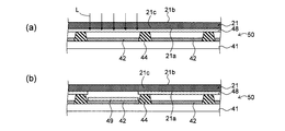
- FIG. 2A is a plan view showing an example of a layout of auxiliary electrodes, protrusions, and organic semiconductor layers of the organic semiconductor element shown in FIG.
- FIG. 2B is a plan view showing another example of the layout of the auxiliary electrode, the protrusion, and the organic semiconductor layer of the organic semiconductor element shown in FIG. 1.
- FIG. 2C is a plan view showing an example of a portion to be removed from the organic semiconductor layer on the auxiliary electrode.
- FIG. 2D is a plan view showing an example of a portion to be removed from the organic semiconductor layer on the auxiliary electrode.
- FIG. 3 is a diagram showing an element manufacturing apparatus according to the embodiment of the present invention.
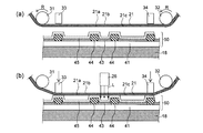
- FIGS. 4 (a) to 4 (g) are diagrams showing a device manufacturing method according to an embodiment of the present invention.
- FIG. 5 is a view showing an intermediate product processing apparatus for removing the organic semiconductor layer on the auxiliary electrode.
- FIG. 6 is a diagram illustrating a state in which the organic semiconductor layer on the auxiliary electrode is removed by using the intermediate product processing apparatus illustrated in FIG. 5.
- FIGS. 7A to 7G are views showing a method for removing an organic semiconductor layer on an auxiliary electrode in a modification of the embodiment of the present invention.
- FIGS. 8A and 8B are diagrams illustrating an example in which the intermediate product processing apparatus is used to deposit a deposition material on a substrate.
- FIG. 9 is a view showing a modification of the stage of the intermediate product processing apparatus.
- FIG. 10 is a view showing a modification of the lid member.
- FIG. 11 is a diagram illustrating a state in which the intermediate product is covered with the lid member illustrated in FIG. 10.
- FIG. 12 is a diagram illustrating an example in which the sealing mechanism includes an intermediate film.
- FIGS. 13A and 13B are diagrams illustrating an example in which a lid member is stretched between a pair of stretch members that are movable toward an intermediate product. 14A and 14B show examples in which light is irradiated from the base material side toward the organic semiconductor layer.
- FIGS. 1 to 6 In the drawings attached to the present specification, for the sake of illustration and ease of understanding, the scale, the vertical / horizontal dimension ratio, and the like are appropriately changed and exaggerated from those of the actual product.
- the layer configuration of the organic semiconductor element 40 in the present embodiment will be described with reference to FIG.
- a top emission type organic EL element will be described as an example of the organic semiconductor element 40.
- the organic semiconductor element 40 includes a base material 41, a plurality of first electrodes 42 provided on the base material 41, auxiliary electrodes 43 and protrusions provided between the first electrodes 42. A portion 44, an organic semiconductor layer 45 provided on the first electrode 42, and a second electrode 46 provided on the organic semiconductor layer 45 and the auxiliary electrode 43.
- the organic semiconductor layer 45 includes at least a light emitting layer that emits light by recombination of electrons and holes in the organic compound.
- the organic semiconductor layer 45 may further include various layers generally provided in the organic EL element, such as a hole injection layer, a hole transport layer, an electron transport layer, or an electron injection layer.
- a hole injection layer such as a hole injection layer, a hole transport layer, an electron transport layer, or an electron injection layer.
- the first electrode 42 is provided corresponding to each of the organic semiconductor layers 45.
- the first electrode 42 also functions as a reflective electrode that reflects light generated in the organic semiconductor layer 45.
- Examples of the material constituting the first electrode 42 include simple elements of metal elements such as aluminum, chromium, titanium, iron, cobalt, nickel, molybdenum, copper, tantalum, tungsten, platinum, gold, and silver, or alloys thereof. it can.
- the second electrode 46 functions as a common electrode for the plurality of organic semiconductor layers 45.
- the second electrode 46 is configured to transmit light generated in the organic semiconductor layer 45.
- a material constituting the second electrode 46 a metal film thinned to such an extent that light can be transmitted, or an oxide conductive material such as ITO can be used.
- the auxiliary electrode 43 prevents a variation in voltage drop due to a difference in distance from a power source (not shown) to each organic semiconductor layer, thereby suppressing a variation in luminance of a display device using an organic EL element. Is to do. As shown in FIG. 1, each auxiliary electrode 43 is connected to the second electrode 46. Examples of the material constituting the auxiliary electrode 43 include a single element or alloy of the same metal element as that of the first electrode 42. The auxiliary electrode 43 may be made of the same material as the first electrode 42, or may be made of a material different from the first electrode 42.
- the protrusion 44 is made of an insulating material.
- the protrusion 44 is provided between the first electrode 42 and the auxiliary electrode 43.
- the shape of the organic semiconductor layer 45 provided between the protrusions 44 can be appropriately determined.
- a material constituting the protruding portion 44 an organic material such as polyimide or an inorganic insulating material such as silicon oxide can be used.
- the protruding portion 44 is configured to extend along the normal direction of the base material 41. Therefore, when the lid material described later is brought into close contact with the base material 41, a space is provided between the lid material and the base material 41. It can also function as a spacer for ensuring the above.
- the organic semiconductor layer 45 and the second electrode 46 may be continuously provided not only on the first electrode 42 but also on the protrusion 44.
- the organic semiconductor layer 45 emits light when current flows between the first electrode 42 and the second electrode 46.
- the organic semiconductor layer 45 located on the protrusion 44 the organic semiconductor layer 45 is positioned between the first electrode 42 and the second electrode 46. No light emission occurs. 2A and 2B to be described later, the portion of the organic semiconductor layer 45 that emits light, that is, the organic semiconductor layer 45 provided on the first electrode 42 is shown.
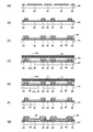
- FIG. 2A is a plan view illustrating an example of the layout of the auxiliary electrode 43, the protrusion 44, and the organic semiconductor layer 45.
- the organic semiconductor layer 45 may include a red organic semiconductor layer 45R, a green organic semiconductor layer 45G, and a blue organic semiconductor layer 45B that are arranged in order in a matrix and each have a rectangular shape.
- each of the red organic semiconductor layer 45R, the green organic semiconductor layer 45G, and the blue organic semiconductor layer 45B constitutes a sub-pixel.
- a combination of adjacent organic semiconductor layers 45R, 45G, and 45B constitutes one pixel.
- the auxiliary electrodes 43 are arranged in a grid so as to extend between the organic semiconductor layers 45 arranged in a matrix.
- the protrusion 44 is provided between the organic semiconductor layer 45 and the auxiliary electrode 43 so as to surround the organic semiconductor layer 45 provided on the first electrode 42 from the side. That is, the protrusions 44 are continuously provided along the four sides of the organic semiconductor layer 45 provided on the first electrode 42. Accordingly, it is possible to prevent the scattered organic semiconductor material from reaching the organic semiconductor layer 45 on the first electrode 42 in the step of removing the organic semiconductor layer 45 on the auxiliary electrode 43.
- the auxiliary electrode 43 does not need to be connected to the second electrode 46 over the entire area. That is, it is not necessary to remove all of the organic semiconductor layer 45 on the auxiliary electrode 43 in the removing step described later. Therefore, as shown in FIG. 2B, the protrusions 44 may be provided discontinuously along any of the four sides of the organic semiconductor layer 45. Also in the example shown in FIG. 2B, in the step of removing the organic semiconductor layer 45 on the auxiliary electrode 43 at the position sandwiched by the protrusions 44, the scattered organic semiconductor material is sandwiched at least partially by the protrusions 44. It is possible to prevent reaching the organic semiconductor layer 45 on the first electrode 42 located in the region. Further, by connecting the auxiliary electrode 43 located between the protrusions 44 to the second electrode 46, the voltage drop can be appropriately suppressed.
- the auxiliary electrode 43 is not particularly limited as long as the voltage drop of the second electrode 46 can be appropriately suppressed.
- the auxiliary electrode 43 may be provided along each pixel configured by organic semiconductor layers 45R, 45G, 45B, and 45W corresponding to a plurality of subpixels. That is, the auxiliary electrode 43 is not formed between the organic semiconductor layers 45R, 45G, 45B, and 45W, which are sub-pixels, and one pixel constituted by the organic semiconductor layers 45R, 45G, 45B, and 45W and the other similar ones.
- An auxiliary electrode 43 may be formed between these pixels.
- 2C and 2D show an example in which each pixel further includes a white organic semiconductor layer 45W in addition to the red organic semiconductor layer 45R, the green organic semiconductor layer 45G, and the blue organic semiconductor layer 45B as sub-pixels. ing.
- the arrangement of the location where the auxiliary electrode 43 and the second electrode 46 are connected is not particularly limited.
- the location where the auxiliary electrode 43 and the second electrode 46 are connected is indicated by a dotted line denoted by reference numeral 43x.
- the auxiliary electrode 43 and the second electrode 46 may be discretely connected at a plurality of locations. That is, the organic semiconductor layer 45 on the auxiliary electrode 43 may be discretely removed at a plurality of locations.
- the auxiliary electrode 43 and the second electrode 46 may be connected in a line along the direction in which the auxiliary electrode 43 extends.
- the organic semiconductor layer 45 on the auxiliary electrode 43 may be linearly removed along the direction in which the auxiliary electrode 43 extends.
- FIG. 2D shows an example in which the organic semiconductor layer 45 on the auxiliary electrode 43 is linearly removed along the direction D1 in which the lid member 21 described later is conveyed.
- 2A to 2D show examples in which a plurality of types of organic semiconductor layers 45R, 45G, 45B, and 45W are used as the organic semiconductor layer 45, the present invention is not limited to this.
- all of the organic semiconductor layers 45 constituting the sub-pixels may be configured to generate common white light.
- a color filter or the like can be used as means for color-coding each sub-pixel.
- the environment in which the element manufacturing method is implemented is not particularly limited.
- the element manufacturing method is partially under a vacuum environment.
- the specific pressure in the vacuum environment is not particularly limited as long as the pressure is lower than the atmospheric pressure.
- the internal pressure of the element manufacturing apparatus 10 is 1.0 ⁇ 10 4 Pa or less. It has become.
- FIG. 3 is a diagram schematically showing the element manufacturing apparatus 10.
- the element manufacturing apparatus 10 includes a first electrode forming apparatus 11 that forms a plurality of first electrodes 42 on a base material 41, and an auxiliary electrode formation that forms an auxiliary electrode 43 between the first electrodes 42.
- the device 12, the protrusion forming device 13 that forms the protrusion 44 between the first electrode 42 and the auxiliary electrode 43, and the organic semiconductor layer 45 is formed on the first electrode 42, the auxiliary electrode 43, and the protrusion 44.
- an organic semiconductor layer forming apparatus 14 In the following description, what is obtained by a process using each device 11, 12, 13, 14 may be referred to as an intermediate product 50.
- the element manufacturing apparatus 10 further includes an intermediate product processing apparatus 15 that performs a predetermined process while a lid material described later is in close contact with a part of the intermediate product 50.
- an example in which the intermediate product processing apparatus 15 is configured as a removing apparatus that removes the organic semiconductor layer 45 provided on the auxiliary electrode 43 will be described.
- the intermediate product processing apparatus 15 includes a stage 18, a lid material supply mechanism 20, a sealing mechanism 30, and an irradiation mechanism 25. Each component of the intermediate product processing apparatus 15 will be described later.
- the lid member 21 or the element manufacturing apparatus 10 further includes a second electrode type device 16 that forms the second electrode 46 on the auxiliary electrode 43 and the organic semiconductor layer 45 after the organic semiconductor layer 45 on the auxiliary electrode 43 is removed. ing.
- the element manufacturing apparatus 10 includes a transfer device 17 connected to each of the devices 11 to 16 in order to transfer the base material 41 and the intermediate product 50 between the devices 11 to 16 while maintaining a vacuum environment. May be further provided.
- FIG. 3 classifies each device from a functional viewpoint, and the physical form is not limited to the example shown in FIG.
- a plurality of devices among the devices 11 to 16 shown in FIG. 3 may be physically constituted by one device.
- any of the devices 11 to 16 shown in FIG. 3 may be physically configured by a plurality of devices.
- the first electrode 42 and the auxiliary electrode 43 may be formed simultaneously in one process.
- the first electrode forming device 11 and the auxiliary electrode forming device 12 may be configured as one device.
- a method for manufacturing the organic semiconductor element 40 using the element manufacturing apparatus 10 will be described.
- a metal material layer constituting the first electrode 42 and the auxiliary electrode 43 is formed on the substrate 41 by, for example, a sputtering method, and then the metal material layer is formed by etching.
- the first electrode 42 and the auxiliary electrode 43 described above can be simultaneously formed on the base material 41.
- the step of forming the first electrode 42 and the step of forming the auxiliary electrode 43 may be performed separately.
- the normal line of the base material 41 is interposed between the first electrode 42 and the auxiliary electrode 43 and above the first electrode 42 and the auxiliary electrode 43 by, for example, photolithography.
- a plurality of protrusions 44 extending in the direction are formed.
- a general film forming method such as a vapor deposition method, a CVD method, a printing method, an ink jet method, or a transfer method, the first electrode 42, the auxiliary electrode 43, and the protrusion 44
- An organic semiconductor layer 45 is formed thereon.
- An intermediate product 50 including the organic semiconductor layer 45 provided on the electrode 43 and the protrusion 44 can be obtained.
- the first electrode 42 and the auxiliary electrode 43 are formed on the base material 41 before the protrusion 44. For this reason, the first electrode 42 and the auxiliary electrode 43 are partially covered by the protrusion 44.
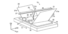
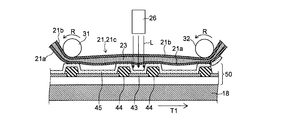
- the lid member 21 is prepared, and then the first surface 21a of the lid member 21 is brought into close contact with a part of the intermediate product 50 as shown in FIG.
- the organic semiconductor layer 45 provided on the auxiliary electrode 43 is irradiated with light L such as laser light, as shown in FIG. .
- the energy of the light L is absorbed by the organic semiconductor layer 45, and as a result, the organic semiconductor material constituting the organic semiconductor layer 45 on the auxiliary electrode 43 is scattered. In this way, the organic semiconductor layer 45 on the auxiliary electrode 43 can be removed.
- the organic semiconductor material scattered from the auxiliary electrode 43 adheres to the first surface 21a of the lid member 21, for example, as shown in FIG.
- FIG. 4F is a diagram showing a state where the organic semiconductor layer 45 on the auxiliary electrode 43 has been removed.
- the second electrode 46 is formed on the organic semiconductor layer 45 on the first electrode 42 and on the auxiliary electrode 43.
- the organic semiconductor element 40 including the auxiliary electrode 43 connected to the second electrode 46 can be obtained.
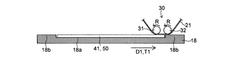
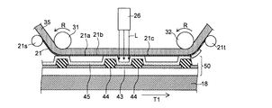
- FIG. 5 the method for bringing the lid material 21 into close contact with a part of the intermediate product 50 and removing the organic semiconductor layer 45 on the auxiliary electrode 43 described with reference to FIGS. This will be described in more detail with reference to FIG. Note that the steps shown in FIGS. 4D and 4E are performed by the intermediate product processing apparatus 15 described above. First, the configuration of the intermediate product processing apparatus 15 will be described in detail with reference to FIG. In FIG. 5, the first direction, the second direction, and the third direction orthogonal to each other are indicated by arrows D1, D2, and D3, respectively.
- the intermediate product processing apparatus 15 includes a stage 18 on which the intermediate product 50 is placed, a lid material supply mechanism 20 that supplies a long lid material 21, and a part of the lid material 21.
- a sealing mechanism 30 that is in close contact with a part of the intermediate product 50 and an irradiation mechanism 25 that irradiates light to a portion of the intermediate product 50 where the lid member 21 is in close contact are provided.
- Each component of the intermediate product processing apparatus 15 is disposed in a chamber maintained in a vacuum atmosphere. For this reason, the process of removing the organic semiconductor layer 45 on the auxiliary electrode 43 can be performed in a vacuum environment.
- “long” means that the size of the lid 21 in the direction in which the lid 21 is conveyed is at least five times the dimension of the lid 21 in the direction perpendicular to the direction in which the lid 21 is conveyed. It means that
- stage 18 The stage 18 has a mounting surface 18a for supporting the intermediate product 50, and the mounting surface 18a extends in parallel with the first direction D1 and the second direction D2.
- the stage 18 is configured to be movable in a stage moving direction T1 parallel to the first direction D1.
- the intermediate product 50 is placed on the stage 18 so that the plurality of protrusions 44 described above are arranged on the base material 41 along the first direction D1. For this reason, as will be described later, by repeating the movement of the stage 18 along the stage moving direction T1 and the irradiation mechanism 25 irradiating the light toward the intermediate product 50, the first of the intermediate products 50.
- the protrusion 44 of the intermediate product 50 placed on the stage 18 extends along a third direction D3 orthogonal to the first direction D1 and the second direction D2.
- the sealing mechanism 30 includes a pair of rollers 31 and 32 that rotate in a rotation direction R around a rotation axis that extends in a second direction D2 orthogonal to the first direction D1.
- the pair of rollers 31 and 32 includes a first roller 31 and a second roller 32.
- the lid supply mechanism 20 is not shown, but the feeding portion that feeds the lid 21 along the feeding direction T2 between the first roller 31 and the intermediate product 50, the second roller 32, and the intermediate product. And a winding portion that winds the lid member 21 after passing through 50 along the winding direction T3.
- the lid member 21 for covering a part of the intermediate product 50 is supplied in a roll-to-roll manner.
- a surface facing the stage 18 side of the surface of the lid member 21 is referred to as a first surface 21a
- a surface on the opposite side of the first surface 21a is referred to as a second surface 21b.
- Each of the rollers 31 and 32 is in contact with the second surface 21b of the lid member 21.
- PET polyethylene terephthalate
- COP cycloolefin polymer
- PP polypropylene
- PE polyethylene
- PC polycarbonate
- the rollers 31 and 32 of the sealing mechanism 30 are configured to rotate in synchronization with the movement of the stage 18. That is, each roller 31 and 32 conveys the cover material 21 wound around each roller 31 and 32 so that the moving speed of the stage 18 and the conveyance speed of the cover material 21 coincide.
- Each of the rollers 31 and 32 is configured not only to transport the lid member 21 but also to apply a predetermined tension to the lid member 21 positioned between the first roller 31 and the second roller 32. Yes. For this reason, it can be said that the part located between the 1st roller 31 and the 2nd roller 32 among the cover materials 21 exists in the state stretched by a pair of rollers 31 and 32.
- a portion of the lid member 21 that is stretched between the pair of rollers 31 and 32 is also referred to as a stretched portion 21c.
- each of the pair of rollers 31 and 32 is provided with a drive unit for supporting and rotating the rollers 31 and 32 at predetermined positions.
- the specific configuration of the drive unit for rotating the rollers 31 and 32 is not particularly limited.
- the irradiation mechanism 25 has an optical head 26 that emits light L such as laser light. The light emitted from the optical head 26 passes through the stretched portion 21 c of the lid member 21 and reaches the intermediate product 50.
- the irradiation mechanism 25 may further include a lens for focusing the light L with respect to the organic semiconductor layer 45.
- the optical head 26 is fixed with respect to the movement of the stage 18 and the rotation of the roller 31. That is, they are arranged independently from the stage 18 and the roller 31.
- the optical head 26 is configured so that the traveling direction of the light L generated by the optical head 26 does not change even if the stage 18 moves or the roller 31 rotates.
- the stage 18 is movable in the first direction D1, and the protrusions 44 of the intermediate product 50 are arranged along the first direction D1. Therefore, even when the optical head 26 is in a stationary state, it is possible to sequentially irradiate the plurality of protrusions 44 or their peripheral portions with light.
- the aim of the optical head 26 is not shifted during the process. Accordingly, it is possible to irradiate light with higher positional accuracy than when irradiating light to a plurality of portions of the intermediate product 50 while moving the optical head 26.
- the optical head 26 may be configured to be movable in the second direction D2, that is, in the direction along the rotation axis of each of the rollers 31 and 32, as indicated by an arrow M in FIG. This makes it possible to irradiate an arbitrary part of the intermediate product 50 with light, as will be described later.
- a specific configuration for moving the optical head 26 is not particularly limited.
- the optical head 26 can move along a rail 27 disposed above the stage 18.
- the second direction is used when the optical head 26 is configured to be able to selectively extract light at an arbitrary position in the second direction. It becomes possible to irradiate the light toward the intermediate product 50 at any position.
- a mask in which a plurality of openings are formed is disposed between the irradiation mechanism 25 and the lid member 21, and A method of selectively shielding the opening of the mask is conceivable.
- the portion of the intermediate product 50 that is to be irradiated with light is along the first direction orthogonal to the second direction. It does not have to be lined up. Accordingly, although not shown, the protrusions 44 of the intermediate product 50 do not have to be arranged along the first direction D1.
- the lid member 21 having the first surface 21 a is prepared so that the first surface 21 a faces the protruding portion 44 side of the intermediate product 50.
- a lid material supply step of supplying the lid material 21 between the first roller 31 and the intermediate product 50 so that the first surface 21 a of the lid material 21 faces the stage 18 side is performed.
- a sealing step of pressing a part of the first surface 21 a of the lid member 21 against the intermediate product 50 using the pair of rollers 31 and 32 of the sealing mechanism 30 is performed. Thereby, a part of the first surface 21 a of the lid member 21 is in close contact with a part of the intermediate product 50. Specifically, as shown in FIG.
- the first surface 21 a of the stretched portion 21 c of the lid member 21 is in close contact with a part of the intermediate product 50.
- a predetermined tension is applied to the stretched portion 21 c of the lid member 21 stretched between the pair of rollers 31 and 32.
- abuts to a pair of rollers 31 and 32 among the cover materials 21 is each pressed toward the intermediate product 50, as shown in FIG.
- the tension part 21c between a pair of rollers 31 and 32 is pressed with respect to the intermediate product 50 with predetermined pressure. It is in the state where it was done. For example, in the example illustrated in FIG.
- the stretched portion 21 c is pressed against the portion of the intermediate product 50 where the protrusion 44 is provided with a predetermined pressure. Therefore, the first surface 21a of the lid member 21 can be closely attached to the portion of the intermediate product 50 where the protrusion 44 is provided without any gap.
- an irradiation step of irradiating the intermediate product 50 with light through the lid member 21 is performed on a portion of the intermediate product 50 that is in close contact with the lid member 21.
- the “part in close contact with the lid member 21” means not only the portion of the protrusion 44 that is in direct contact with the first surface 21 a of the lid member 21 but also the first surface 21 a of the lid member 21. This is a concept including a portion surrounded by the protruding portion 44. Note that it is not necessary to irradiate all the portions of the intermediate product 50 that are in close contact with the lid member 21.
- the light is irradiated to a portion of the intermediate product 50 that is in close contact with the lid member 21 and that is provided with the organic semiconductor layer 45 to be removed.
- the organic semiconductor layer 45 absorbs the energy of the light L, the organic semiconductor material constituting the organic semiconductor layer 45 on the auxiliary electrode 43 is scattered as described above.
- the stretched portion 21c that is tensioned with a predetermined tension is formed on the lid member 21, and this stretched portion 21c is intermediate product with a predetermined pressure. It is pressed against a part of 50. For this reason, the 1st surface 21a of the stretch part 21c of the cover material 21 can be closely_contact
- the organic semiconductor element 40 having high quality can be manufactured at a low cost.
- the organic semiconductor layer 45 on the auxiliary electrode 43 is removed, the light from the irradiation mechanism 25 is stopped. That is, the light irradiation to the intermediate product 50 is stopped.
- the stage 18 is moved along the stage moving direction T1, and the lid member 21 is moved along the rotation direction R of the rollers 31 and 32.
- the irradiation mechanism 25 emits light again.
- the light L from the irradiation mechanism 25 is again irradiated to the organic semiconductor layer 45 on the auxiliary electrode 43, and thereby the organic semiconductor layer 45 is removed.
- the organic semiconductor layers 45 on the plurality of auxiliary electrodes 43 arranged along the first direction D1 parallel to the stage moving direction T1 can be sequentially removed.
- the organic semiconductor layers 45 on the auxiliary electrode 43 are arranged at equal intervals on the base material 41. Accordingly, light emission from the irradiation mechanism 25 is turned on and off at a constant cycle considering the interval between the auxiliary electrodes 43 and the moving speed of the stage 18, and thereby the organic semiconductor layer 45 on the auxiliary electrode 43 is sequentially irradiated with light. May be.
- the optical head 26 of the irradiation mechanism 25 remains stationary as described above. For this reason, according to the present embodiment, it is possible to irradiate light to the intermediate product 50 with high positional accuracy, and thereby, the organic semiconductor layer 45 of the auxiliary electrode 43 can be accurately removed.
- the intermediate product 50 on the moving stage 18 it is possible to cover the intermediate product 50 on the moving stage 18 by using the lid 21 supplied in a roll-to-roll manner. For this reason, the above-mentioned process of removing the organic semiconductor layer 45 on the auxiliary electrode 43 can be performed on the plurality of intermediate products 50 using one roll body around which the lid member 21 is wound. Therefore, an apparatus or process for cutting the lid member 21 for each intermediate product 50 is not necessary, and therefore the apparatus configuration and process can be simplified. Moreover, the waste resulting from the cutting
- the rail 27 The optical head 26 may be moved along After the optical head 26 is moved, the organic semiconductor layer 45 on the plurality of auxiliary electrodes 43 positioned on a new line can be removed by performing the above-described process again while moving the stage 18.
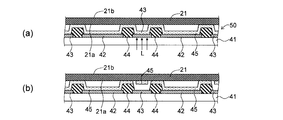
- a plurality of protrusions 44 are formed on the base material 41.
- the first electrode 42 is formed between the protrusions 44, and the auxiliary electrode 43 is formed on the protrusions 44.
- a plurality of first electrodes 42 insulated from each other by the protrusions 44 and the auxiliary electrodes 43 provided on the protrusions 44 can be obtained.
- the first electrode 42 is formed on the base material 41, then the projection 44 is formed between the first electrodes 42, and then the auxiliary electrode 43 is formed on the projection 44. May be. Thereafter, as shown in FIG.
- an organic semiconductor layer 45 is formed on the first electrode 42, the auxiliary electrode 43, and the protrusion 44.
- the base material 41, the plurality of first electrodes 42 provided on the base material 41, the auxiliary electrode 43 and the protrusion 44 provided between the first electrodes 42, the first electrode 42 and the auxiliary An intermediate product 50 including the organic semiconductor layer 45 provided on the electrode 43 can be obtained.
- the protrusion 44 is formed before the auxiliary electrode 43, so that the protrusion 44 is covered with the auxiliary electrode 43.
- the protrusion 44 does not need to be covered with the auxiliary electrode 43 over the entire upper surface. That is, the upper surface of the protrusion 44 only needs to be at least partially covered by the auxiliary electrode 43.
- the example in which the protrusions 44 are provided in two rows between the first electrodes 42 and the auxiliary electrode 43 is provided between the protrusions 44 has been described. Since the electrodes 43 are provided on the protrusions 44, the protrusions 44 provided between the first electrodes 42 may be in only one row as shown in FIG.
- the stretched portion 21 c of the lid member 21 is pressed against a part of the intermediate product 50 using a pair of rollers 31 and 32 of the sealing mechanism 30, whereby the lid member A lid material adhesion process is performed in which a part of the first surface 21 a of 21 is adhered to a part of the intermediate product 50.
- the stage 18 on which the intermediate product 50 is placed is omitted.
- portions of the lid member 21 that are in contact with the pair of rollers 31 and 32 are each pressed toward the intermediate product 50. For this reason, not only the part which contact
- FIG. 7F is a diagram showing a state where the organic semiconductor layer 45 on the auxiliary electrode 43 on the protrusion 44 is removed.
- the lid member 21 is in close contact with the organic semiconductor layer 45 to be removed.
- the organic semiconductor layer 45 on the auxiliary electrode 43 on the protruding portion 44 can be attached to the first layer 21 of the lid member 21 without irradiating the light L. It is also possible to transfer to the first surface 21a. That is, it is possible to remove the organic semiconductor layer 45 provided on the auxiliary electrode 43 by closely attaching the stretched portion 21 c of the lid member 21 to a part of the intermediate product 50.
- the second electrode 46 is formed on the organic semiconductor layer 45 on the first electrode 42 and on the auxiliary electrode 43 on the protrusion 44.
- the organic semiconductor element 40 including the auxiliary electrode 43 connected to the second electrode 46 can be obtained.
- the intermediate product processing apparatus 15 is configured as an exposure apparatus
- the example in which the intermediate product processing apparatus 15 is used as a removing apparatus that removes the organic semiconductor layer 45 on the auxiliary electrode 43 is shown.
- the application example of the intermediate product processing apparatus 15 is not particularly limited.
- the intermediate product processing apparatus 15 performs an exposure process of irradiating the exposure layer in the intermediate product 50 with light L as exposure light while the lid 21 is in close contact with the intermediate product 50. It may be used as an exposure apparatus.
- the intermediate product processing apparatus 15 irradiates the vapor deposition material 48 with light while the lid 21 is in close contact with the intermediate product 50, and the vapor deposition material 48. May be used as a vapor deposition apparatus for vapor-depositing the material on the substrate 41.
- the vapor deposition material 48 is provided on the first surface 21a of the lid member 21 as shown in FIG. 8A
- the intermediate product 50 includes a base material 41, a plurality of protrusions 44 provided on the base material 41, a first electrode 42 provided between the protrusions 44, have.
- the vapor deposition material 48 evaporates. More specifically, as shown in FIG. 8A, when the vapor deposition material 48 existing at a position facing the first electrode 42 in the vapor deposition material 48 is irradiated with light L, the vapor deposition material 48 evaporates.
- a vapor deposition layer 49 can be formed on the first electrode 42 as shown in FIG. Further, the space between the base material 41 and the lid member 21 is appropriately partitioned by the protrusions 44. For this reason, it is possible to prevent the vapor deposition material 48 from being scattered over a wide area in the space between the base material 41 and the lid member 21.
- the method of heating and evaporating the vapor deposition material 48 is not limited to the above.
- a metal thin film that absorbs infrared light is formed between the first surface 21a of the lid member 21 and the organic semiconductor layer 45, and the metal thin film is irradiated with light to heat the metal thin film, thereby vapor deposition.
- the material 48 may be heated.
- the vapor deposition material 48 provided on the first surface 21a of the lid member 21 is hardly directly irradiated with light, but the vapor deposition material 48 can be indirectly heated through the metal thin film. Therefore, the vapor deposition material 48 can be evaporated.
- a magnetic field is generated around the lid member 21 or the lid member 21 of the intermediate product 50 is generated in order to further increase the degree of adhesion of the lid member 21 to the intermediate product 50.
- a magnetic material may be disposed on the opposite side of the lid member 21 so that the lid member 21 is drawn toward the intermediate product 50 by a magnetic force.
- the stage 18 on which the intermediate product 50 is placed protrudes in the normal direction of the base material 41 so as to be adjacent to the end of the base material 41 of the intermediate product 50 in the first direction D1.
- Region 18b may be formed.
- the protruding region 18 b is configured such that the position of the upper surface thereof substantially coincides with the position of the upper surface of the intermediate product 50.
- the pair of rollers 31 and 32 is configured such that one roller, for example, the first roller 31 is positioned on the intermediate product 50 via the lid member 21, and the other roller, for example, the second roller 32 is disposed via the lid member 21.
- the lid member 21 can be stretched while being positioned on the protruding region 18 b of the stage 18.
- the stretched portion 21 c of the lid member 21 can be positioned in the vicinity of the end portion of the base material 41 of the intermediate product 50. This makes it possible to closely attach the stretched portion 21 c of the lid member 21 to a portion of the intermediate product 50 in the vicinity of the end portion of the base material 41. Therefore, the process using the intermediate product processing apparatus 15 can be performed on the entire area of the intermediate product 50.
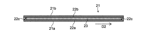
- the lid member 21 is configured by a single layer made of a light-transmitting material.
- the lid member 21 may be composed of a plurality of layers.
- the lid member 21 may include a first film 22a and a second film 22b.
- the first film 22a constitutes the first surface 21a of the lid member 21 facing the stage 18 side
- the second film 22b constitutes the second surface 21b on the opposite side of the first surface 21a.
- FIG. 10 is a cross-sectional view showing the case where the lid member 21 is cut along the second direction D2 described above, that is, along the direction of the rotation axis of the rollers 31 and 32.
- a sealing material 22c may be interposed between the first film 22a and the second film 22b.
- the sealing material 22c extended along the length direction of each film 22a, 22b is provided in the edge part vicinity of each film 22a, 22b in the 2nd direction D2, respectively.
- a space is provided between the first film 22a and the second film 22b, and the space 23 between the first film 22a and the second film 22b is sealed from the outside. It becomes possible to do. For example, it becomes possible to enclose a gas such as air or nitrogen in the space between the first film 22a and the second film 22b. Advantages of using the lid member 21 in which the gas is sealed in the internal space 23 will be described below with reference to FIG.
- the sealing step in which the first surface 21a of the lid 21 is in close contact with a part of the intermediate product 50 is performed in a reduced pressure environment having a pressure lower than the atmospheric pressure, such as a vacuum environment.
- the gas is sealed between the first film 22a and the second film 22b
- the gas is sealed in the lid member 21 based on the difference between the pressure of the gas and the pressure under the reduced pressure environment.
- the gas expands.
- the interval between the first film 22a and the second film 22b tends to increase. That is, the films 22a and 22b try to swell outward.
- the distance between the first film 22 a and the second film 22 b is the distance between the intermediate product 50 and the rollers 31 and 32.
- the first film 22 a is intermediate based on the gas expansion.
- the product 50 swells toward a space where the protruding portion 44 does not exist. This means that the first film 22a is more closely attached to the portion of the intermediate product 50 where the protrusions 44 are provided, compared to the case where such swelling does not occur.
- the first surface 21a of the lid member 21 constituted by the first film 22a can be brought into close contact with the portion of the intermediate product 50 where the protrusions 44 are provided without any gaps. It becomes like this. This can more reliably prevent the organic semiconductor material scattered from the auxiliary electrode 43 from contaminating the organic semiconductor layer 45 on the first electrode 42 and the surrounding environment.
- the specific structure of the cover material 21 is not specifically limited.
- a hollow resin having a large number of hollow portions may be provided between the first film 22a and the second film 22b.
- a gas such as air is present in the hollow portion of the hollow resin. Therefore, when the lid 21 provided with the hollow resin is placed in a vacuum environment, the gas in the hollow portion of the hollow resin expands, As a result, the films 22a and 22b swell outward. Further, by providing the hollow resin, the interval between the first film 22a and the second film 22b can be stably maintained.
- the hollow resin for example, a resin containing hollow particles made of styrene, acrylic, silica, or the like, or a resin having a hollow structure such as porous silica can be used.
- the sealing mechanism 30 may have an intermediate film provided between the pair of rollers 31 and 32 and the lid member 21.
- the long intermediate film unwound from the unillustrated unwinding section is conveyed along the pair of rollers 31 and 32 and then wound by the unillustrated winding section. Yes.
- the pair of rollers 31 and 32 press the lid 21 toward the intermediate product 50 through the intermediate film 35. Therefore, also in this modification, as in the case of the above-described embodiment, the stretched portion 21c between the pair of rollers 31 and 32 of the lid member 21 is connected to the intermediate product 50 via the intermediate film 35. And pressed at a predetermined pressure. Therefore, the first surface 21a of the lid member 21 can be closely attached to the portion of the intermediate product 50 where the protrusion 44 is provided without any gap.
- the pressing force and tension received by the lid member 21 are not directly applied to the lid member 21 from the pair of rollers 31 and 32 but are applied to the lid member 21 via the intermediate film 35.
- the intermediate film 35 is in contact with the lid member 21 over a wide area at a portion located between the pair of rollers 31 and 32.
- deformation transformation, such as a wrinkle, arises in the cover material 21 resulting from the pressing force and tension
- the lid member 21 unwound from the unwinding portion 21s covers the intermediate product 50 in a state of being overlapped with the intermediate film 35, and then is separated from the intermediate film 35 and wound by the winding portion 21t.
- the material constituting the intermediate film 35, the thickness and the layer structure of the intermediate film 35, and the like are selected so that a suitable pressing force or tension can be applied to the lid member 21 via the intermediate film 35.
- a material having a higher elastic coefficient than the material constituting the lid member 21 is used as the material constituting the intermediate film 35.
- the intermediate film 35 is curved so as to protrude toward the intermediate product 50 between the pair of rollers 31 and 32.
- the lid member 21 may be pressed more strongly against the product 50.
- the intermediate film 35 may include a pair of films and an interference layer provided between the pair of films.
- the pair of films for example, a pair of PET films each having a thickness in the range of 100 ⁇ m to 500 ⁇ m can be used.
- the gel-form material which has translucency can be used as a material which comprises an interference layer.
- an optical adhesive material having translucency so-called OCA can be used.
- the organic semiconductor material scattered from the auxiliary electrode 43 of the intermediate product 50 adheres to the first surface 21a of the lid member 21. Therefore, in order to manufacture the organic semiconductor element 40 having high quality, it is preferable that the lid member 21 to which the organic semiconductor material is attached is discarded without being reused in the manufacturing process of the organic semiconductor element 40. On the other hand, the organic semiconductor material does not adhere to the intermediate film 35. Moreover, as shown in FIG. 12, the cover material 21 and the intermediate film are separated and collected separately. Therefore, it is possible to reuse the intermediate film 35 in the manufacturing process of the organic semiconductor element 40 performed thereafter.
- a pair of rollers 31 and 32 are used as a pair of stretching members for applying tension to the lid member 21.
- the specific configuration of the pair of stretching members is not particularly limited as long as tension can be applied to the portion of the lid member 21 that covers the intermediate product 50.
- the pair of stretching members 33 and 34 of the sealing mechanism 30 can move toward the intermediate product 50 so as to press the lid 21 toward the intermediate product 50.
- It may be a pair of members configured as described above.
- the lid member 21 is conveyed by the pair of rollers 31 and 32 when the stretching members 33 and 34 are not in contact with the second surface 21 b of the lid member 21. Is done.
- FIG. 13 (b) in a state where the pair of rollers 31, 32 are stopped, the pair of stretching members 33, 34 are moved toward the intermediate product 50, and the pair of stretching members 33, 34 is brought into contact with the second surface 21 b of the lid member 21.
- the auxiliary electrode 43 is generally composed of a single metal element or an alloy.
- the light L emitted toward the lid member 21 that is in close contact with the intermediate product 50 is mainly shielded by the auxiliary electrode 43.
- light having a wavelength that can be absorbed by the auxiliary electrode 43 is used as the light L, whereby the auxiliary electrode 43 can be heated and thereby the organic semiconductor layer 45 on the auxiliary electrode 43 can be heated.
- the organic semiconductor layer 45 on the auxiliary electrode 43 can be evaporated and adhered onto the first surface 21 a of the lid member 21.
- a material that can absorb the light L may be used as the material constituting the auxiliary electrode 43.
- the stage 18 is used as a support mechanism for supporting the intermediate product 50
- the specific configuration of the support mechanism that supports the intermediate product 50 is not particularly limited as long as the intermediate product 50 can be appropriately supported when the lid 21 is brought into close contact with the intermediate product 50.
- the unwinding unit that unwinds the intermediate product 50, the winding unit that winds up the intermediate product 50, and the intermediate product 50 that is being transported are in contact with each other.
- a transport roll, a guide roll, or the like may function as a support mechanism that supports the intermediate product 50.
- the base material 41 of the intermediate product 50 extends in a long shape, and the first electrode 42 and the auxiliary electrode 43 of the intermediate product 50 are also provided.
- the projecting portion 44, the organic semiconductor layer 45, the second electrode 46, and the like are formed on a base material 41 extending in a long shape.
- the organic semiconductor element 40 is an organic EL
- the type of the organic semiconductor element manufactured by the above-described element manufacturing apparatus 10 and the element manufacturing method is not particularly limited.
- organic transistor device known organic semiconductor layers and other components can be used, for example, those described in JP-A-2009-87996.
- organic solar cell device known photoelectric conversion layers composed of organic semiconductor layers and other components can be used, for example, those described in JP2011-151195A Can do.
- the element manufacturing apparatus 10 and the element manufacturing method described above may be applied not only to the manufacture of organic semiconductor elements but also to the manufacture of inorganic semiconductor elements.
- each component of the intermediate product processing apparatus 15 is disposed in a chamber maintained in a vacuum atmosphere. That is, the example in which the step of irradiating the intermediate product 50 with light using the intermediate product processing apparatus 15 is performed in a vacuum environment is shown.
- the present invention is not limited to this, and the step of irradiating the intermediate product 50 with light using the intermediate product processing apparatus 15 may be performed under an environment other than the vacuum environment such as an atmospheric pressure environment.
Landscapes
- Engineering & Computer Science (AREA)
- Physics & Mathematics (AREA)
- Optics & Photonics (AREA)
- Plasma & Fusion (AREA)
- Mechanical Engineering (AREA)
- Manufacturing & Machinery (AREA)
- Electroluminescent Light Sources (AREA)
- High Energy & Nuclear Physics (AREA)
- Electromagnetism (AREA)
- Health & Medical Sciences (AREA)
- Toxicology (AREA)
- Condensed Matter Physics & Semiconductors (AREA)
- General Physics & Mathematics (AREA)
- Computer Hardware Design (AREA)
- Microelectronics & Electronic Packaging (AREA)
- Power Engineering (AREA)
Abstract
Description
図1に示すように有機半導体素子40は、基材41と、基材41上に設けられた複数の第1電極42と、第1電極42間に設けられた補助電極43および突起部44と、第1電極42上に設けられた有機半導体層45と、有機半導体層45上および補助電極43上に設けられた第2電極46と、を備えている。 As shown in FIG. 1, the
図3は、素子製造装置10を概略的に示す図である。図3に示すように、素子製造装置10は、基材41上に複数の第1電極42を形成する第1電極形成装置11と、第1電極42間に補助電極43を形成する補助電極形成装置12と、第1電極42と補助電極43との間に突起部44を形成する突起部形成装置13と、第1電極42、補助電極43上および突起部44上に有機半導体層45を形成する有機半導体層形成装置14と、を備えている。以下の説明において、各装置11,12,13,14を用いた工程によって得られるものを中間製品50と称することもある。 Element Manufacturing Apparatus FIG. 3 is a diagram schematically showing the
以下、図4(a)~(g)を参照して、素子製造装置10を用いて有機半導体素子40を製造する方法について説明する。はじめに、例えばスパッタリング法によって、第1電極42および補助電極43を構成する金属材料の層を基材41上に形成し、次に、金属材料の層をエッチングによって成形する。これによって、図4(a)に示すように、上述の第1電極42および補助電極43を同時に基材41上に形成することができる。なお、第1電極42を形成する工程および補助電極43を形成する工程は、別個に実施されてもよい。 Element Manufacturing Method Hereinafter, with reference to FIGS. 4A to 4G, a method for manufacturing the
上述の図4(d)(e)を参照して説明した、蓋材21を中間製品50の一部に密着させるとともに補助電極43上の有機半導体層45を除去する方法について、図5および図6を参照してより詳細に説明する。なお図4(d)(e)に示す工程は、上述の中間製品処理装置15によって実施される。はじめに図5を参照して、中間製品処理装置15の構成について詳細に説明する。図5においては、互いに直交する第1方向、第2方向および第3方向がそれぞれ矢印D1、D2およびD3で示されている。 (Intermediate product processing equipment)
4 and FIG. 5, the method for bringing the
ステージ18は、中間製品50を支持するための載置面18aを有しており、この載置面18aは、第1方向D1および第2方向D2に平行に広がっている。またステージ18は、第1方向D1に平行なステージ移動方向T1において移動可能であるよう構成されている。また中間製品50は、上述の複数の突起部44が第1方向D1に沿って基材41上に並ぶよう、ステージ18に載置されている。このため後述するように、ステージ18をステージ移動方向T1に沿って移動させることと、照射機構25によって中間製品50に向けて光を照射することとを繰り返すことにより、中間製品50のうち第1方向D1に沿って並ぶ複数の突起部44またはその周辺部分に対して順次光を照射することが可能になる。なおステージ18に載置されている中間製品50の突起部44は、第1方向D1および第2方向D2に直交する第3方向D3に沿って延びている。 (stage)
The
図5に示すように、封止機構30は、第1方向D1に直交する第2方向D2に延びる回転軸を中心として回転方向Rにおいて回転する一対のローラー31,32を有している。一対のローラー31,32は、第1ローラー31および第2ローラー32からなっている。一方、蓋材供給機構20は、図示はしないが、第1ローラー31と中間製品50との間に向けて繰り出し方向T2に沿って蓋材21を繰り出す繰出部と、第2ローラー32と中間製品50との間を通った後の蓋材21を巻き取り方向T3に沿って巻き取る巻取部と、を有している。このように本実施の形態においては、中間製品50の一部を覆うための蓋材21が、ロール・トゥー・ロールで供給される。以下の説明において、蓋材21の面のうちステージ18側を向く面を第1面21aと称し、第1面21aの反対側にある面を第2面21bと称する。各ローラー31,32はそれぞれ蓋材21の第2面21bに当接する。 (Cover material supply mechanism and sealing mechanism 30)
As shown in FIG. 5, the
図5に示すように、照射機構25は、レーザ光などの光Lを放射する光ヘッド26を有している。光ヘッド26から放射された光は、蓋材21の張架部分21cを透過して中間製品50に到達する。なお照射機構25は、光Lの焦点を有機半導体層45に対してあわせるためのレンズなどをさらに含んでいてもよい。 (Irradiation mechanism)
As shown in FIG. 5, the
第2方向の任意の位置で中間製品50に向けて光を照射することが可能である場合、中間製品50のうち光が照射されるべき部分は、第2方向に直交する第1方向に沿って並んでいなくてもよい。従って、図示はしないが、中間製品50の突起部44は、第1方向D1に沿って並んでいなくてもよい。 The
When light can be irradiated toward the
このように本実施の形態によれば、一対のローラー31,32という簡易な構成要素を用いて、中間製品50の一部を蓋材21によって効率良く覆うことができる。このため、高い品質を有する有機半導体素子40を低いコストで製造することができる。
補助電極43上の有機半導体層45が除去されると、照射機構25からの光は停止される。すなわち、中間製品50に対する光の照射が停止される。 Here, according to the present embodiment, as described above, the stretched
As described above, according to the present embodiment, it is possible to efficiently cover a part of the
When the
上述の本実施の形態において、第1電極42および補助電極43が突起部44よりも先に基材41上に形成される例を示した。しかしながら、これに限られることはなく、突起部44を第1電極42および補助電極43よりも先に基材41上に形成してもよい。このような場合であっても、上述した本実施の形態による密着工程や除去工程を利用することができる。以下、このような例について図7(a)~(g)を参照して説明する。 (Modification of layer structure of organic semiconductor element)
In the above-described embodiment, the example in which the
その後、図7(c)に示すように、第1電極42,補助電極43および突起部44上に有機半導体層45を形成する。このようにして、基材41と、基材41に設けられた複数の第1電極42と、第1電極42間に設けられた補助電極43および突起部44と、第1電極42上および補助電極43上に設けられた有機半導体層45と、を含む中間製品50を得ることができる。なお本変形例においては、補助電極43よりも先に突起部44が形成されるため、突起部44が補助電極43によって覆われている。なお突起部44は、その上面が全域にわたって補助電極43によって覆われている必要はない。すなわち突起部44は、その上面が少なくとも部分的に補助電極43によって覆われていればよい。また上述の本実施の形態においては、第1電極42間に2列にわたって突起部44が設けられ、突起部44間に補助電極43が設けられる例を示したが、本変形例においては、補助電極43が突起部44上に設けられるため、図7(c)に示すように第1電極42間に設けられる突起部44は1列のみであってもよい。 First, as shown in FIG. 7A, a plurality of
Thereafter, as shown in FIG. 7C, an
また上述の本実施の形態および変形例において、中間製品処理装置15が、補助電極43上の有機半導体層45を除去する除去装置として使用される例を示した。しかしながら、中間製品処理装置15の応用例が特に限られることはない。例えば中間製品処理装置15は、図示はしないが、中間製品50に蓋材21が密着されている間に中間製品50中の被露光層に対して光Lを露光光として照射する露光工程を実施する露光装置として使用されてもよい。 (Example in which the intermediate product processing apparatus is configured as an exposure apparatus)
Further, in the above-described embodiment and modification examples, the example in which the intermediate
若しくは、中間製品処理装置15は、図8(a)(b)に示すように、中間製品50に蓋材21が密着されている間に蒸着用材料48に光を照射して蒸着用材料48を基材41上に蒸着させる蒸着装置として使用されてもよい。 (Example in which the intermediate product processing device is configured as a vapor deposition device)
Alternatively, as illustrated in FIGS. 8A and 8B, the intermediate
中間製品50が載置されるステージ18には、図9に示すように、第1方向D1における中間製品50の基材41の端部に隣接するよう基材41の法線方向に突出した突出領域18bが形成されていてもよい。突出領域18bは、その上面の位置が中間製品50の上面の位置とほぼ一致するよう構成されている。この場合、一対のローラー31,32は、一方のローラー、例えば第1ローラー31が蓋材21を介して中間製品50上に位置し、他方のローラー、例えば第2ローラー32が蓋材21を介してステージ18の突出領域18b上に位置する状態で、蓋材21を張架することができるようになる。このため、蓋材21の張架部分21cを、中間製品50の基材41の端部近傍に位置づけることができるようになる。このことにより、中間製品50のうち基材41の端部近傍の部分に対して、蓋材21の張架部分21cを密着させることが可能になる。従って、中間製品50の全域に対して中間製品処理装置15を用いた処理を実施することができる。 (Stage variation)
As shown in FIG. 9, the
上述の本実施の形態および各変形例においては、蓋材21が、透光性を有する材料からなる単一の層で構成されている例を示した。しかしながら、蓋材21が複数の層から構成されていてもよい。例えば図10に示すように、蓋材21は、第1フィルム22aおよび第2フィルム22bを含んでいてもよい。第1フィルム22aが、ステージ18側を向く蓋材21の第1面21aを構成しており、第2フィルム22bが、第1面21aの反対側にある第2面21bを構成している。なお図10は、上述の第2方向D2、すなわちローラー31,32の回転軸の方向に沿って蓋材21を切断した場合を示す断面図である。 (Modification of cover material)
In the above-described present embodiment and each modification, an example in which the
また上述の本実施の形態および変形例においては、蓋材21を張架するための一対のローラー31,32に、蓋材21の第2面21bが直接的に接する例を示した。しかしながら、蓋材21のうち中間製品50を覆う部分に張力を加えることができる限りにおいて、封止機構30の具体的な構成が特に限られることはない。 (Modification of sealing mechanism)
Further, in the above-described embodiment and modification examples, the example in which the
また上述の本実施の形態および変形例においては、蓋材21に張力を加えるための一対の張架部材として、一対のローラー31,32が用いられる例を示した。しかしながら、蓋材21のうち中間製品50を覆う部分に張力を加えることができる限りにおいて、一対の張架部材の具体的な構成が特に限られることはない。 (Other variations of the sealing mechanism)
Further, in the above-described embodiment and modification examples, a pair of
また上述の本実施の形態および変形例においては、補助電極43上に設けられた有機半導体層45に向けて、蓋材21側から光Lが照射される例を示した。しかしながら、有機半導体層45を適切に加熱することができる限り、光Lの照射方向が特に限られることはない。例えば図14(a)に示すように、中間製品50の基材41側から、中間製品50に密着している蓋材21に向けて光Lを照射してもよい。ここで一般に補助電極43は、金属元素の単体または合金によって構成されている。従って、中間製品50に密着している蓋材21に向けて照射された光Lは主に、補助電極43によって遮蔽される。この場合、光Lとして、補助電極43によって吸収され得る波長の光を用いることにより、補助電極43を加熱し、これによって補助電極43上の有機半導体層45を加熱することができる。この結果、図14(b)に示すように、補助電極43上の有機半導体層45を蒸発させて、蓋材21の第1面21a上に付着させることができる。なお、光Lが予め定められている場合、補助電極43を構成する材料として、光Lを吸収することが可能な材料を用いるようにしてもよい。 (Modification of light irradiation direction)
Further, in the above-described embodiment and the modification, the example in which the light L is irradiated from the
また上述の本実施の形態および各変形例において、第1方向D1に並ぶ複数の中間製品50の部分に対して光Lを順次照射するとき、ステージ18はステージ移動方向T1において移動し、一方、照射機構25の光ヘッド26は静止したままである例を示した。しかしながら、これに限られることはなく、第1方向D1に並ぶ複数の中間製品50の部分に対して光Lを順次照射するとき、ステージ18が静止したままであり、光ヘッド26が第1方向D1に沿って移動してもよい。 (Other variations)
Further, in the above-described embodiment and modifications, when the light L is sequentially irradiated onto the portions of the plurality of
15 中間製品処理装置
18 ステージ
18a 載置面
18b 突出領域
20 蓋材供給機構
21 蓋材
25 照射機構
26 光ヘッド
27 レール
30 封止機構
31 第1ローラー
32 第2ローラー
40 有機半導体素子
41 基材
42 第1電極
43 補助電極
44 突起部
45 有機半導体層
46 第2電極
50 中間製品 DESCRIPTION OF
Claims (16)
- 基材上に素子を形成するための素子製造方法であって、
前記基材と、前記基材上に設けられた複数の突起部と、を含む中間製品を準備する工程と、
第1面および前記第1面の反対側にある第2面を有する蓋材を、前記第1面が前記中間製品の前記突起部側に向くように準備する工程と、
前記蓋材の前記第2面に当接する封止機構を用いて前記蓋材の前記第1面の一部を前記中間製品の一部に押し付けて、前記中間製品の一部を前記蓋材の前記第1面に密着させる封止工程と、を備え、
前記封止機構は、間隔を空けて並べられた一対の張架部材を有し、
前記封止工程において、前記蓋材のうち前記一対の張架部材の間に張架されている部分が、前記中間製品の一部に密着している、素子製造方法。 An element manufacturing method for forming an element on a substrate,
A step of preparing an intermediate product including the base material and a plurality of protrusions provided on the base material;
Preparing a lid member having a first surface and a second surface on the opposite side of the first surface such that the first surface faces the protruding portion of the intermediate product;
Using a sealing mechanism that contacts the second surface of the lid member, a part of the first surface of the lid member is pressed against a part of the intermediate product, and a part of the intermediate product is A sealing step for closely contacting the first surface,
The sealing mechanism has a pair of stretching members arranged at intervals,
The element manufacturing method, wherein in the sealing step, a portion of the lid member that is stretched between the pair of stretching members is in close contact with a part of the intermediate product. - 前記封止機構の前記一対の張架部材は、一対のローラーを含み、
前記封止工程において、前記蓋材のうち前記一対のローラーの間に張架されている部分が、前記中間製品の一部に密着している、請求項1に記載の素子製造方法。 The pair of stretching members of the sealing mechanism includes a pair of rollers,
The element manufacturing method according to claim 1, wherein in the sealing step, a portion of the lid member that is stretched between the pair of rollers is in close contact with a part of the intermediate product. - 前記素子製造方法は、前記蓋材のうち前記一対の張架部材の間に張架されている部分に向けて光を照射する照射工程をさらに備える、請求項1または2に記載の素子製造方法。 The element manufacturing method according to claim 1, further comprising an irradiation step of irradiating light toward a portion of the lid member that is stretched between the pair of stretching members. .
- 前記照射工程において、光は、前記蓋材のうち前記一対の張架部材の間に張架されている部分を透過して前記中間製品に到達する、請求項3に記載の素子製造方法。 4. The element manufacturing method according to claim 3, wherein, in the irradiation step, light passes through a portion of the lid member that is stretched between the pair of stretching members and reaches the intermediate product.
- 前記照射工程において、光は、前記中間製品の前記基材側から、前記一対の張架部材の間に張架されている前記蓋材に向けて照射される、請求項3に記載の素子製造方法。 The element manufacturing according to claim 3, wherein, in the irradiation step, light is irradiated from the base material side of the intermediate product toward the lid member stretched between the pair of stretching members. Method.
- 前記素子製造方法は、前記蓋材のうち前記一対の張架部材の間に張架されている部分に向けて光を照射する照射工程をさらに備え、
前記照射工程において、光は、前記一対のローラーの回転に対して固定されている光学系によって導かれて前記蓋材を透過して前記中間製品に到達する、請求項2に記載の素子製造方法。 The element manufacturing method further includes an irradiation step of irradiating light toward a portion of the lid member that is stretched between the pair of stretching members,
3. The element manufacturing method according to claim 2, wherein, in the irradiation step, light is guided by an optical system fixed with respect to rotation of the pair of rollers, passes through the lid member, and reaches the intermediate product. . - 前記封止機構は、前記一対の張架部材と前記蓋材との間に設けられた中間フィルムをさらに有し、
前記中間フィルムは、前記蓋材を構成する材料よりも高い弾性係数を有する材料から構成されている、請求項1乃至6のいずれか一項に記載の素子製造方法。 The sealing mechanism further includes an intermediate film provided between the pair of stretching members and the lid member,
The element manufacturing method according to any one of claims 1 to 6, wherein the intermediate film is made of a material having a higher elastic coefficient than a material constituting the lid member. - 前記蓋材は、第1フィルムおよび第2フィルムと、前記第1フィルムと前記第2フィルムとの間に介在され、前記第1フィルムと前記第2フィルムとの間の空間を外部から封止する封止材と、を含み、
前記第1フィルムと前記第2フィルムとの間の空間には気体が封入されており、
前記封止工程は、大気圧よりも低い圧力を有する環境下で実施される、請求項1乃至7のいずれか一項に記載の素子製造方法。 The lid is interposed between the first film and the second film, and between the first film and the second film, and seals the space between the first film and the second film from the outside. Including a sealing material,
Gas is sealed in the space between the first film and the second film,
The element manufacturing method according to claim 1, wherein the sealing step is performed in an environment having a pressure lower than atmospheric pressure. - 前記素子は、前記基材と、前記基材上に設けられた複数の第1電極と、前記第1電極間に設けられた補助電極および前記突起部と、前記第1電極上に設けられた有機半導体層と、前記有機半導体層上および前記補助電極上に設けられた第2電極と、を含み、
前記中間製品は、前記基材と、前記基材上に設けられた複数の前記第1電極と、前記第1電極間に設けられた前記補助電極および前記突起部と、前記第1電極上および前記補助電極上に設けられた前記有機半導体層と、を含み、
前記蓋材のうち前記一対の張架部材の間に張架されている部分が前記中間製品の一部に密着している間に、前記補助電極上に設けられた前記有機半導体層が除去される、請求項1乃至8のいずれか一項に記載の素子製造方法。 The element is provided on the base material, a plurality of first electrodes provided on the base material, an auxiliary electrode provided between the first electrodes and the protrusion, and the first electrode. An organic semiconductor layer, and a second electrode provided on the organic semiconductor layer and the auxiliary electrode,
The intermediate product includes the base material, the plurality of first electrodes provided on the base material, the auxiliary electrode and the protrusion provided between the first electrodes, the first electrode and The organic semiconductor layer provided on the auxiliary electrode,
The organic semiconductor layer provided on the auxiliary electrode is removed while a portion of the lid member that is stretched between the pair of stretching members is in close contact with a part of the intermediate product. The device manufacturing method according to any one of claims 1 to 8. - 基材上に素子を形成するための素子製造装置であって、
前記基材と、前記基材上に設けられた複数の突起部と、を含む中間製品を支持する支持機構と、
第1面および前記第1面の反対側にある第2面を有する蓋材を、前記第1面が前記中間製品の前記突起部側に向くように供給する蓋材供給機構と、
前記蓋材の前記第2面に当接することによって前記蓋材の前記第1面の一部を前記中間製品の一部に押し付けて、前記中間製品の一部を前記蓋材の前記第1面に密着させる封止機構と、
を備え、
前記封止機構は、一対の張架部材を有し、
前記一対の張架部材は、前記蓋材のうち前記一対の張架部材の間に張架されている部分が前記中間製品の一部に密着するよう、間隔を空けて並べられている、素子製造装置。 An element manufacturing apparatus for forming an element on a substrate,
A support mechanism for supporting an intermediate product including the base material and a plurality of protrusions provided on the base material;
A lid material supply mechanism for supplying a lid material having a first surface and a second surface on the opposite side of the first surface so that the first surface faces the protruding portion side of the intermediate product;
A part of the first surface of the lid member is pressed against a part of the intermediate product by contacting the second surface of the lid member, and a part of the intermediate product is pressed against the first surface of the lid member. A sealing mechanism that adheres to
With
The sealing mechanism has a pair of tension members,
The pair of stretching members are arranged at intervals so that a portion of the lid member that is stretched between the pair of stretching members is in close contact with a part of the intermediate product. Manufacturing equipment. - 前記封止機構の前記一対の張架部材は、一対のローラーを含み、
前記蓋材のうち前記一対のローラーの間に張架されている部分が、前記中間製品の一部に密着する、請求項10に記載の素子製造装置。 The pair of stretching members of the sealing mechanism includes a pair of rollers,
The element manufacturing apparatus according to claim 10, wherein a portion of the lid member that is stretched between the pair of rollers is in close contact with a part of the intermediate product. - 前記素子製造装置は、前記蓋材のうち前記一対の張架部材の間に張架されている部分に向けて光を照射する照射機構をさらに備える、請求項10または11に記載の素子製造装置。 The element manufacturing apparatus according to claim 10, further comprising an irradiation mechanism that irradiates light toward a portion of the lid member that is stretched between the pair of stretching members. .
- 光は、前記蓋材のうち前記一対の張架部材の間に張架されている部分を透過して前記中間製品に到達する、請求項12に記載の素子製造装置。 13. The element manufacturing apparatus according to claim 12, wherein light passes through a portion of the lid member that is stretched between the pair of stretching members and reaches the intermediate product.
- 光は、前記中間製品の前記基材側から、前記一対の張架部材の間に張架されている前記蓋材に向けて照射される、請求項12に記載の素子製造装置。 13. The element manufacturing apparatus according to claim 12, wherein the light is irradiated from the base material side of the intermediate product toward the lid member stretched between the pair of stretch members.
- 前記素子製造装置は、前記蓋材のうち前記一対の張架部材の間に張架されている部分に向けて光を照射する照射機構をさらに備え、
前記照射機構は、光が前記蓋材を透過して前記中間製品に到達するよう光を導く光学系を有し、
前記光学系は、前記一対のローラーの回転に対して固定されている、請求項11に記載の素子製造装置。 The element manufacturing apparatus further includes an irradiation mechanism that emits light toward a portion of the lid member that is stretched between the pair of stretching members,
The irradiation mechanism has an optical system that guides light so that light passes through the lid and reaches the intermediate product,
The element manufacturing apparatus according to claim 11, wherein the optical system is fixed with respect to rotation of the pair of rollers. - 前記封止機構は、前記一対の張架部材と前記蓋材との間に設けられた中間フィルムをさらに有し、
前記中間フィルムは、前記蓋材を構成する材料よりも高い弾性係数を有する材料から構成されている、請求項10乃至15のいずれか一項に記載の素子製造装置。 The sealing mechanism further includes an intermediate film provided between the pair of stretching members and the lid member,
The element manufacturing apparatus according to any one of claims 10 to 15, wherein the intermediate film is made of a material having a higher elastic coefficient than a material constituting the lid member.
Priority Applications (3)
| Application Number | Priority Date | Filing Date | Title |
|---|---|---|---|
| US14/913,417 US9592572B2 (en) | 2013-08-20 | 2014-07-31 | Element manufacturing method and element manufacturing apparatus |
| KR1020167002346A KR20160044463A (en) | 2013-08-20 | 2014-07-31 | Element production method and element production device |
| CN201480041696.0A CN105409329B (en) | 2013-08-20 | 2014-07-31 | Manufacturing method and element fabricating device |
Applications Claiming Priority (2)
| Application Number | Priority Date | Filing Date | Title |
|---|---|---|---|
| JP2013170723 | 2013-08-20 | ||
| JP2013-170723 | 2013-08-20 |
Publications (1)
| Publication Number | Publication Date |
|---|---|
| WO2015025692A1 true WO2015025692A1 (en) | 2015-02-26 |
Family
ID=52483473
Family Applications (1)
| Application Number | Title | Priority Date | Filing Date |
|---|---|---|---|
| PCT/JP2014/070238 WO2015025692A1 (en) | 2013-08-20 | 2014-07-31 | Element production method and element production device |
Country Status (5)
| Country | Link |
|---|---|
| US (1) | US9592572B2 (en) |
| JP (2) | JP5800258B2 (en) |
| KR (1) | KR20160044463A (en) |
| CN (1) | CN105409329B (en) |
| WO (1) | WO2015025692A1 (en) |
Cited By (1)
| Publication number | Priority date | Publication date | Assignee | Title |
|---|---|---|---|---|
| US20150263284A1 (en) * | 2012-06-21 | 2015-09-17 | Osram Oled Gmbh | Method for closely connecting an organic optoelectronic component to a connection piece, connection structure for force-locking connecting, and optoelectronic component device |
Families Citing this family (4)
| Publication number | Priority date | Publication date | Assignee | Title |
|---|---|---|---|---|
| TWI634685B (en) * | 2017-05-25 | 2018-09-01 | 機光科技股份有限公司 | Organic light emitting device |
| FR3073324B1 (en) * | 2017-11-08 | 2019-10-25 | Commissariat A L'energie Atomique Et Aux Energies Alternatives | METHOD USING A LASER FOR WELDING BETWEEN TWO METALLIC MATERIALS OR FOR POWDER FRITTAGE (S), APPLICATION TO THE PRODUCTION OF BIPOLAR PLATES FOR PEMFC CELLS |
| JP7520486B2 (en) * | 2019-04-25 | 2024-07-23 | 大日本印刷株式会社 | Organic electroluminescent display device and manufacturing method thereof |
| CN110571361B (en) * | 2019-09-17 | 2022-09-30 | 合肥鑫晟光电科技有限公司 | Organic light-emitting display panel, manufacturing method and display device |
Citations (5)
| Publication number | Priority date | Publication date | Assignee | Title |
|---|---|---|---|---|
| JP2004079325A (en) * | 2002-08-16 | 2004-03-11 | Fuji Photo Film Co Ltd | Manufacturing method of organic electroluminescent element and transfer material |
| JP2006175840A (en) * | 2004-12-20 | 2006-07-06 | Samsung Sdi Co Ltd | Apparatus and method of laser thermal transfer,and method of manufacturing organic electroluminescent device |
| JP2008288074A (en) * | 2007-05-18 | 2008-11-27 | Sony Corp | Method of manufacturing display device |
| WO2014157657A1 (en) * | 2013-03-29 | 2014-10-02 | 大日本印刷株式会社 | Element manufacturing method and element manufacturing apparatus |
| WO2014157658A1 (en) * | 2013-03-29 | 2014-10-02 | 大日本印刷株式会社 | Element manufacturing method and element manufacturing apparatus |
Family Cites Families (6)
| Publication number | Priority date | Publication date | Assignee | Title |
|---|---|---|---|---|
| JP4151421B2 (en) * | 2003-01-23 | 2008-09-17 | セイコーエプソン株式会社 | Device manufacturing method |
| CN101803008B (en) * | 2007-09-07 | 2012-11-28 | 株式会社半导体能源研究所 | Semiconductor device and method for manufacturing the same |
| JP2009087996A (en) | 2007-09-27 | 2009-04-23 | Dainippon Printing Co Ltd | Organic semiconductor element and its manufacturing method, organic transistor array, and display |
| JP2011009498A (en) | 2009-06-26 | 2011-01-13 | Dainippon Printing Co Ltd | Organic electroluminescent element |
| JP2011113936A (en) | 2009-11-30 | 2011-06-09 | Fujifilm Corp | Photothermal conversion sheet, and method of manufacturing organic electroluminescent device |
| JP2011151195A (en) | 2010-01-21 | 2011-08-04 | Dainippon Printing Co Ltd | Organic thin film solar cell, and method of manufacturing the same |
-
2014
- 2014-07-31 CN CN201480041696.0A patent/CN105409329B/en not_active Expired - Fee Related
- 2014-07-31 WO PCT/JP2014/070238 patent/WO2015025692A1/en active Application Filing
- 2014-07-31 US US14/913,417 patent/US9592572B2/en not_active Expired - Fee Related
- 2014-07-31 JP JP2014156551A patent/JP5800258B2/en not_active Expired - Fee Related
- 2014-07-31 KR KR1020167002346A patent/KR20160044463A/en not_active Application Discontinuation
-
2015
- 2015-08-31 JP JP2015170580A patent/JP2016027571A/en active Pending
Patent Citations (5)
| Publication number | Priority date | Publication date | Assignee | Title |
|---|---|---|---|---|
| JP2004079325A (en) * | 2002-08-16 | 2004-03-11 | Fuji Photo Film Co Ltd | Manufacturing method of organic electroluminescent element and transfer material |
| JP2006175840A (en) * | 2004-12-20 | 2006-07-06 | Samsung Sdi Co Ltd | Apparatus and method of laser thermal transfer,and method of manufacturing organic electroluminescent device |
| JP2008288074A (en) * | 2007-05-18 | 2008-11-27 | Sony Corp | Method of manufacturing display device |
| WO2014157657A1 (en) * | 2013-03-29 | 2014-10-02 | 大日本印刷株式会社 | Element manufacturing method and element manufacturing apparatus |
| WO2014157658A1 (en) * | 2013-03-29 | 2014-10-02 | 大日本印刷株式会社 | Element manufacturing method and element manufacturing apparatus |
Cited By (2)
| Publication number | Priority date | Publication date | Assignee | Title |
|---|---|---|---|---|
| US20150263284A1 (en) * | 2012-06-21 | 2015-09-17 | Osram Oled Gmbh | Method for closely connecting an organic optoelectronic component to a connection piece, connection structure for force-locking connecting, and optoelectronic component device |
| US9941473B2 (en) * | 2012-06-21 | 2018-04-10 | Osram Oled Gmbh | Method for closely connecting an organic optoelectronic component to a connection piece, connection structure for force-locking connecting, and optoelectronic component device |
Also Published As
| Publication number | Publication date |
|---|---|
| US9592572B2 (en) | 2017-03-14 |
| US20160207146A1 (en) | 2016-07-21 |
| JP2015062171A (en) | 2015-04-02 |
| JP5800258B2 (en) | 2015-10-28 |
| CN105409329B (en) | 2017-10-24 |
| JP2016027571A (en) | 2016-02-18 |
| KR20160044463A (en) | 2016-04-25 |
| CN105409329A (en) | 2016-03-16 |
Similar Documents
| Publication | Publication Date | Title |
|---|---|---|
| WO2015016318A1 (en) | Element manufacturing method and element manufacturing apparatus | |
| JP5800258B2 (en) | Element manufacturing method and element manufacturing apparatus | |
| JP6510129B2 (en) | Vapor deposition mask, method of manufacturing vapor deposition mask, and method of manufacturing organic semiconductor device | |
| JP6164529B2 (en) | Element manufacturing method and element manufacturing apparatus | |
| US20070178402A1 (en) | Laser irradiation device and method of fabricating organic light emitting display device using the same | |
| EP1672716B1 (en) | Apparatus and method of fabricating organic light emitting display using a laser induced thermal printing apparatus | |
| JP2015158672A (en) | Active matrix organic light-emitting diode panel and packaging method thereof | |
| JP5880611B2 (en) | Element manufacturing method and element manufacturing apparatus | |
| JP2012038574A (en) | Method of manufacturing display device | |
| US10340481B2 (en) | Manufacturing method of OLED display panel | |
| US9882173B2 (en) | Methods for fabricating an organic electro-luminescence device | |
| JP6221667B2 (en) | Element manufacturing method and element manufacturing apparatus | |
| JP2015069899A (en) | Element manufacturing method and element manufacturing apparatus | |
| JP2014167844A (en) | Transfer method and method of manufacturing organic function element using the same | |
| JP2016062839A (en) | Element manufacturing method | |
| JP2016062036A (en) | Method for manufacturing display element and display element | |
| JP2005339854A (en) | Sealing method of organic electroluminescent panel |
Legal Events
| Date | Code | Title | Description |
|---|---|---|---|
| WWE | Wipo information: entry into national phase |
Ref document number: 201480041696.0 Country of ref document: CN |
|
| 121 | Ep: the epo has been informed by wipo that ep was designated in this application |
Ref document number: 14837483 Country of ref document: EP Kind code of ref document: A1 |
|
| ENP | Entry into the national phase |
Ref document number: 20167002346 Country of ref document: KR Kind code of ref document: A |
|
| NENP | Non-entry into the national phase |
Ref country code: DE |
|
| WWE | Wipo information: entry into national phase |
Ref document number: 14913417 Country of ref document: US |
|
| 122 | Ep: pct application non-entry in european phase |
Ref document number: 14837483 Country of ref document: EP Kind code of ref document: A1 |