KR20160044463A - Element production method and element production device - Google Patents
Element production method and element production device Download PDFInfo
- Publication number
- KR20160044463A KR20160044463A KR1020167002346A KR20167002346A KR20160044463A KR 20160044463 A KR20160044463 A KR 20160044463A KR 1020167002346 A KR1020167002346 A KR 1020167002346A KR 20167002346 A KR20167002346 A KR 20167002346A KR 20160044463 A KR20160044463 A KR 20160044463A
- Authority
- KR
- South Korea
- Prior art keywords
- intermediate product
- pair
- organic semiconductor
- lid member
- electrode
- Prior art date
Links
- 238000004519 manufacturing process Methods 0.000 title claims abstract description 62
- 239000013067 intermediate product Substances 0.000 claims abstract description 181
- 239000000463 material Substances 0.000 claims abstract description 137
- 230000007246 mechanism Effects 0.000 claims abstract description 64
- 239000000758 substrate Substances 0.000 claims abstract description 63
- 238000007789 sealing Methods 0.000 claims abstract description 45
- 239000004065 semiconductor Substances 0.000 claims description 174
- 238000000034 method Methods 0.000 claims description 53
- 230000003287 optical effect Effects 0.000 claims description 30
- 230000001678 irradiating effect Effects 0.000 claims description 23
- 238000003825 pressing Methods 0.000 claims description 6
- 239000003566 sealing material Substances 0.000 claims description 3
- 239000010410 layer Substances 0.000 description 147
- 239000010408 film Substances 0.000 description 69
- 230000008569 process Effects 0.000 description 25
- 230000004048 modification Effects 0.000 description 17
- 238000012986 modification Methods 0.000 description 17
- 238000007740 vapor deposition Methods 0.000 description 13
- 229910052751 metal Inorganic materials 0.000 description 10
- 239000002184 metal Substances 0.000 description 10
- 239000007789 gas Substances 0.000 description 9
- 238000004804 winding Methods 0.000 description 9
- 238000001704 evaporation Methods 0.000 description 8
- 239000011347 resin Substances 0.000 description 8
- 229920005989 resin Polymers 0.000 description 8
- 230000008020 evaporation Effects 0.000 description 7
- 239000010409 thin film Substances 0.000 description 7
- VYPSYNLAJGMNEJ-UHFFFAOYSA-N Silicium dioxide Chemical compound O=[Si]=O VYPSYNLAJGMNEJ-UHFFFAOYSA-N 0.000 description 5
- 238000000151 deposition Methods 0.000 description 5
- 238000010586 diagram Methods 0.000 description 4
- -1 polyethylene terephthalate Polymers 0.000 description 4
- 239000000470 constituent Substances 0.000 description 3
- 230000008021 deposition Effects 0.000 description 3
- IJGRMHOSHXDMSA-UHFFFAOYSA-N Atomic nitrogen Chemical compound N#N IJGRMHOSHXDMSA-UHFFFAOYSA-N 0.000 description 2
- 229920000089 Cyclic olefin copolymer Polymers 0.000 description 2
- XEEYBQQBJWHFJM-UHFFFAOYSA-N Iron Chemical compound [Fe] XEEYBQQBJWHFJM-UHFFFAOYSA-N 0.000 description 2
- PXHVJJICTQNCMI-UHFFFAOYSA-N Nickel Chemical compound [Ni] PXHVJJICTQNCMI-UHFFFAOYSA-N 0.000 description 2
- 239000004698 Polyethylene Substances 0.000 description 2
- 239000004743 Polypropylene Substances 0.000 description 2
- PPBRXRYQALVLMV-UHFFFAOYSA-N Styrene Chemical compound C=CC1=CC=CC=C1 PPBRXRYQALVLMV-UHFFFAOYSA-N 0.000 description 2
- 239000000956 alloy Substances 0.000 description 2
- 229910045601 alloy Inorganic materials 0.000 description 2
- 238000011109 contamination Methods 0.000 description 2
- 238000005520 cutting process Methods 0.000 description 2
- 239000012535 impurity Substances 0.000 description 2
- 238000002347 injection Methods 0.000 description 2
- 239000007924 injection Substances 0.000 description 2
- 238000011835 investigation Methods 0.000 description 2
- 239000011159 matrix material Substances 0.000 description 2
- 239000007769 metal material Substances 0.000 description 2
- 230000002093 peripheral effect Effects 0.000 description 2
- 229920000139 polyethylene terephthalate Polymers 0.000 description 2
- 239000005020 polyethylene terephthalate Substances 0.000 description 2
- 239000000377 silicon dioxide Substances 0.000 description 2
- 238000004544 sputter deposition Methods 0.000 description 2
- 230000037303 wrinkles Effects 0.000 description 2
- 229920002799 BoPET Polymers 0.000 description 1
- VYZAMTAEIAYCRO-UHFFFAOYSA-N Chromium Chemical compound [Cr] VYZAMTAEIAYCRO-UHFFFAOYSA-N 0.000 description 1
- RYGMFSIKBFXOCR-UHFFFAOYSA-N Copper Chemical compound [Cu] RYGMFSIKBFXOCR-UHFFFAOYSA-N 0.000 description 1
- ZOKXTWBITQBERF-UHFFFAOYSA-N Molybdenum Chemical compound [Mo] ZOKXTWBITQBERF-UHFFFAOYSA-N 0.000 description 1
- 241000227425 Pieris rapae crucivora Species 0.000 description 1
- 239000004642 Polyimide Substances 0.000 description 1
- RTAQQCXQSZGOHL-UHFFFAOYSA-N Titanium Chemical compound [Ti] RTAQQCXQSZGOHL-UHFFFAOYSA-N 0.000 description 1
- 238000002679 ablation Methods 0.000 description 1
- NIXOWILDQLNWCW-UHFFFAOYSA-N acrylic acid group Chemical group C(C=C)(=O)O NIXOWILDQLNWCW-UHFFFAOYSA-N 0.000 description 1
- 230000009471 action Effects 0.000 description 1
- 239000000853 adhesive Substances 0.000 description 1
- 230000001070 adhesive effect Effects 0.000 description 1
- 229910052782 aluminium Inorganic materials 0.000 description 1
- XAGFODPZIPBFFR-UHFFFAOYSA-N aluminium Chemical compound [Al] XAGFODPZIPBFFR-UHFFFAOYSA-N 0.000 description 1
- 230000015572 biosynthetic process Effects 0.000 description 1
- 150000004649 carbonic acid derivatives Chemical class 0.000 description 1
- 238000006243 chemical reaction Methods 0.000 description 1
- 238000005229 chemical vapour deposition Methods 0.000 description 1
- 229910052804 chromium Inorganic materials 0.000 description 1
- 239000011651 chromium Substances 0.000 description 1
- 229910017052 cobalt Inorganic materials 0.000 description 1
- 239000010941 cobalt Substances 0.000 description 1
- GUTLYIVDDKVIGB-UHFFFAOYSA-N cobalt atom Chemical compound [Co] GUTLYIVDDKVIGB-UHFFFAOYSA-N 0.000 description 1
- 239000004020 conductor Substances 0.000 description 1
- 229910052802 copper Inorganic materials 0.000 description 1
- 239000010949 copper Substances 0.000 description 1
- 230000000694 effects Effects 0.000 description 1
- 238000005530 etching Methods 0.000 description 1
- 239000011521 glass Substances 0.000 description 1
- 238000010438 heat treatment Methods 0.000 description 1
- 230000005525 hole transport Effects 0.000 description 1
- 239000011810 insulating material Substances 0.000 description 1
- 238000009413 insulation Methods 0.000 description 1
- 229910052742 iron Inorganic materials 0.000 description 1
- 238000010030 laminating Methods 0.000 description 1
- 239000000696 magnetic material Substances 0.000 description 1
- 229910052750 molybdenum Inorganic materials 0.000 description 1
- 239000011733 molybdenum Substances 0.000 description 1
- 229910052759 nickel Inorganic materials 0.000 description 1
- 229910052757 nitrogen Inorganic materials 0.000 description 1
- 150000002894 organic compounds Chemical class 0.000 description 1
- 239000011368 organic material Substances 0.000 description 1
- 230000008520 organization Effects 0.000 description 1
- 239000002245 particle Substances 0.000 description 1
- 238000000206 photolithography Methods 0.000 description 1
- 229920000573 polyethylene Polymers 0.000 description 1
- 229920001721 polyimide Polymers 0.000 description 1
- 229920001155 polypropylene Polymers 0.000 description 1
- 239000000047 product Substances 0.000 description 1
- 230000006798 recombination Effects 0.000 description 1
- 238000005215 recombination Methods 0.000 description 1
- 238000000926 separation method Methods 0.000 description 1
- 229910052814 silicon oxide Inorganic materials 0.000 description 1
- 239000002356 single layer Substances 0.000 description 1
- 125000006850 spacer group Chemical group 0.000 description 1
- 229910052715 tantalum Inorganic materials 0.000 description 1
- GUVRBAGPIYLISA-UHFFFAOYSA-N tantalum atom Chemical compound [Ta] GUVRBAGPIYLISA-UHFFFAOYSA-N 0.000 description 1
- 239000010936 titanium Substances 0.000 description 1
- 229910052719 titanium Inorganic materials 0.000 description 1
- WFKWXMTUELFFGS-UHFFFAOYSA-N tungsten Chemical compound [W] WFKWXMTUELFFGS-UHFFFAOYSA-N 0.000 description 1
- 229910052721 tungsten Inorganic materials 0.000 description 1
- 239000010937 tungsten Substances 0.000 description 1
Images


Classifications
-
- B—PERFORMING OPERATIONS; TRANSPORTING
- B23—MACHINE TOOLS; METAL-WORKING NOT OTHERWISE PROVIDED FOR
- B23K—SOLDERING OR UNSOLDERING; WELDING; CLADDING OR PLATING BY SOLDERING OR WELDING; CUTTING BY APPLYING HEAT LOCALLY, e.g. FLAME CUTTING; WORKING BY LASER BEAM
- B23K26/00—Working by laser beam, e.g. welding, cutting or boring
- B23K26/20—Bonding
- B23K26/206—Laser sealing
-
- H01L51/5212—
-
- B—PERFORMING OPERATIONS; TRANSPORTING
- B23—MACHINE TOOLS; METAL-WORKING NOT OTHERWISE PROVIDED FOR
- B23K—SOLDERING OR UNSOLDERING; WELDING; CLADDING OR PLATING BY SOLDERING OR WELDING; CUTTING BY APPLYING HEAT LOCALLY, e.g. FLAME CUTTING; WORKING BY LASER BEAM
- B23K26/00—Working by laser beam, e.g. welding, cutting or boring
- B23K26/009—Working by laser beam, e.g. welding, cutting or boring using a non-absorbing, e.g. transparent, reflective or refractive, layer on the workpiece
-
- B—PERFORMING OPERATIONS; TRANSPORTING
- B23—MACHINE TOOLS; METAL-WORKING NOT OTHERWISE PROVIDED FOR
- B23K—SOLDERING OR UNSOLDERING; WELDING; CLADDING OR PLATING BY SOLDERING OR WELDING; CUTTING BY APPLYING HEAT LOCALLY, e.g. FLAME CUTTING; WORKING BY LASER BEAM
- B23K26/00—Working by laser beam, e.g. welding, cutting or boring
- B23K26/0006—Working by laser beam, e.g. welding, cutting or boring taking account of the properties of the material involved
-
- B—PERFORMING OPERATIONS; TRANSPORTING
- B23—MACHINE TOOLS; METAL-WORKING NOT OTHERWISE PROVIDED FOR
- B23K—SOLDERING OR UNSOLDERING; WELDING; CLADDING OR PLATING BY SOLDERING OR WELDING; CUTTING BY APPLYING HEAT LOCALLY, e.g. FLAME CUTTING; WORKING BY LASER BEAM
- B23K26/00—Working by laser beam, e.g. welding, cutting or boring
- B23K26/0093—Working by laser beam, e.g. welding, cutting or boring combined with mechanical machining or metal-working covered by other subclasses than B23K
-
- B—PERFORMING OPERATIONS; TRANSPORTING
- B23—MACHINE TOOLS; METAL-WORKING NOT OTHERWISE PROVIDED FOR
- B23K—SOLDERING OR UNSOLDERING; WELDING; CLADDING OR PLATING BY SOLDERING OR WELDING; CUTTING BY APPLYING HEAT LOCALLY, e.g. FLAME CUTTING; WORKING BY LASER BEAM
- B23K26/00—Working by laser beam, e.g. welding, cutting or boring
- B23K26/18—Working by laser beam, e.g. welding, cutting or boring using absorbing layers on the workpiece, e.g. for marking or protecting purposes
-
- B—PERFORMING OPERATIONS; TRANSPORTING
- B23—MACHINE TOOLS; METAL-WORKING NOT OTHERWISE PROVIDED FOR
- B23K—SOLDERING OR UNSOLDERING; WELDING; CLADDING OR PLATING BY SOLDERING OR WELDING; CUTTING BY APPLYING HEAT LOCALLY, e.g. FLAME CUTTING; WORKING BY LASER BEAM
- B23K26/00—Working by laser beam, e.g. welding, cutting or boring
- B23K26/36—Removing material
- B23K26/361—Removing material for deburring or mechanical trimming
-
- B—PERFORMING OPERATIONS; TRANSPORTING
- B23—MACHINE TOOLS; METAL-WORKING NOT OTHERWISE PROVIDED FOR
- B23K—SOLDERING OR UNSOLDERING; WELDING; CLADDING OR PLATING BY SOLDERING OR WELDING; CUTTING BY APPLYING HEAT LOCALLY, e.g. FLAME CUTTING; WORKING BY LASER BEAM
- B23K26/00—Working by laser beam, e.g. welding, cutting or boring
- B23K26/36—Removing material
- B23K26/40—Removing material taking account of the properties of the material involved
- B23K26/402—Removing material taking account of the properties of the material involved involving non-metallic material, e.g. isolators
-
- H—ELECTRICITY
- H01—ELECTRIC ELEMENTS
- H01L—SEMICONDUCTOR DEVICES NOT COVERED BY CLASS H10
- H01L21/00—Processes or apparatus adapted for the manufacture or treatment of semiconductor or solid state devices or of parts thereof
- H01L21/02—Manufacture or treatment of semiconductor devices or of parts thereof
- H01L21/04—Manufacture or treatment of semiconductor devices or of parts thereof the devices having potential barriers, e.g. a PN junction, depletion layer or carrier concentration layer
- H01L21/18—Manufacture or treatment of semiconductor devices or of parts thereof the devices having potential barriers, e.g. a PN junction, depletion layer or carrier concentration layer the devices having semiconductor bodies comprising elements of Group IV of the Periodic Table or AIIIBV compounds with or without impurities, e.g. doping materials
- H01L21/26—Bombardment with radiation
- H01L21/263—Bombardment with radiation with high-energy radiation
- H01L21/268—Bombardment with radiation with high-energy radiation using electromagnetic radiation, e.g. laser radiation
-
- H01L51/0015—
-
- H01L51/56—
-
- H—ELECTRICITY
- H10—SEMICONDUCTOR DEVICES; ELECTRIC SOLID-STATE DEVICES NOT OTHERWISE PROVIDED FOR
- H10K—ORGANIC ELECTRIC SOLID-STATE DEVICES
- H10K50/00—Organic light-emitting devices
-
- H—ELECTRICITY
- H10—SEMICONDUCTOR DEVICES; ELECTRIC SOLID-STATE DEVICES NOT OTHERWISE PROVIDED FOR
- H10K—ORGANIC ELECTRIC SOLID-STATE DEVICES
- H10K71/00—Manufacture or treatment specially adapted for the organic devices covered by this subclass
-
- H—ELECTRICITY
- H10—SEMICONDUCTOR DEVICES; ELECTRIC SOLID-STATE DEVICES NOT OTHERWISE PROVIDED FOR
- H10K—ORGANIC ELECTRIC SOLID-STATE DEVICES
- H10K71/00—Manufacture or treatment specially adapted for the organic devices covered by this subclass
- H10K71/10—Deposition of organic active material
- H10K71/18—Deposition of organic active material using non-liquid printing techniques, e.g. thermal transfer printing from a donor sheet
-
- B—PERFORMING OPERATIONS; TRANSPORTING
- B23—MACHINE TOOLS; METAL-WORKING NOT OTHERWISE PROVIDED FOR
- B23K—SOLDERING OR UNSOLDERING; WELDING; CLADDING OR PLATING BY SOLDERING OR WELDING; CUTTING BY APPLYING HEAT LOCALLY, e.g. FLAME CUTTING; WORKING BY LASER BEAM
- B23K2101/00—Articles made by soldering, welding or cutting
- B23K2101/36—Electric or electronic devices
- B23K2101/42—Printed circuits
-
- B—PERFORMING OPERATIONS; TRANSPORTING
- B23—MACHINE TOOLS; METAL-WORKING NOT OTHERWISE PROVIDED FOR
- B23K—SOLDERING OR UNSOLDERING; WELDING; CLADDING OR PLATING BY SOLDERING OR WELDING; CUTTING BY APPLYING HEAT LOCALLY, e.g. FLAME CUTTING; WORKING BY LASER BEAM
- B23K2103/00—Materials to be soldered, welded or cut
- B23K2103/16—Composite materials, e.g. fibre reinforced
- B23K2103/166—Multilayered materials
- B23K2103/172—Multilayered materials wherein at least one of the layers is non-metallic
-
- B—PERFORMING OPERATIONS; TRANSPORTING
- B41—PRINTING; LINING MACHINES; TYPEWRITERS; STAMPS
- B41M—PRINTING, DUPLICATING, MARKING, OR COPYING PROCESSES; COLOUR PRINTING
- B41M5/00—Duplicating or marking methods; Sheet materials for use therein
- B41M5/26—Thermography ; Marking by high energetic means, e.g. laser otherwise than by burning, and characterised by the material used
-
- H—ELECTRICITY
- H05—ELECTRIC TECHNIQUES NOT OTHERWISE PROVIDED FOR
- H05B—ELECTRIC HEATING; ELECTRIC LIGHT SOURCES NOT OTHERWISE PROVIDED FOR; CIRCUIT ARRANGEMENTS FOR ELECTRIC LIGHT SOURCES, IN GENERAL
- H05B33/00—Electroluminescent light sources
- H05B33/10—Apparatus or processes specially adapted to the manufacture of electroluminescent light sources
-
- H—ELECTRICITY
- H10—SEMICONDUCTOR DEVICES; ELECTRIC SOLID-STATE DEVICES NOT OTHERWISE PROVIDED FOR
- H10K—ORGANIC ELECTRIC SOLID-STATE DEVICES
- H10K50/00—Organic light-emitting devices
- H10K50/80—Constructional details
- H10K50/805—Electrodes
- H10K50/81—Anodes
- H10K50/814—Anodes combined with auxiliary electrodes, e.g. ITO layer combined with metal lines
-
- H—ELECTRICITY
- H10—SEMICONDUCTOR DEVICES; ELECTRIC SOLID-STATE DEVICES NOT OTHERWISE PROVIDED FOR
- H10K—ORGANIC ELECTRIC SOLID-STATE DEVICES
- H10K59/00—Integrated devices, or assemblies of multiple devices, comprising at least one organic light-emitting element covered by group H10K50/00
- H10K59/80—Constructional details
- H10K59/805—Electrodes
- H10K59/8051—Anodes
- H10K59/80516—Anodes combined with auxiliary electrodes, e.g. ITO layer combined with metal lines
-
- H—ELECTRICITY
- H10—SEMICONDUCTOR DEVICES; ELECTRIC SOLID-STATE DEVICES NOT OTHERWISE PROVIDED FOR
- H10K—ORGANIC ELECTRIC SOLID-STATE DEVICES
- H10K71/00—Manufacture or treatment specially adapted for the organic devices covered by this subclass
- H10K71/20—Changing the shape of the active layer in the devices, e.g. patterning
- H10K71/211—Changing the shape of the active layer in the devices, e.g. patterning by selective transformation of an existing layer
-
- H—ELECTRICITY
- H10—SEMICONDUCTOR DEVICES; ELECTRIC SOLID-STATE DEVICES NOT OTHERWISE PROVIDED FOR
- H10K—ORGANIC ELECTRIC SOLID-STATE DEVICES
- H10K99/00—Subject matter not provided for in other groups of this subclass
Landscapes
- Engineering & Computer Science (AREA)
- Physics & Mathematics (AREA)
- Optics & Photonics (AREA)
- Plasma & Fusion (AREA)
- Mechanical Engineering (AREA)
- Manufacturing & Machinery (AREA)
- Electroluminescent Light Sources (AREA)
- High Energy & Nuclear Physics (AREA)
- Electromagnetism (AREA)
- Health & Medical Sciences (AREA)
- Toxicology (AREA)
- Condensed Matter Physics & Semiconductors (AREA)
- General Physics & Mathematics (AREA)
- Computer Hardware Design (AREA)
- Microelectronics & Electronic Packaging (AREA)
- Power Engineering (AREA)
Abstract
본 발명은, 기재 중 레이저광이 조사되는 부분을 효율적으로 덮을 수 있는 소자 제조 방법을 제공하는 것을 과제로 한다. 중간 제품의 복수의 돌기부는, 제1 방향을 따라서 기판 위에 배열되어 있으며, 또한 밀봉 기구는, 제1 방향에 직교하는 제2 방향으로 연장되는 회전축을 중심으로서 회전하는 한 쌍의 롤러를 갖고 있다. 한 쌍의 롤러는, 제1 방향에 있어서 간격을 두고 배열되어 있다. 그리고 밀봉 기구를 사용한 밀봉 공정에 있어서, 덮개재 중 한 쌍의 롤러 사이에 걸쳐져 있는 부분이, 중간 제품의 일부에 밀착되어 있다. 또한 조사 공정에 있어서, 광은, 덮개재 중 한 쌍의 롤러 사이에 걸쳐져 있는 부분을 투과해서 중간 제품에 도달된다.An object of the present invention is to provide a device manufacturing method capable of efficiently covering a portion irradiated with a laser beam in a substrate. The plurality of protrusions of the intermediate product are arranged on the substrate along the first direction and the sealing mechanism has a pair of rollers that rotate about the rotation axis extending in the second direction orthogonal to the first direction. The pair of rollers are arranged at intervals in the first direction. In the sealing step using the sealing mechanism, a portion of the lid material which is sandwiched between the pair of rollers is in close contact with a part of the intermediate product. Further, in the irradiation step, the light is transmitted through the portion of the lid between the pair of rollers to reach the intermediate product.
Description
본 발명은, 유기 반도체 소자 등의 소자를 제조하기 위한 소자 제조 방법 및 소자 제조 장치에 관한 것이다.The present invention relates to a device manufacturing method and device manufacturing apparatus for manufacturing an element such as an organic semiconductor device.
유기 반도체 소자나 무기 반도체 소자 등의 소자를 제조하는 공정은, 소자 내에 불순물이 혼입되는 것을 방지하기 위해서, 일반적으로 진공 환경하에서 실시된다. 예를 들어, 기재 위에 캐소드 전극, 애노드 전극이나 반도체층을 형성하기 위한 방법으로서, 스퍼터법이나 증착법 등의, 진공 환경하에서 실시되는 성막 기술이 사용되고 있다. 진공 환경은, 진공 펌프 등을 사용하여, 소정의 시간을 들여서 소자 제조 장치의 내부를 탈기함으로써 실현된다.The step of manufacturing an element such as an organic semiconductor element or an inorganic semiconductor element is generally performed under a vacuum environment in order to prevent impurities from being mixed in the element. For example, as a method for forming a cathode electrode, an anode electrode or a semiconductor layer on a substrate, a film forming technique which is performed under a vacuum environment such as a sputtering method or a vapor deposition method is used. The vacuum environment is realized by using a vacuum pump or the like to degas the inside of the device manufacturing apparatus for a predetermined period of time.
그런데 소자의 제조 공정에 있어서는, 성막 공정 이외에도 다양한 공정이 실시된다. 그 중에는, 종래는 대기압하에서 실시되고 있던 공정도 존재하고 있다. 한편, 진공 환경을 실현하기 위해서는, 전술한 바와 같이 소정의 시간을 요한다. 따라서, 소자의 제조 공정이, 진공 환경하에서 실시되는 성막 공정에 추가하여, 대기압하에서 실시되는 공정을 더 포함하는 경우, 소자 제조 장치의 내부를 탈기하거나, 소자 제조 장치의 내부 환경을 대기로 치환하거나 하는 데 요하는 시간이 늘어나게 된다. 이러한 점에서, 소자의 각 제조 공정은, 대기압보다도 저압의 환경하에서 실시되는 것이 바람직하다. 이에 의해, 하나의 소자를 얻기 위해서 요하는 시간이나 비용을 저감할 수 있다.However, in the manufacturing process of the device, various processes other than the film forming process are performed. Among them, processes that have been conventionally carried out under atmospheric pressure exist. On the other hand, in order to realize a vacuum environment, a predetermined time is required as described above. Therefore, in the case where the manufacturing process of the device further includes a process performed under an atmospheric pressure in addition to the process of forming a film under a vacuum environment, it is possible to degas the inside of the device manufacturing apparatus, The time required to do so increases. In view of this, it is preferable that each manufacturing process of the device is performed under an environment of lower pressure than atmospheric pressure. Thus, the time and cost required to obtain one device can be reduced.
성막 공정 이외의 공정으로서는, 예를 들어 특허문헌 1에 기재되어 있는 바와 같은, 보조 전극 위에 위치하는 유기 반도체층을 제거하는 제거 공정을 들 수 있다. 보조 전극이란, 유기 반도체층의 위에 설치되는 전극이 박막 형상의 공통 전극인 경우에, 공통 전극에서 발생하는 전압 강하가 장소에 따라서 상이한 것을 억제하기 위해서 설치되는 것이다. 즉, 공통 전극을 보조 전극에 다양한 장소에서 접속시킴으로써, 공통 전극에 있어서의 전압 강하를 저감할 수 있다. 한편, 유기 반도체층은 일반적으로 기재의 전역에 걸쳐 설치되기 때문에, 공통 전극을 보조 전극에 접속하기 위해서는, 보조 전극 위의 유기 반도체층을 제거하는 전술한 제거 공정을 실시할 필요가 있다.Examples of the process other than the film forming process include a removing process for removing the organic semiconductor layer located on the auxiliary electrode as described in Patent Document 1, for example. The auxiliary electrode is provided in order to suppress the voltage drop occurring at the common electrode from being different depending on the place when the electrode provided on the organic semiconductor layer is a thin-film common electrode. That is, by connecting the common electrode to the auxiliary electrode at various places, the voltage drop at the common electrode can be reduced. On the other hand, since the organic semiconductor layer is generally provided over the whole area of the substrate, in order to connect the common electrode to the auxiliary electrode, it is necessary to perform the above-described removal process for removing the organic semiconductor layer on the auxiliary electrode.
보조 전극 위의 유기 반도체층을 제거하는 방법으로서, 유기 반도체층에 레이저광 등의 광을 조사하는 방법이 알려져 있다. 이 경우, 어블레이션에 의해, 유기 반도체층을 구성하는 유기 반도체 재료가 비산되기 때문에, 비산된 유기 반도체 재료에 의한 오염을 방지하도록, 기재를 어떠한 부재로 덮어 두는 것이 바람직하다. 예를 들어 특허문헌 1에 있어서는, 처음에, 진공 환경하에서 대향 기재를 기재에 중첩하여 중첩 기재를 구성하고, 이어서 대향 기재와 기재 사이의 공간을 진공 분위기로 유지한 상태에서 중첩하여 기재를 대기 중에 취출하고, 그 후, 유기 반도체층에 레이저광을 조사하는 방법이 제안되어 있다. 이 경우, 진공 분위기와 대기 사이의 차압에 기초하여, 대향 기재를 기재에 대하여 견고하게 밀착시킬 수 있어, 이에 의해, 비산된 유기 반도체 재료에 의한 오염을 확실하게 방지할 수 있다.As a method of removing the organic semiconductor layer on the auxiliary electrode, a method of irradiating the organic semiconductor layer with light such as laser light is known. In this case, since the organic semiconductor material constituting the organic semiconductor layer is scattered by ablation, it is preferable to cover the substrate with any member so as to prevent contamination by the scattered organic semiconductor material. For example, in Patent Document 1, first, an opposing substrate is superimposed on a substrate in a vacuum environment to constitute a superposed substrate, and then a space between the opposing substrate and the substrate is maintained in a vacuum atmosphere, And thereafter, the organic semiconductor layer is irradiated with laser light. In this case, the opposing substrate can be firmly adhered to the substrate on the basis of the differential pressure between the vacuum atmosphere and the atmosphere, whereby contamination by the scattered organic semiconductor material can be reliably prevented.
그런데, 유기 반도체층에 레이저광을 조사하는 공정은 일반적으로, 기재 위의 복수의 보조 전극 위의 유기 반도체층의 각각에 대하여 순차 실시된다. 예를 들어, 레이저광을 기재를 향해서 유도하는 광학계 또는 기재 중 어느 한쪽을 다른 쪽에 대하여 이동시키면서, 보조 전극 위의 유기 반도체층에 대하여 순차 레이저광을 조사한다. 따라서, 유기 반도체 재료가 비산되는 것을 방지하기 위해, 기재를 전역에 걸쳐 대향 기재로 덮을 필요는 없으며, 기재 중 레이저광이 조사되는 부분을 적어도 대향 기재로 덮으면 된다. 한편, 특허문헌 1에 기재된 발명과 같이 진공 분위기와 대기 사이의 차압을 이용하는 경우, 기재가 전역에 걸쳐 대향 기재로 덮이게 된다. 이러한 점은, 장치 구성이 필요 이상으로 복잡하게 되는 것을 유도한다. 또한 특허문헌 1에 기재된 발명에 있어서는, 소자 제조 장치의 내부를 탈기하거나, 소자 제조 장치의 내부 환경을 대기로 치환하거나 하는 데 요하는 시간이 늘어나게 된다.Incidentally, the step of irradiating the organic semiconductor layer with laser light is generally performed sequentially for each of the organic semiconductor layers on the plurality of auxiliary electrodes on the substrate. For example, laser light is sequentially irradiated onto the organic semiconductor layer on the auxiliary electrode while moving either the optical system or the substrate that guides the laser light toward the substrate toward the other side. Therefore, in order to prevent the organic semiconductor material from being scattered, it is not necessary to cover the substrate with the counter substrate throughout the whole area, and the portion irradiated with the laser light in the substrate may be covered with at least the counter substrate. On the other hand, when the pressure difference between the vacuum atmosphere and the atmosphere is used as in the invention described in Patent Document 1, the substrate is covered with the opposite substrate over the whole area. This leads to a device configuration becoming more complicated than necessary. Further, in the invention described in Patent Document 1, the time required for deaerating the inside of the device manufacturing apparatus or replacing the internal environment of the device manufacturing apparatus with the atmosphere is increased.
본 발명은, 이와 같은 점을 고려하여 이루어진 것으로, 기재 중 레이저광이 조사되는 부분을 효율적으로 덮을 수 있는 소자 제조 방법 및 소자 제조 장치를 제공하는 것을 목적으로 한다.An object of the present invention is to provide an element manufacturing method and an element manufacturing apparatus capable of efficiently covering a portion irradiated with laser light in a substrate.
본 발명은, 기재 위에 소자를 형성하기 위한 소자 제조 방법으로서, 상기 기재와, 상기 기재 위에 설치된 복수의 돌기부를 포함하는 중간 제품을 준비하는 공정과, 제1 면 및 상기 제1 면의 반대측에 있는 제2 면을 갖는 덮개재를, 상기 제1 면이 상기 중간 제품의 상기 돌기부측을 향하도록 준비하는 공정과, 상기 덮개재의 상기 제2 면에 접촉하는 밀봉 기구를 사용하여 상기 덮개재의 상기 제1 면의 일부를 상기 중간 제품의 일부에 가압하여, 상기 중간 제품의 일부를 상기 덮개재의 상기 제1 면에 밀착시키는 밀봉 공정을 구비하고, 상기 밀봉 기구는, 간격을 두고 배열된 한 쌍의 걸침 부재를 갖고, 상기 밀봉 공정에 있어서, 상기 덮개재 중 상기 한 쌍의 걸침 부재의 사이에 걸쳐져 있는 부분이, 상기 중간 제품의 일부에 밀착되어 있는, 소자 제조 방법이다.According to the present invention, there is provided a device manufacturing method for forming an element on a substrate, comprising the steps of: preparing the intermediate product including the substrate and a plurality of protrusions provided on the substrate; Preparing a lid material having a second side so that the first side faces the side of the protruding portion of the intermediate product; and a step of preparing a first side of the lid material by using a sealing mechanism that contacts the second side of the lid material, And a sealing step of pressing a part of the surface of the intermediate product against a part of the intermediate product so that a part of the intermediate product is brought into close contact with the first surface of the covering material, Wherein in the sealing step, a portion of the lid material which is interposed between the pair of spacing members is in close contact with a part of the intermediate product, .
본 발명에 의한 소자 제조 방법에 있어서, 상기 밀봉 기구의 상기 한 쌍의 걸침 부재는, 한 쌍의 롤러를 포함하고, 상기 밀봉 공정에 있어서, 상기 덮개재 중 상기 한 쌍의 롤러 사이에 걸쳐져 있는 부분이, 상기 중간 제품의 일부에 밀착되어 있어도 된다.In the device manufacturing method according to the present invention, the pair of spacing members of the sealing mechanism may include a pair of rollers, and in the sealing step, a portion of the cover member May be in close contact with a part of the intermediate product.
본 발명에 의한 소자 제조 방법은, 상기 덮개재 중 상기 한 쌍의 걸침 부재의 사이에 걸쳐져 있는 부분을 향해 광을 조사하는 조사 공정을 더 구비하고 있어도 된다. 이 경우, 상기 조사 공정에 있어서, 광은, 상기 덮개재 중 상기 한 쌍의 걸침 부재의 사이에 걸쳐져 있는 부분을 투과해서 상기 중간 제품에 도달하여도 된다. 또한, 상기 조사 공정에 있어서, 광은, 상기 중간 제품의 상기 기재측으로부터, 상기 한 쌍의 걸침 부재의 사이에 걸쳐져 있는 상기 덮개재를 향해 조사되어도 된다.The method of manufacturing an element according to the present invention may further comprise an irradiating step of irradiating light toward a portion of the lid between the pair of spacing members. In this case, in the irradiation step, the light may reach the intermediate product through a portion of the lid member which is interposed between the pair of the spacing members. Further, in the irradiation step, the light may be irradiated from the substrate side of the intermediate product toward the cover member which is interposed between the pair of spacing members.
본 발명에 의한 소자 제조 방법은, 상기 덮개재 중 상기 한 쌍의 걸침 부재의 사이에 걸쳐져 있는 부분을 향해 광을 조사하는 조사 공정을 더 구비하고, 상기 조사 공정에 있어서, 광은, 상기 한 쌍의 롤러 회전에 대하여 고정되어 있는 광학계에 의해 유도되어 상기 덮개재를 투과해서 상기 중간 제품에 도달하여도 된다.The method of manufacturing an element according to the present invention may further comprise an irradiating step of irradiating light toward a portion of the lid member which is interposed between the pair of spacing members, May be guided by an optical system fixed with respect to the roller rotation of the intermediate member to reach the intermediate product through the cover member.
본 발명에 의한 소자 제조 방법에 있어서, 상기 밀봉 기구는, 상기 한 쌍의 걸침 부재와 상기 덮개재의 사이에 설치된 중간 필름을 더 갖고, 상기 중간 필름은, 상기 덮개재를 구성하는 재료보다도 높은 탄성 계수를 갖는 재료로 구성되어 있어도 된다.In the device manufacturing method according to the present invention, it is preferable that the sealing mechanism further includes an intermediate film provided between the pair of spacing members and the lid member, and the intermediate film has a higher modulus of elasticity As shown in Fig.
본 발명에 의한 소자 제조 방법에 있어서, 상기 덮개재는, 제1 필름 및 제2 필름과, 상기 제1 필름과 상기 제2 필름의 사이에 개재되고, 상기 제1 필름과 상기 제2 필름 사이의 공간을 외부로부터 밀봉하는 밀봉재를 포함하고, 상기 제1 필름과 상기 제2 필름 사이의 공간에는 기체가 봉입되어 있으며, 상기 밀봉 공정은, 대기압보다도 낮은 압력을 갖는 환경하에서 실시되어도 된다.In the method of manufacturing an element according to the present invention, the lid material may include a first film and a second film, and a space between the first film and the second film, A gas is sealed in a space between the first film and the second film, and the sealing step may be performed under an environment having a pressure lower than atmospheric pressure.
본 발명에 의한 소자 제조 방법에 있어서, 상기 소자는, 상기 기재와, 상기 기재 위에 설치된 복수의 제1 전극과, 상기 제1 전극 간에 설치된 보조 전극 및 상기 돌기부와, 상기 제1 전극 위에 설치된 유기 반도체층과, 상기 유기 반도체층 위 및 상기 보조 전극 위에 설치된 제2 전극을 포함하고, 상기 중간 제품은, 상기 기재와, 상기 기재 위에 설치된 복수의 상기 제1 전극과, 상기 제1 전극 간에 설치된 상기 보조 전극 및 상기 돌기부와, 상기 제1 전극 위 및 상기 보조 전극 위에 설치된 상기 유기 반도체층을 포함하고, 상기 덮개재 중 상기 한 쌍의 걸침 부재의 사이에 걸쳐져 있는 부분이 상기 중간 제품의 일부에 밀착되어 있는 동안에, 상기 보조 전극 위에 설치된 상기 유기 반도체층이 제거되어도 된다.In the method of manufacturing an element according to the present invention, the element may include a substrate, a plurality of first electrodes provided on the substrate, an auxiliary electrode provided between the first electrode and the protruding portion, A second electrode provided on the organic semiconductor layer and on the auxiliary electrode, the intermediate product comprising: a substrate; a plurality of the first electrodes provided on the substrate; And the organic semiconductor layer provided on the first electrode and the auxiliary electrode, wherein a portion of the lid between the pair of spacing members is in close contact with a part of the intermediate product The organic semiconductor layer provided on the auxiliary electrode may be removed.
본 발명은, 기재 위에 소자를 형성하기 위한 소자 제조 장치로서, 상기 기재와, 상기 기재 위에 설치된 복수의 돌기부를 포함하는 중간 제품을 지지하는 지지 기구와, 제1 면 및 상기 제1 면의 반대측에 있는 제2 면을 갖는 덮개재를, 상기 제1 면이 상기 중간 제품의 상기 돌기부측을 향하도록 공급하는 덮개재 공급 기구와, 상기 덮개재의 상기 제2 면에 접촉함으로써 상기 덮개재의 상기 제1 면의 일부를 상기 중간 제품의 일부에 가압하여, 상기 중간 제품의 일부를 상기 덮개재의 상기 제1 면에 밀착시키는 밀봉 기구를 구비하고, 상기 밀봉 기구는, 한 쌍의 걸침 부재를 갖고, 상기 한 쌍의 걸침 부재는, 상기 덮개재 중 상기 한 쌍의 걸침 부재의 사이에 걸쳐져 있는 부분이 상기 중간 제품의 일부에 밀착하도록, 간격을 두고 배열되어 있는, 소자 제조 장치이다.According to the present invention, there is provided an element manufacturing apparatus for forming an element on a substrate, comprising: a substrate; a support mechanism for supporting an intermediate product including a plurality of protrusions provided on the substrate; A lid material supply mechanism for supplying the lid material having the second surface with the first surface facing the side of the protrusion of the intermediate product and a lid material supplying mechanism for bringing the lid material into contact with the second surface of the lid material, And a sealing mechanism which presses a part of the intermediate product against a part of the intermediate product so that a part of the intermediate product is brought into close contact with the first surface of the covering material, wherein the sealing mechanism has a pair of spacing members, Is arranged at an interval so that a portion of the lid material which is interposed between the pair of the spacing members is in close contact with a part of the intermediate product, The.
본 발명에 의한 소자 제조 장치에 있어서, 상기 밀봉 기구의 상기 한 쌍의 걸침 부재는, 한 쌍의 롤러를 포함하고, 상기 덮개재 중 상기 한 쌍의 롤러 사이에 걸쳐져 있는 부분이, 상기 중간 제품의 일부에 밀착해도 된다.In the device manufacturing apparatus according to the present invention, the pair of spacing members of the sealing mechanism may include a pair of rollers, and a portion of the lid between the pair of rollers, It may be adhered to a part.
본 발명에 의한 소자 제조 장치는, 상기 덮개재 중 상기 한 쌍의 걸침 부재의 사이에 걸쳐져 있는 부분을 향해 광을 조사하는 조사 기구를 더 구비하고 있어도 된다. 이 경우, 광은, 상기 덮개재 중 상기 한 쌍의 걸침 부재의 사이에 걸쳐져 있는 부분을 투과해서 상기 중간 제품에 도달하여도 된다. 또한, 광은, 상기 중간 제품의 상기 기재측으로부터, 상기 한 쌍의 걸침 부재의 사이에 걸쳐져 있는 상기 덮개재를 향해 조사되어도 된다.The device manufacturing apparatus according to the present invention may further comprise an irradiating mechanism for irradiating light toward a portion of the lid member which is interposed between the pair of spacing members. In this case, the light may reach the intermediate product through the portion of the lid member which is interposed between the pair of the staggering members. Further, the light may be irradiated from the substrate side of the intermediate product toward the lid member which is interposed between the pair of spacing members.
본 발명에 의한 소자 제조 장치는, 상기 덮개재 중 상기 한 쌍의 걸침 부재의 사이에 걸쳐져 있는 부분을 향해 광을 조사하는 조사 기구를 더 구비하고, 상기 조사 기구는, 광이 상기 덮개재를 투과해서 상기 중간 제품에 도달하도록 광을 유도하는 광학계를 갖고, 상기 광학계는, 상기 한 쌍의 롤러 회전에 대하여 고정되어 있어도 된다.The device manufacturing apparatus according to the present invention further comprises an irradiating mechanism for irradiating light toward a portion of the lid between the pair of spacing members, wherein the irradiating mechanism is configured such that light is transmitted through the lid member And an optical system for guiding light to reach the intermediate product, and the optical system may be fixed to the pair of roller rotations.
본 발명에 의한 소자 제조 장치에 있어서, 상기 밀봉 기구는, 상기 한 쌍의 걸침 부재와 상기 덮개재의 사이에 설치된 중간 필름을 더 갖고, 상기 중간 필름은, 상기 덮개재를 구성하는 재료보다도 높은 탄성 계수를 갖는 재료로 구성되어 있어도 된다.In the device manufacturing apparatus according to the present invention, it is preferable that the sealing mechanism further includes an intermediate film provided between the pair of spacing members and the lid member, and the intermediate film has a higher modulus of elasticity As shown in Fig.
본 발명에 의하면, 간이한 구성의 장치를 사용하여 기재를 효율적으로 덮을 수 있다.According to the present invention, it is possible to effectively cover the base material by using a device having a simple structure.
도 1은, 본 발명의 실시 형태에 있어서의 유기 반도체 소자를 나타내는 종단면도.
도 2a는, 도 1에 도시한 유기 반도체 소자의 보조 전극, 돌기부 및 유기 반도체층의 레이아웃의 일례를 나타내는 평면도.
도 2b는, 도 1에 도시한 유기 반도체 소자의 보조 전극, 돌기부 및 유기 반도체층의 레이아웃의 그 밖의 예를 나타내는 평면도.
도 2c는, 보조 전극 위의 유기 반도체층 중 제거되는 부분의 일례를 나타내는 평면도.
도 2d는, 보조 전극 위의 유기 반도체층 중 제거되는 부분의 일례를 나타내는 평면도.
도 3은, 본 발명의 실시 형태에 있어서의 소자 제조 장치를 나타내는 도면.
도 4의 (a) 내지 (g)는, 본 발명의 실시 형태에 있어서의 소자 제조 방법을 나타내는 도면.
도 5는, 보조 전극 위의 유기 반도체층을 제거하기 위한 중간 제품 처리 장치를 나타내는 도면.
도 6은, 도 5에 도시한 중간 제품 처리 장치를 사용함으로써 보조 전극 위의 유기 반도체층이 제거되는 모습을 나타내는 도면.
도 7의 (a) 내지 (g)는, 본 발명의 실시 형태의 변형예에 있어서, 보조 전극 위의 유기 반도체층을 제거하는 방법을 나타내는 도면.
도 8의 (a), (b)는, 중간 제품 처리 장치가, 증착용 재료를 기재 위에 증착시키기 위해 이용되는 예를 나타내는 도면.
도 9는, 중간 제품 처리 장치의 스테이지의 일 변형예를 나타내는 도면.
도 10은, 덮개재의 일 변형예를 나타내는 도면.
도 11은, 도 10에 도시한 덮개재에 의해 중간 제품이 덮이는 모습을 나타내는 도면.
도 12는, 밀봉 기구가 중간 필름을 갖는 예를 나타내는 도면.
도 13의 (a), (b)는, 중간 제품을 향해 이동 가능한 한 쌍의 걸침 부재에 덮개재가 걸쳐지는 예를 나타내는 도면.
도 14의 (a), (b)는, 유기 반도체층을 향해 광이 기재측으로부터 조사되는 예를 나타내는 도면.1 is a longitudinal sectional view showing an organic semiconductor device according to an embodiment of the present invention.
2A is a plan view showing an example of the layout of auxiliary electrodes, protrusions and organic semiconductor layers of the organic semiconductor element shown in Fig. 1; Fig.
Fig. 2B is a plan view showing another example of the layout of the auxiliary electrode, the protrusion and the organic semiconductor layer of the organic semiconductor element shown in Fig. 1; Fig.
FIG. 2C is a plan view showing an example of a portion of the organic semiconductor layer on the auxiliary electrode to be removed; FIG.
FIG. 2D is a plan view showing an example of a portion of the organic semiconductor layer on the auxiliary electrode to be removed. FIG.
3 is a view showing a device manufacturing apparatus according to an embodiment of the present invention.
4A to 4G are diagrams showing a device manufacturing method according to an embodiment of the present invention.
5 is a view showing an intermediate product processing apparatus for removing an organic semiconductor layer on an auxiliary electrode.
6 is a view showing a state in which the organic semiconductor layer on the auxiliary electrode is removed by using the intermediate product processing apparatus shown in Fig. 5; Fig.
7A to 7G are views showing a method of removing an organic semiconductor layer on an auxiliary electrode in a modification of the embodiment of the present invention.
8 (a) and 8 (b) are views showing an example in which an intermediate product processing apparatus is used for depositing a vapor deposition material on a substrate.
9 is a view showing a modification of the stage of the intermediate product processing apparatus;
10 is a view showing a modification of the lid material;
11 is a view showing a state in which the intermediate product is covered by the lid material shown in Fig. 10;
12 is a view showing an example in which the sealing mechanism has an intermediate film;
13 (a) and 13 (b) are views showing an example in which a covering member is spread over a pair of spacing members movable toward the intermediate product.
14 (a) and 14 (b) are diagrams showing examples in which light is irradiated from the substrate side toward the organic semiconductor layer.
이하, 도 1 내지 도 6을 참조하여, 본 발명의 실시 형태에 대하여 설명한다. 또한, 본건 명세서에 첨부하는 도면에 있어서는, 도시와 이해의 용이함의 편의상, 적절히 축척 및 종횡의 치수비 등을, 실물의 그것들로부터 변경하여 과장하였다.Hereinafter, an embodiment of the present invention will be described with reference to Figs. 1 to 6. Fig. Further, in the drawings attached to the present specification, dimensions and aspect ratios are appropriately changed and exaggerated from the actual ones for convenience of illustration and understanding.
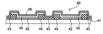
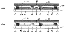
우선 도 1에 의해, 본 실시 형태에 있어서의 유기 반도체 소자(40)의 층 구성에 대하여 설명한다. 여기에서는 유기 반도체 소자(40)의 일례로서, 톱 에미션 타입의 유기 EL 소자에 대하여 설명한다.First, the layer structure of the
유기 반도체 소자Organic semiconductor device
도 1에 도시한 바와 같이 유기 반도체 소자(40)는, 기재(41)와, 기재(41) 위에 설치된 복수의 제1 전극(42)과, 제1 전극(42) 사이에 설치된 보조 전극(43) 및 돌기부(44)와, 제1 전극(42) 위에 설치된 유기 반도체층(45)과, 유기 반도체층(45) 위 및 보조 전극(43) 위에 설치된 제2 전극(46)을 구비하고 있다.1, the
유기 반도체층(45)은, 유기 화합물 중에 있어서의 전자와 정공의 재결합에 의해 발광하는 발광층을 적어도 포함하고 있다. 또한 유기 반도체층(45)은, 정공 주입층, 정공 수송층, 전자 수송층 또는 전자 주입층 등, 유기 EL 소자에 있어서 일반적으로 설치되는 다양한 층을 더 포함하고 있어도 된다. 유기 반도체층의 구성 요소로서는 공지된 것을 사용할 수 있지만, 예를 들어 일본 특허공개 제2011-9498호 공보에 기재된 것을 사용할 수 있다.The
제1 전극(42)은, 유기 반도체층(45)의 각각에 대응하여 설치되어 있다. 제1 전극(42)은, 유기 반도체층(45)에서 발생한 광을 반사시키는 반사 전극으로서도 기능하는 것이다. 제1 전극(42)을 구성하는 재료로서는, 알루미늄, 크롬, 티타늄, 철, 코발트, 니켈, 몰리브덴, 구리, 탄탈륨, 텅스텐, 백금, 금, 은 등의 금속 원소의 단체 또는 이들의 합금을 들 수 있다.The
제2 전극(46)은, 복수의 유기 반도체층(45)에 대한 공통 전극으로서 기능하는 것이다. 또한 제2 전극(46)은, 유기 반도체층(45)에서 발생한 광을 투과시키도록 구성되어 있다. 제2 전극(46)을 구성하는 재료로서는, 광을 투과시킬 수 있을 정도로 얇게 된 금속막이나, ITO 등의 산화물 도전성 재료를 사용할 수 있다.The
보조 전극(43)은, 도시를 생략한 전원으로부터 개개의 유기 반도체층까지의 거리의 차에 기인하여 전압 강하의 변동이 발생하지 않도록 하고, 이에 의해, 유기 EL 소자를 사용한 표시 장치의 휘도 변동을 억제하기 위한 것이다. 도 1에 도시한 바와 같이, 각 보조 전극(43)은 제2 전극(46)에 접속되어 있다. 보조 전극(43)을 구성하는 재료로서는, 제1 전극(42)과 마찬가지의 금속 원소의 단체 또는 합금을 들 수 있다. 보조 전극(43)은, 제1 전극(42)과 동일한 재료로 구성되어 있어도 되며, 또는, 제1 전극(42)과는 상이한 재료로 구성되어 있어도 된다.The
돌기부(44)는, 절연성을 갖는 재료로 구성되는 것이다. 도 1에 도시한 예에 있어서, 돌기부(44)는, 제1 전극(42)과 보조 전극(43)의 사이에 설치되어 있다. 이와 같은 돌기부(44)를 설치함으로써, 제1 전극(42)과 보조 전극(43) 및 제2 전극(46) 사이의 절연성을 확보할 수 있다. 또한, 돌기부(44)의 사이에 설치되는 유기 반도체층(45)의 형상을 적절하게 정할 수 있다. 돌기부(44)를 구성하는 재료로서는, 폴리이미드 등의 유기 재료나, 산화실리콘 등의 무기 절연성 재료를 사용할 수 있다. 또한 돌기부(44)는, 기재(41)의 법선 방향을 따라서 연장하도록 구성되어 있으며, 이 때문에 후술하는 덮개재를 기재(41)에 밀착시킬 때, 덮개재와 기재(41)의 사이에 공간을 확보하기 위한 스페이서로서 기능할 수도 있다.The protruding
도 1에 도시한 바와 같이, 유기 반도체층(45) 및 제2 전극(46)은, 제1 전극(42) 위뿐만 아니라 돌기부(44) 위에도 연속하여 설치되어 있어도 된다. 또한, 유기 반도체층(45) 중 전류가 흘러서 발광하는 것은, 제1 전극(42)과 제2 전극(46)에 의해 상하로 끼어 있는 부분이며, 돌기부(44) 위에 위치하는 유기 반도체층(45)에서는 발광이 발생하지 않는다. 후술하는 도 2a 및 도 2b에 있어서는, 유기 반도체층(45) 중 발광이 발생하는 부분, 즉 제1 전극(42) 위에 설치된 유기 반도체층(45)이 도시되어 있다.The
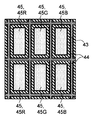
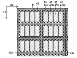
다음으로, 기재(41)의 법선 방향으로부터 본 경우의 유기 반도체 소자(40)의 구조에 대하여 설명한다. 특히, 유기 반도체 소자(40)의 보조 전극(43), 돌기부(44) 및 유기 반도체층(45)의 레이아웃에 대하여 설명한다. 도 2a는, 보조 전극(43), 돌기부(44) 및 유기 반도체층(45)의 레이아웃의 일례를 나타내는 평면도이다. 도 2a에 도시한 바와 같이, 유기 반도체층(45)은, 매트릭스 형상으로 순서대로 배치되고, 각각이 직사각형 형상을 갖는 적색 유기 반도체층(45R), 녹색 유기 반도체층(45G) 및 청색 유기 반도체층(45B)을 포함하고 있어도 된다. 이 경우, 적색 유기 반도체층(45R), 녹색 유기 반도체층(45G) 및 청색 유기 반도체층(45B)의 각각이, 서브 화소를 구성하고 있다. 또한, 인접하는 유기 반도체층(45R, 45G, 45B)의 조합이 하나의 화소를 구성하고 있다.Next, the structure of the
도 2a에 도시한 바와 같이, 보조 전극(43)은, 매트릭스 형상으로 배치된 유기 반도체층(45)의 사이를 연장하도록 격자 형상으로 배치되어 있다. 이와 같이 보조 전극(43)을 배치함으로써, 각 유기 반도체층(45)에 접속된 제2 전극(46)에 있어서의 전압 강하에, 장소에 따른 차가 발생하는 것을 억제할 수 있다. 또한 도 2a에 도시한 바와 같이, 돌기부(44)는, 제1 전극(42) 위에 설치된 유기 반도체층(45)을 측방으로부터 둘러싸도록, 유기 반도체층(45)과 보조 전극(43)의 사이에 설치되어 있다. 즉, 돌기부(44)는, 제1 전극(42) 위에 설치된 유기 반도체층(45)의 4변을 따라 연속해서 설치되어 있다. 이에 의해, 보조 전극(43) 위의 유기 반도체층(45)을 제거하는 공정에 있어서, 비산된 유기 반도체 재료가 제1 전극(42) 위의 유기 반도체층(45)에 도달되는 것을 방지할 수 있다.As shown in Fig. 2A, the
또한 전압 강하를 적절하게 저감할 수 있는 한, 보조 전극(43)이 그 전역에 걸쳐 제2 전극(46)에 접속될 필요는 없다. 즉, 후술하는 제거 공정에 있어서, 보조 전극(43) 위의 유기 반도체층(45)의 모두가 제거될 필요는 없다. 따라서 도 2b에 도시한 바와 같이, 돌기부(44)는, 유기 반도체층(45)의 4변 중 임의의 변을 따라서 비연속적으로 설치되어 있어도 된다. 도 2b에 도시한 예에 있어서도, 돌기부(44)에 의해 끼인 위치에 있는 보조 전극(43) 위의 유기 반도체층(45)을 제거하는 공정에 있어서, 비산된 유기 반도체 재료가, 적어도 부분적으로 돌기부(44)에 의해 끼인 영역 내에 위치하는 제1 전극(42) 위의 유기 반도체층(45)에 도달되는 것을 방지할 수 있다. 또한, 돌기부(44)에 의해 끼인 위치에 있는 보조 전극(43)을 제2 전극(46)에 접속함으로써, 전압 강하를 적절하게 억제할 수 있다.As long as the voltage drop can be appropriately reduced, the
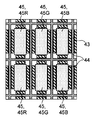
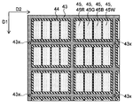
또한, 제2 전극(46)의 전압 강하를 적절하게 억제할 수 있는 한, 보조 전극(43)의 배치가 특별히 한정되지는 않는다. 예를 들어 도 2c나 도 2d에 도시한 바와 같이, 보조 전극(43)은, 복수의 서브 화소에 대응하는 유기 반도체층(45R, 45G, 45B, 45W)에 의해 구성되는 각 화소를 따르도록 설치되어 있어도 된다. 즉, 서브 화소인 유기 반도체층(45R, 45G, 45B, 45W)의 사이에는 보조 전극(43)이 형성되지 않고, 유기 반도체층(45R, 45G, 45B, 45W)에 의해 구성된 하나의 화소와, 그 밖의 마찬가지의 화소와의 사이에 보조 전극(43)이 형성되어 있어도 된다. 또한 도 2c 및 도 2d에 있어서는, 각 화소가, 서브 화소로서, 적색 유기 반도체층(45R), 녹색 유기 반도체층(45G) 및 청색 유기 반도체층(45B)에 추가하여, 백색 유기 반도체층(45W)을 더 포함하는 예가 도시되어 있다.The arrangement of the
또한, 제2 전극(46)의 전압 강하를 적절하게 억제할 수 있는 한, 보조 전극(43)과 제2 전극(46)이 접속되는 개소의 배치가 특별히 한정되지는 않는다. 도 2c 및 도 2d에 있어서, 보조 전극(43)과 제2 전극(46)이 접속되는 개소가, 부호(43x)가 부여된 점선에 의해 도시되어 있다. 도 2c에 도시한 바와 같이, 보조 전극(43)과 제2 전극(46)은, 복수의 개소에서 이산적으로 접속되어 있어도 된다. 즉, 보조 전극(43) 위의 유기 반도체층(45)이, 복수의 개소에서 이산적으로 제거되어도 된다. 또한 도 2d에 도시한 바와 같이, 보조 전극(43)과 제2 전극(46)은, 보조 전극(43)이 연장되는 방향을 따라서 선 형상으로 접속되어 있어도 된다. 즉, 보조 전극(43) 위의 유기 반도체층(45)이, 보조 전극(43)이 연장되는 방향을 따라서 선 형상으로 제거되어도 된다. 도 2d에 있어서는, 일례로서, 보조 전극(43) 위의 유기 반도체층(45)이, 후술하는 덮개재(21)가 반송되는 방향 D1을 따라 선 형상으로 제거되는 예가 도시되어 있다.The arrangement of the portions where the
또한 도 2a 내지 도 2d에 있어서는, 유기 반도체층(45)으로서, 복수의 종류의 유기 반도체층(45R, 45G, 45B, 45W)이 사용되는 예를 나타내었지만, 이에 한정되지는 않는다. 예를 들어, 서브 화소를 구성하는 유기 반도체층(45)은 모두, 공통의 백색광을 생성하도록 구성되어 있어도 된다. 이 경우, 각 서브 화소의 색 분리를 행하는 수단으로서는, 예를 들어 컬러 필터 등이 사용될 수 있다.2A to 2D, an example in which a plurality of kinds of organic semiconductor layers 45R, 45G, 45B, and 45W are used as the
다음으로, 본 실시 형태에 의한 유기 반도체 소자(40)를 기재(41) 위에 형성하기 위한 소자 제조 장치(10) 및 소자 제조 방법에 대하여 설명한다. 유기 반도체 소자(40)에 불순물이 혼입되는 것을 충분히 방지할 수 있는 한, 소자 제조 방법이 실시되는 환경은 특별히 한정되지는 않지만, 예를 들어 소자 제조 방법은 부분적으로 진공 환경하에서 실시된다. 또한 적어도 대기압보다도 저압의 환경인 범위에 있어서, 진공 환경에 있어서의 구체적인 압력이 특별히 한정되지는 않지만, 예를 들어 소자 제조 장치(10)의 내부 압력은 1.0×10⁴Pa 이하로 되어 있다.Next, an
소자 제조 장치Device manufacturing apparatus
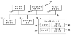
도 3은, 소자 제조 장치(10)를 개략적으로 나타내는 도면이다. 도 3에 도시한 바와 같이, 소자 제조 장치(10)는, 기재(41) 위에 복수의 제1 전극(42)을 형성하는 제1 전극 형성 장치(11)와, 제1 전극(42) 사이에 보조 전극(43)을 형성하는 보조 전극 형성 장치(12)와, 제1 전극(42)과 보조 전극(43)의 사이에 돌기부(44)를 형성하는 돌기부 형성 장치(13)와, 제1 전극(42), 보조 전극(43) 위 및 돌기부(44) 위에 유기 반도체층(45)을 형성하는 유기 반도체층 형성 장치(14)를 구비하고 있다. 이하의 설명에 있어서, 각 장치(11, 12, 13, 14)를 사용한 공정에 의해 얻어지는 것을 중간 제품(50)이라 칭하는 경우도 있다.Fig. 3 is a view schematically showing the
소자 제조 장치(10)는, 후술하는 덮개재가 중간 제품(50)의 일부에 대하여 밀착되어 있는 동안에 소정의 처리를 실시하는 중간 제품 처리 장치(15)를 더 구비하고 있다. 본 실시 형태에 있어서는, 중간 제품 처리 장치(15)가, 보조 전극(43) 위에 설치된 유기 반도체층(45)을 제거하는 제거 장치로서 구성되어 있는 예에 대하여 설명한다. 중간 제품 처리 장치(15)는, 스테이지(18), 덮개재 공급 기구(20), 밀봉 기구(30) 및 조사 기구(25)를 갖고 있다. 중간 제품 처리 장치(15)의 각 구성 요소에 대해서는 후술한다. 덮개재(21) 또한 소자 제조 장치(10)는, 보조 전극(43) 위의 유기 반도체층(45)가 제거된 후에 보조 전극(43) 및 유기 반도체층(45) 위에 제2 전극(46)을 형성하는 제2 전극형 장치(16)를 더 구비하고 있다.The
각 장치(11 내지 16)에 의해 실시되는 공정은 모두 진공 환경하에서 행해진다. 도 3에 도시한 바와 같이, 소자 제조 장치(10)는, 진공 환경을 유지하면서 각 장치(11 내지 16) 사이에서 기재(41)나 중간 제품(50)을 반송하기 위해 각 장치(11 내지 16)에 접속된 반송 장치(17)를 더 구비하고 있어도 된다.The processes performed by the
또한 도 3은, 기능적인 관점으로부터 각 장치를 분류한 것이며, 물리적인 형태가 도 3에 도시한 예로 한정되지는 않는다. 예를 들어, 도 3에 도시한 각 장치(11 내지 16) 중 복수의 장치가, 물리적으로는 하나의 장치에 의해 구성되어 있어도 된다. 또는, 도 3에 도시한 각 장치(11 내지 16) 중 어느 하나는, 물리적으로는 복수의 장치에 의해 구성되어 있어도 된다. 예를 들어 후술하는 바와 같이, 제1 전극(42) 및 보조 전극(43)은 하나의 공정에 있어서 동시에 형성되는 경우가 있다. 이 경우, 제1 전극 형성 장치(11) 및 보조 전극 형성 장치(12)는 하나의 장치로서 구성되어 있어도 된다.Further, Fig. 3 shows each device classified from the viewpoint of function, and the physical form is not limited to the example shown in Fig. For example, a plurality of devices among the
소자 제조 방법Device manufacturing method
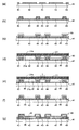
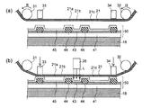
이하, 도 4의 (a) 내지 (g)를 참조하여, 소자 제조 장치(10)를 사용하여 유기 반도체 소자(40)를 제조하는 방법에 대하여 설명한다. 처음에, 예를 들어 스퍼터링법에 의해, 제1 전극(42) 및 보조 전극(43)을 구성하는 금속 재료의 층을 기재(41) 위에 형성하고, 이어서 금속 재료의 층을 에칭에 의해 성형한다. 이에 의해, 도 4의 (a)에 도시한 바와 같이, 전술한 제1 전극(42) 및 보조 전극(43)을 동시에 기재(41) 위에 형성할 수 있다. 또한, 제1 전극(42)을 형성하는 공정 및 보조 전극(43)을 형성하는 공정은, 별개로 실시되어도 된다.Hereinafter, a method of manufacturing the
다음으로, 도 4의 (b)에 도시한 바와 같이, 예를 들어 포토리소그래피법에 의해, 제1 전극(42)과 보조 전극(43)의 사이에, 제1 전극(42) 및 보조 전극(43)보다도 상방까지 기재(41)의 법선 방향을 따라서 연장되는 복수의 돌기부(44)를 형성한다. 그 후, 증착법, CVD법, 인쇄법, 잉크젯법 또는 전사법 등의 일반적인 성막 방법에 의해, 도 4의 (c)에 도시한 바와 같이, 제1 전극(42) 위, 보조 전극(43) 위 및 돌기부(44) 위에 유기 반도체층(45)을 형성한다. 이와 같이 하여, 기재(41)와, 기재(41)에 설치된 복수의 제1 전극(42)과, 제1 전극(42) 사이에 설치된 보조 전극(43) 및 돌기부(44)와, 제1 전극(42) 위, 보조 전극(43) 위 및 돌기부(44) 위에 설치된 유기 반도체층(45)을 포함하는 중간 제품(50)을 얻을 수 있다. 또한 본 실시 형태에 있어서는, 전술한 바와 같이, 제1 전극(42) 및 보조 전극(43)이 돌기부(44)보다도 먼저 기재(41) 위에 형성된다. 이로 인해, 제1 전극(42) 및 보조 전극(43)은, 돌기부(44)에 의해 부분적으로 덮여 있다.4 (b), a
다음으로, 덮개재(21)를 준비하고, 그 후, 도 4의 (d)에 도시한 바와 같이, 덮개재(21)의 제1 면(21a)을 중간 제품(50)의 일부에 밀착시킨다. 이어서, 덮개재(21)가 중간 제품(50)에 밀착되어 있는 동안에, 도 4의 (e)에 도시한 바와 같이, 보조 전극(43) 위에 설치된 유기 반도체층(45)에 레이저광 등의 광 L을 조사한다. 이에 의해, 광 L의 에너지가 유기 반도체층(45)에 의해 흡수되고, 이 결과, 보조 전극(43) 위의 유기 반도체층(45)을 구성하는 유기 반도체 재료가 비산된다. 이와 같이 하여, 보조 전극(43) 위의 유기 반도체층(45)을 제거할 수 있다. 보조 전극(43) 위로부터 비산된 유기 반도체 재료는, 예를 들어 도 4의 (e)에 도시한 바와 같이, 덮개재(21)의 제1 면(21a)에 부착된다. 도 4의 (f)는 보조 전극(43) 위의 유기 반도체층(45)이 제거된 상태를 나타내는 도면이다.4 (d), the
그 후, 도 4의 (g)에 도시한 바와 같이, 제1 전극(42) 위의 유기 반도체층(45) 위 및 보조 전극(43) 위에 제2 전극(46)을 형성한다. 이와 같이 하여, 제2 전극(46)에 접속된 보조 전극(43)을 구비하는 유기 반도체 소자(40)를 얻을 수 있다.4 (g), a
(중간 제품 처리 장치)(Intermediate product processing equipment)
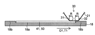
전술한 도 4의 (d), (e)를 참조하여 설명한, 덮개재(21)를 중간 제품(50)의 일부에 밀착시킴과 함께 보조 전극(43) 위의 유기 반도체층(45)을 제거하는 방법에 대하여, 도 5 및 도 6을 참조하여 보다 상세히 설명한다. 또한 도 4의 (d), (e)에 도시한 공정은, 전술한 중간 제품 처리 장치(15)에 의해 실시된다. 처음에 도 5를 참조하여, 중간 제품 처리 장치(15)의 구성에 대하여 상세히 설명한다. 도 5에 있어서는, 서로 직교하는 제1 방향, 제2 방향 및 제3 방향이 각각 화살표 D1, D2 및 D3으로 도시되어 있다.The
도 5에 도시한 바와 같이, 중간 제품 처리 장치(15)는, 중간 제품(50)이 적재되는 스테이지(18)와, 긴 형상의 덮개재(21)를 공급하는 덮개재 공급 기구(20)와, 덮개재(21)의 일부를 중간 제품(50)의 일부에 밀착시키는 밀봉 기구(30)와, 중간 제품(50) 중 덮개재(21)가 밀착하고 있는 부분에 대하여 광을 조사하는 조사 기구(25)를 구비하고 있다. 중간 제품 처리 장치(15)의 각 구성 요소는, 진공 분위기로 유지된 챔버 속에 배치되어 있다. 이로 인해, 보조 전극(43) 위의 유기 반도체층(45)을 제거하는 공정을, 진공 환경하에서 실시할 수 있다. 이하, 중간 제품 처리 장치(15)의 각 구성 요소에 대하여 설명한다. 또한 「긴 형상」이란, 덮개재(21)가 반송되는 방향에 있어서의 덮개재(21)의 치수가, 덮개재(21)가 반송되는 방향으로 직교하는 방향에 있어서의 덮개재(21)의 치수의 적어도 5배 이상으로 되어 있음을 의미하고 있다.5, the intermediate
(스테이지)(stage)
스테이지(18)는, 중간 제품(50)을 지지하기 위한 적재면(18a)을 갖고 있으며, 이 적재면(18a)은, 제1 방향 D1 및 제2 방향 D2에 평행으로 펼쳐져 있다. 또한 스테이지(18)는, 제1 방향 D1에 평행한 스테이지 이동 방향 T1에 있어서 이동 가능하도록 구성되어 있다. 또한 중간 제품(50)은, 전술한 복수의 돌기부(44)가 제1 방향 D1을 따라 기재(41) 위에 배열되도록, 스테이지(18)에 적재되어 있다. 이로 인해, 후술하는 바와 같이, 스테이지(18)를 스테이지 이동 방향 T1을 따라 이동시키는 것과, 조사 기구(25)에 의해 중간 제품(50)을 향해 광을 조사하는 것을 반복함으로써, 중간 제품(50) 중 제1 방향 D1을 따라 배열되는 복수의 돌기부(44) 또는 그 주변 부분에 대하여 순차 광을 조사하는 것이 가능해진다. 또한 스테이지(18)에 적재되어 있는 중간 제품(50)의 돌기부(44)는, 제1 방향 D1 및 제2 방향 D2에 직교하는 제3 방향 D3을 따라 연장되어 있다.The
(덮개재 공급 기구 및 밀봉 기구(30))(The cover re-supply mechanism and the sealing mechanism 30)
도 5에 도시한 바와 같이, 밀봉 기구(30)는, 제1 방향 D1에 직교하는 제2 방향 D2로 연장되는 회전축을 중심으로 하여 회전 방향 R에 있어서 회전하는 한 쌍의 롤러(31, 32)를 갖고 있다. 한 쌍의 롤러(31, 32)는, 제1 롤러(31) 및 제2 롤러(32)로 이루어져 있다. 한편, 덮개재 공급 기구(20)는, 도시를 생략하였지만, 제1 롤러(31)와 중간 제품(50)의 사이를 향해 조출 방향 T2를 따라 덮개재(21)를 풀어내는 조출부와, 제2 롤러(32)와 중간 제품(50)의 사이를 통과한 후의 덮개재(21)를 권취 방향 T3을 따라 권취하는 권취부를 갖고 있다. 이와 같이 본 실시 형태에 있어서는, 중간 제품(50)의 일부를 덮기 위한 덮개재(21)가, 롤·투·롤에의해 공급된다. 이하의 설명에 있어서, 덮개재(21)의 면 중 스테이지(18)측을 향하는 면을 제1 면(21a)이라 칭하고, 제1 면(21a)의 반대측에 있는 면을 제2 면(21b)이라 칭한다. 각 롤러(31, 32)는 각각 덮개재(21)의 제2 면(21b)에 접촉한다.5, the
덮개재(21)를 구성하는 재료로서는, 레이저광 등의 광을 투과시킬 수 있도록, PET(폴리에틸렌테레프탈레이트), COP(시클로올레핀 중합체), PP(폴리프로필렌), PE(폴리에틸렌), PC(폴리카르보네이트), 유리 필름 등의 투광성을 갖는 재료가 사용된다.As the material of the
밀봉 기구(30)의 각 롤러(31, 32)는, 스테이지(18)의 이동에 동기하여 회전하도록 구성되어 있다. 즉 각 롤러(31, 32)는, 스테이지(18)의 이동 속도와 덮개재(21)의 반송 속도가 일치하도록, 각 롤러(31, 32)에 감긴 덮개재(21)를 반송한다. 또한 각 롤러(31, 32)는, 덮개재(21)를 반송할뿐만 아니라, 제1 롤러(31)와 제2 롤러(32)의 사이에 위치하는 덮개재(21)에 소정의 장력을 가할 수 있도록, 구성되어 있다. 이로 인해 덮개재(21) 중 제1 롤러(31)와 제2 롤러(32)의 사이에 위치하는 부분은, 한 쌍의 롤러(31, 32)에 걸쳐진 상태에 있다고 할 수 있다. 이하의 설명에 있어서, 덮개재(21) 중 한 쌍의 롤러(31, 32)에 걸쳐져 있는 부분을, 걸침 부분(21c)이라고도 칭한다. 또한 도시를 생략하였지만, 한 쌍의 롤러(31, 32)에는 각각, 각 롤러(31, 32)를 소정 위치에서 지지하여 회전시키기 위한 구동부가 설치되어 있다.The
중간 제품(50)을 향해 광을 조사하기 위한 경로를 방해하지 않는 한, 각 롤러(31, 32)를 회전시키기 위한 구동부의 구체적인 구성이 특별히 한정되지는 않는다.The specific configuration of the driving unit for rotating the
(조사 기구)(Investigation organization)
도 5에 도시한 바와 같이, 조사 기구(25)는, 레이저광 등의 광 L을 방사하는 광 헤드(26)를 갖고 있다. 광 헤드(26)로부터 방사된 광은, 덮개재(21)의 걸침 부분(21c)을 투과해서 중간 제품(50)에 도달된다. 또한 조사 기구(25)는, 광 L의 초점을 유기 반도체층(45)에 대하여 맞추기 위한 렌즈 등을 더 포함하고 있어도 된다.As shown in Fig. 5, the
광 헤드(26)는, 스테이지(18)의 이동 및 롤러(31)의 회전에 대하여 고정되어 있다. 즉, 스테이지(18) 및 롤러(31)로부터 독립적으로 배치되어 있다. 예를 들어, 광 헤드(26)는, 스테이지(18)가 이동하거나, 롤러(31)가 회전하거나 해도, 광 헤드(26)에 의해 생성되는 광 L의 진행 방향이 변화되지 않도록, 구성되어 있다. 한편, 전술한 바와 같이, 스테이지(18)는 제1 방향 D1로 이동 가능하며, 또한 중간 제품(50)의 돌기부(44)는 제1 방향 D1을 따라 배열되어 있다. 따라서, 광 헤드(26)가 정지 상태에 있는 경우라도, 복수의 돌기부(44) 또는 그 주변 부분에 대하여 순차 광을 조사하는 것이 가능하게 되어 있다. 또한 광 헤드(26)를 제1 방향 D1에 있어서 이동시킬 필요가 없으므로, 공정이 행해지는 동안 광 헤드(26)의 조준이 어긋나는 경우가 없다. 따라서, 광 헤드(26)를 이동시키면서 중간 제품(50)의 복수의 부분에 광을 조사하는 경우에 비하여, 높은 위치 정밀도로 광을 조사할 수 있다.The
광 헤드(26)는, 도 5에 있어서 화살표 M으로 도시되어 있는 바와 같이, 제2 방향 D2, 즉 각 롤러(31, 32)의 회전축을 따른 방향에 있어서 이동 가능하도록 구성되어 있어도 된다. 이에 의해, 후술하는 바와 같이, 중간 제품(50)의 임의의 부분에 광을 조사하는 것이 가능해진다. 광 헤드(26)를 이동시키기 위한 구체적인 구성은 특별히 한정되지는 않는다. 예를 들어 광 헤드(26)는, 스테이지(18)의 상방에 배치된 레일(27)을 따라 이동할 수 있다. 또한, 광 헤드(26)가 정지 상태에 있는 경우라도, 광 헤드(26)가, 제2 방향의 임의의 위치에서 광을 선택적으로 취출하는 것이 가능하게 구성되어 있는 경우에는, 제2 방향의 임의의 위치에서 중간 제품(50)을 향해 광을 조사하는 것이 가능해진다. 제2 방향의 임의의 위치에서 광을 선택적으로 취출하는 방법으로서는, 예를 들어, 도시를 생략하였지만, 복수의 개구부가 형성된 마스크를 조사 기구(25)와 덮개재(21)의 사이에 배치하고, 또한 마스크의 개구부를 선택적으로 차폐하는 방법이 고려된다.The
제2 방향의 임의의 위치에서 중간 제품(50)을 향해 광을 조사하는 것이 가능한 경우, 중간 제품(50) 중 광이 조사되어야 할 부분은, 제2 방향에 직교하는 제1 방향을 따라서 배열되지 않아도 된다. 따라서, 도시를 생략하였지만, 중간 제품(50)의 돌기부(44)는, 제1 방향 D1을 따라 배열되지 않아도 된다.When it is possible to irradiate light toward the
다음으로 도 6을 참조하여, 중간 제품 처리 장치(15)를 사용하여 보조 전극(43) 위의 유기 반도체층(45)을 제거하는 방법을 설명한다.Next, a method of removing the
처음에, 제1 면(21a)을 갖는 덮개재(21)를, 제1 면(21a)이 중간 제품(50)의 돌기부(44)측을 향하도록 준비한다. 예를 들어, 덮개재 공급 기구(20)를 사용하여, 덮개재(21)의 제1 면(21a)이 스테이지(18)측을 향하도록 덮개재(21)를 제1 롤러(31)와 중간 제품(50)의 사이에 공급하는 덮개재 공급 공정을 실시한다. 이어서, 밀봉 기구(30)의 한 쌍 롤러(31, 32)를 사용하여, 덮개재(21)의 제1 면(21a)의 일부를 중간 제품(50)에 가압하는 밀봉 공정을 실시한다. 이에 의해, 덮개재(21)의 제1 면(21a)의 일부가 중간 제품(50)의 일부에 밀착된다. 구체적으로는, 도 6에 도시한 바와 같이, 덮개재(21)의 걸침 부분(21c)의 제1 면(21a)이, 중간 제품(50)의 일부에 밀착된다. 여기서 전술한 바와 같이, 한 쌍의 롤러(31, 32)에 걸쳐져 있는 덮개재(21)의 걸침 부분(21c)에는, 소정의 장력이 가해져 있다. 또한 덮개재(21) 중 한 쌍의 롤러(31, 32)에 접촉하고 있는 부분은 각각, 도 6에 도시한 바와 같이, 중간 제품(50)을 향해 가압되어 있다. 이로 인해, 덮개재(21) 중 한 쌍의 롤러(31, 32)에 접촉하고 있는 부분뿐만 아니라, 한 쌍의 롤러(31, 32) 사이에 있는 걸침 부분(21c)도, 중간 제품(50)에 대하여 소정의 압력으로 가압된 상태에 있다. 예를 들어 도 6에 도시한 예에 있어서, 걸침 부분(21c)은, 중간 제품(50) 중 돌기부(44)가 설치되어 있는 부분에 대하여 소정의 압력으로 가압되어 있다. 따라서, 덮개재(21)의 제1 면(21a)을, 중간 제품(50) 중 돌기부(44)가 설치되어 있는 부분에 간극 없이 밀착시킬 수 있다.Firstly, the
그 후, 중간 제품(50) 중 덮개재(21)에 밀착되어 있는 부분에 대하여 덮개재(21)를 개재하여 광을 조사하는 조사 공정을 실시한다. 또한 「덮개재(21)에 밀착되어 있는 부분」이란, 덮개재(21)의 제1 면(21a)에 직접적으로 접하고 있는 돌기부(44)의 부분뿐만 아니라, 덮개재(21)의 제1 면(21a)에 밀착되어 있는 돌기부(44)의 부분에 의해 둘러싸여 있는 부분도 포함하는 개념이다. 또한, 중간 제품(50) 중 덮개재(21)에 밀착되어 있는 부분의 모두에 대하여 광을 조사할 필요는 없다. 본 실시 형태에 있어서는, 중간 제품(50) 중, 덮개재(21)에 밀착되어 있는 부분이며, 또한 제거되어야 할 유기 반도체층(45)이 설치되어 있는 부분에 대하여, 광이 조사된다. 도 6에 있어서는, 조사 기구(25)의 광 헤드(26)로부터 방사된 광 L이, 덮개재(21)의 걸침 부분(21c)을 투과해서 중간 제품(50)의 보조 전극(43) 위에 설치된 유기 반도체층(45)에 도달되는 모습이 도시되어 있다. 유기 반도체층(45)이 광 L의 에너지를 흡수함으로써, 전술한 바와 같이, 보조 전극(43) 위의 유기 반도체층(45)을 구성하는 유기 반도체 재료가 비산된다.Thereafter, an irradiation step of irradiating light to the portion of the
여기서 본 실시 형태에 의하면, 전술한 바와 같이, 소정의 장력으로 팽팽하게 늘어진 상태에 있는 걸침 부분(21c)을 덮개재(21)에 형성하고, 이 걸침 부분(21c)을 소정의 압력으로 중간 제품(50)의 일부에 가압하고 있다. 이로 인해, 중간 제품(50) 중 돌기부(44)가 설치되어 있는 부분에, 덮개재(21)의 걸침 부분(21c)의 제1 면(21a)을 간극 없이 밀착시킬 수 있다. 이것에 의해, 보조 전극(43) 위로부터 비산된 유기 반도체 재료가 제1 전극(42) 위의 유기 반도체층(45)이나 주위 환경을 오염하는 것을 보다 확실히 방지할 수 있다.According to the present embodiment, as described above, the
이와 같이 본 실시 형태에 의하면, 한 쌍의 롤러(31, 32)라는 간이한 구성 요소를 사용하여, 중간 제품(50)의 일부를 덮개재(21)에 의해 효율적으로 덮을 수 있다. 이로 인해, 높은 품질을 갖는 유기 반도체 소자(40)를 낮은 비용으로 제조할 수 있다.As described above, according to the present embodiment, a part of the
보조 전극(43) 위의 유기 반도체층(45)이 제거되면, 조사 기구(25)로부터의 광은 정지된다. 즉, 중간 제품(50)에 대한 광의 조사가 정지된다.When the
다음으로, 스테이지(18)를 스테이지 이동 방향 T1을 따라 이동시키고, 또한 덮개재(21)를, 각 롤러(31, 32)의 회전 방향 R을 따라 이동시킨다. 그 후, 광 헤드(26)로부터 중간 제품(50)을 향하는 광 L의 경로 위에, 다음에 제거할 보조 전극(43) 위의 유기 반도체층(45)이 도달하면, 조사 기구(25)가 다시 광을 방사한다. 이에 의해, 조사 기구(25)로부터의 광 L이 다시 보조 전극(43) 위의 유기 반도체층(45)에 조사되고, 이러한 점에 의해, 유기 반도체층(45)이 제거된다. 이와 같이 하여, 스테이지 이동 방향 T1에 평행한 제1 방향 D1을 따라 배열되는 복수의 보조 전극(43) 위의 유기 반도체층(45)을 순차 제거할 수 있다. 또한 통상은, 보조 전극(43) 위의 유기 반도체층(45)은 기재(41) 위에서 등간격으로 배열되어 있다. 따라서, 보조 전극(43) 사이의 간격과 스테이지(18)의 이동 속도를 고려한 일정한 주기로 조사 기구(25)로부터의 광의 방사를 온 오프시키고, 이에 의해 보조 전극(43) 위의 유기 반도체층(45)에 순차 광을 조사해도 된다.The
이와 같이 스테이지(18)가 이동하고, 또한 한 쌍의 롤러(31, 32)가 회전할 때, 전술한 바와 같이, 조사 기구(25)의 광 헤드(26)는 정지된 상태 그대로 되어 있다. 이로 인해 본 실시 형태에 의하면, 높은 위치 정밀도로 중간 제품(50)에 광을 조사할 수 있고, 이러한 점에 의해, 보조 전극(43)의 유기 반도체층(45)을 정확하게 제거할 수 있다.When the
또한 본 실시 형태에 의하면, 롤·투·롤에 의해 공급되는 덮개재(21)를 사용하여, 이동하는 스테이지(18) 위의 중간 제품(50)을 덮을 수 있다. 이로 인해, 보조 전극(43) 위의 유기 반도체층(45)을 제거하는 전술한 공정을, 덮개재(21)가 감긴 하나의 롤체를 사용하여, 복수의 중간 제품(50)에 대하여 실시할 수 있다. 따라서, 하나의 중간 제품(50)마다 덮개재(21)를 절단하기 위한 장치나 공정은 불필요하며, 이로 인해, 장치 구성이나 공정을 간이한 것으로 할 수 있다. 또한, 덮개재(21)의 절단에 기인하는 찌꺼기가 발생하고, 이에 의해 중간 제품(50)이 오염되어 버리는 것을 방지할 수 있다.Further, according to the present embodiment, the
그 후, 전술한 공정에 의해 제거된 유기 반도체층(45)이 존재하고 있던 제1 방향 D1의 라인과는 상이한 라인 위에 위치하는 복수의 보조 전극(43) 위의 유기 반도체층(45)을 제거하기 위해서, 레일(27)을 따라 광 헤드(26)를 이동시켜도 된다. 광 헤드(26)를 이동시킨 후, 스테이지(18)를 이동시키면서 전술한 공정을 다시 실시함으로써, 새로운 라인 위에 위치하는 복수의 보조 전극(43) 위의 유기 반도체층(45)을 제거할 수 있다.Thereafter, the
또한, 전술한 실시 형태에 대해 다양한 변경을 가하는 것이 가능하다. 이하, 도면을 참조하면서, 변형예에 대하여 설명한다. 이하의 설명 및 이하의 설명에서 이용하는 도면에서는, 전술한 실시 형태와 마찬가지로 구성될 수 있는 부분에 대하여, 전술한 실시 형태에 있어서의 대응하는 부분에 대해 사용한 부호와 동일한 부호를 사용하도록 하고, 중복되는 설명을 생략한다. 또한, 전술한 실시 형태에 있어서 얻어지는 작용 효과가 변형예에 있어서도 얻어지는 것이 명백한 경우, 그 설명을 생략하는 경우도 있다.It is also possible to make various modifications to the above-described embodiment. Hereinafter, modifications will be described with reference to the drawings. In the drawings used in the following description and the following description, the same reference numerals as those used for the corresponding parts in the above-described embodiments are used for the parts that can be configured similarly to the above-described embodiments, The description will be omitted. In addition, in the case where it is apparent that the action and effect obtained in the above-described embodiment is also obtained in the modified example, the description thereof may be omitted.
(유기 반도체 소자의 층 구성의 변형예)(Modification of Layer Configuration of Organic Semiconductor Device)
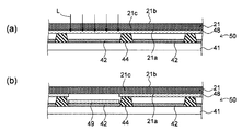
전술한 본 실시 형태에 있어서, 제1 전극(42) 및 보조 전극(43)이 돌기부(44)보다도 먼저 기재(41) 위에 형성되는 예를 나타내었다. 그러나, 이에 한정되지 않고, 돌기부(44)를 제1 전극(42) 및 보조 전극(43)보다도 먼저 기재(41) 위에 형성하여도 된다. 이러한 경우에도, 전술한 본 실시 형태에 의한 밀착 공정이나 제거 공정을 이용할 수 있다. 이하, 이와 같은 예에 대하여 도 7의 (a) 내지 (g)를 참조하여 설명한다.An example in which the
처음에 도 7의 (a)에 도시한 바와 같이, 기재(41) 위에 복수의 돌기부(44)를 형성한다. 이어서, 도 7의 (b)에 도시한 바와 같이, 돌기부(44) 사이에 제1 전극(42)을 형성함과 함께, 돌기부(44) 위에 보조 전극(43)을 형성한다. 이에 의해, 돌기부(44)에 의해 서로 절연된 복수의 제1 전극(42)과, 돌기부(44) 위에 설치된 보조 전극(43)을 얻을 수 있다. 또한 도시를 생략하였지만, 처음에 기재(41) 위에 제1 전극(42)을 형성하고, 이어서 제1 전극(42)의 사이에 돌기부(44)를 형성하고, 그 후, 돌기부(44) 위에 보조 전극(43)을 형성하여도 된다.First, as shown in FIG. 7 (a), a plurality of protruding
그 후, 도 7의 (c)에 도시한 바와 같이, 제1 전극(42), 보조 전극(43) 및 돌기부(44) 위에 유기 반도체층(45)을 형성한다. 이와 같이 하여, 기재(41)와, 기재(41)에 설치된 복수의 제1 전극(42)과, 제1 전극(42) 사이에 설치된 보조 전극(43) 및 돌기부(44)와, 제1 전극(42) 위 및 보조 전극(43) 위에 설치된 유기 반도체층(45)을 포함하는 중간 제품(50)을 얻을 수 있다. 또한 본 변형예에 있어서는, 보조 전극(43)보다도 먼저 돌기부(44)가 형성되기 때문에, 돌기부(44)가 보조 전극(43)에 의해 덮여 있다. 또한 돌기부(44)는, 그 상면이 전역에 걸쳐 보조 전극(43)에 의해 덮여 있을 필요는 없다. 즉 돌기부(44)는, 그 상면이 적어도 부분적으로 보조 전극(43)에 의해 덮여 있으면 된다. 또한 전술한 본 실시 형태에 있어서는, 제1 전극(42) 사이에 2열에 걸쳐 돌기부(44)가 설치되고, 돌기부(44) 사이에 보조 전극(43)이 설치되는 예를 나타내었지만, 본 변형예에 있어서는, 보조 전극(43)이 돌기부(44) 위에 설치되기 때문에, 도 7의 (c)에 도시한 바와 같이 제1 전극(42) 사이에 설치되는 돌기부(44)는 1열뿐이어도 된다.7 (c), the
다음으로 도 7의 (d)에 도시한 바와 같이, 밀봉 기구(30)의 한 쌍 롤러(31, 32)를 사용하여, 덮개재(21)의 걸침 부분(21c)을 중간 제품(50)의 일부에 가압하고, 이에 의해, 덮개재(21)의 제1 면(21a)의 일부를 중간 제품(50)의 일부에 밀착시키는 덮개재 밀착 공정을 실시한다. 또한 도 7의 (d) 및 후술하는 도 7의 (e)에 있어서는, 중간 제품(50)이 적재되는 스테이지(18)가 생략되었다.7 (d), by using the pair of
본 변형예에 있어서도, 전술한 본 실시 형태의 경우와 마찬가지로, 덮개재(21) 중 한 쌍의 롤러(31, 32)에 접촉되어 있는 부분은 각각, 중간 제품(50)을 향해 가압되어 있다. 이로 인해, 덮개재(21) 중 한 쌍의 롤러(31, 32)에 접촉하고 있는 부분뿐만 아니라, 한 쌍의 롤러(31, 32) 사이에 있는 걸침 부분(21c)도, 중간 제품(50) 중 돌기부(44)가 설치되어 있는 부분에 대하여 소정의 압력으로 가압된 상태에 있다. 이로 인해, 중간 제품(50) 중 돌기부(44)가 설치되어 있는 부분에, 덮개재(21)의 제1 면(21a)을 간극 없이 밀착시킬 수 있다.In this modified example, similarly to the case of the above-described embodiment, the portions of the
그 후, 돌기부(44) 위의 보조 전극(43) 위의 유기 반도체층(45)에 광 L를 조사하고, 이에 의해 도 7의 (e)에 도시한 바와 같이, 보조 전극(43) 위의 유기 반도체층(45)을 덮개재(21)에 부착시킨다. 도 7의 (f)는, 돌기부(44) 위의 보조 전극(43) 위의 유기 반도체층(45)이 제거된 상태를 나타내는 도면이다. 또한 본 변형예에 있어서는, 제거되어야 할 유기 반도체층(45)에 덮개재(21)가 밀착된다. 이 경우, 덮개재(21)의 제1 면(21a)의 표면 에너지를 적절하게 설정함으로써, 광 L을 조사하지 않고, 돌기부(44) 위의 보조 전극(43) 위의 유기 반도체층(45)을 덮개재(21)의 제1 면(21a)으로 전이시키는 것도 가능하다. 즉, 덮개재(21)의 걸침 부재(21c)를 중간 제품(50)의 일부에 밀착시키는 것이, 보조 전극(43) 위에 설치된 유기 반도체층(45)을 제거하는 것을 실현할 수 있다.Thereafter, the light L is irradiated to the
그 후, 도 7의 (g)에 도시한 바와 같이, 제1 전극(42) 위의 유기 반도체층(45) 위 및 돌기부(44) 위의 보조 전극(43) 위에 제2 전극(46)을 형성한다. 이와 같이 하여, 제2 전극(46)에 접속된 보조 전극(43)을 구비하는 유기 반도체 소자(40)를 얻을 수 있다.7 (g), a
(중간 제품 처리 장치가 노광 장치로서 구성되는 예)(Example in which the intermediate product processing apparatus is configured as an exposure apparatus)
또한 전술한 본 실시 형태 및 변형예에 있어서, 중간 제품 처리 장치(15)가, 보조 전극(43) 위의 유기 반도체층(45)을 제거하는 제거 장치로서 사용되는 예를 나타내었다. 그러나, 중간 제품 처리 장치(15)의 응용예가 특별히 한정되지는 않는다. 예를 들어 중간 제품 처리 장치(15)는, 도시를 생략하였지만, 중간 제품(50)에 덮개재(21)가 밀착되어 있는 동안에 중간 제품(50) 중의 피노광층에 대해 광 L을 노광광으로서 조사하는 노광 공정을 실시하는 노광 장치로서 사용되어도 된다.In addition, in the above-described embodiment and modified examples, an example has been shown in which the intermediate
(중간 제품 처리 장치가 증착 장치로서 구성되는 예)(Example in which the intermediate product processing apparatus is configured as a deposition apparatus)
또는, 중간 제품 처리 장치(15)는, 도 8의 (a), (b)에 도시한 바와 같이, 중간 제품(50)에 덮개재(21)가 밀착되어 있는 동안에 증착용 재료(48)에 광을 조사하여 증착용 재료(48)를 기재(41) 위에 증착시키는 증착 장치로서 사용되어도 된다.8 (a) and 8 (b), the intermediate
본 변형예에 있어서는, 도 8의 (a)에 도시한 바와 같이, 증착용 재료(48)가 덮개재(21)의 제1 면(21a)에 설치되어 있다. 또한 도 8의 (a)에 도시한 바와 같이, 중간 제품(50)은, 기재(41)와, 기재(41) 위에 설치된 복수의 돌기부(44)와, 돌기부(44) 사이에 설치된 제1 전극(42)을 갖고 있다. 이 경우, 중간 제품 처리 장치(15)를 사용하여 적외선 등의 광 L을 증착용 재료(48)에 조사하면, 증착용 재료(48)가 증발한다. 보다 구체적으로는, 도 8의 (a)에 도시한 바와 같이 증착용 재료(48) 중 제1 전극(42)과 대향하는 위치에 존재하는 증착용 재료(48)에 광 L을 조사하면, 증착용 재료(48)가 증발하여 기재(41) 위의 제1 전극(42)에 부착된다. 이 결과, 도 8의 (b)에 도시한 바와 같이, 제1 전극(42) 위에 증착층(49)을 형성할 수 있다. 또한 기재(41)와 덮개재(21)의 사이의 공간은, 돌기부(44)에 의해 적절하게 구획되어 있다. 이로 인해, 기재(41)와 덮개재(21) 사이의 공간에서 증착용 재료(48)가 광역에 걸쳐 비산되어 버리는 것을 방지할 수 있다.In this modification, the
또한 증착용 재료(48)를 가열하여 증발시키는 방법은, 상술한 바로 제한되는 것은 아니다. 예를 들어 덮개재(21)의 제1 면(21a)과 유기 반도체층(45)의 사이에, 적외광을 흡수하는 금속 박막을 형성해 두고, 금속 박막에 광을 조사하여 금속 박막을 가열함으로써, 증착용 재료(48)를 가열하여도 된다. 이 경우, 덮개재(21)의 제1 면(21a)에 설치되어 있는 증착용 재료(48)에 직접적으로는 광이 거의 조사되지 않지만, 금속 박막을 개재하여 간접적으로 증착용 재료(48)를 가열할 수 있으므로, 증착용 재료(48)를 증발시킬 수 있다. 증착용 재료(48)에 직접 광이 조사되는 경우, 및 금속 박막을 개재하여 간접적으로 증착용 재료(48)가 가열되는 경우의 어느 것이든, 덮개재(21) 중 만곡 형상이 형성된 부분을 향해 광이 조사된다고 하는 점에서는 공통이다.The method of heating and evaporating the
또한 금속 박막이 자성 재료로 구성되어 있는 경우, 중간 제품(50)에 대한 덮개재(21)의 밀착 정도를 보다 높게 하기 위해서, 덮개재(21)의 주위에 자장을 발생시키거나, 중간 제품(50) 중 덮개재(21)와는 반대 측에 자성체를 배치하거나 하여, 자력에 의해 덮개재(21)가 중간 제품(50)을 향해 끌어 모아지도록 해도 된다.When the metal thin film is made of a magnetic material, a magnetic field is generated around the
(스테이지의 변형예)(Modification of Stage)
중간 제품(50)이 적재되는 스테이지(18)에는, 도 9에 도시한 바와 같이, 제1 방향 D1에 있어서의 중간 제품(50)의 기재(41)의 단부에 인접하도록 기재(41)의 법선 방향으로 돌출된 돌출 영역(18b)이 형성되어 있어도 된다. 돌출 영역(18b)은, 그 상면의 위치가 중간 제품(50)의 상면 위치와 거의 일치하도록 구성되어 있다. 이 경우, 한 쌍의 롤러(31, 32)는, 한쪽 롤러, 예를 들어 제1 롤러(31)가 덮개재(21)를 개재하여 중간 제품(50) 위에 위치하고, 다른 쪽 롤러, 예를 들어 제2 롤러(32)가 덮개재(21)를 개재하여 스테이지(18)의 돌출 영역(18b) 위에 위치하는 상태에서, 덮개재(21)를 걸칠 수 있게 된다. 이로 인해, 덮개재(21)의 걸침 부분(21c)을, 중간 제품(50)의 기재(41)의 단부 근방에 위치를 부여할 수 있게 된다. 이것에 의해, 중간 제품(50) 중 기재(41)의 단부 근방의 부분에 대하여 덮개재(21)의 걸침 부분(21c)을 밀착시키는 것이 가능해진다. 따라서, 중간 제품(50)의 전역에 대하여 중간 제품 처리 장치(15)를 사용한 처리를 실시할 수 있다.9, the
(덮개재의 변형예)(Modification of Cover Member)
전술한 본 실시 형태 및 각 변형예에 있어서는, 덮개재(21)가, 투광성을 갖는 재료로 이루어지는 단일층으로 구성되어 있는 예를 나타내었다. 그러나, 덮개재(21)가 복수의 층으로 구성되어 있어도 된다. 예를 들어 도 10에 도시한 바와 같이, 덮개재(21)는, 제1 필름(22a) 및 제2 필름(22b)을 포함하고 있어도 된다. 제1 필름(22a)이, 스테이지(18)측을 향하는 덮개재(21)의 제1 면(21a)을 구성하고 있으며, 제2 필름(22b)이, 제1 면(21a)의 반대측에 있는 제2 면(21b)을 구성하고 있다. 또한 도 10은, 전술한 제2 방향 D2, 즉 롤러(31, 32)의 회전축 방향을 따라서 덮개재(21)를 절단한 경우를 나타내는 단면도이다.In the above-described embodiment and modified examples, an example is shown in which the
도 10에 도시한 바와 같이, 제1 필름(22a)과 제2 필름(22b)의 사이에는 밀봉재(22c)가 개재되어 있어도 된다. 도 10에 도시한 예에 있어서는, 제2 방향 D2에 있어서의 각 필름(22a, 22b)의 단부 근방에, 각 필름(22a, 22b)의 길이 방향을 따라 연장되는 밀봉재(22c)가 각각 설치되어 있다. 이와 같은 밀봉재(22c)를 설치함으로써, 제1 필름(22a)과 제2 필름(22b)의 사이에 간격을 설치함과 함께, 제1 필름(22a)과 제2 필름(22b) 사이의 공간(23)을 외부로부터 밀봉하는 것이 가능해진다. 예를 들어, 제1 필름(22a)과 제2 필름(22b) 사이의 공간에 공기나 질소 등의 기체를 봉입하는 것이 가능해진다. 이와 같이 내부의 공간(23)에 기체가 봉입된 덮개재(21)를 사용하는 것의 이점에 대하여, 도 11을 참조하여 이하에 설명한다.As shown in Fig. 10, a sealing
여기에서는, 덮개재(21)의 제1 면(21a)을 중간 제품(50)의 일부에 밀착시키는 밀봉 공정이, 진공 환경하 등, 대기압보다도 낮은 압력을 갖는 감압 환경하에서 실시되는 경우를 생각한다. 이 경우, 제1 필름(22a)과 제2 필름(22b)의 사이에 기체가 봉입되어 있으면, 기체의 압력과 감압 환경하의 압력 사이의 차에 기초하여, 덮개재(21)에 봉입되어 있는 기체가 팽창한다. 이 결과, 제1 필름(22a)과 제2 필름(22b) 사이의 간격이 넓어지려고 한다. 즉, 필름(22a, 22b)이 각각 외측을 향해서 팽창되려고 한다. 한편, 덮개재(21) 중 롤러(31, 32)에 접촉하고 있는 부분에 있어서는, 제1 필름(22a)과 제2 필름(22b) 사이의 간격은, 중간 제품(50)과 롤러(31, 32) 사이의 간격에 기초하여 항상 일정하다. 이 경우, 도 11에 도시한 바와 같이, 덮개재(21) 중 한 쌍의 롤러(31, 32) 사이의 부분, 즉 전술한 걸침 부분(21c)에 있어서는, 기체의 팽창에 기초하여 제1 필름(22a)이, 중간 제품(50) 중 돌기부(44)가 존재하지 않은 공간을 향해 팽창되게 된다. 이것은, 이러한 팽창이 발생되지 않는 경우에 비하여, 중간 제품(50) 중 돌기부(44)가 설치되어 있는 부분에 대하여 제1 필름(22a)이 보다 강하게 밀착되는 것을 의미하고 있다. 이로 인해 본 변형예에 의하면, 제1 필름(22a)에 의해 구성되어 있는 덮개재(21)의 제1 면(21a)을, 중간 제품(50) 중 돌기부(44)가 설치되어 있는 부분에 의해 간극 없이 밀착시킬 수 있게 된다. 이것에 의해, 보조 전극(43) 위로부터 비산된 유기 반도체 재료가 제1 전극(42) 위의 유기 반도체층(45)이나 주위 환경을 오염하는 것을 보다 확실히 방지할 수 있다.Here, a case is considered in which the sealing step of bringing the
또한, 제1 필름(22a)과 제2 필름(22b) 사이의 공간(23)에 기체를 봉입할 수 있는 한, 덮개재(21)의 구체적인 구성이 특별히 한정되지는 않는다. 예를 들어 제1 필름(22a)과 제2 필름(22b)의 사이에는, 다수의 중공 부분이 형성된 중공 수지가 설치되어 있어도 된다. 중공 수지의 중공 부분에는 공기 등의 기체가 존재하고 있으며, 이로 인해, 중공 수지가 설치된 덮개재(21)가 진공 환경 하에 놓이면, 중공 수지의 중공 부분의 기체가 팽창하고, 이 결과, 필름(22a, 22b)이 각각 외측을 향해서 팽창되게 된다. 또한 중공 수지를 설치함으로써, 제1 필름(22a)과 제2 필름(22b) 사이의 간격을 안정적으로 유지할 수 있도록 된다. 중공 수지로서는, 예를 들어 스티렌, 아크릴, 실리카 등으로 이루어지는 중공 입자를 함유한 수지나, 다공질 실리카와 같이 중공 구조를 포함하는 수지 등이 사용될 수 있다.Further, the specific constitution of the
(밀봉 기구의 변형예)(Modification of Sealing Mechanism)
또한 전술한 본 실시 형태 및 변형예에 있어서는, 덮개재(21)를 걸치기 위한 한 쌍 롤러(31, 32)에, 덮개재(21)의 제2 면(21b)이 직접적으로 접하는 예를 나타내었다. 그러나, 덮개재(21) 중 중간 제품(50)을 덮는 부분에 장력을 가할 수 있는 한, 밀봉 기구(30)의 구체적인 구성이 특별히 한정되지는 않는다.In the embodiment and the modification described above, an example in which the
예를 들어 도 12에 도시한 바와 같이, 밀봉 기구(30)는, 한 쌍의 롤러(31, 32)와 덮개재(21)의 사이에 설치된 중간 필름을 갖고 있어도 된다. 도 12에 도시한 예에 있어서는, 도시를 생략한 권출부로부터 권출된 긴 형상의 중간 필름이, 한 쌍의 롤러(31, 32)를 따라 반송된 후, 도시를 생략한 권취부에 의해 권취되어 있다. 한 쌍의 롤러(31, 32)는, 중간 필름(35)을 개재하여 덮개재(21)를 중간 제품(50)을 향해 가압하고 있다. 따라서 본 변형예에 있어서도, 전술한 본 실시 형태의 경우와 마찬가지로, 덮개재(21) 중 한 쌍의 롤러(31, 32) 사이에 있는 걸침 부분(21c)은, 중간 필름(35)을 개재하여 중간 제품(50)에 대하여 소정의 압력에 의해 가압된 상태에 있다. 따라서, 덮개재(21)의 제1 면(21a)을, 중간 제품(50) 중 돌기부(44)가 설치되어 있는 부분에 간극 없이 밀착시킬 수 있다.For example, as shown in Fig. 12, the
또한 본 변형예에 의하면, 덮개재(21)가 받는 가압력이나 장력은, 한 쌍의 롤러(31, 32)로부터 덮개재(21)에 직접적으로 가하는 것이 아니라, 중간 필름(35)을 개재하여 덮개재(21)에 가해진다. 여기서 중간 필름(35)은, 한 쌍의 롤러(31, 32)의 사이에 위치하는 부분에 있어서 광역에 걸쳐 덮개재(21)에 접하고 있다. 이로 인해, 덮개재(21)가 받는 가압력이나 장력에 기인하여 덮개재(21)에 주름 등의 변형이 발생해 버리는 것을 억제할 수 있다. 이것에 의해, 덮개재(21)에 발생하는 주름 등의 변형에 기인하여 덮개재(21)와 돌기부(44)의 사이에 간극이 발생해 버릴 가능성을 저감할 수 있다. 또한 본 변형예에 있어서, 권출부(21s)로부터 권출된 덮개재(21)는, 중간 필름(35)과 중첩된 상태에서 중간 제품(50)을 덮은 후, 중간 필름(35)으로부터 분리되어 권취부(21t)에 의해 권취된다.According to this modification, the pressing force and the tension applied to the
중간 필름(35)을 구성하는 재료, 중간 필름(35)의 두께 및 층 구성 등은, 중간 필름(35)을 개재하여 덮개재(21)에 적절히 가압력이나 장력을 가할 수 있도록 선택된다. 예를 들어, 중간 필름(35)을 구성하는 재료로서, 덮개재(21)를 구성하는 재료보다도 높은 탄성 계수를 갖는 재료가 사용된다. 또한, 중간 필름(35)의 두께를 덮개재(21)의 두께보다도 크게 함으로써, 한 쌍의 롤러(31, 32)의 사이에 중간 제품(50)을 향해 돌출되도록 중간 필름(35)을 만곡시키고, 이에 의해, 중간 제품(50)에 대하여 덮개재(21)를 보다 강하게 가압하도록 해도 된다. 또한, 복수의 필름을 적층함으로써 중간 필름(35)을 구성해도 된다. 예를 들어, 중간 필름(35)은, 한 쌍의 필름과, 한 쌍의 필름 사이에 설치된 간섭층을 포함하고 있어도 된다. 한 쌍의 필름으로서는, 예를 들어 각각이 100㎛ 내지 500㎛의 범위 내의 두께를 갖는 한 쌍의 PET 필름 등을 사용할 수 있다. 또한 간섭층을 구성하는 재료로서는, 투광성을 갖는 겔 형상의 재료를 사용할 수 있다. 예를 들어, 투광성을 갖는 광학 점착재, 소위 OCA를 사용할 수 있다.The material constituting the
또한 본 변형예에 있어서, 덮개재(21)의 제1 면(21a)에는, 중간 제품(50)의 보조 전극(43) 위로부터 비산된 유기 반도체 재료가 부착된다. 따라서, 높은 품질을 갖는 유기 반도체 소자(40)를 제조하기 위해서는, 유기 반도체 재료가 부착된 덮개재(21)는, 유기 반도체 소자(40)의 제조 공정에 있어서 재이용되지 않고 폐기되는 것이 바람직하다. 한편, 중간 필름(35)에 유기 반도체 재료가 부착되는 일은 없다. 또한 도 12에 도시한 바와 같이, 덮개재(21)와 중간 필름은, 분리되어 따로 따로 회수된다. 따라서, 그 후에 실시되는 유기 반도체 소자(40)의 제조 공정에 있어서 중간 필름(35)을 재이용하는 것이 가능하다.In this modification, the organic semiconductor material scattered from above the
(밀봉 기구의 그 밖의 변형예)(Other Modifications of Sealing Mechanism)
또한 전술한 본 실시 형태 및 변형예에 있어서는, 덮개재(21)에 장력을 가하기 위한 한 쌍의 걸침 부재로서, 한 쌍의 롤러(31, 32)가 사용되는 예를 나타내었다. 그러나, 덮개재(21) 중 중간 제품(50)을 덮는 부분에 장력을 가할 수 있는 한, 한 쌍의 걸침 부재의 구체적인 구성이 특별히 한정되지는 않는다.Also, in the above-described embodiment and modified examples, an example in which a pair of
예를 들어 도 13의 (a), (b)에 도시한 바와 같이, 밀봉 기구(30)의 한 쌍의 걸침 부재(33, 34)는, 덮개재(21)를 중간 제품(50)을 향해 가압하도록 중간 제품(50)을 향해서 이동 가능하게 구성된 한 쌍의 부재이더라도 된다. 이 경우, 도 13의 (a)에 도시한 바와 같이, 걸침 부재(33, 34)가 덮개재(21)의 제2 면(21b)에 접촉되지 않은 상태일 때, 한 쌍의 롤러(31, 32)에 의해 덮개재(21)가 반송된다. 다음으로 도 13의 (b)에 도시한 바와 같이, 한 쌍의 롤러(31, 32)를 정지시킨 상태에서, 한 쌍의 걸침 부재(33, 34)를 중간 제품(50)을 향해 이동시키고, 한 쌍의 걸침 부재(33, 34)를 덮개재(21)의 제2 면(21b)에 접촉시킨다. 이에 의해, 한 쌍의 걸침 부재(33, 34)의 사이에 덮개재(21)에 장력이 가해진다. 즉, 덮개재(21) 중 한 쌍의 걸침 부재(33, 34)의 사이에 위치하는 부분이, 한 쌍의 걸침 부재(33, 34)에 의해 걸쳐진 상태가 된다. 그 후, 한 쌍의 걸침 부재(33, 34)를 또한 중간 제품(50)을 향해 이동시키고, 덮개재(21)를 중간 제품(50)의 돌기부(44)에 가압한다. 이에 의해, 덮개재(21) 중 한 쌍의 걸침 부재(33, 34) 사이에 있는 걸침 부분(21c)을, 중간 제품(50)에 대하여 소정의 압력으로 가압할 수 있다.13 (a) and 13 (b), for example, the pair of
(광의 조사 방향의 변형예)(Variation of light irradiation direction)
또한 전술한 본 실시 형태 및 변형예에 있어서는, 보조 전극(43) 위에 설치된 유기 반도체층(45)을 향하여, 덮개재(21)측으로부터 광 L가 조사되는 예를 나타내었다. 그러나, 유기 반도체층(45)을 적절하게 가열하는 것이 가능한 한, 광 L의 조사 방향이 특별히 한정되지는 않는다. 예를 들어 도 14의 (a)에 도시한 바와 같이, 중간 제품(50)의 기재(41)측으로부터, 중간 제품(50)에 밀착되어 있는 덮개재(21)를 향해 광 L을 조사하여도 된다. 여기에서 일반적으로 보조 전극(43)은, 금속 원소의 단체 또는 합금에 의해 구성되어 있다. 따라서, 중간 제품(50)에 밀착되어 있는 덮개재(21)를 향해 조사된 광 L은 주로, 보조 전극(43)에 의해 차폐된다. 이 경우, 광 L로서, 보조 전극(43)에 의해 흡수될 수 있는 파장의 광을 사용함으로써, 보조 전극(43)을 가열하고, 이에 의해 보조 전극(43) 위의 유기 반도체층(45)을 가열할 수 있다. 이 결과, 도 14의 (b)에 도시한 바와 같이, 보조 전극(43) 위의 유기 반도체층(45)을 증발시켜서, 덮개재(21)의 제1 면(21a) 위에 부착시킬 수 있다. 또한, 광 L가 미리 정해져 있는 경우, 보조 전극(43)을 구성하는 재료로서, 광 L을 흡수하는 것이 가능한 재료를 사용하도록 해도 된다.In the above-described embodiment and modified examples, the light L is irradiated from the
(그 밖의 변형예)(Other Modifications)
또한 전술한 본 실시 형태 및 각 변형예에 있어서, 제1 방향 D1에 배열되는 복수의 중간 제품(50)의 부분에 대하여 광 L을 순차 조사할 때, 스테이지(18)는 스테이지 이동 방향 T1에 있어서 이동하고, 한편, 조사 기구(25)의 광 헤드(26)는 정지한 채인 예를 나타냈다. 그러나, 이에 한정되지는 않고, 제1 방향 D1에 배열되는 복수의 중간 제품(50)의 부분에 대하여 광 L을 순차 조사할 때, 스테이지(18)가 정지한 채이며, 광 헤드(26)가 제1 방향 D1을 따라 이동하여도 된다.In the above-described embodiment and modified examples, when the light L is sequentially irradiated onto the portions of the plurality of
또한 전술한 본 실시 형태 및 각 변형예에 있어서, 중간 제품(50)을 지지하는 지지 기구로서 스테이지(18)가 사용되는 예를 나타내었다. 그러나, 덮개재(21)를 중간 제품(50)에 밀착시킬 때 중간 제품(50)을 적절하게 지지할 수 있는 한, 중간 제품(50)을 지지하는 지지 기구의 구체적인 구성이 특별히 한정되지는 않는다. 예를 들어, 중간 제품(50)이 롤·투·롤의 형태에 의해 공급되어 반송되는 경우, 중간 제품(50)을 권출하는 권출부, 중간 제품(50)을 권취하는 권취부, 반송되고 있는 중간 제품(50)에 접촉하는 반송 롤이나 가이드 롤 등이, 중간 제품(50)을 지지하는 지지 기구로서 기능하여도 된다. 중간 제품(50)이 롤·투·롤의 형태에 의해 공급되어 반송되는 경우, 중간 제품(50)의 기재(41)는, 긴 형상으로 연장되는 것이며, 또한 중간 제품(50)의 제1 전극(42), 보조 전극(43), 돌기부(44), 유기 반도체층(45) 및 제2 전극(46) 등은, 긴 형상으로 연장되는 기재(41) 위에 형성되어 있다.Further, in the above-described embodiment and modified examples, an example in which the
또한 전술한 본 실시 형태 및 각 변형예에 있어서, 유기 반도체 소자(40)가 유기 EL인 예를 나타내었다. 그러나, 전술한 소자 제조 장치(10) 및 소자 제조 방법에 의해 제조되는 유기 반도체 소자의 타입이 특별히 한정되지는 않는다. 예를 들어 전술한 소자 제조 장치(10) 및 소자 제조 방법을 이용하여, 유기 트랜지스터 디바이스나 유기 태양 전지 디바이스 등의 다양한 유기 반도체 소자를 제조하는 것이 가능하다. 유기 트랜지스터 디바이스에 있어서, 유기 반도체층 및 그 밖의 구성 요소로서는 공지된 것을 사용할 수 있고, 예를 들어 일본 특허공개 제2009-87996호 공보에 기재된 것을 사용할 수 있다. 마찬가지로, 유기 태양 전지 디바이스에 있어서, 유기 반도체층으로 구성되는 광전 변환층 및 그 밖의 구성 요소로서는 공지된 것을 사용할 수 있고, 예를 들어 일본 특허공개 제2011-151195호 공보에 기재된 것을 사용할 수 있다. 또한, 전술한 소자 제조 장치(10) 및 소자 제조 방법은, 유기 반도체 소자의 제조뿐만 아니라, 무기 반도체 소자의 제조에 적용되어도 된다.In addition, in the above-described embodiment and modified examples, an example in which the
또한 전술한 본 실시 형태 및 각 변형예에 있어서, 중간 제품 처리 장치(15)의 각 구성 요소가, 진공 분위기로 유지된 챔버 내에 배치되는 예를 나타내었다. 즉, 중간 제품 처리 장치(15)를 사용하여 중간 제품(50)에 광을 조사하는 공정이, 진공 환경하에서 실시되는 예를 나타내었다. 그러나, 이에 한정되지는 않고, 중간 제품 처리 장치(15)를 사용하여 중간 제품(50)에 광을 조사하는 공정을, 대기압 환경하 등, 진공 환경 이외의 환경하에서 실시하여도 된다.Furthermore, in the above-described embodiment and modified examples, each component of the intermediate
또한, 전술한 실시 형태에 대한 몇 가지 변형예를 설명해 왔지만, 당연히 복수의 변형예를 적절히 조합하여 적용하는 것도 가능하다.Furthermore, although a few modified examples of the above-described embodiment have been described, it is of course possible to apply a plurality of modified examples suitably in combination.
10: 소자 제조 장치
15: 중간 제품 처리 장치
18: 스테이지
18a: 적재면
18b: 돌출 영역
20: 덮개재 공급 기구
21: 덮개재
25: 조사 기구
26: 광 헤드
27: 레일
30: 밀봉 기구
31: 제1 롤러
32: 제2 롤러
40: 유기 반도체 소자
41: 기재
42: 제1 전극
43: 보조 전극
44: 돌기부
45: 유기 반도체층
46: 제2 전극
50: 중간 제품10: Device manufacturing apparatus
15: Intermediate product processing equipment
18: stage
18a:
18b: protruding area
20: cover re-supply mechanism
21: Cover material
25: Investigation mechanism
26: Optical head
27: Rail
30: Sealing mechanism
31: First roller
32: second roller
40: Organic semiconductor device
41: substrate
42: first electrode
43: auxiliary electrode
44: protrusion
45: organic semiconductor layer
46: Second electrode
50: Intermediate product
Claims (16)
상기 기재와, 상기 기재 위에 설치된 복수의 돌기부를 포함하는 중간 제품을 준비하는 공정과,
제1 면 및 상기 제1 면의 반대측에 있는 제2 면을 갖는 덮개재를, 상기 제1 면이 상기 중간 제품의 상기 돌기부측을 향하도록 준비하는 공정과,
상기 덮개재의 상기 제2 면에 접촉하는 밀봉 기구를 사용하여 상기 덮개재의 상기 제1 면의 일부를 상기 중간 제품의 일부에 가압하여, 상기 중간 제품의 일부를 상기 덮개재의 상기 제1 면에 밀착시키는 밀봉 공정을 구비하고,
상기 밀봉 기구는, 간격을 두고 배열된 한 쌍의 걸침 부재를 갖고,
상기 밀봉 공정에 있어서, 상기 덮개재 중 상기 한 쌍의 걸침 부재의 사이에 걸쳐져 있는 부분이, 상기 중간 제품의 일부에 밀착되어 있는, 소자 제조 방법.A device manufacturing method for forming a device on a substrate,
Preparing an intermediate product including the base material and a plurality of protrusions provided on the base material;
Preparing a cover material having a first side and a second side opposite to the first side so that the first side faces the side of the projection of the intermediate product;
A part of the first surface of the lid material is pressed against a part of the intermediate product by using a sealing mechanism that contacts the second surface of the lid material so that a part of the intermediate product is brought into close contact with the first surface of the lid material And a sealing step,
Wherein the sealing mechanism has a pair of spacing members arranged at intervals,
Wherein in the sealing step, a portion of the lid material that spans between the pair of spacing members is in close contact with a part of the intermediate product.
상기 밀봉 기구의 상기 한 쌍의 걸침 부재는, 한 쌍의 롤러를 포함하고,
상기 밀봉 공정에 있어서, 상기 덮개재 중 상기 한 쌍의 롤러 사이에 걸쳐져 있는 부분이, 상기 중간 제품의 일부에 밀착되어 있는, 소자 제조 방법.The method according to claim 1,
Wherein the pair of spacing members of the sealing mechanism includes a pair of rollers,
Wherein the portion of the lid material which is sandwiched between the pair of rollers is in close contact with a part of the intermediate product in the sealing step.
상기 소자 제조 방법은, 상기 덮개재 중 상기 한 쌍의 걸침 부재의 사이에 걸쳐져 있는 부분을 향해 광을 조사하는 조사 공정을 더 구비하는, 소자 제조 방법.3. The method according to claim 1 or 2,
Wherein the device manufacturing method further comprises an irradiating step of irradiating light toward a portion of the lid member which lies between the pair of the spacing members.
상기 조사 공정에 있어서, 광은, 상기 덮개재 중 상기 한 쌍의 걸침 부재의 사이에 걸쳐져 있는 부분을 투과해서 상기 중간 제품에 도달되는, 소자 제조 방법.The method of claim 3,
Wherein the light is transmitted through a portion of the lid member which spans between the pair of spacing members to reach the intermediate product in the irradiation step.
상기 조사 공정에 있어서, 광은, 상기 중간 제품의 상기 기재측으로부터, 상기 한 쌍의 걸침 부재의 사이에 걸쳐져 있는 상기 덮개재를 향해 조사되는, 소자 제조 방법.The method of claim 3,
Wherein the light is irradiated from the substrate side of the intermediate product toward the lid member which is interposed between the pair of spacing members in the irradiation step.
상기 소자 제조 방법은, 상기 덮개재 중 상기 한 쌍의 걸침 부재의 사이에 걸쳐져 있는 부분을 향해 광을 조사하는 조사 공정을 더 구비하고,
상기 조사 공정에 있어서, 광은, 상기 한 쌍의 롤러 회전에 대하여 고정되어 있는 광학계에 의해 유도되어 상기 덮개재를 투과해서 상기 중간 제품에 도달되는, 소자 제조 방법.3. The method of claim 2,
The device manufacturing method further comprises an irradiating step of irradiating light toward a portion of the lid member which is interposed between the pair of spacing members,
Wherein in the irradiation step, light is guided by an optical system fixed to the pair of roller rotations, and is transmitted through the lid material to reach the intermediate product.
상기 밀봉 기구는, 상기 한 쌍의 걸침 부재와 상기 덮개재의 사이에 설치된 중간 필름을 더 갖고,
상기 중간 필름은, 상기 덮개재를 구성하는 재료보다도 높은 탄성 계수를 갖는 재료로 구성되어 있는, 소자 제조 방법.7. The method according to any one of claims 1 to 6,
Wherein the sealing mechanism further comprises an intermediate film disposed between the pair of spacing members and the cover member,
Wherein the intermediate film is made of a material having a higher modulus of elasticity than that of the material constituting the lid material.
상기 덮개재는, 제1 필름 및 제2 필름과, 상기 제1 필름과 상기 제2 필름의 사이에 개재되고, 상기 제1 필름과 상기 제2 필름 사이의 공간을 외부로부터 밀봉하는 밀봉재를 포함하고,
상기 제1 필름과 상기 제2 필름 사이의 공간에는 기체가 봉입되어 있으며,
상기 밀봉 공정은, 대기압보다도 낮은 압력을 갖는 환경하에서 실시되는, 소자 제조 방법.8. The method according to any one of claims 1 to 7,
Wherein the cover material comprises a first film and a second film and a sealing material sandwiched between the first film and the second film and sealing the space between the first film and the second film from the outside,
A gas is sealed in a space between the first film and the second film,
Wherein the sealing step is performed under an environment having a pressure lower than atmospheric pressure.
상기 소자는, 상기 기재와, 상기 기재 위에 설치된 복수의 제1 전극과, 상기 제1 전극 간에 설치된 보조 전극 및 상기 돌기부와, 상기 제1 전극 위에 설치된 유기 반도체층과, 상기 유기 반도체층 위 및 상기 보조 전극 위에 설치된 제2 전극을 포함하고,
상기 중간 제품은, 상기 기재와, 상기 기재 위에 설치된 복수의 상기 제1 전극과, 상기 제1 전극 간에 설치된 상기 보조 전극 및 상기 돌기부와, 상기 제1 전극 위 및 상기 보조 전극 위에 설치된 상기 유기 반도체층을 포함하고,
상기 덮개재 중 상기 한 쌍의 걸침 부재의 사이에 걸쳐져 있는 부분이 상기 중간 제품의 일부에 밀착되어 있는 동안에, 상기 보조 전극 위에 설치된 상기 유기 반도체층이 제거되는, 소자 제조 방법.9. The method according to any one of claims 1 to 8,
The organic electroluminescent device according to claim 1, wherein the device comprises: a substrate; a plurality of first electrodes provided on the substrate; an auxiliary electrode provided between the first electrode and the protruding portion; And a second electrode provided on the auxiliary electrode,
The intermediate product includes a substrate, a plurality of the first electrodes provided on the substrate, the auxiliary electrode and the protrusion provided between the first electrode, and the organic semiconductor layer provided on the first electrode and the auxiliary electrode, / RTI >
Wherein the organic semiconductor layer provided on the auxiliary electrode is removed while a portion of the lid between the pair of spacing members is in close contact with a part of the intermediate product.
상기 기재와, 상기 기재 위에 설치된 복수의 돌기부를 포함하는 중간 제품을 지지하는 지지 기구와,
제1 면 및 상기 제1 면의 반대측에 있는 제2 면을 갖는 덮개재를, 상기 제1 면이 상기 중간 제품의 상기 돌기부측을 향하도록 공급하는 덮개재 공급 기구와,
상기 덮개재의 상기 제2 면에 접촉함으로써 상기 덮개재의 상기 제1 면의 일부를 상기 중간 제품의 일부에 가압하여, 상기 중간 제품의 일부를 상기 덮개재의 상기 제1 면에 밀착시키는 밀봉 기구
를 구비하고,
상기 밀봉 기구는, 한 쌍의 걸침 부재를 갖고,
상기 한 쌍의 걸침 부재는, 상기 덮개재 중 상기 한 쌍의 걸침 부재의 사이에 걸쳐져 있는 부분이 상기 중간 제품의 일부에 밀착하도록, 간격을 두고 배열되어 있는, 소자 제조 장치.1. An element manufacturing apparatus for forming an element on a substrate,
A supporting mechanism for supporting the intermediate product including a plurality of projections provided on the base material;
A cover material supply mechanism for supplying a cover material having a first surface and a second surface opposite to the first surface so that the first surface faces the projection side of the intermediate product,
A sealing mechanism for pressing a portion of the first surface of the lid material against a portion of the intermediate product by contacting the second surface of the lid material to adhere a portion of the intermediate product to the first surface of the lid material;
And,
Wherein the sealing mechanism has a pair of spacing members,
Wherein the pair of staggering members are arranged with an interval so that a portion of the lid member that straddles the pair of staggering members is in close contact with a part of the intermediate product.
상기 밀봉 기구의 상기 한 쌍의 걸침 부재는, 한 쌍의 롤러를 포함하고,
상기 덮개재 중 상기 한 쌍의 롤러 사이에 걸쳐져 있는 부분이, 상기 중간 제품의 일부에 밀착되는, 소자 제조 장치.11. The method of claim 10,
Wherein the pair of spacing members of the sealing mechanism includes a pair of rollers,
And a portion of the lid material which is sandwiched between the pair of rollers is in close contact with a part of the intermediate product.
상기 소자 제조 장치는, 상기 덮개재 중 상기 한 쌍의 걸침 부재의 사이에 걸쳐져 있는 부분을 향해 광을 조사하는 조사 기구를 더 구비하는, 소자 제조 장치. The method according to claim 10 or 11,
Wherein the device manufacturing apparatus further comprises an irradiation mechanism for irradiating light toward a portion of the lid member which is located between the pair of spacing members.
광은, 상기 덮개재 중 상기 한 쌍의 걸침 부재의 사이에 걸쳐져 있는 부분을 투과해서 상기 중간 제품에 도달되는, 소자 제조 장치.13. The method of claim 12,
Wherein light passes through a portion of the lid member which is interposed between the pair of spacing members to reach the intermediate product.
광은, 상기 중간 제품의 상기 기재측으로부터, 상기 한 쌍의 걸침 부재의 사이에 걸쳐져 있는 상기 덮개재를 향해 조사되는, 소자 제조 장치.13. The method of claim 12,
Wherein the light is irradiated from the substrate side of the intermediate product toward the lid member which is interposed between the pair of spacing members.
상기 소자 제조 장치는, 상기 덮개재 중 상기 한 쌍의 걸침 부재의 사이에 걸쳐져 있는 부분을 향해 광을 조사하는 조사 기구를 더 구비하고,
상기 조사 기구는, 광이 상기 덮개재를 투과해서 상기 중간 제품에 도달하도록 광을 유도하는 광학계를 갖고,
상기 광학계는, 상기 한 쌍의 롤러 회전에 대해 고정되어 있는, 소자 제조 장치.12. The method of claim 11,
The device manufacturing apparatus may further comprise an irradiation mechanism for irradiating light toward a portion of the lid member which is interposed between the pair of spacing members,
The irradiation mechanism has an optical system for guiding light so that light passes through the lid material and reaches the intermediate product,
Wherein the optical system is fixed to the pair of roller rotations.
상기 밀봉 기구는, 상기 한 쌍의 걸침 부재와 상기 덮개재의 사이에 설치된 중간 필름을 더 갖고,
상기 중간 필름은, 상기 덮개재를 구성하는 재료보다도 높은 탄성 계수를 갖는 재료로 구성되어 있는, 소자 제조 장치.16. The method according to any one of claims 10 to 15,
Wherein the sealing mechanism further comprises an intermediate film disposed between the pair of spacing members and the cover member,
Wherein the intermediate film is made of a material having a higher elastic modulus than that of the material constituting the cover material.
Applications Claiming Priority (3)
| Application Number | Priority Date | Filing Date | Title |
|---|---|---|---|
| JP2013170723 | 2013-08-20 | ||
| JPJP-P-2013-170723 | 2013-08-20 | ||
| PCT/JP2014/070238 WO2015025692A1 (en) | 2013-08-20 | 2014-07-31 | Element production method and element production device |
Publications (1)
| Publication Number | Publication Date |
|---|---|
| KR20160044463A true KR20160044463A (en) | 2016-04-25 |
Family
ID=52483473
Family Applications (1)
| Application Number | Title | Priority Date | Filing Date |
|---|---|---|---|
| KR1020167002346A KR20160044463A (en) | 2013-08-20 | 2014-07-31 | Element production method and element production device |
Country Status (5)
| Country | Link |
|---|---|
| US (1) | US9592572B2 (en) |
| JP (2) | JP5800258B2 (en) |
| KR (1) | KR20160044463A (en) |
| CN (1) | CN105409329B (en) |
| WO (1) | WO2015025692A1 (en) |
Families Citing this family (5)
| Publication number | Priority date | Publication date | Assignee | Title |
|---|---|---|---|---|
| DE102012210484B4 (en) * | 2012-06-21 | 2017-02-02 | Osram Oled Gmbh | Method for a coherent connection of an organic optoelectronic component with a connector, connection structure for a frictional connection and optoelectronic component device |
| TWI634685B (en) * | 2017-05-25 | 2018-09-01 | 機光科技股份有限公司 | Organic light emitting device |
| FR3073324B1 (en) * | 2017-11-08 | 2019-10-25 | Commissariat A L'energie Atomique Et Aux Energies Alternatives | METHOD USING A LASER FOR WELDING BETWEEN TWO METALLIC MATERIALS OR FOR POWDER FRITTAGE (S), APPLICATION TO THE PRODUCTION OF BIPOLAR PLATES FOR PEMFC CELLS |
| JP7520486B2 (en) * | 2019-04-25 | 2024-07-23 | 大日本印刷株式会社 | Organic electroluminescent display device and manufacturing method thereof |
| CN110571361B (en) | 2019-09-17 | 2022-09-30 | 合肥鑫晟光电科技有限公司 | Organic light-emitting display panel, manufacturing method and display device |
Family Cites Families (11)
| Publication number | Priority date | Publication date | Assignee | Title |
|---|---|---|---|---|
| JP2004079325A (en) * | 2002-08-16 | 2004-03-11 | Fuji Photo Film Co Ltd | Manufacturing method of organic electroluminescent element and transfer material |
| JP4151421B2 (en) * | 2003-01-23 | 2008-09-17 | セイコーエプソン株式会社 | Device manufacturing method |
| KR100635579B1 (en) * | 2004-12-20 | 2006-10-17 | 삼성에스디아이 주식회사 | laser induced thermal imaging apparatus, laser induced thermal imaging method using the apparatus and fabrication method of OLED using the apparatus |
| JP4340982B2 (en) | 2007-05-18 | 2009-10-07 | ソニー株式会社 | Manufacturing method of display device |
| WO2009031482A1 (en) * | 2007-09-07 | 2009-03-12 | Semiconductor Energy Laboratory Co., Ltd. | Semiconductor device and method for manufacturing the same |
| JP2009087996A (en) | 2007-09-27 | 2009-04-23 | Dainippon Printing Co Ltd | Organic semiconductor element and its manufacturing method, organic transistor array, and display |
| JP2011009498A (en) | 2009-06-26 | 2011-01-13 | Dainippon Printing Co Ltd | Organic electroluminescent element |
| JP2011113936A (en) * | 2009-11-30 | 2011-06-09 | Fujifilm Corp | Photothermal conversion sheet, and method of manufacturing organic electroluminescent device |
| JP2011151195A (en) | 2010-01-21 | 2011-08-04 | Dainippon Printing Co Ltd | Organic thin film solar cell, and method of manufacturing the same |
| KR101587775B1 (en) * | 2013-03-29 | 2016-02-02 | 다이니폰 인사츠 가부시키가이샤 | Element manufacturing method and element manufacturing apparatus |
| US9692019B2 (en) * | 2013-03-29 | 2017-06-27 | Dai Nippon Printing Co., Ltd. | Element manufacturing method and element manufacturing apparatus utilizing differential pressure for covering a substrate |
-
2014
- 2014-07-31 JP JP2014156551A patent/JP5800258B2/en not_active Expired - Fee Related
- 2014-07-31 US US14/913,417 patent/US9592572B2/en not_active Expired - Fee Related
- 2014-07-31 WO PCT/JP2014/070238 patent/WO2015025692A1/en active Application Filing
- 2014-07-31 CN CN201480041696.0A patent/CN105409329B/en not_active Expired - Fee Related
- 2014-07-31 KR KR1020167002346A patent/KR20160044463A/en not_active Application Discontinuation
-
2015
- 2015-08-31 JP JP2015170580A patent/JP2016027571A/en active Pending
Also Published As
| Publication number | Publication date |
|---|---|
| WO2015025692A1 (en) | 2015-02-26 |
| CN105409329B (en) | 2017-10-24 |
| JP2015062171A (en) | 2015-04-02 |
| JP2016027571A (en) | 2016-02-18 |
| CN105409329A (en) | 2016-03-16 |
| US20160207146A1 (en) | 2016-07-21 |
| JP5800258B2 (en) | 2015-10-28 |
| US9592572B2 (en) | 2017-03-14 |
Similar Documents
| Publication | Publication Date | Title |
|---|---|---|
| KR20160037172A (en) | Element manufacturing method and element manufacturing apparatus | |
| KR20160044463A (en) | Element production method and element production device | |
| KR101156437B1 (en) | Organic Laser induced thermal imaging apparatus and method for manufacturing organic light emitting display device using the same | |
| KR101813548B1 (en) | Laser induced thermal imaging apparatus and method for manufacturing organic light emitting display device using the same | |
| WO2019097673A1 (en) | Flexible oled device production method and production device | |
| KR101587775B1 (en) | Element manufacturing method and element manufacturing apparatus | |
| US20070178402A1 (en) | Laser irradiation device and method of fabricating organic light emitting display device using the same | |
| EP1672716B1 (en) | Apparatus and method of fabricating organic light emitting display using a laser induced thermal printing apparatus | |
| KR20060114602A (en) | Apparatus mask for flat display divice and method of mask fixing using the same | |
| US9692019B2 (en) | Element manufacturing method and element manufacturing apparatus utilizing differential pressure for covering a substrate | |
| US9627619B2 (en) | Thin film forming apparatus and thin film forming method using the same | |
| US20120329187A1 (en) | Apparatus for manufacturing organic light-emitting display device, and manufacturing method using the apparatus | |
| JP2013077541A5 (en) | Thin film pattern forming method, mask used therefor, mask manufacturing method and organic EL display device manufacturing method | |
| US20160293898A1 (en) | Methos for fabricating an organic electro-luminescence device | |
| KR102235600B1 (en) | Mask frame assembly and deposition apparatus using the same | |
| US10944054B2 (en) | Method for manufacturing organic device, and film forming device | |
| US20140326399A1 (en) | Laser induced thermal imaging apparatus and laser induced thermal imaging method using the same | |
| KR20140059045A (en) | Manufacturing apparatus and manufacturing method for donor substrate | |
| JP2007066562A (en) | Display device and manufacturing method of the display device | |
| JP2016062036A (en) | Method for manufacturing display element and display element |
Legal Events
| Date | Code | Title | Description |
|---|---|---|---|
| WITN | Application deemed withdrawn, e.g. because no request for examination was filed or no examination fee was paid |