WO2015022993A1 - セラミック回路基板及び電子デバイス - Google Patents
セラミック回路基板及び電子デバイス Download PDFInfo
- Publication number
- WO2015022993A1 WO2015022993A1 PCT/JP2014/071473 JP2014071473W WO2015022993A1 WO 2015022993 A1 WO2015022993 A1 WO 2015022993A1 JP 2014071473 W JP2014071473 W JP 2014071473W WO 2015022993 A1 WO2015022993 A1 WO 2015022993A1
- Authority
- WO
- WIPO (PCT)
- Prior art keywords
- circuit board
- metal plate
- ceramic circuit
- ceramic
- ceramic substrate
- Prior art date
- Legal status (The legal status is an assumption and is not a legal conclusion. Google has not performed a legal analysis and makes no representation as to the accuracy of the status listed.)
- Ceased
Links
Images







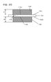
Classifications
-
- C—CHEMISTRY; METALLURGY
- C04—CEMENTS; CONCRETE; ARTIFICIAL STONE; CERAMICS; REFRACTORIES
- C04B—LIME, MAGNESIA; SLAG; CEMENTS; COMPOSITIONS THEREOF, e.g. MORTARS, CONCRETE OR LIKE BUILDING MATERIALS; ARTIFICIAL STONE; CERAMICS; REFRACTORIES; TREATMENT OF NATURAL STONE
- C04B35/00—Shaped ceramic products characterised by their composition; Ceramics compositions; Processing powders of inorganic compounds preparatory to the manufacturing of ceramic products
- C04B35/622—Forming processes; Processing powders of inorganic compounds preparatory to the manufacturing of ceramic products
- C04B35/64—Burning or sintering processes
- C04B35/645—Pressure sintering
-
- C—CHEMISTRY; METALLURGY
- C04—CEMENTS; CONCRETE; ARTIFICIAL STONE; CERAMICS; REFRACTORIES
- C04B—LIME, MAGNESIA; SLAG; CEMENTS; COMPOSITIONS THEREOF, e.g. MORTARS, CONCRETE OR LIKE BUILDING MATERIALS; ARTIFICIAL STONE; CERAMICS; REFRACTORIES; TREATMENT OF NATURAL STONE
- C04B37/00—Joining burned ceramic articles with other burned ceramic articles or other articles by heating
- C04B37/02—Joining burned ceramic articles with other burned ceramic articles or other articles by heating with metallic articles
- C04B37/023—Joining burned ceramic articles with other burned ceramic articles or other articles by heating with metallic articles characterised by the interlayer used
- C04B37/025—Joining burned ceramic articles with other burned ceramic articles or other articles by heating with metallic articles characterised by the interlayer used consisting of glass or ceramic material
-
- H—ELECTRICITY
- H05—ELECTRIC TECHNIQUES NOT OTHERWISE PROVIDED FOR
- H05K—PRINTED CIRCUITS; CASINGS OR CONSTRUCTIONAL DETAILS OF ELECTRIC APPARATUS; MANUFACTURE OF ASSEMBLAGES OF ELECTRICAL COMPONENTS
- H05K1/00—Printed circuits
- H05K1/02—Details
- H05K1/0271—Arrangements for reducing stress or warp in rigid printed circuit boards, e.g. caused by loads, vibrations or differences in thermal expansion
-
- H—ELECTRICITY
- H05—ELECTRIC TECHNIQUES NOT OTHERWISE PROVIDED FOR
- H05K—PRINTED CIRCUITS; CASINGS OR CONSTRUCTIONAL DETAILS OF ELECTRIC APPARATUS; MANUFACTURE OF ASSEMBLAGES OF ELECTRICAL COMPONENTS
- H05K1/00—Printed circuits
- H05K1/02—Details
- H05K1/03—Use of materials for the substrate
- H05K1/0306—Inorganic insulating substrates, e.g. ceramic, glass
-
- H—ELECTRICITY
- H05—ELECTRIC TECHNIQUES NOT OTHERWISE PROVIDED FOR
- H05K—PRINTED CIRCUITS; CASINGS OR CONSTRUCTIONAL DETAILS OF ELECTRIC APPARATUS; MANUFACTURE OF ASSEMBLAGES OF ELECTRICAL COMPONENTS
- H05K1/00—Printed circuits
- H05K1/18—Printed circuits structurally associated with non-printed electric components
- H05K1/181—Printed circuits structurally associated with non-printed electric components associated with surface mounted components
-
- H—ELECTRICITY
- H10—SEMICONDUCTOR DEVICES; ELECTRIC SOLID-STATE DEVICES NOT OTHERWISE PROVIDED FOR
- H10W—GENERIC PACKAGES, INTERCONNECTIONS, CONNECTORS OR OTHER CONSTRUCTIONAL DETAILS OF DEVICES COVERED BY CLASS H10
- H10W40/00—Arrangements for thermal protection or thermal control
- H10W40/20—Arrangements for cooling
- H10W40/22—Arrangements for cooling characterised by their shape, e.g. having conical or cylindrical projections
-
- H—ELECTRICITY
- H10—SEMICONDUCTOR DEVICES; ELECTRIC SOLID-STATE DEVICES NOT OTHERWISE PROVIDED FOR
- H10W—GENERIC PACKAGES, INTERCONNECTIONS, CONNECTORS OR OTHER CONSTRUCTIONAL DETAILS OF DEVICES COVERED BY CLASS H10
- H10W40/00—Arrangements for thermal protection or thermal control
- H10W40/20—Arrangements for cooling
- H10W40/25—Arrangements for cooling characterised by their materials
- H10W40/255—Arrangements for cooling characterised by their materials having a laminate or multilayered structure, e.g. direct bond copper [DBC] ceramic substrates
-
- H—ELECTRICITY
- H10—SEMICONDUCTOR DEVICES; ELECTRIC SOLID-STATE DEVICES NOT OTHERWISE PROVIDED FOR
- H10W—GENERIC PACKAGES, INTERCONNECTIONS, CONNECTORS OR OTHER CONSTRUCTIONAL DETAILS OF DEVICES COVERED BY CLASS H10
- H10W42/00—Arrangements for protection of devices
- H10W42/121—Arrangements for protection of devices protecting against mechanical damage
-
- H—ELECTRICITY
- H10—SEMICONDUCTOR DEVICES; ELECTRIC SOLID-STATE DEVICES NOT OTHERWISE PROVIDED FOR
- H10W—GENERIC PACKAGES, INTERCONNECTIONS, CONNECTORS OR OTHER CONSTRUCTIONAL DETAILS OF DEVICES COVERED BY CLASS H10
- H10W70/00—Package substrates; Interposers; Redistribution layers [RDL]
- H10W70/20—Conductive package substrates serving as an interconnection, e.g. metal plates
-
- H—ELECTRICITY
- H10—SEMICONDUCTOR DEVICES; ELECTRIC SOLID-STATE DEVICES NOT OTHERWISE PROVIDED FOR
- H10W—GENERIC PACKAGES, INTERCONNECTIONS, CONNECTORS OR OTHER CONSTRUCTIONAL DETAILS OF DEVICES COVERED BY CLASS H10
- H10W70/00—Package substrates; Interposers; Redistribution layers [RDL]
- H10W70/60—Insulating or insulated package substrates; Interposers; Redistribution layers
- H10W70/62—Insulating or insulated package substrates; Interposers; Redistribution layers characterised by their interconnections
- H10W70/65—Shapes or dispositions of interconnections
-
- H—ELECTRICITY
- H10—SEMICONDUCTOR DEVICES; ELECTRIC SOLID-STATE DEVICES NOT OTHERWISE PROVIDED FOR
- H10W—GENERIC PACKAGES, INTERCONNECTIONS, CONNECTORS OR OTHER CONSTRUCTIONAL DETAILS OF DEVICES COVERED BY CLASS H10
- H10W70/00—Package substrates; Interposers; Redistribution layers [RDL]
- H10W70/60—Insulating or insulated package substrates; Interposers; Redistribution layers
- H10W70/67—Insulating or insulated package substrates; Interposers; Redistribution layers characterised by their insulating layers or insulating parts
- H10W70/69—Insulating materials thereof
-
- C—CHEMISTRY; METALLURGY
- C04—CEMENTS; CONCRETE; ARTIFICIAL STONE; CERAMICS; REFRACTORIES
- C04B—LIME, MAGNESIA; SLAG; CEMENTS; COMPOSITIONS THEREOF, e.g. MORTARS, CONCRETE OR LIKE BUILDING MATERIALS; ARTIFICIAL STONE; CERAMICS; REFRACTORIES; TREATMENT OF NATURAL STONE
- C04B2237/00—Aspects relating to ceramic laminates or to joining of ceramic articles with other articles by heating
- C04B2237/02—Aspects relating to interlayers, e.g. used to join ceramic articles with other articles by heating
- C04B2237/12—Metallic interlayers
- C04B2237/125—Metallic interlayers based on noble metals, e.g. silver
-
- C—CHEMISTRY; METALLURGY
- C04—CEMENTS; CONCRETE; ARTIFICIAL STONE; CERAMICS; REFRACTORIES
- C04B—LIME, MAGNESIA; SLAG; CEMENTS; COMPOSITIONS THEREOF, e.g. MORTARS, CONCRETE OR LIKE BUILDING MATERIALS; ARTIFICIAL STONE; CERAMICS; REFRACTORIES; TREATMENT OF NATURAL STONE
- C04B2237/00—Aspects relating to ceramic laminates or to joining of ceramic articles with other articles by heating
- C04B2237/02—Aspects relating to interlayers, e.g. used to join ceramic articles with other articles by heating
- C04B2237/12—Metallic interlayers
- C04B2237/126—Metallic interlayers wherein the active component for bonding is not the largest fraction of the interlayer
- C04B2237/127—The active component for bonding being a refractory metal
-
- C—CHEMISTRY; METALLURGY
- C04—CEMENTS; CONCRETE; ARTIFICIAL STONE; CERAMICS; REFRACTORIES
- C04B—LIME, MAGNESIA; SLAG; CEMENTS; COMPOSITIONS THEREOF, e.g. MORTARS, CONCRETE OR LIKE BUILDING MATERIALS; ARTIFICIAL STONE; CERAMICS; REFRACTORIES; TREATMENT OF NATURAL STONE
- C04B2237/00—Aspects relating to ceramic laminates or to joining of ceramic articles with other articles by heating
- C04B2237/30—Composition of layers of ceramic laminates or of ceramic or metallic articles to be joined by heating, e.g. Si substrates
- C04B2237/32—Ceramic
- C04B2237/36—Non-oxidic
- C04B2237/368—Silicon nitride
-
- C—CHEMISTRY; METALLURGY
- C04—CEMENTS; CONCRETE; ARTIFICIAL STONE; CERAMICS; REFRACTORIES
- C04B—LIME, MAGNESIA; SLAG; CEMENTS; COMPOSITIONS THEREOF, e.g. MORTARS, CONCRETE OR LIKE BUILDING MATERIALS; ARTIFICIAL STONE; CERAMICS; REFRACTORIES; TREATMENT OF NATURAL STONE
- C04B2237/00—Aspects relating to ceramic laminates or to joining of ceramic articles with other articles by heating
- C04B2237/30—Composition of layers of ceramic laminates or of ceramic or metallic articles to be joined by heating, e.g. Si substrates
- C04B2237/40—Metallic
- C04B2237/407—Copper
-
- C—CHEMISTRY; METALLURGY
- C04—CEMENTS; CONCRETE; ARTIFICIAL STONE; CERAMICS; REFRACTORIES
- C04B—LIME, MAGNESIA; SLAG; CEMENTS; COMPOSITIONS THEREOF, e.g. MORTARS, CONCRETE OR LIKE BUILDING MATERIALS; ARTIFICIAL STONE; CERAMICS; REFRACTORIES; TREATMENT OF NATURAL STONE
- C04B2237/00—Aspects relating to ceramic laminates or to joining of ceramic articles with other articles by heating
- C04B2237/50—Processing aspects relating to ceramic laminates or to the joining of ceramic articles with other articles by heating
- C04B2237/70—Forming laminates or joined articles comprising layers of a specific, unusual thickness
- C04B2237/704—Forming laminates or joined articles comprising layers of a specific, unusual thickness of one or more of the ceramic layers or articles
-
- C—CHEMISTRY; METALLURGY
- C04—CEMENTS; CONCRETE; ARTIFICIAL STONE; CERAMICS; REFRACTORIES
- C04B—LIME, MAGNESIA; SLAG; CEMENTS; COMPOSITIONS THEREOF, e.g. MORTARS, CONCRETE OR LIKE BUILDING MATERIALS; ARTIFICIAL STONE; CERAMICS; REFRACTORIES; TREATMENT OF NATURAL STONE
- C04B2237/00—Aspects relating to ceramic laminates or to joining of ceramic articles with other articles by heating
- C04B2237/50—Processing aspects relating to ceramic laminates or to the joining of ceramic articles with other articles by heating
- C04B2237/70—Forming laminates or joined articles comprising layers of a specific, unusual thickness
- C04B2237/706—Forming laminates or joined articles comprising layers of a specific, unusual thickness of one or more of the metallic layers or articles
-
- C—CHEMISTRY; METALLURGY
- C04—CEMENTS; CONCRETE; ARTIFICIAL STONE; CERAMICS; REFRACTORIES
- C04B—LIME, MAGNESIA; SLAG; CEMENTS; COMPOSITIONS THEREOF, e.g. MORTARS, CONCRETE OR LIKE BUILDING MATERIALS; ARTIFICIAL STONE; CERAMICS; REFRACTORIES; TREATMENT OF NATURAL STONE
- C04B2237/00—Aspects relating to ceramic laminates or to joining of ceramic articles with other articles by heating
- C04B2237/50—Processing aspects relating to ceramic laminates or to the joining of ceramic articles with other articles by heating
- C04B2237/86—Joining of two substrates at their largest surfaces, one surface being complete joined and covered, the other surface not, e.g. a small plate joined at it's largest surface on top of a larger plate
-
- H—ELECTRICITY
- H05—ELECTRIC TECHNIQUES NOT OTHERWISE PROVIDED FOR
- H05K—PRINTED CIRCUITS; CASINGS OR CONSTRUCTIONAL DETAILS OF ELECTRIC APPARATUS; MANUFACTURE OF ASSEMBLAGES OF ELECTRICAL COMPONENTS
- H05K2201/00—Indexing scheme relating to printed circuits covered by H05K1/00
- H05K2201/06—Thermal details
- H05K2201/068—Thermal details wherein the coefficient of thermal expansion is important
Definitions
- the present invention relates to a ceramic circuit board and an electronic device.
- a ceramic circuit board suitable as an insulating substrate for a power semiconductor such as a bipolar transistor, a power MOSFET (metal-oxide-semiconductor field-effect transistor), and an IGBT (Insulated Gate Bipolar Transistor).
- a power semiconductor such as a bipolar transistor, a power MOSFET (metal-oxide-semiconductor field-effect transistor), and an IGBT (Insulated Gate Bipolar Transistor).
- IGBT Insulated Gate Bipolar Transistor
- a ceramic circuit board 100 having a first metal plate 104 on the front surface 102a of the ceramic substrate 102 and a second metal plate 106 on the back surface 102b of the ceramic substrate 102 has been developed. It is used as a semiconductor insulating substrate (see, for example, Japanese Patent No. 3847954). Then, the electronic device 112 is configured by mounting the power semiconductor 108 on the first metal plate 104 via the solder layer 110, for example.
- the ceramic circuit board 100 on which the power semiconductor 108 is mounted is required to have high heat dissipation in order to suppress heat generation. Therefore, generally, the first metal plate 104 and the second metal plate 106 are metal plates having high thermal conductivity such as Cu (copper) and Al (aluminum).
- the ceramic substrate 102 a ceramic substrate having a high thermal conductivity such as AlN (aluminum nitride) or Si 3 N 4 (silicon nitride) is selected.
- a heat dissipating board obtained by directly joining these members or joining them via a brazing material is used as the ceramic circuit board 100.
- the first metal plate 104 and the second metal plate 106 made of Cu and the ceramic substrate 102 made of Si 3 N 4 are joined through a brazing material such as Ag (silver) -Cu brazing.
- a brazing material such as Ag (silver) -Cu brazing.
- the ceramic circuit board 100 is made of ceramic having high strength and Cu having high thermal conductivity, it has excellent thermal cycle characteristics and is preferably used.
- a heat sink is bonded to the end surface of the second metal plate 106.
- the ceramic circuit board 100 needs to have further heat dissipation.
- the thermal stress caused by the difference in thermal expansion between the first metal plate 104 and the ceramic substrate 102 is caused by the thermal cycle during use. It occurs at the interface 114a with the ceramic substrate 102.
- the surface 102a of the ceramic substrate 102 is in a state where the above-described interface 114a to which thermal stress is applied and a peripheral portion to which no thermal stress is applied are mixed.
- thermal stress accompanying the difference in thermal expansion between the second metal plate 106 and the ceramic substrate 102 is generated at the interface 114b between the second metal plate 106 and the ceramic substrate 102.
- the back surface 102b of the ceramic substrate 102 is in a state where the above-described interface 114b to which thermal stress is applied and a peripheral portion to which no thermal stress is applied are mixed.
- the conventional ceramic circuit board 100 has a problem that the heat dissipation cannot be improved and the above-described needs cannot be met.
- An object of the present invention is to provide a ceramic circuit board and an electronic device that can suppress the occurrence of warpage and can improve heat dissipation.
- a ceramic circuit board according to a first aspect of the present invention is bonded to a ceramic substrate, a metal plate (referred to as a first metal plate) bonded to the surface of the ceramic substrate, and a surface side of the first metal plate.
- the member is made of a material having a smaller coefficient of thermal expansion than that of the metal plate and a large Young's modulus.
- thermal stress is generated at the interface 1 between the first metal plate and the ceramic substrate, and compressive stress or tensile stress is applied intensively at the boundary portion between the interface 1 and the peripheral portion of the surface of the ceramic substrate.
- the thermal stress shown in (i) is alleviated (reduced) particularly by the generation of the thermal stress shown in (ii). That is, the thermal stress due to the thermal cycle is generated by being distributed between the interface 1 and the interface 2, and the compressive stress and the tensile stress that are concentrated on the boundary portion between the interface 1 and the peripheral portion of the surface of the ceramic substrate. Is alleviated and there is no risk of cracking or cracking in the ceramic substrate due to the thermal cycle during use. Thereby, it becomes possible to enlarge the thickness of a 1st metal plate, and can aim at the improvement of heat dissipation.
- the member may be formed in an annular shape along the outer periphery of the surface of the first metal plate.
- a plurality of the members may be arranged along the outer periphery of the surface of the first metal plate.
- the two members may be joined to a line-symmetric position.
- a part of the member may protrude laterally from the outer periphery of the surface of the first metal plate.
- alignment when joining a member to the surface of the first metal plate is easy, and man-hours can be reduced, yield can be improved, and productivity can be improved.
- the entire member may be bonded to the surface of the first metal plate.
- the amount of the constituent material of the member can be reduced, and the manufacturing cost can be reduced.
- a recess may be formed in a part of the surface of the first metal plate, and the member may be joined to the recess.
- the mountability of the power semiconductor can be improved.
- the member and the ceramic substrate those having at least physical properties and thickness adjusted so as to suppress warpage of the ceramic circuit substrate are used. preferable. This can be achieved by adjusting the respective thicknesses from the thermal expansion coefficient and Young's modulus of the member and the ceramic substrate. For example, when the Young's modulus of the member is equal to that of the ceramic substrate, the thickness of the member is made thinner than that of the ceramic substrate if the coefficient of thermal expansion of the member is smaller than that of the ceramic substrate.
- the constituent material of the member is preferably a ceramic material similar to the ceramic substrate.
- the constituent material of the ceramic substrate is preferably silicon nitride.
- Silicon nitride is suitably used because it has not only high thermal conductivity, but also high “strength” and “toughness”, and high resistance to cracks and cracks in the ceramic substrate due to thermal cycling.
- another metal plate (hereinafter referred to as a second metal plate) is joined to the back surface of the ceramic substrate, and the thickness of the first metal plate is greater than the thickness of the second metal plate. Is also preferably large.
- the thermal stress to the interface 1 is relaxed, even if the thickness of the second metal plate is smaller than the thickness of the first metal plate, the occurrence of warpage of the entire ceramic circuit board is suppressed, There is no risk of cracking in the power semiconductor soldered on the surface of the ceramic circuit board or cracking in the bonding layer. As a result, the heat dissipation can be improved, and it is advantageous for reducing the height (thinning) of the ceramic circuit board.
- the thickness of the ceramic substrate is ta
- the thickness of the first metal plate is t1
- the thickness of the second metal plate is t2, t2 ⁇ ta ⁇ t1 It may be.
- An electronic device includes the above-described ceramic circuit board according to the first aspect of the present invention and a power semiconductor mounted on the surface of the first metal plate of the ceramic circuit board. It is characterized by.
- the thermal stress generated at the interface between the metal plate and the ceramic substrate is alleviated even if the thickness of the metal plate on which the power semiconductor is mounted is increased.
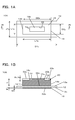
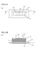
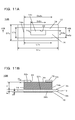
- FIG. 1A is a plan view showing a ceramic circuit board (first ceramic circuit board) according to the first embodiment as viewed from above, and FIG. 1B is a cross-sectional view taken along the line IB-IB in FIG. 1A.
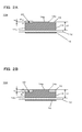
- FIG. 2A is a longitudinal sectional view showing a form in which the depth of the depression is shallower than the thickness of the member in the first ceramic circuit board, and FIG. 2B is a form in which the depth of the depression is deeper than the thickness of the member in the first ceramic circuit board.
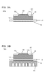
- FIG. FIG. 3A is a longitudinal sectional view showing an electronic device (first electronic device) according to the first embodiment, and FIG. 3B is a longitudinal sectional view showing another example of the first electronic device.
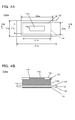
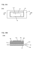
- FIG. 4A is a plan view showing a first modification of the first ceramic circuit board as viewed from above, and FIG. 4B is a cross-sectional view taken along the line IVB-IVB in FIG. 4A.
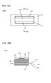
- FIG. 5A is a plan view showing a second modification of the first ceramic circuit board as viewed from above, and FIG. 5B is a cross-sectional view taken along the line VB-VB in FIG. 5A.
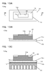
- FIG. 6A is a plan view showing a third modification of the first ceramic circuit board as viewed from above, and FIG. 6B is a cross-sectional view taken along the line VIB-VIB in FIG. 6A.
- FIG. 7A is a plan view showing a fourth modification of the first ceramic circuit board as viewed from above, and FIG.
- FIG. 7B is a cross-sectional view taken along the line VIIB-VIIB in FIG. 7A.
- FIG. 8A is a plan view showing a fifth modification of the first ceramic circuit board as viewed from above, and FIG. 8B is a cross-sectional view taken along the line VIIIB-VIIIB in FIG. 8A.
- FIG. 9A is a plan view showing a sixth modification of the first ceramic circuit board as viewed from above, and FIG. 9B is a cross-sectional view taken along the line IXB-IXB in FIG. 9A.
- FIG. 10A is a plan view showing a seventh modification of the first ceramic circuit board as viewed from above, FIG. 10B is a cross-sectional view taken along the line XB-XB in FIG.
- FIG. 10A is a longitudinal cross-sectional view which shows the example joined by pinching
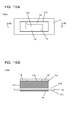
- FIG. 11A is a plan view showing a ceramic circuit board (second ceramic circuit board) according to the second embodiment as viewed from above, and FIG. 11B is a cross-sectional view taken along line XIB-XIB in FIG. 11A.
- 12A is a plan view showing a first modification of the second ceramic circuit board as viewed from above, and FIG. 12B is a cross-sectional view taken along the line XIIB-XIIB in FIG. 12A.
- FIG. 11A is a plan view showing a ceramic circuit board (second ceramic circuit board) according to the second embodiment as viewed from above
- FIG. 11B is a cross-sectional view taken along line XIB-XIIB in FIG. 11A.
- FIG. 12A is a plan view showing a first modification of the second ceramic circuit board as viewed
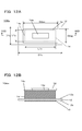
- FIG. 13A is a plan view showing a second modification of the second ceramic circuit board as viewed from above, and FIG. 13B is a cross-sectional view taken along line XIIIB-XIIIB in FIG. 13A.
- FIG. 14A is a plan view showing a third modification of the second ceramic circuit board as viewed from above, and FIG. 14B is a cross-sectional view taken along the line XIVB-XIVB in FIG. 14A.
- FIG. 15A is a plan view showing a fourth modification of the second ceramic circuit board as seen from above, and FIG. 15B is a cross-sectional view taken along the line XVB-XVB in FIG. 15A.
- FIG. 16A is a plan view showing a fifth modification of the second ceramic circuit board as viewed from above, and FIG. 16B is a cross-sectional view taken along the line XVIB-XVIB in FIG. 16A.
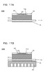
- FIG. 17A is a longitudinal sectional view showing an electronic device (second electronic device) according to the second embodiment, and FIG. 17B is a longitudinal sectional view showing another example of the second electronic device.
- 18A is a plan view showing a sixth modification of the second ceramic circuit board as viewed from above, FIG. 18B is a cross-sectional view taken along the line XVIIIB-XVIIIB in FIG. 18A, and FIG. 18C is a view between the ceramic board and the heat sink.
- FIG. 19A is a longitudinal sectional view showing a ceramic circuit board according to a conventional example
- FIG. 19B is a longitudinal sectional view showing a state where a power semiconductor is mounted on a first metal plate via a solder layer. It is explanatory drawing which shows the problem at the time of increasing the thickness of a 1st metal plate and a 2nd metal plate in the ceramic circuit board which concerns on a prior art example.
- ⁇ indicating a numerical range is used as a meaning including numerical values described before and after the numerical value as a lower limit value and an upper limit value.
- a ceramic circuit board (hereinafter referred to as a first ceramic circuit board 10A) according to the first embodiment includes a ceramic board 12 and a surface 12a of the ceramic board 12 as shown in FIGS. 1A and 1B.
- the first metal plate 14 bonded to the first metal plate 14, the second metal plate 16 bonded to the back surface 12 b of the ceramic substrate 12, and the member 18 bonded to the front surface 14 a side of the first metal plate 14.
- the member 18 is made of a material having a smaller coefficient of thermal expansion than that of the first metal plate 14 and a large Young's modulus.
- the 1st metal plate 14 and the 2nd metal plate 16 can be comprised with a metal plate of high thermal conductivity including Cu (copper) and Al (aluminum).
- the ceramic substrate 12 can be made of a ceramic material having a high thermal conductivity such as AlN (aluminum nitride) or Si 3 N 4 (silicon nitride).
- the bonding between the first metal plate 14 and the ceramic substrate 12 and the bonding between the second metal plate 16 and the ceramic substrate 12 may be direct bonding or may be bonded via a brazing material.
- a brazing material obtained by adding an active metal such as Ti (titanium) to a brazing material such as an Ag—Cu brazing material can be used. Specific constituent materials and joining of the member 18 will be described later.
- this 1st ceramic circuit board 10A has the hollow 20 in a part of surface 14a of the 1st metal plate 14, and the member 18 is embedded in the hollow 20 and joined.
- the “front surface 14a of the first metal plate 14” refers to a surface (for example, the upper surface in FIG. 1B) on which the power semiconductor 26 (see FIG. 3A) is mounted
- the back surface refers to a surface facing the front surface 14a ( For example, it refers to the lower surface in FIG. 1B.
- the surface of another member such as the ceramic substrate 12 also refers to the surface on which the power semiconductor 26 is mounted (for example, the upper surface in FIG. 1B), and the back surface of the other member is also the surface facing the surface (for example, the lower surface in FIG. 1B). ).
- the recess 20 is formed in an annular shape along the outer periphery 14 c of the surface 14 a of the first metal plate 14.
- the outer periphery 14 c of the surface 14 a of the first metal plate 14 is Part of it. That is, the recess 20 is formed from the surface 14 a to the side surface 14 b of the first metal plate 14. Therefore, the first metal plate 14 has a shape in which a shoulder portion is notched by the recess 20.
- the member 18 is constituted by one annular member along the annular shape of the recess 20. That is, the member 18 is joined so as to fill the recess 20 of the first metal plate 14.
- the member 18 is preferably joined from the bottom surface 20a to the side surface 20b of the recess 20 by a brazing material such as an Ag—Cu brazing material.
- each of the ceramic substrate 12, the first metal plate 14, and the second metal plate 16 may be various shapes.
- each of the outer shapes is a rectangular shape as viewed from above.
- the length D1y in the vertical direction and the length D1x in the horizontal direction when the ceramic substrate 12 is viewed from the top are set longer than the length L1y in the vertical direction and the length L1x in the horizontal direction of the first metal plate 14.
- the length in the vertical direction and the length in the horizontal direction of the first metal plate 14 and the second metal plate 16 are substantially the same.
- a rectangular hole 22 is also formed in the center of the member 18, and the surface 14 a of the first metal plate 14 is exposed through the hole 22.
- the relationship between the longitudinal length D2y and the lateral length D2x of the member 18 as viewed from above and the longitudinal length L1y and the lateral length L1x of the first metal plate 14 is any of the following relationships: May be adopted.
- D2y L1y, D2x> L1x (A-5) D2y> L1y, D2x> L1x (A-6) D2y ⁇ L1y, D2x> L1x (A-7)
- D2y L1y, D2x ⁇ L1x (A-8) D2y> L1y, D2x ⁇ L1x (A-9) D2y ⁇ L1y, D2x ⁇ L1x (A-9) D2y ⁇ L1y, D2
- (A-1) is the above-described first ceramic circuit board 10A (see FIGS. 1A and 1B).
- Each external shape of the ceramic substrate 12, the first metal plate 14, and the second metal plate 16 is not only the above-described rectangular shape but also a polygonal shape such as a circular shape, an elliptical shape, a track shape, a triangular shape, a pentagonal shape, and a hexagonal shape. Can be mentioned.
- the thickness of the ceramic substrate 12 when the thickness of the ceramic substrate 12 is ta, the thickness of the member 18 is tb, the thickness of the first metal plate 14 is t1, and the thickness of the second metal plate 16 is t2, ta ⁇ tb t2 ⁇ ta ⁇ t1 It has become.
- the depth tc of the recess 20 may be the same as the thickness tb of the member 18 as shown in FIG. 1B, or may be shallower than the thickness tb of the member 18 as shown in FIG. 2A. Alternatively, as shown in FIG. 2B, the thickness may be deeper than the thickness tb of the member 18.
- the power semiconductor 26 is mounted on the surface 14a of the first metal plate 14 via the bonding layer 24 such as solder, so that the electronic device according to the first embodiment (hereinafter, referred to as the electronic device) ,
- the first electronic device 28A) is configured.
- the first electronic device 28 ⁇ / b> A may be configured by further joining the heat sink 30 to the end face of the second metal plate 16.
- the height of the power semiconductor 26 is shown to be smaller than the thickness of the member 18, but the present invention is not limited to this.
- the member 18 is joined to the recess 20 formed on the surface 14a of the first metal plate 14, the following thermal stress is generated by the thermal cycle during use.
- the thermal stress accompanying the thermal expansion difference between the first metal plate 14 and the ceramic substrate 12 is generated at the interface 32a between the first metal plate 14 and the ceramic substrate 12 (hereinafter referred to as the first interface 32a).
- thermal stress has been concentrated on the first interface 32a between the first metal plate 14 and the ceramic substrate 12, but in the present embodiment, in particular, due to the generation of thermal stress shown in (c),
- the thermal stress shown in (a) is relaxed (reduced). That is, the thermal stress due to the thermal cycle is generated by being dispersed in the first interface 32a and the third interface 32c.
- the compressive stress and tensile stress concentrated on the boundary portion between the first interface 32a and the peripheral portion thereof are alleviated, and cracks in the ceramic substrate 12 due to the thermal cycle during use. There is no risk of cracking or cracking. Thereby, it becomes possible to enlarge thickness t1 of the 1st metal plate 14, and can aim at the improvement of heat dissipation.
- the thermal stress to the first interface 32a is relaxed, even if the thickness t2 of the second metal plate 16 is smaller than the thickness t1 of the first metal plate 14, the warp of the entire first ceramic circuit board 10A.
- the occurrence of cracks in the soldered power semiconductor 26 and the occurrence of cracks in the bonding layer 24 are eliminated.
- the distance from the ceramic substrate 12 to the heat sink 30 can be shortened, heat dissipation can be improved, and the first ceramic circuit substrate 10A can be reduced in height (thinned).
- the surface on which the power semiconductor 26 is mounted is substantially the same as the surface of the member 18 or higher than the surface of the member 18, the mountability of the power semiconductor 26 is improved. be able to.
- the member 18 and the ceramic substrate 12 that have at least physical properties and thickness adjusted so as to suppress the warpage of the first ceramic circuit substrate 10A.
- This can be achieved by adjusting the respective thicknesses from the thermal expansion coefficient and Young's modulus of the member 18 and the ceramic substrate 12. For example, when the Young's modulus of the member 18 and the ceramic substrate 12 are equal, if the coefficient of thermal expansion of the member 18 is smaller than that of the ceramic substrate 12, the thickness of the member 18 is made thinner than that of the ceramic substrate 12.
- the constituent material of the member 18 and the ceramic substrate 12 may be the same, for example, the constituent material of the member 18 may be ceramic.
- the member 18 is also Si 3 N 4 .
- Si 3 N 4 is preferably used because it has not only high thermal conductivity but also high “strength” and “toughness” and high resistance to cracks and cracks in the ceramic substrate 12 due to thermal cycling.
- Preferred constituent materials of the member 18 include ceramics, semiconductors, metals, and the like.
- the ceramic include Si 3 N 4 , AlN, Al 2 O 3 , SiC (silicon carbide), cordierite, mullite, and the like
- the semiconductor include Si (silicon), GaN (gallium nitride), and SiC.
- the metal include W (tungsten), Mo (molybdenum), Cr (chromium), Nb (niobium), Ir (iridium), and alloys (CuMo, CuW, etc.) containing these as a main component.
- the member 18 preferably has a thickness of 100 ⁇ m or more and 1 mm or less and a thermal expansion coefficient of 10 ppm / K or less.
- the Young's modulus is preferably larger than that of the first metal plate 14. If the first metal plate 14 is, for example, copper, 130 GPa or more is preferable. Generation of cracks in the bonding layer 24 and the ceramic substrate 12 in a thermal cycle described later can be effectively prevented. Moreover, if it is the material similar to the ceramic substrate 12, since the member 18 can be manufactured simultaneously when manufacturing the ceramic substrate 12, it is advantageous in terms of cost.
- brazing with Ag—Cu brazing or the like can be used if the constituent material of the member 18 is ceramic or semiconductor. If the constituent material of the member 18 is a metal material, not only brazing but also coating such as thermal spraying can be used.
- the first ceramic circuit board 10A and the first electronic device 28A even if the first metal plate 14 on the side where the power semiconductor 26 is mounted is thickened at least, the first metal plate 14 and the ceramic substrate 12 The thermal stress generated at the first interface 32a can be relieved, and the occurrence of warpage can be suppressed, so that the heat dissipation can be improved. Moreover, it is advantageous for downsizing.
- FIG. 4A and FIG. 4B show an example of (A-5) (first ceramic circuit board 10Aa according to the first modified example) shown in FIG. Shown in 4B.
- alignment when the member 18 is joined to the surface 14a of the first metal plate 14 is easy, and man-hours can be reduced, yield can be improved, and productivity can be improved.
- (A-3), (A-7), and (A-9) show examples in which the entire member 18 is joined to the bottom surface 20a of the recess 20, and typically (A-9) ) (First ceramic circuit board 10Ab according to a second modification) is shown in FIGS. 5A and 5B.
- the second modification the amount of the constituent material of the member 18 is small, and the manufacturing cost can be reduced.
- the first ceramic circuit board 10Ac according to the third modified example has substantially the same configuration as the first ceramic circuit board 10A.
- the annular recess 20 is formed by the first metal plate 14. It differs in that it is formed at a position inside the outer periphery 14c of the surface 14a.
- the first ceramic circuit boards 10Ad and 10Ae according to the fourth modification and the fifth modification have substantially the same configuration as the first ceramic circuit board 10A, but as shown in FIGS. 7A to 8B, a plurality of members 18 are provided. Are different in that they are arranged along the annular shape of the recess 20. In the fourth modification and the fifth modification, the member 18 is easily manufactured, and the man-hours can be reduced, the yield can be improved, and the productivity can be improved.
- the first ceramic circuit board 10Af according to the sixth modification has substantially the same configuration as that of the first ceramic circuit board 10A. However, as shown in FIGS. Formed in symmetrical positions, members 18 are joined to the respective depressions 20. In this case, the amount of the constituent material of the member 18 is small, and the manufacturing cost can be reduced.
- the first ceramic circuit board 10Ag according to the seventh modification has substantially the same configuration as the first ceramic circuit board 10A, but as shown in FIGS. 10A and 10B, a second metal plate is formed on the back surface 12b of the ceramic board 12. The difference is that 16 is not joined.
- the first ceramic circuit board 10Ag described above when the heat sink 30 is bonded to the back surface 12b of the ceramic substrate 12, the heat transfer grease is provided between the back surface 12b of the ceramic substrate 12 and the heat sink 30 as shown in FIG. 10C. Or TIM 17 or the like.
- the first ceramic circuit boards 10Aa to 10Ag according to the first to seventh modifications also have the same effects as the first ceramic circuit board 10A.
- second ceramic circuit board 10B a ceramic circuit board according to the second embodiment
- second electronic device 28B an electronic device according to the second embodiment
- the second ceramic circuit board 10B has substantially the same configuration as the first ceramic circuit board 10A described above, but as shown in FIGS. 11A and 11B, the surface 14a of the first metal plate 14 has no depression and is flat. The difference is that an annular member 18 is joined on the surface 14a (flat surface).
- the relationship between the length of the outer periphery (vertical length De2y and lateral length De2x) of the member 18 as viewed from above, and the longitudinal length L1y and lateral length L1x of the first metal plate 14 is as follows. Any of the following relationships may be adopted.
- (B-1) is the above-described second ceramic circuit board 10B (see FIGS. 11A and 11B).
- FIG. 12A and FIG. 12B show an example projecting in the lateral direction from 14c, and representatively, an example of (B-5) (second ceramic circuit board 10Ba according to the first modification) is shown.
- alignment when the member 18 is joined to the surface 14a of the first metal plate 14 is easy, and man-hours can be reduced, yield can be improved, and productivity can be improved.
- the examples of (B-3), (B-7), and (B-9) show examples in which the entire member 18 is joined into the surface 14a of the first metal plate 14, and typically ( FIG. 13A and FIG. 13B show an example of B-9) (second ceramic circuit board 10Bb according to the second modification).
- the second modification the amount of the constituent material of the member 18 is small, and the manufacturing cost can be reduced.
- the second ceramic circuit boards 10Bc and 10Bd according to the third and fourth modifications have substantially the same configuration as the first ceramic circuit board 10A, but as shown in FIGS. 14A to 15B, a plurality of members 18 are provided. Are different in that they are arranged along the outer periphery 14c of the surface 14a of the first metal plate 14. In the third and fourth modified examples, the member 18 is easily manufactured, and the number of man-hours, the yield can be improved, and the productivity can be improved.
- the second ceramic circuit board 10Be according to the fifth modification has a configuration in which some members 18 are removed from the third modification described above.
- FIG. 16A and FIG. 16B show an example in which two members 18 whose long sides extend in the same direction are joined (two members 18 that extend in a straight line are joined at positions that are axisymmetric).
- the amount of the constituent material of the member 18 can be small, and the manufacturing cost can be reduced.
- the 2nd electronic device 28B is exposed from the hole 22 of the member 18 among the surfaces 14a (flat surface) of the 1st metal plate 14, as shown to FIG. 17A similarly to the 1st electronic device 28A mentioned above.
- a power semiconductor 26 is mounted on the portion via a bonding layer 24 such as solder.
- the second electronic device 28 ⁇ / b> B may be configured by further joining the heat sink 30 to the end face of the second metal plate 16.
- the thickness t1 of the first metal plate 14 can be increased, and heat dissipation can be improved.
- the thickness t2 of the second metal plate 16 can be made smaller than the thickness t1 of the first metal plate 14, heat dissipation can be improved, and the second ceramic circuit board 10B can be reduced in height (thinned). ) Is also advantageous.
- second ceramic circuit substrate 10Bf a configuration in which the second metal plate 16 is not joined to the back surface 12b of the ceramic substrate 12 (second ceramic circuit substrate 10Bf according to the sixth modification) may be employed.
- the heat transfer grease is provided between the back surface 12b of the ceramic substrate 12 and the heat sink 30 as shown in FIG. 18C. Or TIM 17 or the like.
- the second ceramic circuit boards 10Ba to 10Bf according to the first to sixth modifications have the same effects as the second ceramic circuit board 10B.
- a silicon nitride (Si 3 N 4 ) substrate having a bending strength of 650 MPa and a thickness of 0.3 mm was prepared for the ceramic substrate 12 and the member 18.
- An oxygen-free Cu plate was prepared for the first metal plate 14 and the second metal plate 16.
- an Ag—Cu brazing material paste to which Ti active metal powder was added was prepared.
- Example 1 The ceramic circuit board of the evaluation sample according to Example 1 has the same configuration as the second ceramic circuit board 10B shown in FIGS. 11A and 11B. That is, an annular member 18 was used (indicated as “(annular)” in Table 1).
- first metal plate 14 and second metal plate 16 were joined.
- the thickness t1 of the first metal plate 14 was 2 mm
- the thickness t2 of the second metal plate 16 was 0.1 mm.
- the bonding conditions were heat and pressure bonding under vacuum at a temperature of 800 ° C. and 1 MPa.
- the power semiconductor 26 was joined by the joining layer 24 (in this case, a solder layer), and an evaluation sample according to Example 1 was obtained. Ten evaluation samples were produced.
- Example 2 The ceramic circuit board of the evaluation sample according to Example 2 has the same configuration as the ceramic circuit board 10Bc shown in FIGS. 14A and 14B. In other words, the same procedure as in Example 1 was performed except that the four members 18 were arrayed and joined along the outer periphery 14c of the surface 14a of the first metal plate 14 (indicated as “(Division 1)” in Table 1). Ten evaluation samples according to Example 2 were produced.
- Example 3 The ceramic circuit board of the evaluation sample according to Example 3 has the same configuration as the ceramic circuit board 10Be shown in FIGS. 16A and 16B. That is, 10 according to the third embodiment is the same as the first embodiment except that the two members 18 extending in a straight line are joined at line-symmetric positions (indicated as “(division 2)” in Table 1). Individual evaluation samples were prepared.
- Example 4 The ceramic circuit board of the evaluation sample according to Example 4 has the same configuration as the first ceramic circuit board 10A shown in FIGS. 1A and 1B. That is, the outer peripheral portion of the surface 14a of the first metal plate 14 is etched to form an annular recess 20, and the annular member 18 is embedded and joined to the recess 20 (indicated as "(embedded)" in Table 1). Except for the above, ten evaluation samples according to Example 4 were produced in the same manner as in Example 1.
- Example 5 The ceramic circuit board of the evaluation sample according to Example 5 has the same configuration as the ceramic circuit board 10Bf shown in FIGS. 18A and 18B. That is, ten evaluation samples according to Example 5 were produced in the same manner as in Example 1 except that the second metal plate 16 was not joined to the back surface 12b of the ceramic substrate 12.
- Comparative Example 1 The ceramic circuit board of the evaluation sample according to Comparative Example 1 has the same configuration as the ceramic circuit board 100 shown in FIG. That is, the member 18 is not joined to the first metal plate 104, and the thicknesses of the first metal plate 104 and the second metal plate 106 are both 2 mm. Individual evaluation samples were prepared.
- Comparative Example 2 The evaluation sample according to Comparative Example 2 was carried out except that the member 18 was not joined to the first metal plate 104, the thickness of the first metal plate 104 was 2 mm, and the thickness of the second metal plate 106 was 0.1 mm. Ten evaluation samples according to Comparative Example 2 were produced in the same manner as Example 1.
- the rate of occurrence of cracks in the bonding layer 24 is represented by the number of evaluation samples in which cracks occurred in the bonding layer 24 among the 10 evaluation samples, and the rate of occurrence of cracks in the ceramic substrate is 10
- the number of evaluation samples in which cracks occurred in the ceramic substrate 12 was expressed.
- Comparative Example 1 In contrast, in Comparative Example 1, no crack was generated in the bonding layer 24, but cracks were generated in the ceramic substrate 102 in seven of the ten evaluation samples. In Comparative Example 2, no crack was generated in the ceramic substrate 102, but a crack was generated in the bonding layer 24 in all ten evaluation samples.
- a silicon nitride (Si 3 N 4 ) substrate having a bending strength of 650 MPa and a thickness of 0.3 mm was prepared.
- the Si 3 N 4 substrate has a thermal expansion coefficient of 3.1 ppm / K and a Young's modulus of 330 GPa.
- An oxygen-free Cu plate was prepared for the first metal plate 14 and the second metal plate 16.
- the oxygen-free Cu plate has a thermal expansion coefficient of 16.5 ppm / K and a Young's modulus of 129.8 GPa.
- an Ag—Cu brazing material paste to which Ti active metal powder was added was prepared.
- Example 6 An alumina (Al 2 O 3 ) substrate having a thickness of 0.3 mm was prepared for the member 18.
- the Al 2 O 3 substrate has a thermal expansion coefficient of 7.2 ppm / K and a Young's modulus of 310 GPa.
- the ceramic circuit board of the evaluation sample which concerns on Example 6 has the structure similar to the 2nd ceramic circuit board 10B shown to FIG. 11A and FIG. 11B similarly to the 1st Example mentioned above. That is, an annular member 18 was used (indicated as “(annular arrangement)” in Table 2).
- first metal plate 14 and second metal plate 16 were joined.
- the thickness t1 of the first metal plate 14 was 2 mm
- the thickness t2 of the second metal plate 16 was 0.1 mm.
- the bonding conditions were heat and pressure bonding under vacuum at a temperature of 800 ° C. and 1 MPa.
- the power semiconductor 26 was joined by the joining layer 24 (in this case, a solder layer), and an evaluation sample according to Example 6 was obtained. Ten evaluation samples were produced.
- Example 7 Except that an alumina-zirconia (Al 2 O 3 —ZrO 2 ) substrate having a thickness of 0.3 mm was prepared for the member 18, 10 pieces according to Example 7 were prepared in the same manner as in Example 6 described above. An evaluation sample was prepared.
- the Al 2 O 3 —ZrO 2 substrate contains 80% by mass of Al 2 O 3 and 20% by mass of ZrO 2 .
- the coefficient of thermal expansion is 8.3 ppm / K and the Young's modulus is 380 GPa.
- Example 8 Ten evaluation samples according to Example 8 were produced in the same manner as in Example 6 described above except that a silicon carbide (SiC) substrate having a thickness of 0.3 mm was prepared for the member 18.
- the SiC substrate has a thermal expansion coefficient of 3.8 ppm / K and a Young's modulus of 390 GPa.
- Example 9 Ten evaluation samples according to Example 9 were produced in the same manner as in Example 6 except that a zirconia (ZrO 2 ) substrate having a thickness of 0.3 mm was prepared for the member 18.
- the ZrO 2 substrate has a thermal expansion coefficient of 10.5 ppm / K and a Young's modulus of 200 GPa.
- Example 10 Ten evaluation samples according to Example 10 were produced in the same manner as in Example 6 described above except that a silicon (Si) substrate having a thickness of 0.3 mm was prepared for the member 18.
- the Si substrate has a thermal expansion coefficient of 3.9 ppm / K and a Young's modulus of 190 GPa.
- Example 11 Ten evaluation samples according to Example 11 were produced in the same manner as in Example 6 described above except that a tungsten (W) substrate having a thickness of 0.3 mm was prepared for the member 18.
- the W substrate has a coefficient of thermal expansion of 4.3 ppm / K and a Young's modulus of 345 GPa.
- Example 12 Ten evaluation samples according to Example 12 were prepared in the same manner as in Example 6 except that a tungsten-copper (W—Cu) substrate having a thickness of 0.3 mm was prepared for the member 18. did.
- the W—Cu substrate contains 80% by mass of W and 20% by mass of Cu.
- the coefficient of thermal expansion is 8.3 ppm / K and the Young's modulus is 290 GPa.
- Example 9 cracks were generated in the bonding layer 24 and the ceramic substrate 12 in one evaluation sample among the ten evaluation samples, but this is a practically satisfactory level. Cracks occurred only in Example 9 because the thermal expansion coefficient of the ZrO 2 plate of Example 9 among Examples 6 to 12 is the thermal expansion coefficient of the first metal plate 14 (in this case, 16.5 ppm / K). This is considered to be the closest to.
- the ceramic circuit board and the electronic device according to the present invention are not limited to the above-described embodiments, and various configurations can be adopted without departing from the gist of the present invention.
Landscapes
- Engineering & Computer Science (AREA)
- Chemical & Material Sciences (AREA)
- Ceramic Engineering (AREA)
- Microelectronics & Electronic Packaging (AREA)
- Inorganic Chemistry (AREA)
- Materials Engineering (AREA)
- Manufacturing & Machinery (AREA)
- Structural Engineering (AREA)
- Organic Chemistry (AREA)
- Structure Of Printed Boards (AREA)
- Cooling Or The Like Of Semiconductors Or Solid State Devices (AREA)
- Ceramic Products (AREA)
- Physics & Mathematics (AREA)
- Geometry (AREA)
Abstract
本発明は、セラミック回路基板及び電子デバイスに関する。セラミック基板(12)と、該セラミック基板(12)の表面(12a)に接合された第1金属板(14)と、第1金属板(14)の表面側に接合された部材(18)と、を有する。部材(18)は、第1金属板(14)よりも熱膨張係数が小さく、且つ、ヤング率が大きい材料からなる。
Description
本発明は、セラミック回路基板及び電子デバイスに関し、例えばバイポーラトランジスタ、パワーMOSFET(metal-oxide-semiconductor field-effect transistor)、IGBT(Insulated Gate Bipolar Transistor)等のパワー半導体の絶縁基板として好適なセラミック回路基板と、該セラミック回路基板を用いた電子デバイスに関する。
近年、例えば図19A及び図19Bに示すように、セラミック基板102の表面102aに第1金属板104を有し、セラミック基板102の裏面102bに第2金属板106を有するセラミック回路基板100が、パワー半導体の絶縁基板として使用されている(例えば特許第3847954号公報参照)。そして、第1金属板104上に、パワー半導体108を例えば半田層110を介して実装することによって電子デバイス112が構成される。
パワー半導体108が実装されるセラミック回路基板100は、発熱を抑えるため、高放熱性が要求される。従って、一般に、第1金属板104及び第2金属板106は、Cu(銅)やAl(アルミニウム)を始めとする高熱伝導率の金属板が選ばれる。セラミック基板102には、AlN(窒化アルミニウム)やSi3N4(窒化珪素)のような高熱伝導率のセラミック基板が選ばれる。これらを直接接合、もしくは、ろう材を介して接合した放熱基板をセラミック回路基板100として用いている。
特に、Cuにて構成された第1金属板104及び第2金属板106とSi3N4にて構成されたセラミック基板102とを、Ag(銀)-Cuろう等のろう材を介して接合したセラミック回路基板100は、高い強度を持ったセラミック、高い熱伝導率を持ったCuということで、熱サイクル特性に優れ、好適に用いられている。なお、第2金属板106の端面には、例えばヒートシンクが接合される。
ところで、最近では、パワー半導体108の出力密度を向上させて小型化したい、もしくは放熱性を向上させて冷却系を簡素化したい、というニーズがある。パワー半導体108の出力密度を向上させると発熱量が増加し、冷却系を簡素化すると、放熱性が低下するため、上述のニーズに対応するには、セラミック回路基板100にさらなる放熱性が要求される。
そこで、放熱性を向上させる方法として、例えば図20に示すように、第1金属板104及び第2金属板106の厚みt1及びt2を従来の厚み(図19A参照)より厚くすることが考えられる。
通常、図19Aに示す従来のセラミック回路基板100を使用する場合、使用時の熱サイクルによって、第1金属板104とセラミック基板102との熱膨張差に伴う熱応力が、第1金属板104とセラミック基板102との界面114aにおいて発生する。この場合、セラミック基板102の表面102aは、熱応力がかかる上述の界面114aと、熱応力がかからない周辺部とが混在した状態となる。同様に、第2金属板106とセラミック基板102との熱膨張差に伴う熱応力が、第2金属板106とセラミック基板102との界面114bにおいて発生する。この場合も、セラミック基板102の裏面102bは、熱応力がかかる上述の界面114bと、熱応力がかからない周辺部とが混在した状態となる。
従って、図20に示すように、第1金属板104の厚みt1及び第2金属板106の厚みt2を厚くすると、第1金属板104及び第2金属板106の体積が大きくなることから、第1金属板104とセラミック基板102の界面114a並びに第2金属板106とセラミック基板102の界面114bで発生する熱応力も増大する。そのため、使用時の熱サイクルによってセラミック基板102にクラック116(亀裂)が入ったり、割れるという問題が生じるおそれがある。すなわち、セラミック基板102の表面のうち、熱応力がかかる界面と熱応力がかからない周辺部との境界部分において集中的に圧縮応力や引っ張り応力がかかり、該境界部分からクラック116(亀裂)が入るおそれがある。
このように、従来のセラミック回路基板100では、放熱性の向上を実現することができず、上述したニーズに対応することができないという問題がある。
本発明はこのような課題を考慮してなされたものであり、少なくともパワー半導体が実装される側の金属板を厚くしても、金属板とセラミック基板の界面で生じる熱応力を緩和することができると共に、反りの発生も抑制することができ、放熱性の向上を図ることができるセラミック回路基板及び電子デバイスを提供することを目的とする。
[1] 第1の本発明に係るセラミック回路基板は、セラミック基板と、前記セラミック基板の表面に接合された金属板(第1金属板と記す)と、前記第1金属板の表面側に接合された部材と、を有し、前記部材は、前記金属板よりも熱膨張係数が小さく、且つ、ヤング率が大きい材料からなることを特徴とする。
これにより、使用時における熱サイクルによって、以下の熱応力が発生することになる。
(i) 第1金属板とセラミック基板との熱膨張差に伴う熱応力が、第1金属板とセラミック基板との界面(以下、界面1と記す)において発生する。
(ii) 第1金属板と部材との熱膨張差に伴う熱応力が、第1金属板と部材との界面(以下、界面2と記す)において発生する。
従来では、第1金属板とセラミック基板との界面1に熱応力が発生し、セラミック基板の表面のうち、界面1とその周辺部との境界部分において集中的に圧縮応力や引っ張り応力がかかっていたが、本発明では、特に、(ii)に示す熱応力の発生によって、(i)に示す熱応力が緩和(低減)されることになる。すなわち、熱サイクルによる熱応力が界面1と界面2とに分散して発生することとなり、セラミック基板の表面のうち、界面1とその周辺部との境界部分に集中的にかかる圧縮応力や引っ張り応力が緩和され、使用時の熱サイクルによるセラミック基板への亀裂や割れの発生のおそれがなくなる。これにより、第1金属板の厚みを大きくすることが可能となり、放熱性の向上を図ることができる。
[2] 第1の本発明において、前記部材は、前記第1金属板の表面の外周に沿って環状に形成されていてもよい。
[3] 第1の本発明において、複数の前記部材が前記第1金属板の表面の外周に沿って配列されていてもよい。
[4] 第1の本発明において、2つの前記部材が線対称の位置に接合されていてもよい。
[5] 第1の本発明において、前記部材は、その一部が、前記第1金属板の表面の外周よりも横方向に張り出していてもよい。この場合、第1金属板の表面に部材を接合する際の位置合わせが容易であり、工数の低減、歩留りの向上、生産性の向上を図ることができる。
[6] 第1の本発明において、前記部材は、その全体が、前記第1金属板の表面内に接合されていてもよい。この場合、部材の構成材料の量が少なくて済み、製造コストの低減を図ることができる。
[7] 第1の本発明において、前記第1金属板の表面の一部に窪みを有し、前記部材は、前記窪みに接合されていてもよい。この場合、パワー半導体が実装される面(第1金属板の表面)が部材の表面とほぼ同じ、あるいは部材の表面よりも高くなるため、パワー半導体の実装性の向上を図ることができる。
[8] 第1の本発明において、前記部材と前記セラミック基板として、当該セラミック回路基板に反りが発生するのを抑制するように、少なくとも物性及び厚みが調整されたものが用いられていることが好ましい。これは、部材とセラミック基板の熱膨張係数、ヤング率から、それぞれの厚みを調整することによって達成することができる。例えば、部材とセラミック基板のヤング率が同等の場合、部材の熱膨張係数がセラミック基板よりも小さいのであれば、部材の厚みは、セラミック基板よりも薄くする。
[9] 前記部材の構成材料は、前記セラミック基板と同様のセラミック材料であることが好ましい。
[10] 第1の本発明において、前記セラミック基板の構成材料は窒化珪素であることが好ましい。窒化珪素は、熱伝導率が高いだけでなく、「強度」、「靱性」も高く、熱サイクルによるセラミック基板のクラック(亀裂)や割れに対する耐性が高いため好適に用いられる。
[11] 第1の本発明において、前記セラミック基板の裏面に別の金属板(以下、第2金属板と記す)が接合され、前記第1金属板の厚みは前記第2金属板の厚みよりも大きいことが好ましい。
上述したように、界面1への熱応力が緩和されることから、第2金属板の厚みを第1金属板の厚みよりも小さくしても、セラミック回路基板全体の反りの発生が抑制され、セラミック回路基板の表面上に半田付けされたパワー半導体への割れの発生や、接合層へのクラックの発生のおそれがなくなる。これにより、放熱性を向上させることができると共に、セラミック回路基板の低背化(薄型化)にも有利になる。
[12] この場合、前記セラミック基板の厚みをta、前記第1金属板の厚みをt1、前記第2金属板の厚みをt2としたとき、
t2<ta<t1
であってもよい。
t2<ta<t1
であってもよい。
[13] 第2の本発明に係る電子デバイスは、上述した第1の本発明に係るセラミック回路基板と、該セラミック回路基板の前記第1金属板の表面に実装されたパワー半導体とを有することを特徴とする。
以上説明したように、本発明に係るセラミック回路基板及び電子デバイスによれば、少なくともパワー半導体が実装される側の金属板を厚くしても、金属板とセラミック基板の界面で生じる熱応力を緩和することができると共に、反りの発生も抑制することができ、放熱性の向上を図ることができる。
以下、本発明に係るセラミック回路基板の実施の形態例を図1A~図18Cを参照しながら説明する。なお、本明細書において数値範囲を示す「~」は、その前後に記載される数値を下限値及び上限値として含む意味として使用される。
先ず、第1の本実施の形態に係るセラミック回路基板(以下、第1セラミック回路基板10Aと記す)は、図1A及び図1Bに示すように、セラミック基板12と、該セラミック基板12の表面12aに接合された第1金属板14と、セラミック基板12の裏面12bに接合された第2金属板16と、第1金属板14の表面14a側に接合された部材18とを有する。部材18は、第1金属板14よりも熱膨張係数が小さく、且つ、ヤング率が大きい材料から構成される。
第1金属板14及び第2金属板16は、Cu(銅)やAl(アルミニウム)を始めとする高熱伝導率の金属板にて構成することができる。セラミック基板12は、AlN(窒化アルミニウム)やSi3N4(窒化珪素)のような高熱伝導率のセラミック材料にて構成することができる。第1金属板14とセラミック基板12との接合、並びに第2金属板16とセラミック基板12との接合は、直接接合でもよいし、もしくは、ろう材を介して接合してもよい。ろう材としては、Ag-Cuろう等のろう材にTi(チタン)等の活性金属を添加したろう材を用いることができる。部材18の具体的な構成材料並びに接合については後述する。
そして、この第1セラミック回路基板10Aは、第1金属板14の表面14aの一部に窪み20を有し、窪み20に部材18が埋め込まれ接合されている。ここで、「第1金属板14の表面14a」とは、パワー半導体26(図3A参照)が実装される面(例えば図1Bでは上面)をいい、裏面とは、表面14aと対向する面(例えば図1Bでは下面)をいう。セラミック基板12等の他の部材の表面も、パワー半導体26が実装される側の面(例えば図1Bでは上面)を指し、他の部材の裏面も、表面と対向する面(例えば図1Bでは下面)をいう。
窪み20は、第1金属板14の表面14aの外周14cに沿って環状に形成され、特に、図1A及び図1Bの例では、第1金属板14の表面14aの外周14cは、窪み20の一部を構成している。つまり、窪み20は、第1金属板14の表面14aから側面14bにかけて形成されている。そのため、第1金属板14は、肩部分が窪み20によって切り欠かれた形状を有する。また、部材18は、窪み20の環状に沿った1つの環状部材にて構成されている。すなわち、第1金属板14の窪み20を埋めるように部材18が接合される。部材18は、窪み20の底面20aから側面20bにかけてAg-Cuろう等のろう材等によって接合されることが好ましい。
セラミック基板12、第1金属板14及び第2金属板16の各外形形状は、様々な形状が挙げられるが、図1Aでは、上面から見て、それぞれ長方形状とされている。セラミック基板12を上面から見た縦方向の長さD1y及び横方向の長さD1xは、第1金属板14の縦方向の長さL1y及び横方向の長さL1xよりも長く設定されている。第1金属板14と第2金属板16の縦方向の長さ及び横方向の長さはそれぞれほぼ同じとされている。部材18の中央部には、同じく長方形状の孔22が形成され、この孔22を通じて第1金属板14の表面14aが露出している。
部材18を上面から見た縦方向の長さD2y及び横方向の長さD2xと第1金属板14の縦方向の長さL1y及び横方向の長さL1xとの関係は、以下の関係のいずれを採用してもよい。
(A-1) D2y=L1y、D2x=L1x
(A-2) D2y>L1y、D2x=L1x
(A-3) D2y<L1y、D2x=L1x
(A-4) D2y=L1y、D2x>L1x
(A-5) D2y>L1y、D2x>L1x
(A-6) D2y<L1y、D2x>L1x
(A-7) D2y=L1y、D2x<L1x
(A-8) D2y>L1y、D2x<L1x
(A-9) D2y<L1y、D2x<L1x
(A-1) D2y=L1y、D2x=L1x
(A-2) D2y>L1y、D2x=L1x
(A-3) D2y<L1y、D2x=L1x
(A-4) D2y=L1y、D2x>L1x
(A-5) D2y>L1y、D2x>L1x
(A-6) D2y<L1y、D2x>L1x
(A-7) D2y=L1y、D2x<L1x
(A-8) D2y>L1y、D2x<L1x
(A-9) D2y<L1y、D2x<L1x
このうち、(A-1)の例が上述した第1セラミック回路基板10A(図1A及び図1B参照)である。
セラミック基板12、第1金属板14及び第2金属板16の各外形形状は、上述した長方形状のほか、円形状、楕円形状、トラック形状、三角形状、五角形、六角形等の多角形状等が挙げられる。
また、第1セラミック回路基板10Aは、セラミック基板12の厚みをta、部材18の厚みをtb、第1金属板14の厚みをt1、第2金属板16の厚みをt2としたとき、
ta≒tb
t2<ta<t1
となっている。
ta≒tb
t2<ta<t1
となっている。
窪み20の深さtcは、図1Bに示すように、部材18の厚みtbと同じでもよいし、図2Aに示すように、部材18の厚みtbより浅くてもよい。あるいは、図2Bに示すように、部材18の厚みtbより深くてもよい。
そして、図3Aに示すように、第1金属板14の表面14aに半田等の接合層24を介してパワー半導体26が実装されることで、第1の本実施の形態に係る電子デバイス(以下、第1電子デバイス28A)が構成される。もちろん、図3Bに示すように、さらに、第2金属板16の端面にヒートシンク30を接合して第1電子デバイス28Aを構成してもよい。なお、図3A及び図3B等では、パワー半導体26の高さを、部材18の厚みよりも薄く図示されているが、これに限定されるものではない。
この第1セラミック回路基板10Aにおいては、第1金属板14の表面14aに形成された窪み20に部材18を接合したので、使用時における熱サイクルによって、以下の熱応力が発生することになる。
(a) 第1金属板14とセラミック基板12との熱膨張差に伴う熱応力が、第1金属板14とセラミック基板12との界面32a(以下、第1界面32aと記す)において発生する。
(b) 第2金属板16とセラミック基板12との熱膨張差に伴う熱応力が、第2金属板16とセラミック基板12との界面32b(以下、第2界面32bと記す)において発生する。
(c) 第1金属板14と部材18との熱膨張差に伴う熱応力が、第1金属板14と部材18との界面32c(以下、第3界面32cと記す)において発生する。
従来では、第1金属板14とセラミック基板12との第1界面32aに熱応力が集中して発生していたが、本実施の形態では、特に、(c)に示す熱応力の発生によって、(a)に示す熱応力が緩和(低減)されることになる。すなわち、熱サイクルによる熱応力が第1界面32aと第3界面32cとに分散して発生することとなる。その結果、セラミック基板12の表面12aのうち、第1界面32aとその周辺部との境界部分に集中的にかかる圧縮応力や引っ張り応力が緩和され、使用時の熱サイクルによるセラミック基板12への亀裂や割れの発生のおそれがなくなる。これにより、第1金属板14の厚みt1を大きくすることが可能となり、放熱性の向上を図ることができる。
また、第1界面32aへの熱応力が緩和されることから、第2金属板16の厚みt2を第1金属板14の厚みt1よりも小さくしても、第1セラミック回路基板10A全体の反りの発生が抑制され、半田付けされたパワー半導体26への割れの発生や、接合層24へのクラックの発生のおそれがなくなる。これにより、セラミック基板12からヒートシンク30までの距離を短くすることができ、放熱性を向上させることができると共に、第1セラミック回路基板10Aの低背化(薄型化)にも有利になる。また、パワー半導体26が実装される面(第1金属板14の表面14a)が部材18の表面とほぼ同じ、あるいは部材18の表面よりも高くなるため、パワー半導体26の実装性の向上を図ることができる。
また、部材18とセラミック基板12として、第1セラミック回路基板10Aに反りが発生するのを抑制するように、少なくとも物性及び厚みが調整されたものを用いることが好ましい。これは、部材18とセラミック基板12の熱膨張係数、ヤング率から、それぞれの厚みを調整することによって達成することができる。例えば、部材18とセラミック基板12のヤング率が同等の場合、部材18の熱膨張係数がセラミック基板12よりも小さいのであれば、部材18の厚みは、セラミック基板12よりも薄くすることである。また、部材18とセラミック基板12の構成材料を同種にすること、例えば部材18の構成材料をセラミックにすること等が挙げられる。具体的には、セラミック基板12の構成材料を例えばSi3N4としたとき、部材18もSi3N4とすること等である。Si3N4は、熱伝導率が高いだけでなく、「強度」、「靱性」も高く、熱サイクルによるセラミック基板12のクラック(亀裂)や割れに対する耐性が高いため好適に用いられる。
部材18の好ましい構成材料としては、セラミックス、半導体、金属等が挙げられる。セラミックスは、Si3N4、AlN、Al2O3、SiC(炭化珪素)、コージェライト、ムライト等が挙げられ、半導体は、Si(シリコン)、GaN(窒化ガリウム)、SiC等が挙げられる。金属は、W(タングステン)、Mo(モリブデン)、Cr(クロム)、Nb(ニオブ)、Ir(イリジウム)、又はこれらを主成分とする合金(CuMo、CuW等)が挙げられる。
部材18は、厚みが100μm以上、1mm以下、熱膨張係数が10ppm/K以下が好ましい。また、ヤング率は第1金属板14よりも大きいことが好ましい。第1金属板14が例えば銅であれば、130GPa以上が好ましい。後述する熱サイクルにおける接合層24やセラミック基板12へのクラックの発生を効果的に防止することができる。また、セラミック基板12と同様の材料であれば、セラミック基板12を製造する際に同時に部材18を製造することができるため、コスト的に有利である。
また、部材18と第1金属板14との接合については、部材18の構成材料がセラミックス又は半導体であれば、Ag-Cuろう等によるろう付けを用いることができる。部材18の構成材料が金属材料であれば、ろう付けだけでなく、溶射等のコーティングも用いることができる。
このように、第1セラミック回路基板10A及び第1電子デバイス28Aにおいては、少なくともパワー半導体26が実装される側の第1金属板14を厚くしても、第1金属板14とセラミック基板12の第1界面32aで生じる熱応力を緩和することができると共に、反りの発生も抑制することができ、放熱性の向上を図ることができる。しかも、小型化にも有利となる。
次に、第1セラミック回路基板10Aのいくつかの変形例について図4A~図10Cを参照しながら説明する。
上述した寸法関係のうち、(A-2)、(A-4)、(A-5)、(A-6)及び(A-8)の例は、部材18の一部が、第1金属板14の表面14aの外周14cよりも横方向に張り出している例を示し、代表的に、(A-5)の例(第1変形例に係る第1セラミック回路基板10Aa)を図4A及び図4Bに示す。この第1変形例では、第1金属板14の表面14aに部材18を接合する際の位置合わせが容易であり、工数の低減、歩留りの向上、生産性の向上を図ることができる。
(A-3)、(A-7)、(A-9)の例は、部材18の全体が、窪み20の底面20a内に接合されている例を示し、代表的に、(A-9)の例(第2変形例に係る第1セラミック回路基板10Ab)を図5A及び図5Bに示す。この第2変形例では、部材18の構成材料の量が少なくて済み、製造コストの低減を図ることができる。
第3変形例に係る第1セラミック回路基板10Acは、第1セラミック回路基板10Aとほぼ同様の構成を有するが、図6A及び図6Bに示すように、環状の窪み20が、第1金属板14の表面14aの外周14cよりも内側の位置に形成されている点で異なる。
第4変形例及び第5変形例に係る第1セラミック回路基板10Ad及び10Aeは、第1セラミック回路基板10Aとほぼ同様の構成を有するが、図7A~図8Bに示すように、複数の部材18が窪み20の環状に沿って配列されている点で異なる。これら第4変形例及び第5変形例では、部材18の製造が簡単であり、工数の低減、歩留りの向上、生産性の向上を図ることができる。
第4変形例では、図7A及び図7Bに示すように、直線状に延びる4つの平板状の部材18が窪み20の環状に沿って配列されている。第5変形例では、図8A及び図8Bに示すように、L字状に屈曲した2つの平板状の部材18が窪み20の環状に沿って配列されている。
第6変形例に係る第1セラミック回路基板10Afは、第1セラミック回路基板10Aとほぼ同様の構成を有するが、図9A及び図9Bに示すように、直線状に延びる2つの窪み20がそれぞれ線対称の位置に形成され、各窪み20にそれぞれ部材18が接合されている。この場合、部材18の構成材料の量が少なくて済み、製造コストの低減を図ることができる。
第7変形例に係る第1セラミック回路基板10Agは、第1セラミック回路基板10Aとほぼ同様の構成を有するが、図10A及び図10Bに示すように、セラミック基板12の裏面12bに第2金属板16が接合されていない点で異なる。なお、上述の第1セラミック回路基板10Agにおいて、セラミック基板12の裏面12bにヒートシンク30を接合する場合は、図10Cに示すように、セラミック基板12の裏面12bとヒートシンク30との間に伝熱グリースやTIM等17を挟んで接合してもよい。
これら第1変形例~第7変形例に係る第1セラミック回路基板10Aa~10Agにおいても、第1セラミック回路基板10Aと同様の効果を奏する。
次に、第2の本実施の形態に係るセラミック回路基板(以下、第2セラミック回路基板10Bと記す)及び第2の本実施の形態に係る電子デバイス(以下、第2電子デバイス28Bと記す)について、図11A~図18Cを参照しながら説明する。
第2セラミック回路基板10Bは、上述した第1セラミック回路基板10Aとほぼ同様の構成を有するが、図11A及び図11Bに示すように、第1金属板14の表面14aに窪みがなく、平坦な表面14a(平坦面)上に環状の部材18が接合されている点で異なる。
部材18を上面から見た内周の長さ(縦方向の長さDi2y及び横方向の長さDi2x)と第1金属板14の縦方向の長さL1y及び横方向の長さL1xとの関係は、
Di2y<L1y
Di2x<L1x
である。
Di2y<L1y
Di2x<L1x
である。
部材18を上面から見た外周の長さ(縦方向の長さDe2y及び横方向の長さDe2x)と第1金属板14の縦方向の長さL1y及び横方向の長さL1xとの関係は、以下の関係のいずれを採用してもよい。
(B-1) D2ey=L1y、D2ex=L1x
(B-2) D2ey>L1y、D2ex=L1x
(B-3) D2ey<L1y、D2ex=L1x
(B-4) D2ey=L1y、D2ex>L1x
(B-5) D2ey>L1y、D2ex>L1x
(B-6) D2ey<L1y、D2ex>L1x
(B-7) D2ey=L1y、D2ex<L1x
(B-8) D2ey>L1y、D2ex<L1x
(B-9) D2ey<L1y、D2ex<L1x
(B-1) D2ey=L1y、D2ex=L1x
(B-2) D2ey>L1y、D2ex=L1x
(B-3) D2ey<L1y、D2ex=L1x
(B-4) D2ey=L1y、D2ex>L1x
(B-5) D2ey>L1y、D2ex>L1x
(B-6) D2ey<L1y、D2ex>L1x
(B-7) D2ey=L1y、D2ex<L1x
(B-8) D2ey>L1y、D2ex<L1x
(B-9) D2ey<L1y、D2ex<L1x
このうち、(B-1)の例が上述した第2セラミック回路基板10B(図11A及び図11B参照)である。
(B-2)、(B-4)、(B-5)、(B-6)及び(B-8)の例は、部材18の一部が、第1金属板14の表面14aの外周14cよりも横方向に張り出している例を示し、代表的に、(B-5)の例(第1変形例に係る第2セラミック回路基板10Ba)を図12A及び図12Bに示す。この第1変形例では、第1金属板14の表面14aに部材18を接合する際の位置合わせが容易であり、工数の低減、歩留りの向上、生産性の向上を図ることができる。
(B-3)、(B-7)、(B-9)の例は、部材18の全体が、第1金属板14の表面14a内に接合されている例を示し、代表的に、(B-9)の例(第2変形例に係る第2セラミック回路基板10Bb)を図13A及び図13Bに示す。この第2変形例では、部材18の構成材料の量が少なくて済み、製造コストの低減を図ることができる。
第3変形例及び第4変形例に係る第2セラミック回路基板10Bc及び10Bdは、第1セラミック回路基板10Aとほぼ同様の構成を有するが、図14A~図15Bに示すように、複数の部材18が第1金属板14の表面14aの外周14cに沿って配列されている点で異なる。これら第3変形例及び第4変形例では、部材18の製造が簡単であり、工数の低減、歩留りの向上、生産性の向上を図ることができる。
第3変形例では、図14A及び図14Bに示すように、直線状に延びる4つの平板状の部材18が第1金属板14の表面14aの外周14cに沿って配列されている。第4変形例では、図15A及び図15Bに示すように、L字状に屈曲した2つの平板状の部材18が第1金属板14の表面14aの外周14cに沿って配列されている。
第5変形例に係る第2セラミック回路基板10Beは、図16A及び図16Bに示すように、上述した第3変形例から一部の部材18を除いた構成を有する。図16A及び図16Bでは、長辺がそれぞれ同じ方向に延びる2つの部材18を接合した(直線状に延びる2つの部材18をそれぞれ線対称の位置に接合した)例を示す。この第5変形例では、部材18の構成材料の量が少なくて済み、製造コストの低減を図ることができる。
そして、第2電子デバイス28Bは、上述した第1電子デバイス28Aと同様に、図17Aに示すように、第1金属板14の表面14a(平坦面)のうち、部材18の孔22から露出する部分に半田等の接合層24を介してパワー半導体26が実装されることで構成される。もちろん、図17Bに示すように、さらに、第2金属板16の端面にヒートシンク30を接合して第2電子デバイス28Bを構成してもよい。
この第2セラミック回路基板10Bにおいては、第1金属板14の表面14a(平坦面)に部材18を接合したので、使用時における熱サイクルによって、上述した(a)~(c)に示す熱応力が発生することになる。
これにより、熱応力が第1界面32aに集中して発生するということが回避され、使用時の熱サイクルによるセラミック基板12への亀裂や割れの発生のおそれがなくなる。その結果、第1金属板14の厚みt1を大きくすることが可能となり、放熱性の向上を図ることができる。
また、第2金属板16の厚みt2を第1金属板14の厚みt1よりも小さくすることができ、放熱性を向上させることができると共に、第2セラミック回路基板10Bの低背化(薄型化)にも有利になる。
図18A及び図18Bに示すように、セラミック基板12の裏面12bに第2金属板16を接合しない構成(第6変形例に係る第2セラミック回路基板10Bf)を採用してもよい。なお、上述の第2セラミック回路基板10Bfにおいて、セラミック基板12の裏面12bにヒートシンク30を接合する場合は、図18Cに示すように、セラミック基板12の裏面12bとヒートシンク30との間に伝熱グリースやTIM等17を挟んで接合してもよい。
これら第1変形例~第6変形例に係る第2セラミック回路基板10Ba~10Bfにおいても、第2セラミック回路基板10Bと同様の効果を奏する。
[第1実施例]
実施例1~5、比較例1及び2について、接合層24及びセラミック基板12へのクラックの有無を評価した。評価結果を後述する表1に示す。
実施例1~5、比較例1及び2について、接合層24及びセラミック基板12へのクラックの有無を評価した。評価結果を後述する表1に示す。
セラミック基板12及び部材18のために、曲げ強度が650MPaで、厚みが0.3mmの窒化珪素(Si3N4)基板を用意した。第1金属板14及び第2金属板16のために、無酸素Cu板を用意した。また、Ti活性金属粉末を添加したAg-Cu系のろう材ペーストを用意した。
(実施例1)
実施例1に係る評価サンプルのセラミック回路基板は、図11A及び図11Bに示す第2セラミック回路基板10Bと同様の構成を有する。すなわち、環状の部材18を使用した(表1において「(環状)」と表記した)。
実施例1に係る評価サンプルのセラミック回路基板は、図11A及び図11Bに示す第2セラミック回路基板10Bと同様の構成を有する。すなわち、環状の部材18を使用した(表1において「(環状)」と表記した)。
先ず、セラミック基板12及び部材18にろう材を厚み10μm塗布し、Cu板(第1金属板14及び第2金属板16)を接合した。第1金属板14の厚みt1は2mm、第2金属板16の厚みt2は0.1mmとした。接合条件は、真空下、温度800℃、1MPaで加熱加圧接合した。その後、図17A及び図17Bに示すように、パワー半導体26を接合層24(この場合、半田層)で接合し、実施例1に係る評価サンプルとした。10個の評価サンプルを作製した。
(実施例2)
実施例2に係る評価サンプルのセラミック回路基板は、図14A及び図14Bに示すセラミック回路基板10Bcと同様の構成を有する。すなわち、4つの部材18を第1金属板14の表面14aの外周14cに沿って配列接合した点(表1において「(分割1)」と表記した)以外は、実施例1と同様にして実施例2に係る10個の評価サンプルを作製した。
実施例2に係る評価サンプルのセラミック回路基板は、図14A及び図14Bに示すセラミック回路基板10Bcと同様の構成を有する。すなわち、4つの部材18を第1金属板14の表面14aの外周14cに沿って配列接合した点(表1において「(分割1)」と表記した)以外は、実施例1と同様にして実施例2に係る10個の評価サンプルを作製した。
(実施例3)
実施例3に係る評価サンプルのセラミック回路基板は、図16A及び図16Bに示すセラミック回路基板10Beと同様の構成を有する。すなわち、直線状に延びる2つの部材18をそれぞれ線対称の位置に接合した点(表1において「(分割2)」と表記した)以外は、実施例1と同様にして実施例3に係る10個の評価サンプルを作製した。
実施例3に係る評価サンプルのセラミック回路基板は、図16A及び図16Bに示すセラミック回路基板10Beと同様の構成を有する。すなわち、直線状に延びる2つの部材18をそれぞれ線対称の位置に接合した点(表1において「(分割2)」と表記した)以外は、実施例1と同様にして実施例3に係る10個の評価サンプルを作製した。
(実施例4)
実施例4に係る評価サンプルのセラミック回路基板は、図1A及び図1Bに示す第1セラミック回路基板10Aと同様の構成を有する。すなわち、第1金属板14の表面14aの外周部分をエッチングして、環状の窪み20を形成し、窪み20に環状の部材18を埋め込み接合した点(表1において「(埋込)」と表記した)以外は、実施例1と同様にして実施例4に係る10個の評価サンプルを作製した。
実施例4に係る評価サンプルのセラミック回路基板は、図1A及び図1Bに示す第1セラミック回路基板10Aと同様の構成を有する。すなわち、第1金属板14の表面14aの外周部分をエッチングして、環状の窪み20を形成し、窪み20に環状の部材18を埋め込み接合した点(表1において「(埋込)」と表記した)以外は、実施例1と同様にして実施例4に係る10個の評価サンプルを作製した。
(実施例5)
実施例5に係る評価サンプルのセラミック回路基板は、図18A及び図18Bに示すセラミック回路基板10Bfと同様の構成を有する。すなわち、セラミック基板12の裏面12bに第2金属板16を接合しなかった点以外は、実施例1と同様にして実施例5に係る10個の評価サンプルを作製した。
実施例5に係る評価サンプルのセラミック回路基板は、図18A及び図18Bに示すセラミック回路基板10Bfと同様の構成を有する。すなわち、セラミック基板12の裏面12bに第2金属板16を接合しなかった点以外は、実施例1と同様にして実施例5に係る10個の評価サンプルを作製した。
(比較例1)
比較例1に係る評価サンプルのセラミック回路基板は、図20に示すセラミック回路基板100と同様の構成を有する。すなわち、第1金属板104に部材18を接合せず、第1金属板104及び第2金属板106の厚みを共に2mmとした点以外は、実施例1と同様にして比較例1に係る10個の評価サンプルを作製した。
比較例1に係る評価サンプルのセラミック回路基板は、図20に示すセラミック回路基板100と同様の構成を有する。すなわち、第1金属板104に部材18を接合せず、第1金属板104及び第2金属板106の厚みを共に2mmとした点以外は、実施例1と同様にして比較例1に係る10個の評価サンプルを作製した。
(比較例2)
比較例2に係る評価サンプルは、第1金属板104に部材18を接合せず、第1金属板104の厚みを2mm、第2金属板106の厚みを0.1mmとした点以外は、実施例1と同様にして比較例2に係る10個の評価サンプルを作製した。
比較例2に係る評価サンプルは、第1金属板104に部材18を接合せず、第1金属板104の厚みを2mm、第2金属板106の厚みを0.1mmとした点以外は、実施例1と同様にして比較例2に係る10個の評価サンプルを作製した。
<評価>
先ず、評価方法として、温度=-40℃~125℃の熱サイクル試験を実施した。サイクル数=100サイクルとし、1サイクル当たり、-40℃(低温)下で30分、125℃(高温)下で30分保持した。熱サイクル試験終了後に、接合層24へのクラックの発生率と、セラミック基板へのクラックの発生率を評価した。具体的には、接合層24へのクラックの発生率は、10個の評価サンプルのうち、接合層24にクラックが発生した評価サンプルの個数で表し、セラミック基板へのクラックの発生率は、10個の評価サンプルのうち、セラミック基板12(セラミック基板102)にクラックが発生した評価サンプルの個数で表した。表1には、クラックが発生した評価サンプルの個数/評価サンプルの母数(=10)で表記した。評価結果を下記表1に示す。
先ず、評価方法として、温度=-40℃~125℃の熱サイクル試験を実施した。サイクル数=100サイクルとし、1サイクル当たり、-40℃(低温)下で30分、125℃(高温)下で30分保持した。熱サイクル試験終了後に、接合層24へのクラックの発生率と、セラミック基板へのクラックの発生率を評価した。具体的には、接合層24へのクラックの発生率は、10個の評価サンプルのうち、接合層24にクラックが発生した評価サンプルの個数で表し、セラミック基板へのクラックの発生率は、10個の評価サンプルのうち、セラミック基板12(セラミック基板102)にクラックが発生した評価サンプルの個数で表した。表1には、クラックが発生した評価サンプルの個数/評価サンプルの母数(=10)で表記した。評価結果を下記表1に示す。
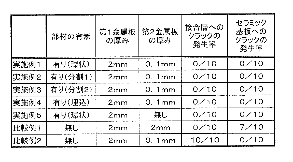
表1から、実施例1~5に係る評価サンプルは、いずれも接合層24及びセラミック基板12にクラックが発生しなかった。これは、第1金属板14の表面14aに部材18を接合したことから、第1金属板14とセラミック基板12との界面32aに発生する熱応力が緩和されたことによるものと考えられる。
これに対して、比較例1は、いずれも接合層24にはクラックが生じていなかったが、10個の評価サンプル中、7個の評価サンプルにおいてセラミック基板102にクラックが発生していた。比較例2は、いずれもセラミック基板102にはクラックが生じていなかったが、10個の評価サンプル全てにおいて接合層24にクラックが発生していた。
[第2実施例]
実施例6~12について、接合層24及びセラミック基板12へのクラックの有無を評価した。評価結果を後述する表2に示す。
実施例6~12について、接合層24及びセラミック基板12へのクラックの有無を評価した。評価結果を後述する表2に示す。
セラミック基板12のために、曲げ強度が650MPaで、厚みが0.3mmの窒化珪素(Si3N4)基板を用意した。Si3N4基板は、熱膨張係数が3.1ppm/K、ヤング率が330GPaである。第1金属板14及び第2金属板16のために、無酸素Cu板を用意した。無酸素Cu板は、熱膨張係数が16.5ppm/K、ヤング率が129.8GPaである。また、Ti活性金属粉末を添加したAg-Cu系のろう材ペーストを用意した。
(実施例6)
部材18のために、厚みが0.3mmのアルミナ(Al2O3)基板を用意した。Al2O3基板は、熱膨張係数が7.2ppm/K、ヤング率が310GPaである。そして、実施例6に係る評価サンプルのセラミック回路基板は、上述した第1実施例と同様に、図11A及び図11Bに示す第2セラミック回路基板10Bと同様の構成を有する。すなわち、環状の部材18を使用した(表2において「(環状配置)」と表記した)。
部材18のために、厚みが0.3mmのアルミナ(Al2O3)基板を用意した。Al2O3基板は、熱膨張係数が7.2ppm/K、ヤング率が310GPaである。そして、実施例6に係る評価サンプルのセラミック回路基板は、上述した第1実施例と同様に、図11A及び図11Bに示す第2セラミック回路基板10Bと同様の構成を有する。すなわち、環状の部材18を使用した(表2において「(環状配置)」と表記した)。
先ず、セラミック基板12及び部材18にろう材を厚み10μm塗布し、Cu板(第1金属板14及び第2金属板16)を接合した。第1金属板14の厚みt1は2mm、第2金属板16の厚みt2は0.1mmとした。接合条件は、真空下、温度800℃、1MPaで加熱加圧接合した。その後、図17A及び図17Bに示すように、パワー半導体26を接合層24(この場合、半田層)で接合し、実施例6に係る評価サンプルとした。10個の評価サンプルを作製した。
(実施例7)
部材18のために、厚みが0.3mmのアルミナ-ジルコニア(Al2O3-ZrO2)基板を用意したこと以外は、上述した実施例6と同様にして、実施例7に係る10個の評価サンプルを作製した。Al2O3-ZrO2基板は、Al2O3を80質量%、ZrO2を20質量%含有する。また、熱膨張係数が8.3ppm/K、ヤング率が380GPaである。
部材18のために、厚みが0.3mmのアルミナ-ジルコニア(Al2O3-ZrO2)基板を用意したこと以外は、上述した実施例6と同様にして、実施例7に係る10個の評価サンプルを作製した。Al2O3-ZrO2基板は、Al2O3を80質量%、ZrO2を20質量%含有する。また、熱膨張係数が8.3ppm/K、ヤング率が380GPaである。
(実施例8)
部材18のために、厚みが0.3mmの炭化珪素(SiC)基板を用意したこと以外は、上述した実施例6と同様にして、実施例8に係る10個の評価サンプルを作製した。SiC基板は、熱膨張係数が3.8ppm/K、ヤング率が390GPaである。
部材18のために、厚みが0.3mmの炭化珪素(SiC)基板を用意したこと以外は、上述した実施例6と同様にして、実施例8に係る10個の評価サンプルを作製した。SiC基板は、熱膨張係数が3.8ppm/K、ヤング率が390GPaである。
(実施例9)
部材18のために、厚みが0.3mmのジルコニア(ZrO2)基板を用意したこと以外は、上述した実施例6と同様にして、実施例9に係る10個の評価サンプルを作製した。ZrO2基板は、熱膨張係数が10.5ppm/K、ヤング率が200GPaである。
部材18のために、厚みが0.3mmのジルコニア(ZrO2)基板を用意したこと以外は、上述した実施例6と同様にして、実施例9に係る10個の評価サンプルを作製した。ZrO2基板は、熱膨張係数が10.5ppm/K、ヤング率が200GPaである。
(実施例10)
部材18のために、厚みが0.3mmのシリコン(Si)基板を用意したこと以外は、上述した実施例6と同様にして、実施例10に係る10個の評価サンプルを作製した。Si基板は、熱膨張係数が3.9ppm/K、ヤング率が190GPaである。
部材18のために、厚みが0.3mmのシリコン(Si)基板を用意したこと以外は、上述した実施例6と同様にして、実施例10に係る10個の評価サンプルを作製した。Si基板は、熱膨張係数が3.9ppm/K、ヤング率が190GPaである。
(実施例11)
部材18のために、厚みが0.3mmのタングステン(W)基板を用意したこと以外は、上述した実施例6と同様にして、実施例11に係る10個の評価サンプルを作製した。W基板は、熱膨張係数が4.3ppm/K、ヤング率が345GPaである。
部材18のために、厚みが0.3mmのタングステン(W)基板を用意したこと以外は、上述した実施例6と同様にして、実施例11に係る10個の評価サンプルを作製した。W基板は、熱膨張係数が4.3ppm/K、ヤング率が345GPaである。
(実施例12)
部材18のために、厚みが0.3mmのタングステン-銅(W-Cu)基板を用意したこと以外は、上述した実施例6と同様にして、実施例12に係る10個の評価サンプルを作製した。W-Cu基板は、Wを80質量%、Cuを20質量%含有する。また、熱膨張係数が8.3ppm/K、ヤング率が290GPaである。
部材18のために、厚みが0.3mmのタングステン-銅(W-Cu)基板を用意したこと以外は、上述した実施例6と同様にして、実施例12に係る10個の評価サンプルを作製した。W-Cu基板は、Wを80質量%、Cuを20質量%含有する。また、熱膨張係数が8.3ppm/K、ヤング率が290GPaである。
<評価>
上述した第1実施例と同様に、評価方法として、温度=-40℃~125℃の熱サイクル試験を実施した。サイクル数=100サイクルとし、1サイクル当たり、-40℃(低温)下で30分、125℃(高温)下で30分保持した。熱サイクル試験終了後に、接合層24へのクラックの発生率と、セラミック基板へのクラックの発生率を評価した。評価結果を下記表2に示す。表2においても、表1と同様に、クラックが発生した評価サンプルの個数/評価サンプルの母数(=10)で表記した。
上述した第1実施例と同様に、評価方法として、温度=-40℃~125℃の熱サイクル試験を実施した。サイクル数=100サイクルとし、1サイクル当たり、-40℃(低温)下で30分、125℃(高温)下で30分保持した。熱サイクル試験終了後に、接合層24へのクラックの発生率と、セラミック基板へのクラックの発生率を評価した。評価結果を下記表2に示す。表2においても、表1と同様に、クラックが発生した評価サンプルの個数/評価サンプルの母数(=10)で表記した。
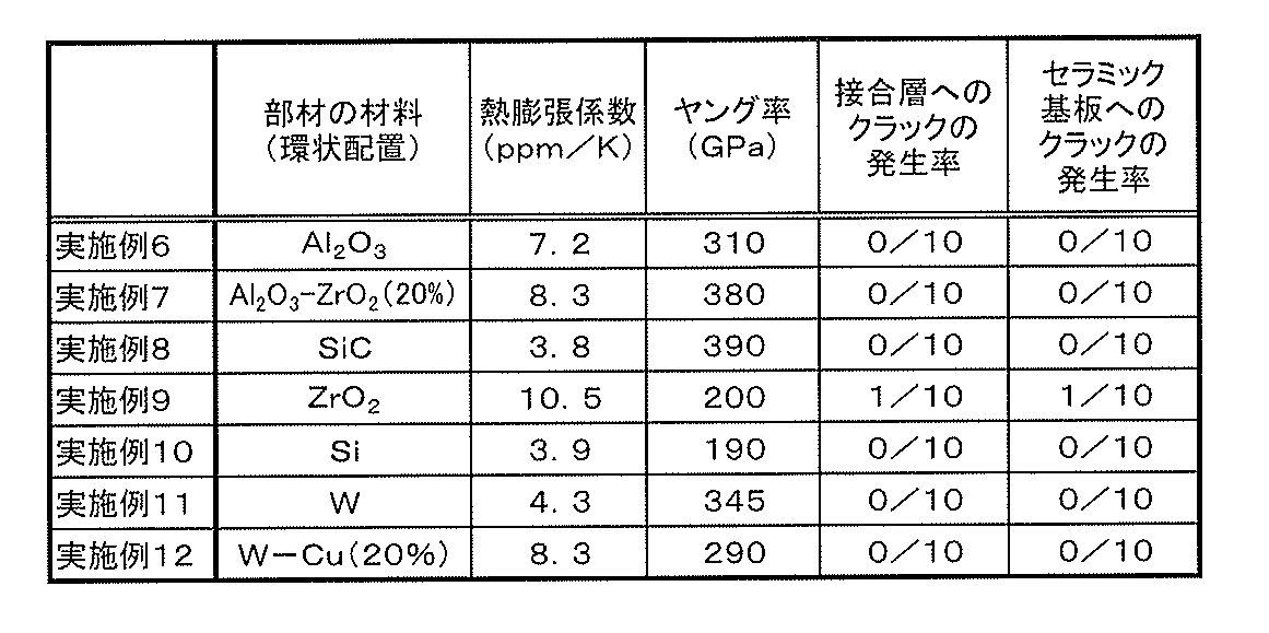
表2から、実施例6~12のうち、実施例9を除く実施例はいずれも接合層24及びセラミック基板12にクラックが発生しなかった。これは、第1金属板14の表面14aに部材18を接合したことから、第1金属板14とセラミック基板12との界面32aに発生する熱応力が緩和されたことによるものと考えられる。
実施例9については、10個の評価サンプル中、1個の評価サンプルにおいて接合層24及びセラミック基板12にクラックが発生していたが、実用上は問題ないレベルである。実施例9のみにクラックが発生したのは、実施例6~12のうち実施例9のZrO2板の熱膨張係数が第1金属板14の熱膨張係数(この場合、16.5ppm/K)に最も近いためと考えられる。
なお、本発明に係るセラミック回路基板及び電子デバイスは、上述の実施の形態に限らず、本発明の要旨を逸脱することなく、種々の構成を採り得ることはもちろんである。
Claims (13)
- セラミック基板(12)と、
前記セラミック基板(12)の表面(12a)に接合された金属板(14)と、
前記金属板(14)の表面(14a)側に接合された部材(18)と、を有し、
前記部材(18)は、前記金属板(14)よりも熱膨張係数が小さく、且つ、ヤング率が大きい材料からなることを特徴とするセラミック回路基板。 - 請求項1記載のセラミック回路基板において、
前記部材(18)は、前記金属板(14)の表面(14a)の外周に沿って環状に形成されていることを特徴とするセラミック回路基板。 - 請求項1記載のセラミック回路基板において、
複数の前記部材(18)が前記金属板(14)の表面(14a)の外周に沿って配列されていることを特徴とするセラミック回路基板。 - 請求項1記載のセラミック回路基板において、
2つの前記部材(18)が線対称の位置に接合されていることを特徴とするセラミック回路基板。 - 請求項1~4のいずれか1項に記載のセラミック回路基板において、
前記部材(18)は、その一部が、前記金属板(14)の表面(14a)の外周よりも横方向に張り出していることを特徴とするセラミック回路基板。 - 請求項1~4のいずれか1項に記載のセラミック回路基板において
前記部材(18)は、その全体が、前記金属板(14)の表面(14a)内に接合されていることを特徴とするセラミック回路基板。 - 請求項1~6のいずれか1項に記載のセラミック回路基板において、
前記金属板(14)の表面(14a)の一部に窪み(20)を有し、
前記部材(18)は、前記窪み(20)に接合されていることを特徴とするセラミック回路基板。 - 請求項1~7のいずれか1項に記載のセラミック回路基板において、
前記部材(18)と前記セラミック基板(12)として、当該セラミック回路基板に反りが発生するのを抑制するように、少なくとも物性及び厚みが調整されたものが用いられていることを特徴とするセラミック回路基板。 - 請求項1~8のいずれか1項に記載のセラミック回路基板において、
前記部材(18)の構成材料は、前記セラミック基板(12)と同様のセラミック材料であることを特徴とするセラミック回路基板。 - 請求項1~9のいずれか1項に記載のセラミック回路基板において、
前記セラミック基板(12)の構成材料は窒化珪素であることを特徴とするセラミック回路基板。 - 請求項1~10のいずれか1項に記載のセラミック回路基板において、
前記セラミック基板(12)の裏面(12b)に別の金属板(16)が接合され、
前記金属板(14)の厚みは前記別の金属板(16)の厚みよりも大きいことを特徴とするセラミック回路基板。 - 請求項11記載のセラミック回路基板において、
前記セラミック基板(12)の厚みをta、前記金属板(14)の厚みをt1、前記別の金属板(16)の厚みをt2としたとき、
t2<ta<t1
であることを特徴とするセラミック回路基板。 - 請求項1~12のいずれか1項に記載のセラミック回路基板と、
前記セラミック回路基板の前記金属板(14)の表面(14a)に実装されたパワー半導体(26)と、を有することを特徴とする電子デバイス。
Priority Applications (2)
| Application Number | Priority Date | Filing Date | Title |
|---|---|---|---|
| JP2015531837A JP6560121B2 (ja) | 2013-08-16 | 2014-08-15 | セラミック回路基板及び電子デバイス |
| US15/040,405 US10147663B2 (en) | 2013-08-16 | 2016-02-10 | Ceramic circuit board and electronic device |
Applications Claiming Priority (2)
| Application Number | Priority Date | Filing Date | Title |
|---|---|---|---|
| JP2013169260 | 2013-08-16 | ||
| JP2013-169260 | 2013-08-16 |
Related Child Applications (1)
| Application Number | Title | Priority Date | Filing Date |
|---|---|---|---|
| US15/040,405 Continuation US10147663B2 (en) | 2013-08-16 | 2016-02-10 | Ceramic circuit board and electronic device |
Publications (1)
| Publication Number | Publication Date |
|---|---|
| WO2015022993A1 true WO2015022993A1 (ja) | 2015-02-19 |
Family
ID=50280299
Family Applications (1)
| Application Number | Title | Priority Date | Filing Date |
|---|---|---|---|
| PCT/JP2014/071473 Ceased WO2015022993A1 (ja) | 2013-08-16 | 2014-08-15 | セラミック回路基板及び電子デバイス |
Country Status (4)
| Country | Link |
|---|---|
| US (1) | US10147663B2 (ja) |
| EP (1) | EP2838325B1 (ja) |
| JP (1) | JP6560121B2 (ja) |
| WO (1) | WO2015022993A1 (ja) |
Cited By (1)
| Publication number | Priority date | Publication date | Assignee | Title |
|---|---|---|---|---|
| JP2018074147A (ja) * | 2016-10-24 | 2018-05-10 | 京セラ株式会社 | 回路基板および電子装置 |
Families Citing this family (9)
| Publication number | Priority date | Publication date | Assignee | Title |
|---|---|---|---|---|
| JP6896734B2 (ja) * | 2016-07-28 | 2021-06-30 | 株式会社東芝 | 回路基板および半導体モジュール |
| WO2018155014A1 (ja) * | 2017-02-23 | 2018-08-30 | 日本碍子株式会社 | 絶縁放熱基板 |
| CN110226363B (zh) * | 2017-03-30 | 2022-08-02 | 株式会社东芝 | 陶瓷铜电路基板及使用了其的半导体装置 |
| EP4539118A1 (en) * | 2023-05-22 | 2025-04-16 | LX Semicon Co., Ltd. | A manufacturing method of a heat dissipation substrate for a power semiconductor module, and a manufacturing method of a power semiconductor module including the same |
| KR20250051279A (ko) * | 2023-10-10 | 2025-04-17 | 주식회사 엘엑스세미콘 | 전력반도체 모듈용 방열 기판의 제조방법 및 이를 이용한 전력반도체 모듈의 제조방법 |
| EP4539116A1 (en) * | 2023-05-22 | 2025-04-16 | LX Semicon Co., Ltd. | A heat dissipation substrate for a power semiconductor module, a power semiconductor module including the heat dissipation substrate, and a power converter including the power semiconductor module |
| EP4539117A1 (en) * | 2023-05-22 | 2025-04-16 | LX Semicon Co., Ltd. | A heat dissipation substrate for a power semiconductor module, a power semiconductor module including the heat dissipation substrate, and a power converter including the power semiconductor module |
| EP4538252A1 (en) * | 2023-05-22 | 2025-04-16 | LX Semicon Co., Ltd. | A manufacturing method of a heat dissipation substrate for a power semiconductor module and a manufacturing method of a power semiconductor module including the same |
| EP4723172A1 (de) * | 2024-10-04 | 2026-04-08 | Siemens Aktiengesellschaft | Anordnung für eine elektronische recheneinheit, verfahren und leistungsmodul |
Citations (8)
| Publication number | Priority date | Publication date | Assignee | Title |
|---|---|---|---|---|
| JP2004327732A (ja) * | 2003-04-24 | 2004-11-18 | Kyocera Corp | セラミック回路基板及び電気回路モジュール |
| JP2006041256A (ja) * | 2004-07-28 | 2006-02-09 | Nissan Motor Co Ltd | 半導体装置及びその製造方法 |
| JP2006294890A (ja) * | 2005-04-12 | 2006-10-26 | Nissan Motor Co Ltd | 半導体装置及びその製造方法 |
| JP2007095942A (ja) * | 2005-09-28 | 2007-04-12 | Nissan Motor Co Ltd | 接合構造 |
| JP2009117701A (ja) * | 2007-11-08 | 2009-05-28 | Toyota Motor Corp | パワーモジュール |
| JP2011222669A (ja) * | 2010-04-07 | 2011-11-04 | Mitsubishi Materials Corp | パワーモジュール用基板及びパワーモジュール |
| JP2012074591A (ja) * | 2010-09-29 | 2012-04-12 | Kyocera Corp | 回路基板および電子装置 |
| JP2014053441A (ja) * | 2012-09-07 | 2014-03-20 | Mitsubishi Electric Corp | 半導体装置 |
Family Cites Families (11)
| Publication number | Priority date | Publication date | Assignee | Title |
|---|---|---|---|---|
| EP0766307B1 (en) * | 1995-03-20 | 2007-08-08 | Kabushiki Kaisha Toshiba | Silicon nitride circuit board |
| JP3671457B2 (ja) * | 1995-06-07 | 2005-07-13 | 株式会社デンソー | 多層基板 |
| EP0874399A1 (en) * | 1996-08-20 | 1998-10-28 | Kabushiki Kaisha Toshiba | Silicon nitride circuit board and semiconductor module |
| US6033787A (en) * | 1996-08-22 | 2000-03-07 | Mitsubishi Materials Corporation | Ceramic circuit board with heat sink |
| JP3847954B2 (ja) | 1998-05-22 | 2006-11-22 | 株式会社東芝 | セラミックス回路基板の製造方法 |
| JP2003086747A (ja) * | 2001-09-10 | 2003-03-20 | Hitachi Ltd | 絶縁回路基板とその製法およびそれを用いた半導体パワー素子 |
| JP2004128510A (ja) * | 2002-10-05 | 2004-04-22 | Semikron Elektron Gmbh | 向上された絶縁強度を有するパワー半導体モジュール |
| JP4565249B2 (ja) * | 2004-08-26 | 2010-10-20 | Dowaメタルテック株式会社 | 金属−セラミックス接合基板およびその製造方法 |
| DE102009033029A1 (de) * | 2009-07-02 | 2011-01-05 | Electrovac Ag | Elektronische Vorrichtung |
| EP2743978B1 (en) * | 2011-08-12 | 2018-05-02 | Mitsubishi Materials Corporation | Substrate for power module, substrate for power module with heat sink, power module, and method for manufacturing substrate for power module |
| DE102012113014A1 (de) * | 2012-12-21 | 2014-06-26 | Epcos Ag | Bauelementträger und Bauelementträgeranordnung |
-
2014
- 2014-03-18 EP EP14160452.0A patent/EP2838325B1/en active Active
- 2014-08-15 WO PCT/JP2014/071473 patent/WO2015022993A1/ja not_active Ceased
- 2014-08-15 JP JP2015531837A patent/JP6560121B2/ja not_active Expired - Fee Related
-
2016
- 2016-02-10 US US15/040,405 patent/US10147663B2/en not_active Expired - Fee Related
Patent Citations (8)
| Publication number | Priority date | Publication date | Assignee | Title |
|---|---|---|---|---|
| JP2004327732A (ja) * | 2003-04-24 | 2004-11-18 | Kyocera Corp | セラミック回路基板及び電気回路モジュール |
| JP2006041256A (ja) * | 2004-07-28 | 2006-02-09 | Nissan Motor Co Ltd | 半導体装置及びその製造方法 |
| JP2006294890A (ja) * | 2005-04-12 | 2006-10-26 | Nissan Motor Co Ltd | 半導体装置及びその製造方法 |
| JP2007095942A (ja) * | 2005-09-28 | 2007-04-12 | Nissan Motor Co Ltd | 接合構造 |
| JP2009117701A (ja) * | 2007-11-08 | 2009-05-28 | Toyota Motor Corp | パワーモジュール |
| JP2011222669A (ja) * | 2010-04-07 | 2011-11-04 | Mitsubishi Materials Corp | パワーモジュール用基板及びパワーモジュール |
| JP2012074591A (ja) * | 2010-09-29 | 2012-04-12 | Kyocera Corp | 回路基板および電子装置 |
| JP2014053441A (ja) * | 2012-09-07 | 2014-03-20 | Mitsubishi Electric Corp | 半導体装置 |
Cited By (1)
| Publication number | Priority date | Publication date | Assignee | Title |
|---|---|---|---|---|
| JP2018074147A (ja) * | 2016-10-24 | 2018-05-10 | 京セラ株式会社 | 回路基板および電子装置 |
Also Published As
| Publication number | Publication date |
|---|---|
| JP6560121B2 (ja) | 2019-08-14 |
| US10147663B2 (en) | 2018-12-04 |
| JPWO2015022993A1 (ja) | 2017-03-02 |
| US20160163617A1 (en) | 2016-06-09 |
| EP2838325B1 (en) | 2021-06-16 |
| EP2838325A1 (en) | 2015-02-18 |
Similar Documents
| Publication | Publication Date | Title |
|---|---|---|
| JP6560121B2 (ja) | セラミック回路基板及び電子デバイス | |
| JP6139329B2 (ja) | セラミック回路基板及び電子デバイス | |
| KR102387210B1 (ko) | 히트 싱크 부착 파워 모듈용 기판 및 파워 모듈 | |
| CN110383467B (zh) | 半导体装置 | |
| US10160690B2 (en) | Silicon nitride circuit board and semiconductor module using the same | |
| WO2018173921A1 (ja) | セラミックス金属回路基板およびそれを用いた半導体装置 | |
| JP2013042165A (ja) | 回路基板及びこれを用いた半導体モジュール、回路基板の製造方法 | |
| JP6276424B2 (ja) | 回路基板および電子装置 | |
| CN110544871B (zh) | 半导体激光器的封装结构及叠阵结构 | |
| US9460984B2 (en) | Heat dissipating circuit board and electronic device | |
| CN109478538B (zh) | 电路基板以及半导体模块 | |
| JP6681660B2 (ja) | ヒートシンク付パワーモジュール用基板及びパワーモジュール | |
| US11955450B2 (en) | Method for producing a semiconductor arrangement | |
| US20250233032A1 (en) | Double-sided cooling semiconductor device | |
| JP2012009787A (ja) | パワーモジュール用基板及びその製造方法 | |
| JP5319463B2 (ja) | 位置決め性を向上した窒化珪素基板、およびそれを用いた半導体装置 | |
| JP7662505B2 (ja) | 放熱基板 | |
| US11289397B2 (en) | Heat sink board for a semiconductor device | |
| JP2008135595A (ja) | パワーモジュール | |
| JP6538524B2 (ja) | 回路基板および電子装置 | |
| KR20140116653A (ko) | 소자 패키지 | |
| JP2007116111A (ja) | セラミックス回路基板の製造方法 | |
| JP2016162836A (ja) | 電子部品搭載用パッケージおよび電子装置ならびに電子モジュール |
Legal Events
| Date | Code | Title | Description |
|---|---|---|---|
| 121 | Ep: the epo has been informed by wipo that ep was designated in this application |
Ref document number: 14836444 Country of ref document: EP Kind code of ref document: A1 |
|
| ENP | Entry into the national phase |
Ref document number: 2015531837 Country of ref document: JP Kind code of ref document: A |
|
| NENP | Non-entry into the national phase |
Ref country code: DE |
|
| 122 | Ep: pct application non-entry in european phase |
Ref document number: 14836444 Country of ref document: EP Kind code of ref document: A1 |