WO2015020106A1 - Ledモジュール及びled照明器具 - Google Patents
Ledモジュール及びled照明器具 Download PDFInfo
- Publication number
- WO2015020106A1 WO2015020106A1 PCT/JP2014/070775 JP2014070775W WO2015020106A1 WO 2015020106 A1 WO2015020106 A1 WO 2015020106A1 JP 2014070775 W JP2014070775 W JP 2014070775W WO 2015020106 A1 WO2015020106 A1 WO 2015020106A1
- Authority
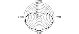
- WO
- WIPO (PCT)
- Prior art keywords
- light emitting
- led module
- emitting diodes
- wiring board
- printed wiring
- Prior art date
- Legal status (The legal status is an assumption and is not a legal conclusion. Google has not performed a legal analysis and makes no representation as to the accuracy of the status listed.)
- Ceased
Links
Images







Classifications
-
- F—MECHANICAL ENGINEERING; LIGHTING; HEATING; WEAPONS; BLASTING
- F21—LIGHTING
- F21V—FUNCTIONAL FEATURES OR DETAILS OF LIGHTING DEVICES OR SYSTEMS THEREOF; STRUCTURAL COMBINATIONS OF LIGHTING DEVICES WITH OTHER ARTICLES, NOT OTHERWISE PROVIDED FOR
- F21V19/00—Fastening of light sources or lamp holders
- F21V19/001—Fastening of light sources or lamp holders the light sources being semiconductors devices, e.g. LEDs
- F21V19/0015—Fastening arrangements intended to retain light sources
- F21V19/002—Fastening arrangements intended to retain light sources the fastening means engaging the encapsulation or the packaging of the semiconductor device
-
- F—MECHANICAL ENGINEERING; LIGHTING; HEATING; WEAPONS; BLASTING
- F21—LIGHTING
- F21K—NON-ELECTRIC LIGHT SOURCES USING LUMINESCENCE; LIGHT SOURCES USING ELECTROCHEMILUMINESCENCE; LIGHT SOURCES USING CHARGES OF COMBUSTIBLE MATERIAL; LIGHT SOURCES USING SEMICONDUCTOR DEVICES AS LIGHT-GENERATING ELEMENTS; LIGHT SOURCES NOT OTHERWISE PROVIDED FOR
- F21K9/00—Light sources using semiconductor devices as light-generating elements, e.g. using light-emitting diodes [LED] or lasers
- F21K9/20—Light sources comprising attachment means
- F21K9/23—Retrofit light sources for lighting devices with a single fitting for each light source, e.g. for substitution of incandescent lamps with bayonet or threaded fittings
- F21K9/232—Retrofit light sources for lighting devices with a single fitting for each light source, e.g. for substitution of incandescent lamps with bayonet or threaded fittings specially adapted for generating an essentially omnidirectional light distribution, e.g. with a glass bulb
-
- F—MECHANICAL ENGINEERING; LIGHTING; HEATING; WEAPONS; BLASTING
- F21—LIGHTING
- F21V—FUNCTIONAL FEATURES OR DETAILS OF LIGHTING DEVICES OR SYSTEMS THEREOF; STRUCTURAL COMBINATIONS OF LIGHTING DEVICES WITH OTHER ARTICLES, NOT OTHERWISE PROVIDED FOR
- F21V29/00—Protecting lighting devices from thermal damage; Cooling or heating arrangements specially adapted for lighting devices or systems
- F21V29/50—Cooling arrangements
- F21V29/70—Cooling arrangements characterised by passive heat-dissipating elements, e.g. heat-sinks
-
- F—MECHANICAL ENGINEERING; LIGHTING; HEATING; WEAPONS; BLASTING
- F21—LIGHTING
- F21Y—INDEXING SCHEME ASSOCIATED WITH SUBCLASSES F21K, F21L, F21S and F21V, RELATING TO THE FORM OR THE KIND OF THE LIGHT SOURCES OR OF THE COLOUR OF THE LIGHT EMITTED
- F21Y2107/00—Light sources with three-dimensionally disposed light-generating elements
- F21Y2107/40—Light sources with three-dimensionally disposed light-generating elements on the sides of polyhedrons, e.g. cubes or pyramids
-
- F—MECHANICAL ENGINEERING; LIGHTING; HEATING; WEAPONS; BLASTING
- F21—LIGHTING
- F21Y—INDEXING SCHEME ASSOCIATED WITH SUBCLASSES F21K, F21L, F21S and F21V, RELATING TO THE FORM OR THE KIND OF THE LIGHT SOURCES OR OF THE COLOUR OF THE LIGHT EMITTED
- F21Y2115/00—Light-generating elements of semiconductor light sources
- F21Y2115/10—Light-emitting diodes [LED]
-
- H—ELECTRICITY
- H10—SEMICONDUCTOR DEVICES; ELECTRIC SOLID-STATE DEVICES NOT OTHERWISE PROVIDED FOR
- H10W—GENERIC PACKAGES, INTERCONNECTIONS, CONNECTORS OR OTHER CONSTRUCTIONAL DETAILS OF DEVICES COVERED BY CLASS H10
- H10W90/00—Package configurations
Definitions
- the present invention relates to an LED module and an LED lighting apparatus.
- LED lighting fixtures using light-emitting diodes with low energy consumption and long life as a light source are becoming popular in place of conventional fluorescent lamps.
- a plurality of light emitting diodes are mounted on a printed wiring board.
- the plurality of light emitting diodes are generally juxtaposed on a printed wiring board as disclosed in, for example, Japanese Patent Application Laid-Open No. 2009-170114.
- a plurality of light emitting diodes are arranged in a plane on a flat printed wiring board, and thus a light source formed by the plurality of light emitting diodes has directivity. That is, in the conventional LED lighting fixture, the luminous intensity of the front surface (normal direction) of the light emitting diode mounting surface is high, but the luminous intensity decreases as the angle with respect to the front surface of the light emitting diode mounting surface increases. Therefore, there is a disadvantage that the brightness is not uniform due to the positional relationship with the LED lighting apparatus.
- an LED lighting apparatus in which a prism is laminated on the light emitting side of the light emitting diode so that the light from the light source is refracted in the lateral direction.
- a prism is laminated on the light emitting side of the light emitting diode so that the light from the light source is refracted in the lateral direction.
- This invention is made
- the present inventors have arranged the light-emitting diode only on the side surface of the straight cone (or frustum), and the inclination angle with respect to the bottom surface of the side surface of this straight cone is 55 ° or more and 82 ° or less.
- an LED module according to an aspect of the present invention made to solve the above-described problem is an LED module including a plurality of light-emitting diodes, and the plurality of light-emitting diodes are a right cone, a right pyramid, a right truncated cone, or a right cone.
- An angle of inclination with respect to the bottom surface of the side surface is 55 ° or more and 82 ° or less, and the light emitting surfaces of the plurality of light emitting diodes are substantially parallel to the side surface,
- an LED lighting apparatus made to solve the above-described problems is an LED lighting apparatus including the LED module.
- the LED module and the LED lighting apparatus of the present invention can effectively suppress fluctuations in the light intensity on the front side at low cost, and can reduce unevenness in brightness on the front side.
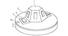
- FIG. 1 is a schematic perspective view showing an LED module according to an embodiment of the present invention.
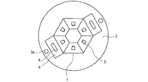
- FIG. 2 is a schematic plan view of the LED module of FIG. 1 viewed from the front surface side of the flexible printed wiring board.
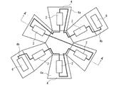
- FIG. 3A is a schematic plan view in which a flexible printed wiring board on which the light emitting diode of FIG. 1 is mounted is developed on a plane.
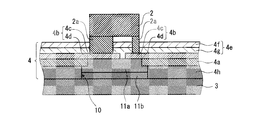
- FIG. 3B is a schematic partial cross-sectional view taken along line AA in FIG. 3A.
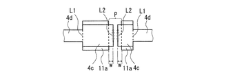
- FIG. 3C is a schematic partial plan view of the flexible printed wiring board of FIG. 3A viewed from the front side.
- 3D is a schematic partial plan view of the flexible printed wiring board of FIG. 3A viewed from the front side.
- FIG. 3A is a schematic perspective view showing an LED module according to an embodiment of the present invention.
- FIG. 2 is a schematic plan view of the LED module of FIG. 1 viewed from the front surface side of the flexible printed wiring board.
- FIG. 3A is a schematic plan view
- FIG. 3E is a schematic partial cross-sectional view showing an LED module according to an embodiment different from FIG. 3B.
- FIG. 3F is a schematic partial cross-sectional view showing an LED module according to an embodiment different from those shown in FIGS. 3B and 3E.
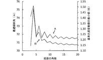
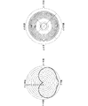
- FIG. 4A is a graph showing a relationship between the number of corners of the bottom surface of the truncated pyramid and the reference light intensity fluctuation value or the optimum inclination angle.
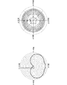
- FIG. 4B is a graph (light distribution curve) showing an example of directivity of the LED module when the bottom surface of the truncated pyramid is a regular pentagon.
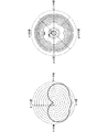
- FIG. 4C is a graph (light distribution curve) showing an example of directivity of the LED module when the bottom surface of the truncated pyramid is a regular hexagon.
- FIG. 4D is a graph (light distribution curve) showing an example of directivity of the LED module when the bottom surface of the truncated pyramid is a regular heptagon.
- FIG. 5 is a graph (light distribution curve) showing the directivity of one light emitting diode.
- FIG. 6 is a schematic front view showing a method of manufacturing the flexible printed wiring board of FIG.
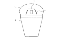
- FIG. 7 is a schematic front view showing an LED lighting apparatus according to an embodiment of the present invention.
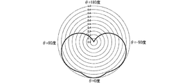
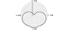
- FIG. 8A is a graph (light distribution curve) showing the directivity of the LED module of an example having an inclination angle of 69 °.
- FIG. 8B is a graph (light distribution curve) showing the directivity of the LED module of the example having an inclination angle of 70 °.
- FIG. 8C is a graph (light distribution curve) showing the directivity of the LED module of the example having an inclination angle of 71 °.
- FIG. 9 is a graph showing the relationship between the tilt angle of the truncated pyramid and the reference light intensity fluctuation value.
- FIG. 10 is a graph showing the relationship between the inclination angle of the truncated pyramid and the ratio of the central luminous intensity to the maximum luminous intensity.
- An LED module according to an aspect of the present invention made to solve the above-described problem is an LED module including a plurality of light-emitting diodes, wherein the plurality of light-emitting diodes are a right cone, a right pyramid, a right truncated cone or a right pyramid.
- the light-emitting surface of the plurality of light-emitting diodes is disposed on only the side surface of the base, has an inclination angle with respect to the bottom surface of the side surface of 55 ° to 82 °, and is substantially parallel to the side surface.
- the angles formed by the projection lines on the bottom surface of the normal line of the light emitting surface of the diode group are all equal and 72 ° or less.
- the LED module includes a plurality of light emitting diodes arranged on a side surface of a right cone (right cone, right angle cone, right truncated cone or right angle frustum) in a three-dimensional manner and spaced within 72 ° in plan view so as to be substantially parallel to the side surface. (So that the polygon connecting the positions of the centers of gravity of the respective light emitting diodes is 5 or more), and the inclination angle of the side surface with respect to the bottom surface is within the above range.
- a right cone right cone, right angle cone, right truncated cone or right angle frustum
- the LED module has a light source (light emitting diode group) in the hemispherical omnidirectional (front side of the LED module) on the apex side centered on the center of the bottom surface of the straight cone on which the plurality of light emitting diodes are arranged.
- the variation in luminous intensity due to the relative position with respect to can be reduced.
- the luminous intensity uniformity in all the hemispherical directions can be remarkably improved. That is, the LED module can effectively suppress fluctuations in luminous intensity on the front side at low cost without providing a member such as a prism.
- the “light-emitting diode group” means a group composed of a plurality of light-emitting diodes having an angle formed by a projection line on the normal cone of the normal surface of the light-emitting surface or the bottom surface of the frustum of frustum within 10 °.
- the “normal line of the light emitting surface of the light emitting diode group” means a normal line of a straight cone or a side surface of the right frustum that passes through the geometric center of gravity of the plurality of light emitting diodes included in the light emitting diode group.
- the inclination angle of the side surface with respect to the bottom is more preferably 60 ° or more and 80 ° or less.
- the side surface on which the plurality of light emitting diodes are disposed is a side surface of a right-angled pyramid or a right-angled frustum, and one or more light-emitting diodes are disposed on this side surface, and the bottom surface of the right-angled pyramid or the right-angled frustum is defined as all inner angles. It is good that it is a polygon with five or more equal angles. Thus, by making the right cone with the light emitting diodes a right-angled pyramid or a right-angled frustum, it is possible to facilitate the arrangement of the light emitting diodes on the side surfaces of the right cone.
- the luminous intensity around the central axis (circumferential direction) of the straight cone of the LED module is made more uniform. Can do.
- the number of corners on the bottom of the right-angled pyramid or right-angled frustum is preferably an odd number.
- the number of corners on the bottom of the right-angled pyramid or the right-angled frustum is an odd number (2n-1, n is a natural number). It has been found that the effect of uniformizing the luminous intensity is higher than in the case of the even number (2n) in which the number of corners on the bottom surface is 1 larger than the odd number.
- the side surface on which the plurality of light emitting diodes are arranged may be a right cone or a side surface of a right truncated cone, and the light emitting diodes or light emitting diode groups may be arranged at equiangular intervals.
- the straight cone is a right cone or a right truncated cone and a plurality of light emitting diodes or light emitting diode groups are arranged at equiangular intervals, the LED module around the central axis (circumferential direction) of the straight cone is provided.
- the luminous intensity can be made more uniform.
- a metal substrate having a convex part of the right cone, right pyramid, right frustum or right frustum shape at the center is further provided, and the plurality of light emitting diodes are mounted on a flexible printed wiring board. It is good to arrange
- the convex portion of the metal base material may be formed by die casting, cold forging, cutting, or press molding. By forming the convex portions in this manner, the LED module can be manufactured more easily, and thus the manufacturing cost of the LED module can be further reduced.
- the LED module may further include a heat sink on the back side of the metal base.
- a heat sink on the back side of the metal base, heat generation of the light emitting diode can be more effectively suppressed, and the life of the LED module can be extended.
- the flexible printed wiring board is laminated on the surface of the base film, a conductive pattern that is laminated on the surface side of the base film, and includes one or a plurality of land portions and a wiring portion that is connected to the land portion.
- a cover lay having an opening formed at a position corresponding to the one or more land portions, and one or more land portions on which the light emitting diode is mounted on the back surface of the flexible printed wiring board. It is preferable to further include a heat conductive adhesive that has a recess reaching the back surface of the conductive pattern in at least a part of the projection area and is filled in the recess.
- the conductive pattern and the metal substrate are connected via the thermal conductive adhesive, so the heat dissipation effect of the light-emitting diode is significantly accelerated. can do.
- the “land portion” refers to a portion in which the wiring is expanded to a size capable of solder connection in order to perform solder connection for mounting a chip component in the middle of the wiring circuit in the conductive pattern.
- an opening is formed at a position corresponding to this portion of the cover lay to expose the conductive portion for solder connection.
- the opening is relatively small with respect to the size of the land, the entire surface of the opening becomes a circuit surface (conductive portion).
- a pad-shaped circuit surface corresponding to the land portion and a wiring portion connected thereto may exist in the opening.
- the base film may be left in a region including at least a part of the periphery of the one or more land portions in a plan view substantially perpendicular to the surface of the flexible printed wiring board.
- the conductive pattern is applied to the metal substrate when the flexible printed wiring board on which the light emitting diode is mounted is attached to the metal substrate.
- production of the short circuit by contact can be prevented.
- substantially perpendicular means that the angle formed with the plane is within 90 ⁇ 5 °.
- the recess is formed in an area that covers at least the projection area of the opening of the coverlay.
- the heat dissipation effect of the light emitting diode can be further promoted.
- the concave portion is formed in a region covering at least the projection region of the light emitting diode, and a coverlay exists between the plurality of land portions in a plan view substantially perpendicular to the surface of the flexible printed wiring board.
- a coverlay exists between the plurality of land portions in a plan view substantially perpendicular to the surface of the flexible printed wiring board.
- the flexible printed wiring board has a through-hole for each projection region of the one or more land portions, and the thermally conductive adhesive is also filled in the through-hole and the upper portion thereof, and is in contact with the back surface of the light emitting diode. It is good to be.
- the through hole in the flexible printed wiring board in this way, it is possible to prevent the heat conductive adhesive from leaking out of the projection area of the land portion when the heat conductive adhesive is filled.
- the heat dissipation effect of a light emitting diode can further be accelerated
- the LED module in the range of ⁇ 90 ° to 90 ° to the left and right from this reference direction
- the variation in luminous intensity is preferably 2.5 or less.
- An LED lighting apparatus made to solve the above problems is an LED lighting apparatus including the LED module.
- the LED lighting apparatus includes the LED module, it is possible to prevent uneven brightness due to the relative position with the light source at low cost.
- the LED lighting apparatus can be suitably used as a light bulb.
- Luminosity is a value measured according to JIS-C7801 (2009).
- front and back in the embodiment of the LED module means a direction in which the light emitting diode lamination side is the front and the opposite side to the light emitting diode lamination side is the back in the thickness direction of the base film of the flexible printed wiring board, It does not mean the front and back of the LED module in use.
- LED module First, an embodiment of an LED module according to the present invention will be described.
- the LED module shown in FIGS. 1 and 2 mainly includes a plurality of light emitting diodes 2 disposed on the side surface of the right-angle frustum portion 1.
- the LED module includes a plurality of light emitting diodes 2, a metal base 3 having a convex portion having substantially the same shape as the right-angle frustum portion 1, and a convex portion on the surface side of the metal base 3.
- stacked on the back surface side of the said metal base material 3 are provided.
- the right-angle frustum part 1 is comprised by the part laminated
- a surface having a large area is on the metal substrate 3 side, and a bottom surface and an upper surface (a surface facing the bottom surface) are substantially parallel to the surface of the metal substrate 3.
- the plurality of light emitting diodes 2 are disposed in a region forming the side surface of the right-angle frustum portion 1 on the surface of the flexible printed wiring board 4.
- the metal substrate 3 is a metal bulk or plate member, and has a convex portion at the center.
- This convex part is substantially the same shape as the right-angle frustum part 1, and the right-angle frustum part 1 is formed by laminating
- metal forming the metal substrate 3 for example, aluminum, magnesium, copper, iron, nickel, molybdenum, tungsten, or the like can be used. Among these, aluminum excellent in heat conductivity, workability and lightness is particularly preferable.
- the upper limit of the average thickness of the metal substrate 3 is preferably 4 mm, and more preferably 3 mm.
- the average thickness of the metal substrate 3 is less than the above lower limit, the strength of the metal substrate 3 may be insufficient.
- the average thickness of the metal substrate 3 exceeds the above upper limit, it may be difficult to form convex portions by press molding or the like, and the weight and volume of the LED module may become unnecessarily large. is there.
- the shape of the metal base 3 in plan view can be appropriately designed according to the shape of the lighting fixture using the LED module, and can be a polygonal shape in addition to the circular shape shown in FIGS.
- the diameter can be, for example, 10 mm or more and 200 mm or less.
- the method for forming the convex portion of the metal base 3 is not particularly limited, but can be easily and reliably formed by die casting, cold forging, cutting, or press molding.
- the metal substrate 3 having a convex portion can be formed by pressing a mold having a convex portion shape against a metal flat plate.
- the metal base 3 has a through hole 3a through which a lead wire for connecting a power supply circuit for supplying power to the LED module and the conductive pattern 4b of the flexible printed wiring board 4 is inserted.
- a lead wire for connecting a power supply circuit for supplying power to the LED module and the conductive pattern 4b of the flexible printed wiring board 4 is inserted.
- two through holes 3a are provided one by one at positions facing each other across the right-angle frustum portion 1, but the formation position of the through holes 3a is not limited to this,
- the through hole 3a may be formed at a position where connection between a connector 6 and a lead wire, which will be described later, becomes easy.
- the flexible printed wiring board 4 includes a base film 4a having flexibility and insulation, a conductive pattern 4b laminated on the surface side of the base film 4a, and a base film 4a and a conductive pattern 4b. And a coverlay 4e laminated on the surface of the main body.
- the conductive pattern 4b has a plurality of land portions 4c and a wiring portion 4d connected to the land portions 4c, and the light emitting diode 2 is electrically connected to the land portions 4c via solder 2a. It is arranged (mounted) as follows.
- the cover lay 4e is formed with openings at positions corresponding to the plurality of land portions 4c.
- FIG. 3A shows a flat development view before the flexible printed wiring board 4 is laminated along the convex portion of the metal base 3. For ease of viewing, the coverlay 4e is omitted in FIG. 3A.
- the base film 4a which comprises the said flexible printed wiring board 4 is comprised by the sheet-like member which has insulation and flexibility.
- a resin film can be used as the sheet-like member constituting the base film 4a.
- the main component of this resin film for example, polyimide, polyethylene terephthalate or the like is preferably used.
- the base film 4a may include a filler, an additive, and the like.
- “main component” means a component contained in an amount of 50% by mass or more.
- the base film 4a has a planar shape in which a plurality of trapezoids of the same shape are joined so that each side of the regular polygon and the upper side are shared, and only in the plurality of trapezoidal portions.
- a light emitting diode 2 is mounted.
- the base film 4a is bent at the connection side between the regular polygon and each trapezoid so as to follow the convex portion of the metal base 3, and the regular polygon portion is laminated on the upper surface of the convex portion of the metal base 3.
- Each trapezoidal part is laminated on the side surface of.
- a rectangular region is further connected to the lower sides of the two trapezoidal portions facing each other on the base film 4a, and a connector 6 described later is mounted on the rectangular portion.
- the base film 4 a is laminated on the metal base 3
- the base film 4 a is also bent at the connection side between the trapezoid and the rectangle, and the rectangular portion is laminated on the flat surface around the convex portion of the metal base 3.
- the portion for mounting the connector 6 is not limited to the rectangular shape and position shown in FIGS. 1 to 3A, but can be formed in any shape and position, and can be omitted when the connector 6 is mounted on the trapezoidal portion. It is.
- the base film 4a preferably has a shape such that the hypotenuses of adjacent trapezoidal portions come into contact with each other when arranged along the convex portion of the metal base 3.
- the base film 4a by making the base film 4a into a shape in which the hypotenuses of the trapezoidal portions come into contact with each other, it is possible to prevent the surface of the metal base 3 from appearing in the right-angled frustum portion 1, and to adjust the luminous intensity of the LED module. Uniformity and design can be improved.
- the lower limit of the average thickness of the base film 4a is preferably 9 ⁇ m, and more preferably 12 ⁇ m.
- the upper limit of the average thickness of the base film 4a is preferably 50 ⁇ m, and more preferably 38 ⁇ m.
- the strength of the base film 4a may be insufficient.
- the average thickness of the base film 4a exceeds the above upper limit, it may be difficult to bend the base film 4a into a straight cone shape along the convex portion.
- the conductive pattern 4b has a plurality of land portions 4c and wiring portions 4d connected to the land portions 4c, and a desired planar shape (pattern) is obtained by etching a metal layer laminated on the surface of the base film 4a. Is formed.
- One land portion 4c is provided in each trapezoidal portion of the base film 4a, and the light emitting diode 2 is mounted on each land portion 4c.
- the wiring part 4d is formed so as to connect the plurality of land parts 4c and the connector 6 in series.
- the conductive pattern 4b can be formed of a conductive material, but is generally formed of copper, for example.
- the lower limit of the average thickness of the conductive pattern 4b is preferably 5 ⁇ m, and more preferably 8 ⁇ m.
- the upper limit of the average thickness of the conductive pattern 4b is preferably 75 ⁇ m, and more preferably 50 ⁇ m.
- the conductivity may be insufficient.
- the average thickness of the conductive pattern 4b exceeds the above upper limit, the flexibility of the flexible printed wiring board 4 may be impaired.
- the flexible printed wiring board 4 further includes an adhesive layer 4h laminated on the back surface of the base film 4a, and is adhered to the metal substrate 3 by the adhesive layer 4h.
- the adhesive layer 4 h is a layer mainly composed of an adhesive capable of bonding the base film 4 a to the metal base 3.
- the adhesive is not particularly limited, and for example, a thermosetting adhesive such as an epoxy adhesive, a silicone adhesive, and an acrylic adhesive can be used.
- the adhesive layer 4h can contain an additive as necessary. However, since the LED module includes thermal conductive adhesive layers 11a and 11b described later, it is not necessary to impart thermal conductivity to the adhesive layer 4h.
- the lower limit of the average thickness of the adhesive layer 4h is preferably 5 ⁇ m and more preferably 10 ⁇ m.
- the upper limit of the average thickness of the adhesive layer 4h is preferably 50 ⁇ m, and more preferably 25 ⁇ m.
- the LED module may become unnecessarily thick, or the distance between the conductive pattern 4b and the metal substrate 3 will increase, resulting in poor heat dissipation. May be sufficient.
- an opening is formed that defines the back side portion of the concave portion 10 filled with heat conductive adhesive layers 11a and 11b described later.
- the size of the opening of the back side portion, that is, the back side portion of the concave portion 10 in the adhesive layer 4 h is larger than the size of the opening of the front side portion of the concave portion 10, that is, the concave portion 10 in the base film 4 a described later.
- the filling operation of the heat conductive adhesive layers 11a and 11b can be facilitated by increasing the opening of the concave portion 10 in the adhesive layer 4h.
- the adhesive layer 4h having an opening for defining the back side portion of the concave portion 10 is formed after the base film 4a is removed and the front side portion of the concave portion 10 is formed, these positions are easily aligned.
- the LED module has a recess 10 that reaches the back surface of the conductive pattern 4b in at least a part of the projected area of the plurality of land portions 4c on which the one light emitting diode 2 is mounted, of the back surface of the flexible printed wiring board 4. Further, as shown in FIG. 3C, a peripheral edge L2 facing the connection edge L1 of the plurality of land portions 4c with the wiring portion 4d in a plan view substantially perpendicular to the surface of the flexible printed wiring board 4 in the concave portion 10.
- the base film 4a remains in the remaining region P including This remaining area P is also an area between the pair of land portions 4c.
- connection edge with the wiring part means the boundary line between the wiring part and the land part
- the “periphery opposite to the connection edge with the wiring part” means the connection edge among the peripheral edges of the land part. It means a portion where an imaginary straight line passing through the upper point and the geometric center of gravity of the land portion intersects.
- the concave portion 10 is formed in a region overlapping with the projection region of the light emitting diode 2 mounted on the land portion 4c located on the bottom surface thereof. That is, the front side portion of the concave portion 10 is formed by removing the base film 4 a in a region covering the projection region of the light emitting diode 2 except for the remaining region P. Moreover, the back side part of the recessed part 10 is formed in the area
- the projected areas of the plurality of land portions 4c all overlap with the opening area (including the front side portion and the remaining area P) of the recess 10 in the base film 4a in plan view.
- a part of the projected area of the land portion 4c may not overlap the opening area of the recess 10 in the base film 4a.
- the lower limit of the ratio of the overlapping area (excluding the remaining region P) of the concave portion 10 and the land portion 4c in the base film 4a to the total area of the land portion 4c is preferably 80%, more preferably 90%, and 95%. Further preferred. When the said area ratio is less than the said minimum, there exists a possibility that the heat transfer effect of the said LED module may become inadequate.
- the front side portion of the recess 10 is formed in a region that covers at least the projection region of the opening of the cover lay 4e provided at a position corresponding to the plurality of land portions 4c. Yes. Further, at least the front side portion of the recess 10 is formed in a region covering at least the projection region of the light emitting diode 2, and a cover layout is provided between the plurality of land portions 4 c in a plan view substantially perpendicular to the surface of the flexible printed wiring board 4. 4e exists. 3B, the projection area of the opening H of the cover lay 4e of the flexible printed wiring board 4 is smaller than the projection area of the land portion 4c as shown in FIG. 3D, and exists within the projection area of the land portion 4c. That is, a part of the land portion 4 c is exposed by the opening H.
- the upper limit of the opening area of the recess 10 in the base film 4a is preferably twice the projected area of the light emitting diode 2, more preferably 1.8 times, and even more preferably 1.5 times.
- the “opening area of the recess” means the area of the bottom surface of the recess (the conductive pattern or the exposed back surface of the coverlay) and does not include the area of the remaining region P.
- the lower limit of the difference between the opening diameter of the recess 10 in the base film 4a (the diameter of the front portion) and the opening diameter of the recess 10 in the adhesive layer 4h (the diameter of the back portion) is preferably 2 ⁇ m, more preferably 40 ⁇ m, and 100 ⁇ m. Is more preferable.
- the upper limit of the difference between the opening diameter of the recess 10 in the base film 4a and the opening diameter of the recess 10 in the adhesive layer 4h is preferably 1000 ⁇ m, more preferably 600 ⁇ m, and even more preferably 200 ⁇ m.
- the filling work of the heat conductive adhesive layers 11a and 11b is insufficiently facilitated. There is a risk.
- the filling amount of the heat conductive adhesive layers 11a and 11b increases, There is a possibility that the cost of the LED module may be unnecessarily increased and the adhesive strength to the metal substrate 3 may be reduced.
- the “opening diameter” means the diameter of a perfect circle having the same area as the opening.
- the lower limit of the average overlap width w between the projection area (residual area P) of the remaining portion of the base film 4a and the projection area of the one land portion 4c (one of the left or right land portion 4c in FIG. 3B) 10 ⁇ m is preferable, 30 ⁇ m is more preferable, and 50 ⁇ m is further preferable.
- the upper limit of the average overlap width w is preferably 500 ⁇ m, more preferably 300 ⁇ m, and even more preferably 100 ⁇ m.
- the “average overlap width” means the area of the overlapping portion of the projection area between the land portion 4c and the remaining portion of the base film 4a, and the projection of the remaining portion of the base film 4a out of the peripheral edge in the projection region of the land portion 4c. It means the value divided by the length of the part that overlaps the area.
- the LED module includes thermally conductive adhesive layers 11a and 11b.
- the heat conductive adhesive layers 11 a and 11 b are filled in the concave portion 10 to bond the conductive pattern 4 b and the metal substrate 3.
- the heat conductive adhesive layer is laminated on the back surface of the conductive pattern 4b, and the first heat conductive adhesive layer 11a filled on the front surface side of the recess 10 and the first heat conductive adhesive layer.
- the second heat conductive adhesive layer 11b is laminated on the back surface of the agent layer 11a and is filled on the back surface side of the recess 10.
- thermally conductive adhesive layer 11a By forming the thermally conductive adhesive layer in two layers in this way, after forming the first layer (first thermally conductive adhesive layer 11a), the presence or absence of voids is confirmed, and then the second layer ( Since the second thermally conductive adhesive layer 11b) can be formed, it is possible to prevent a decrease in thermal conductivity and adhesive force by ensuring the filling of the adhesive.
- the heat conductive adhesive layers 11a and 11b each contain an adhesive resin component and a heat conductive filler.
- the adhesive resin component for example, polyimide, epoxy, alkyd resin, urethane resin, phenol resin, melamine resin, acrylic resin, polyamide, polyethylene, polystyrene, polypropylene, polyester, vinyl acetate resin, silicone resin, rubber and the like can be used. If an adhesive mainly composed of an acrylic resin, a silicone resin, a urethane resin, or the like is used as the adhesive resin component, the flexible printed wiring board 4 can be easily and reliably attached to the metal substrate 3.
- thermally conductive filler examples include metal oxides and metal nitrides.
- metal oxide aluminum oxide, silicon oxide, beryllium oxide, magnesium oxide, or the like can be used. Among these, aluminum oxide is preferable from the viewpoint of electrical insulation, thermal conductivity, price, and the like.
- metal nitride aluminum nitride, silicon nitride, boron nitride, or the like can be used. Among these, boron nitride is preferable from the viewpoint of electrical insulation, thermal conductivity, and low dielectric constant.
- the said metal oxide and metal nitride can be used in mixture of 2 or more types.
- heat conductive adhesive layers 11a and 11b As a minimum of content of a heat conductive filler in heat conductive adhesive layers 11a and 11b, 40 volume% is preferred and 45 volume% is more preferred. On the other hand, as an upper limit of content of a heat conductive filler, 85 volume% is preferable and 80 volume% is more preferable. When content of a heat conductive filler is less than the said minimum, there exists a possibility that the heat conductivity of heat conductive adhesive layer 11a, 11b may become inadequate. On the other hand, when the content of the heat conductive filler exceeds the above upper limit, bubbles are likely to enter during mixing of the adhesive resin component and the heat conductive filler, and the voltage resistance may be reduced. In addition, the heat conductive adhesive layers 11a and 11b may contain an additive such as a curing agent in addition to the heat conductive filler.
- the lower limit of the thermal conductivity of the heat conductive adhesive layers 11a and 11b is preferably 1 W / mK, and more preferably 2 W / mK.
- the upper limit of the thermal conductivity of the heat conductive adhesive layers 11a and 11b is preferably 20 W / mK.
- the thermal conductivity of the heat conductive adhesive layers 11a and 11b is less than the lower limit, the heat dissipation effect of the LED module may be insufficient.
- the thermal conductivity of the heat conductive adhesive layers 11a and 11b exceeds the upper limit, the content of the heat conductive filler is excessive, and bubbles are generated when the adhesive resin component and the heat conductive filler are mixed. There is a risk that the voltage resistance is lowered due to easy entry, and the cost may be excessive.
- the thermal conductivity of the second thermally conductive adhesive layer 11b is preferably smaller than the thermal conductivity of the first thermally conductive adhesive layer 11a.
- the content of the heat conductive filler in the second heat conductive adhesive layer 11b is preferably smaller than the content of the heat conductive filler in the first heat conductive adhesive layer 11a.
- the thixotropy (thixotropy) of the adhesive forming the first heat conductive adhesive layer 11a is preferably higher than the thixotropy of the adhesive forming the second heat conductive adhesive layer 11b.
- the thixotropy is an index of the property that the viscosity decreases when a certain force is applied and recovers to the original viscosity when left standing, for example, the viscosity at a low shear rate is divided by the viscosity at a high shear rate. It is expressed as a ratio.
- the heat conductive adhesive layers 11a and 11b are preferably highly insulating.
- the lower limit of the volume resistivity of the heat conductive adhesive layers 11a and 11b is preferably 1 ⁇ 10 8 ⁇ cm, and more preferably 1 ⁇ 10 10 ⁇ cm.
- the insulating properties of the heat conductive adhesive layers 11a and 11b are lowered, and the conductive pattern 4b is laminated on the back side of the base film 4a.
- the volume resistivity is a value measured according to JIS-C2139 (2008).
- the average thickness of the entire heat conductive adhesive layers 11a and 11b (the average distance from the back surface of the second heat conductive adhesive layer 11b to the back surface of the conductive pattern 4b) is equal to the average thickness of the base film 4a and the adhesive layer 4h. It is preferable that it is larger than the sum of the average thicknesses.
- the lower limit of the average thickness of the entire heat conductive adhesive layers 11a and 11b is preferably 5 ⁇ m, and more preferably 10 ⁇ m.
- the upper limit of the average thickness of the entire heat conductive adhesive layers 11a and 11b is preferably 100 ⁇ m, and more preferably 50 ⁇ m.
- the heat conductive adhesive layers 11a and 11b are sufficiently in contact with the metal substrate 3 laminated on the back side of the base film 4a. Otherwise, the heat transfer effect may be insufficient.
- the filling amount of the heat conductive adhesive layers 11a and 11b may increase and the cost may increase. May become unnecessarily thick.
- the lower limit of the ratio of the average thickness of the second heat conductive adhesive layer 11b to the average thickness of the first heat conductive adhesive layer 11a is preferably 0.1, and more preferably 0.2.
- the upper limit of the ratio of the average thickness of the second heat conductive adhesive layer 11b to the average thickness of the first heat conductive adhesive layer 11a is preferably 2, and more preferably 1.5. If the ratio of the average thickness of the second heat conductive adhesive layer 11b to the average thickness of the first heat conductive adhesive layer 11a is less than the lower limit, the effect of improving the adhesiveness may be insufficient. Conversely, if the ratio of the average thickness of the second thermally conductive adhesive layer 11b to the average thickness of the first thermally conductive adhesive layer 11a exceeds the above upper limit, the heat dissipation effect may be insufficient.
- a coverlay 4e is laminated on a portion of the surface of the flexible printed wiring board 4 excluding a portion where the light emitting diode 2 is mounted (land portion 4c).
- the coverlay 4e has an insulating function and an adhesive function, and is adhered to the surfaces of the base film 4a and the conductive pattern 4b.
- the insulating layer 4f can be made of the same material as the base film 4a, and the average thickness is the same as that of the base film 4a. be able to.
- an adhesive which comprises the adhesive layer 4g of the coverlay 4e an epoxy-type adhesive agent etc. are used suitably, for example.
- the average thickness of the adhesive layer 4g is not particularly limited, but is preferably 12.5 ⁇ m or more and 25 ⁇ m or less.
- the surface of the coverlay 4e is preferably colored white.
- a white layer on the surface of the coverlay 4e, the light emitted to the flexible printed wiring board 4 side of the light emitting diode 2 can be reflected, and the utilization efficiency of the light can be increased. Moreover, the designability of the LED module can be improved.
- This white layer can be formed, for example, by applying a white pigment.
- Connectors 6 are connected to both ends of the conductive pattern 4b.
- the connector 6 is a member for electrically connecting the plurality of light emitting diodes 2 to a power supply circuit that supplies power to the LED module, and is mounted on a land portion of the conductive pattern 4b.
- the connector 6 is connected to a lead wire penetrating the through hole 3 a of the metal base 3 to supply lighting power to the light emitting diode 2.
- the right-angle frustum portion 1 is a right-angle frustum-shaped portion whose bottom surface is a regular polygon.
- the lower limit of the inclination angle with respect to the bottom of the side surface of the right-angle frustum portion 1 is 55 °, more preferably 60 °, still more preferably 65 °, and particularly preferably 68 °.
- the upper limit of the inclination angle with respect to the bottom of the side surface of the right-angle frustum portion 1 is 82 °, more preferably 80 °, still more preferably 75 °, and particularly preferably 74 °.
- the luminous intensity in the direction in which the angle with the central axis of the right-angle frustum portion 1 is large is the right-angle frustum on the surface side of the flexible printed wiring board 4 (the protruding side of the right-angle frustum portion 1).
- the luminous intensity is greatly reduced with respect to the luminous intensity in the central axis direction (front) of the portion 1, and the luminous intensity fluctuation (ratio of the maximum value to the minimum value of luminous intensity) is increased.
- the luminous intensity in the direction of the central axis of the right-angle frustum portion 1 on the surface side of the flexible printed wiring board 4 is changed to the luminous intensity in the direction in which the angle with the central axis of the right-angle frustum portion 1 is large.
- the brightness will greatly decrease and the variation in luminous intensity will increase.
- the bottom surface of the right-angle frustum portion 1 is a regular hexagon in FIGS. 1 and 2, but all the angles formed by the projection lines on the bottom surface of the normal line of the light emitting surface of the adjacent light emitting diode 2 are equal and 72 ° or less. If so, the shape of the bottom surface of the right-angle frustum portion 1 of the LED module is not limited to a regular hexagon. However, the bottom surface of the right-angle frustum portion 1 is preferably a regular polygon, and the number of corners of the bottom surface is preferably an odd number. When the number of corners on the bottom surface is an odd number, the uniformity of luminous intensity can be improved more effectively.
- the lower limit of the number of corners of the regular polygon on the bottom surface is preferably 5 corners, more preferably 7 corners.
- the center of the bottom surface of the right-angle frustum is the origin and the center as shown in FIG.
- the minimum value of the ratio of the maximum value (hereinafter referred to as the reference light intensity fluctuation value) is 1.4 or more, and the brightness unevenness of the LED module may be conspicuous.
- the minimum value of the reference luminous intensity fluctuation value is a reference when the inclination angle with respect to the bottom surface of the side surface of the right-angle frustum portion 1 is set to an inclination angle at which the reference luminous intensity fluctuation value is minimum (hereinafter referred to as an optimum inclination angle). It means the light intensity fluctuation value.
- an optimum inclination angle at which the reference luminous intensity fluctuation value is minimum.
- the minimum value of the reference light intensity fluctuation value is as shown in FIGS. 4A and 4D. It becomes 1.2 or less (1.19), and homogenization of brightness can be further promoted.
- the regular polygon on the bottom surface of the right-angled frustum portion 1 has 6 corners, that is, when the regular polygon is 6-fold symmetric, the minimum value of the reference light intensity fluctuation value as shown in FIGS. 4A and 4C.
- the minimum value of the reference light intensity fluctuation value is larger than that in the case where the bottom surface is a regular pentagon. Therefore, as described above, the number of corners of the bottom surface of the right-angle frustum portion 1 is preferably an odd number.
- the bottom surfaces are regular pentagons, regular hexagons, and regular heptagons
- the light emitting diodes are arranged in the same number and at the same positions on each side so that the light emitting surface is parallel to the side surfaces.
- the inclination angle with respect to the bottom surface of the side surface of the right-angle frustum is the optimum inclination angle (71.6 ° for the regular pentagonal right-angle frustum in FIG. 4B and 73.0 for the regular hexagonal right-angle frustum in FIG. 4C.
- FIG. 4C is a graph in which the results of calculating the luminous intensity by simulation are relatively represented in a polar coordinate system.
- the graphs on the left side of each figure show values obtained by averaging the luminous intensity in the range of ⁇ 90 ° to 90 ° from the reference direction to the left and right over the entire circumference of the central axis of the right truncated cone.
- the concentric circles in the graph on the left are graduations obtained by dividing the relative intensity of light intensity every 10%, and indicate that the light intensity increases toward the outside.
- the graphs on the right side of each figure calculate the luminous intensity in the range of 360 ° around the central axis of the right truncated cone (in the figure, the angle ⁇ around the central axis is in the range of 0 ° to 360 °) by simulation.
- the luminous intensity is shown by contour lines.
- the concentric circles in the graph on the right are graduations obtained by dividing ⁇ (left and right angles with respect to the reference direction) every 45 °, and the magnitude of the luminous intensity is indicated by contour lines dividing the relative intensity of luminous intensity every 10%.
- the upper limit of the number of corners of the regular polygon on the bottom surface of the right-angle frustum portion 1 is not particularly limited, but 20 corners are preferable.
- the side area of the right-angle frustum portion 1 may be reduced, making it difficult to dispose the light emitting diode 2.
- the shape of the bottom surface of the right-angle frustum portion 1 it is also possible to adopt a pentagon having a different length on each side.
- the shape of the bottom surface of the right-angle frustum portion 1 is preferably a regular polygon, but the effect can be obtained even with polygons having different lengths on each side.
- the dimensions of the right-angle frustum portion 1 are not particularly limited, and can be appropriately designed according to the illuminance, size, etc. of the lighting fixture using the LED module.
- the diameter of the circumscribed circle on the bottom surface of the right-angle frustum portion 1 can be, for example, 10 mm or more and 50 mm or less.
- the diameter of the circumscribed circle on the upper surface of the right-angle frustum portion 1 can be, for example, 1 mm or more and 30 mm or less.
- the height of the right-angle frustum portion 1 can be, for example, 5 mm or more and 40 mm or less.
- the light emitting diode 2 is mounted on the land portion 4c of the flexible printed wiring board 4 via the solder 2a.
- the light emitting diode 2 a multi-color light emitting type or a single color light emitting type, and a surface mount type light emitting diode packaged with a chip type or a synthetic resin can be used.
- the light emitting diode which is not provided with the lens from a viewpoint of improving the effect of this invention. That is, in the LED module, it is preferable to use a light emitting diode in which the luminous intensity distribution shows a Lambertian distribution and becomes as shown in FIG.
- the connection method of the light emitting diode 2 to the land portion 4c is not limited to solder, and for example, die bonding using a conductive paste, wire bonding using a metal wire, or the like can be used.
- the plurality of light emitting diodes 2 are disposed only on the side surface of the right-angle frustum portion 1 and are not disposed on the upper surface of the right-angle frustum portion 1.
- the plurality of light emitting diodes 2 are arranged such that the light emitting surface is substantially parallel to the side surface of the right-angle frustum portion 1. Further, the angles formed by the projection lines on the bottom surface of the right-angle frustum portion 1 of the normal line of the light emitting surface of the adjacent light emitting diode 2 are all equal and 72 ° or less.
- the number of light emitting diodes 2 disposed on each side surface of the right-angle frustum portion 1 is 1 in FIGS. 1 to 3, but the number of light emitting diodes 2 is the illuminance, size, etc. of the lighting fixture using the LED module. Can be appropriately designed according to the above, and may be two or more. In addition, it is preferable that the number of the light emitting diodes 2 arranged on each side is the same so that the variation of the luminous intensity depending on the direction can be suppressed.
- the light emitting diodes 2 are arranged at the same position on each side surface of the right-angle frustum portion 1.
- the light emitting diodes 2 can be arranged at equal intervals in the circumferential direction, so that fluctuations in luminous intensity can be suppressed more effectively.
- the heat sink 5 is a heat radiating member laminated on the back side of the metal base 3.
- the heat sink 5 is a hollow or solid cylindrical body and has a bottom surface similar to the planar shape of the metal substrate 3. Further, the heat sink 5 has a through hole through which the lead wire is inserted at a position corresponding to the through hole 3 a of the metal base 3.
- the material of the heat sink 5 is not particularly limited as long as it has high heat transfer properties, but aluminum can be suitably used from the viewpoint of light weight and workability. Moreover, although the heat sink 5 can be manufactured by machining a metal plate or a metal block, it is preferable to use a metal plate from the viewpoint of cost.
- the heat sink 5 can be omitted because the metal substrate 3 itself has a certain heat dissipation function.
- the lower limit of the average thickness of the heat sink 5 is preferably 0.3 mm, more preferably 0.5 mm.
- the upper limit of the average thickness of the heat sink 5 is preferably 10 mm, and more preferably 8 mm.
- the upper limit of the reference luminous intensity fluctuation value in the range of ⁇ 90 ° to 90 ° from the reference direction to the left and right is 2.5. 2 is more preferable.
- the reference light intensity fluctuation value exceeds the above range, the light intensity fluctuation is likely to be visually recognized, and the brightness unevenness may become conspicuous.
- the LED module includes a step of laminating the flexible printed wiring board 4 along the convex portion on the surface side of the metal base 3, and a heat sink 5 laminated on the back side of the metal base 3. It can manufacture by a manufacturing method provided with the process to do. Note that either the lamination step of the flexible printed wiring board 4 or the lamination step of the heat sink 5 may be performed first or simultaneously.
- a method for laminating the flexible printed wiring board 4 to the metal substrate 3 for example, a method having the following steps can be used. First, a hole defining the front side portion of the recess 10 is formed in the base film 4a, and an adhesive sheet having a hole defining the back side portion of the recess 10 is laminated on the back surface of the base film 4a. Next, the recess 10 is filled with a heat conductive adhesive. Then, the flexible printed wiring board 4 is laminated
- Examples of the method of laminating the heat sink 5 on the metal substrate 3 include a method of fixing both with a screw and a method of bonding the two with an adhesive, but fixing with a screw from the viewpoint of ensuring heat conductivity. Is preferred.
- a plurality of light-emitting diodes 2 are arranged isotropically on a side surface of the right-angle frustum portion 1 so as to be substantially parallel to the side surface at an interval of 72 ° or less in plan view, and inclined with respect to the bottom surface of the side surface
- the light source is located in the hemispherical omnidirectional (front side of the LED module) on the apex side centering on the center of the bottom surface of the right-angle frustum portion 1 in which the plurality of light emitting diodes 2 are arranged
- the variation in luminous intensity due to the relative position to the (light emitting diode group) can be reduced.
- the LED module can effectively suppress fluctuations in luminous intensity on the front side at low cost without providing a member such as a prism.
- the LED module 2 since the right cone on which the light emitting diode 2 is disposed is a right-angle frustum, the LED module 2 can be easily disposed on the side surface of the right cone.
- the flexible printed wiring board 4 on which the light-emitting diode 2 is mounted is disposed on the metal base 3 having the convex portion along the convex portion, so that the right-angle frustum portion 1 can be easily and reliably disposed.
- the light emitting diode 2 can be disposed on the side surface.
- the LED module can effectively suppress the heat generation of the light emitting diode 2 by providing the heat sink 5 on the back surface side of the metal base 3.
- the LED lighting apparatus of FIG. 7 is a so-called LED bulb, and the LED module, a transparent globe 7 that covers the light emitting surface of the LED module, a radiator 8 that stores the LED module, and power to the LED module. And a power supply circuit (not shown) for supplying.
- the globe 7 protects the LED module and transmits light emitted from the light emitting diode 2.
- the globe 7 can be formed using, for example, a transparent or translucent resin composition. Further, the globe 7 may be provided with a light diffusion function.
- the heat radiator 8 functions to support the LED module and to transmit heat of the light emitting diode 2 of the LED module to the outside.
- a base (not shown) is attached to the end of the radiator 8.
- the power circuit is housed in the radiator 8 and is electrically connected to the base.
- this power supply circuit is connected to the connector 6 of the LED module via a lead wire, supplies power supplied from the base to the plurality of light emitting diodes 2 and lights them.
- the LED lighting apparatus includes the LED module, it is possible to prevent unevenness in brightness due to the relative position with the light source at low cost.
- the said LED module was provided with the laminated body of a metal base material and a flexible printed wiring board, and the light emitting diode was mounted in the flexible printed wiring board, but this invention mounts a light emitting diode in a flexible printed wiring board.
- a plurality of rigid printed wiring boards may be laminated on the side surfaces of the convex portions of the metal substrate, and the light emitting diodes may be mounted thereon.
- a hollow straight cone may be formed with a printed wiring board on a flat metal substrate having no protrusions, or a protrusion may be formed on the metal substrate with a resin or the like.
- a straight wiring body may be formed by arranging a printed wiring board so as to cover the convex portion.
- the light emitting surface of the light emitting diode is arranged to be substantially perpendicular to the normal of the right cone or the side surface of the right truncated cone, and the angular intervals of the light emitting diode groups including one light emitting diode or a plurality of light emitting diodes are equal. It is preferable to do.
- the recessed part was provided in the back surface side of the flexible printed wiring board, and it was set as the structure filled with a heat conductive adhesive layer, a recessed part is not an essential component of this invention, but a flexible printed wiring board. You may laminate
- the base film may be left in a region including the connection edge with the wiring portion in the land portion in plan view. Even if the remaining region is provided in this way, it is possible to suppress a short circuit with the metal base material due to the drop on the back surface side (metal base material side) of the land portion.
- an LED module that does not leave a base film when a recess is provided is also within the intended scope of the present invention.
- this LED module at least the front side portion of the recess 10 is formed in a region covering at least the projection region of the opening of the cover lay 4e and the projection region of the light emitting diode 2 provided at positions corresponding to the plurality of land portions 4c.
- a coverlay 4e exists between the plurality of land portions 4c in a plan view substantially perpendicular to the surface of the flexible printed wiring board 4.
- the upper limit and the lower limit of the opening area of the recess 10 in the base film 4a of the LED module of FIG. 3E can be the same as those of the LED module of FIG. 3B.
- the flexible printed wiring board 4 may have through holes 12 in the projection areas of the plurality of land portions 4c.
- the through-hole 12 is formed in the projection area of the plurality of land portions 4c, and penetrates the conductive pattern 4b and the coverlay 4e of the flexible printed wiring board 4.
- the heat conductive adhesive contacts the back surface of the light emitting diode 2 and further promotes the heat dissipation effect of the light emitting diode 2. can do.
- it can prevent that a heat conductive adhesive leaks out except the recessed part 10 at the time of thermal conductive adhesive filling.
- the lower limit of the average area of the through hole 12 is preferably 0.005 mm 2, 0.01 mm 2 is more preferable.
- the upper limit of the average area of the through-hole 12 is preferably 1 mm 2, 0.5 mm 2 is more preferable.
- the through-hole 12 can be formed before or after forming the recess 10 or simultaneously with the recess 10.
- a method for forming the through hole 12 the same method as the method for forming the front side portion of the recess 10 can be used.
- a plurality of through holes 12 may be formed in one recess 10.
- the concave portion is formed so as to include the projected areas of the plurality of land portions to which one light emitting diode is connected.
- a recess may be formed so as to straddle between a plurality of light emitting diodes so as to include a projected area of one land portion to which the light emitting diodes are connected.
- the concave portion is formed in a region including the projected areas of the plurality of land portions, but the concave portion may be formed so as to include the projected region of one land portion.
- the formation region of the recess may include a region that does not overlap with the projection region of the light emitting diode and the land portion.
- the said LED lighting fixture can also be applied to lighting fixtures of forms other than an LED bulb.
- the right-angle frustum portion 1 has a regular hexagonal bottom surface, and inclination angles with respect to the bottom surface of the side surface are 60 °, 65 °, 68 °, 69 °, 70 °, 71 °, 72 °, 73 °, respectively. , 74 °, 75 °, 77 °, 80 °, 82 °, and a plurality of LED modules in which a light emitting diode 2 having no lens is arranged at the center of each side surface of the right-angled frustum 1 Prepare as an example. In these LED modules, no light emitting diode is arranged on the upper surface of the right-angle frustum portion 1.
- the center of the bottom surface of the right-angle frustum portion 1 is the origin and the center axis vertex direction is the reference, and the range from ⁇ 90 ° to 90 ° to the left and right from this reference direction (hereinafter, photometric measurement) Luminosity) is calculated.
- FIGS. 8A, 8B, and 8C show the calculation results of the luminous intensity of the examples at inclination angles of 69 °, 70 °, and 71 °.
- 8A, 8B, and 8C show values obtained by averaging the luminous intensity over the entire circumference of the central axis of the right-angle frustum portion 1 in the polar coordinate system.
- Concentric circles in the figure are scales obtained by dividing the relative intensity of light intensity every 10%, and indicate that the light intensity increases toward the outside.
- This luminous intensity is based on the premise that the luminous intensity distribution of one light-emitting diode is as shown in FIG. 5.
- the analysis software “ZEMAX” the number of light rays per one light-emitting diode is set to 100 million, and non-sequential , Calculated by performing illumination analysis with Far Field.
- the calculation result of the luminous intensity of the example in which the inclination angle is 73 ° is the same as the graph shown on the left side of FIG. 4C.
- FIG. 9 shows the relationship between the ratio of the maximum value to the minimum value of the calculated light intensity (reference light intensity fluctuation value) and the inclination angle of the right-angle frustum portion 1 in the above-described examples and comparative examples.
- FIG. 10 shows the relationship between the ratio of the luminous intensity (central luminous intensity) in the central axis apex direction of the right-angle frustum portion 1 to the maximum value (maximum luminous intensity) of the LED module and the inclination angle of the right-angle frustum portion 1. Show.
- the reference light intensity fluctuation value in the light intensity measurement range is suppressed to 2.5 or less. Further, in the example in which the inclination angle is 60 ° or more and 80 ° or less, the reference light intensity fluctuation value is suppressed to 2 or less. As described above, in the LED module of the example, the fluctuation of the luminous intensity on the front side is greatly improved, and unevenness in brightness due to the relative position with respect to the LED module is hardly visible. As shown in FIG.
- the light distribution angle may be indicated in lighting fixtures, particularly LED bulbs.
- the light distribution angle is an angle formed by a direction in which the light intensity is 1 ⁇ 2 of the maximum light intensity with respect to the direction of the maximum light intensity.
- the light distribution angle of the conventional LED bulb is about 120 °.
- the light distribution angle is about 240 °, and in particular, in FIG. 8C, the light distribution angle slightly exceeds 240 °.
- the LED module of the present invention can easily provide a high light distribution type illumination.
- the LED module and the LED lighting device of the present invention can effectively suppress fluctuations in light intensity on the front side at a low cost, and can reduce unevenness in brightness on the front side.
Landscapes
- Engineering & Computer Science (AREA)
- General Engineering & Computer Science (AREA)
- Physics & Mathematics (AREA)
- Microelectronics & Electronic Packaging (AREA)
- Optics & Photonics (AREA)
- Led Device Packages (AREA)
- Non-Portable Lighting Devices Or Systems Thereof (AREA)
- Arrangement Of Elements, Cooling, Sealing, Or The Like Of Lighting Devices (AREA)
- Fastening Of Light Sources Or Lamp Holders (AREA)
Abstract
Description
上記課題を解決するためになされた本発明の一態様に係るLEDモジュールは、複数の発光ダイオードを備えるLEDモジュールであって、上記複数の発光ダイオードが直円錐、直角錐、直円錐台又は直角錐台の側面上のみに配設され、上記側面の底面に対する傾斜角が55°以上82°以下であり、上記複数の発光ダイオードの発光面が上記側面と略平行であり、隣接する発光ダイオード又は発光ダイオード群の発光面の法線の上記底面への投影線の成す角が全て等しく、かつ72°以下である。
以下、本発明に係るLEDモジュール及びLED照明器具の実施形態について図面を参照しつつ詳説する。なお、LEDモジュールの実施形態における「表裏」は、フレキシブルプリント配線板のベースフィルムの厚さ方向のうち、発光ダイオード積層側を表、発光ダイオード積層側と反対側を裏とする方向を意味し、当該LEDモジュールの使用状態における表裏を意味するものではない。
まず、本発明に係るLEDモジュールの実施形態について説明する。
金属基材3は、金属製のバルク状又は板状の部材であり、中央部に凸部を有する。この凸部は、直角錐台部1と略同形状であり、この凸部に沿ってフレキシブルプリント配線板4を積層することで直角錐台部1が形成されている。
フレキシブルプリント配線板4は、図3A,3Bに示すように可撓性及び絶縁性を有するベースフィルム4aと、ベースフィルム4aの表面側に積層される導電パターン4bと、ベースフィルム4a及び導電パターン4bの表面に積層されるカバーレイ4eとを主に有する。この導電パターン4bは、複数のランド部4cと、このランド部4cに接続される配線部4dとを有し、このランド部4cには発光ダイオード2が半田2aを介して電気的に接続されるように配設(実装)されている。また、カバーレイ4eには複数のランド部4cに対応する位置に開口が形成されている。なお、図3Aはフレキシブルプリント配線板4を金属基材3の凸部に沿って積層する前の平面状の展開図を示している。また、見やすくするために図3Aではカバーレイ4eを省略している。
上記フレキシブルプリント配線板4を構成するベースフィルム4aは、絶縁性及び可撓性を有するシート状部材で構成されている。このベースフィルム4aを構成するシート状部材としては、具体的には樹脂フィルムを採用可能である。この樹脂フィルムの主成分としては、例えばポリイミド、ポリエチレンテレフタレート等が好適に用いられる。なお、ベースフィルム4aは、充填材、添加剤等を含んでもよい。ここで、「主成分」とは、50質量%以上含有される成分を意味する。
導電パターン4bは、複数のランド部4c及びこのランド部4cに接続する配線部4dを有しており、ベースフィルム4aの表面に積層された金属層をエッチングすることによって所望の平面形状(パターン)に形成されている。ランド部4cは、ベースフィルム4aの各台形部分に1か所ずつ設けられ、発光ダイオード2がそれぞれのランド部4cに実装されている。配線部4dは、これらの複数のランド部4c及びコネクタ6を直列に接続するように形成されている。
上記フレキシブルプリント配線板4は、ベースフィルム4aの裏面に積層される接着剤層4hをさらに有し、この接着剤層4hにより金属基材3に接着される。この接着剤層4hは、ベースフィルム4aを金属基材3に接着可能な接着剤を主成分とする層である。この接着剤としては特に限定されず、例えばエポキシ系接着剤、シリコーン系接着剤、アクリル系接着剤等の熱硬化性接着剤を用いることができる。接着剤層4hには、必要に応じて添加剤を含有させることができる。ただし、当該LEDモジュールは後述する熱伝導性接着剤層11a,11bを備えるため、接着剤層4hに熱伝導性を付与する必要はない。
当該LEDモジュールは、上記フレキシブルプリント配線板4の裏面のうち、1の発光ダイオード2が実装される複数のランド部4cの投影領域の少なくとも一部に導電パターン4b裏面に至る凹部10を有する。また、図3Cに示すように、この凹部10内で、上記フレキシブルプリント配線板4の表面に略垂直な平面視で上記複数のランド部4cにおける配線部4dとの接続縁L1と対向する周縁L2を含む残存領域Pにベースフィルム4aが残存している。この残存領域Pは、1対のランド部4cの間の領域でもある。このようにベースフィルム4aを残存させることで、フレキシブルプリント配線板4を金属基材3に貼り付ける際に、ランド部4cの配線部4dとの接続縁L1と対向する周縁L2が押圧でフレキシブルプリント配線板4の裏面側に落ち込んでも残存領域Pのベースフィルム4aによってランド部4cと金属基材3との短絡を防止することができる。なお、図3Cではカバーレイ4eの図示を省略している。なお、「配線部との接続縁」とは、配線部とランド部との境界線を意味し、「配線部との接続縁と対向する周縁」とは、ランド部の周縁のうち、接続縁上の点とランド部の幾何学的重心とを通る仮想直線が交差する部分を意味する。
当該LEDモジュールは、熱伝導性接着剤層11a,11bを備える。熱伝導性接着剤層11a,11bは、上記凹部10に充填され、導電パターン4bと金属基材3とを接着する。具体的には、この熱伝導性接着剤層は、導電パターン4bの裏面に積層され、凹部10の表面側に充填される第一熱伝導性接着剤層11aと、この第一熱伝導性接着剤層11aの裏面に積層され、凹部10の裏面側に充填される第二熱伝導性接着剤層11bとからなる。このように熱伝導性接着剤層を2層に分けて形成することで、1層目(第一熱伝導性接着剤層11a)の形成後、ボイドの有無を確認してから2層目(第二熱伝導性接着剤層11b)を形成できるため、接着剤の充填を確実にすることで熱伝導性及び接着力の低下を防止することができる。
フレキシブルプリント配線板4の表面の発光ダイオード2が実装される部分(ランド部4c)を除いた部分には、カバーレイ4eが積層される。このカバーレイ4eは絶縁機能及び接着機能を有し、ベースフィルム4a及び導電パターン4bの表面に接着される。カバーレイ4eが図3Bに示すように絶縁層4fと接着層4gとを有する場合、絶縁層4fとしては、ベースフィルム4aと同じ材質を用いることができ、平均厚さもベースフィルム4aと同様とすることができる。また、カバーレイ4eの接着層4gを構成する接着剤としては、例えばエポキシ系接着剤等が好適に用いられる。接着層4gの平均厚さとしては、特に限定されるものではないが、12.5μm以上25μm以下が好ましい。
導電パターン4bの両端にはコネクタ6が接続されている。このコネクタ6は、複数の発光ダイオード2を当該LEDモジュールに電力を供給する電源回路と電気的に接続するための部材であり、導電パターン4bのランド部に実装されている。このコネクタ6には、金属基材3の貫通孔3aを貫通したリード線が接続され、発光ダイオード2に点灯用の電力を供給する。
直角錐台部1は、底面が正多角形の直角錐台状の部位である。直角錐台部1の側面の底面に対する傾斜角の下限は、55°であり、60°がより好ましく、65°がさらに好ましく、68°が特に好ましい。一方、直角錐台部1の側面の底面に対する傾斜角の上限は、82°であり、80°がより好ましく、75°がさらに好ましく、74°が特に好ましい。上記傾斜角が上記下限未満の場合、フレキシブルプリント配線板4の表面側(直角錐台部1の突出側)において、直角錐台部1の中心軸との角度が大きい方向の光度が直角錐台部1の中心軸方向(正面)の光度に対して大きく低減し、光度の変動(光度の最小値に対する最大値の比)が大きくなるおそれがある。上記傾斜角が上記上限を超える場合、フレキシブルプリント配線板4の表面側において、直角錐台部1の中心軸方向の光度が、直角錐台部1の中心軸との角度が大きい方向の光度に対して大きく低減し、光度の変動が大きくなるおそれがある。
発光ダイオード2は、フレキシブルプリント配線板4のランド部4cに半田2aを介して実装されている。この発光ダイオード2としては、多色発光タイプ又は単色発光タイプで、チップ型又は合成樹脂等でパッケージされた表面実装型の発光ダイオードを用いることができる。また、本発明の効果を高める観点から、レンズを備えていない発光ダイオードを用いることが好ましい。つまり、当該LEDモジュールでは、光度分布がランバート分布を示し、図5に示すようなものとなる発光ダイオードを用いることが好ましい。発光ダイオード2のランド部4cへの接続方法としては、半田に限らず、例えば導電性ペーストを用いたダイボンディング、金属線を用いたワイヤボンディング等を用いることもできる。
ヒートシンク5は、金属基材3の裏面側に積層される放熱部材である。ヒートシンク5は、中空又は中実の円柱体であり、金属基材3の平面形状と同様の底面を有する。また、ヒートシンク5は、金属基材3の貫通孔3aと対応する位置にリード線を挿通させる貫通孔を有している。
直角錐台部1の底面中心を原点、かつ中心軸頂点方向を基準としたとき、この基準方向から左右に-90°から90°の範囲における基準光度変動値の上限としては、2.5が好ましく、2がより好ましい。上記基準光度変動値が上記範囲を超える場合、光度の変動が視覚され易くなり、明るさのムラが目立つようになるおそれがある。
当該LEDモジュールは、例えば図6に示すように、金属基材3の表面側に凸部に沿うようにフレキシブルプリント配線板4を積層する工程と、金属基材3の裏面側にヒートシンク5を積層する工程とを備える製造方法によって製造することができる。なお、フレキシブルプリント配線板4の積層工程と、ヒートシンク5の積層工程とはどちらを先に行ってもよく、また同時に行ってもよい。
当該LEDモジュールは、複数の発光ダイオード2を直角錐台部1の側面上に側面と略平行となるように立体的かつ平面視72°以内の間隔で等方配置し、上記側面の底面に対する傾斜角を一定範囲内とすることで、複数の発光ダイオード2が配設される直角錐台部1の底面中央を中心とする頂点側の半球状の全方位(LEDモジュールの正面側)において、光源(発光ダイオード群)との相対位置による光度の変動を低下させることができる。また、発光ダイオード2を直角錐台部1の側面のみに配設することで、上述の半球状の全方位における光度の均一性を格段に向上することができる。つまり、当該LEDモジュールは、プリズム等の部材を設けることなく、低コストで正面側の光度の変動を効果的に抑制できる。
次に、当該LEDモジュールを用いたLED照明器具について説明する。図7のLED照明器具は、いわゆるLED電球であり、当該LEDモジュールと、当該LEDモジュールの発光面を被覆する透明のグローブ7と、当該LEDモジュールを格納する放熱体8と、当該LEDモジュールに電力を供給する電源回路(図示せず)とを主に備える。
当該LED照明器具は、当該LEDモジュールを備えるため、低コストで光源との相対位置による明るさのムラ発生を防止することができる。
今回開示された実施の形態は全ての点で例示であって制限的なものではないと考えられるべきである。本発明の範囲は、上記実施形態の構成に限定されるものではなく、特許請求の範囲によって示され、特許請求の範囲と均等の意味及び範囲内での全ての変更が含まれることが意図される。
図1のLEDモジュールにおいて、直角錐台部1を底面が正6角形、側面の底面に対する傾斜角がそれぞれ60°、65°、68°、69°、70°、71°、72°、73°、74°、75°、77°、80°、82°となるように形成し、直角錐台部1の各側面の中心にレンズを有さない発光ダイオード2を配置した複数のLEDモジュールを実施例として用意する。なお、これらのLEDモジュールにおいて直角錐台部1の上面には発光ダイオードは配置しない。
直角錐台部1の側面の底面に対する傾斜角をそれぞれ40°、50°、85°とした点以外は、実施例と同様とした複数のLEDモジュールを比較例として用意する。
2 発光ダイオード
2a 半田
3 金属基材
3a 貫通孔
4 フレキシブルプリント配線板
4a ベースフィルム
4b 導電パターン
4c ランド部
4d 配線部
4e カバーレイ
4f 絶縁層
4g 接着層
4h 接着剤層
5 ヒートシンク
6 コネクタ
7 グローブ
8 放熱体
10 凹部
11a 第一熱伝導性接着剤層
11b 第二熱伝導性接着剤層
12 貫通孔
P 残存領域
H 開口部
Claims (16)
- 複数の発光ダイオードを備えるLEDモジュールであって、
上記複数の発光ダイオードが直円錐、直角錐、直円錐台又は直角錐台の側面上のみに配設され、
上記側面の底面に対する傾斜角が55°以上82°以下であり、
上記複数の発光ダイオードの発光面が上記側面と略平行であり、隣接する発光ダイオード又は発光ダイオード群の発光面の法線の上記底面への投影線の成す角が全て等しく、かつ72°以下であるLEDモジュール。 - 上記側面の底面に対する傾斜角が60°以上80°以下である請求項1に記載のLEDモジュール。
- 上記複数の発光ダイオードが配設される側面が直角錐又は直角錐台の側面であり、
この側面に1又は複数の発光ダイオードが配設され、
上記直角錐又は直角錐台の底面が全ての内角が等しい5角以上の多角形である請求項1又は請求項2に記載のLEDモジュール。 - 上記直角錐又は直角錐台の底面の角数が奇数である請求項3に記載のLEDモジュール。
- 上記複数の発光ダイオードが配設される側面が直円錐又は直円錐台の側面であり、
上記発光ダイオード又は発光ダイオード群が等角度間隔で配設されている請求項1に記載のLEDモジュール。 - 中央部に上記直円錐、直角錐、直円錐台又は直角錐台状の凸部を有する金属基材をさらに備え、
上記複数の発光ダイオードがフレキシブルプリント配線板に実装され、
このフレキシブルプリント配線板が少なくとも上記金属基材の凸部に沿って配設されている請求項1から請求項5のいずれか1項に記載のLEDモジュール。 - 上記金属基材の凸部がダイカスト、冷間鍛造、切削加工、又はプレス成型により形成されている請求項6に記載のLEDモジュール。
- 上記金属基材の裏面側にヒートシンクをさらに備える請求項6又は請求項7に記載のLEDモジュール。
- 上記フレキシブルプリント配線板が、ベースフィルムと、このベースフィルムの表面側に積層され、かつ1又は複数のランド部及びこのランド部に接続する配線部を含む導電パターンと、上記導電パターンの表面に積層され、上記1又は複数のランド部に対応する位置に開口が形成されたカバーレイとを有し、
上記フレキシブルプリント配線板の裏面のうち、上記発光ダイオードが実装される1又は複数のランド部の投影領域の少なくとも一部に導電パターン裏面に至る凹部を有し、
この凹部に充填される熱伝導性接着剤をさらに備える請求項6、請求項7又は請求項8に記載のLEDモジュール。 - 上記フレキシブルプリント配線板の表面に略垂直な平面視で上記1又は複数のランド部における周縁の少なくとも一部を含む領域に上記ベースフィルムを残存させる請求項9に記載のLEDモジュール。
- 上記凹部が、上記カバーレイの開口部の投影領域を少なくとも覆う領域に形成されている請求項9に記載のLEDモジュール。
- 上記凹部が、上記発光ダイオードの投影領域を少なくとも覆う領域に形成されており、
上記フレキシブルプリント配線板の表面に略垂直な平面視で上記複数のランド部間にカバーレイが存在する請求項11に記載のLEDモジュール。 - 上記フレキシブルプリント配線板が上記1又は複数のランド部の投影領域毎に貫通孔を有し、上記熱伝導性接着剤が、上記貫通孔及びその上部にも充填され、発光ダイオード裏面に当接している請求項11又は請求項12に記載のLEDモジュール。
- 上記直円錐、直角錐、直円錐台又は直角錐台の底面中心を原点、かつ中心軸頂点方向を基準とし、この基準方向から左右に-90°から90°の範囲における光度の最小値に対する最大値の比が2.5以下である請求項1から請求項13のいずれか1項に記載のLEDモジュール。
- 請求項1に記載のLEDモジュールを備えるLED照明器具。
- 電球として用いられる請求項15に記載のLED照明器具。
Priority Applications (2)
| Application Number | Priority Date | Filing Date | Title |
|---|---|---|---|
| US14/910,265 US9618190B2 (en) | 2013-08-09 | 2014-08-06 | LED module including flexible printed circuit board with adhesive layers and LED lighting fixture |
| CN201480044776.1A CN105452765B (zh) | 2013-08-09 | 2014-08-06 | Led组件和led发光装置 |
Applications Claiming Priority (6)
| Application Number | Priority Date | Filing Date | Title |
|---|---|---|---|
| JP2013-167061 | 2013-08-09 | ||
| JP2013167061 | 2013-08-09 | ||
| JP2014005455 | 2014-01-15 | ||
| JP2014-005455 | 2014-01-15 | ||
| JP2014-159977 | 2014-08-06 | ||
| JP2014159977A JP2015156354A (ja) | 2013-08-09 | 2014-08-06 | Ledモジュール及びled照明器具 |
Publications (1)
| Publication Number | Publication Date |
|---|---|
| WO2015020106A1 true WO2015020106A1 (ja) | 2015-02-12 |
Family
ID=52461437
Family Applications (1)
| Application Number | Title | Priority Date | Filing Date |
|---|---|---|---|
| PCT/JP2014/070775 Ceased WO2015020106A1 (ja) | 2013-08-09 | 2014-08-06 | Ledモジュール及びled照明器具 |
Country Status (4)
| Country | Link |
|---|---|
| US (1) | US9618190B2 (ja) |
| JP (1) | JP2015156354A (ja) |
| CN (1) | CN105452765B (ja) |
| WO (1) | WO2015020106A1 (ja) |
Cited By (2)
| Publication number | Priority date | Publication date | Assignee | Title |
|---|---|---|---|---|
| JP2016212951A (ja) * | 2015-04-28 | 2016-12-15 | 東芝ライテック株式会社 | 照明装置 |
| EP3306182B1 (en) * | 2015-05-28 | 2020-08-05 | LG Innotek Co., Ltd. | Light-emitting device package and vehicular light comprising same |
Families Citing this family (9)
| Publication number | Priority date | Publication date | Assignee | Title |
|---|---|---|---|---|
| RU2647376C2 (ru) * | 2014-12-26 | 2018-03-15 | Юрий Борисович Соколов | Светодиодная лампа общего назначения с литым корпусом-радиатором |
| JP6156402B2 (ja) | 2015-02-13 | 2017-07-05 | 日亜化学工業株式会社 | 発光装置 |
| CN108027121A (zh) * | 2015-09-04 | 2018-05-11 | 飞利浦照明控股有限公司 | 具有围绕支撑件缠绕的柔性电路条的照明设备 |
| JP6912178B2 (ja) * | 2016-10-14 | 2021-08-04 | 矢崎総業株式会社 | 照明装置および車室内照明装置 |
| CN106545756A (zh) * | 2016-10-18 | 2017-03-29 | 上海顿格电子贸易有限公司 | 一种通用led基板 |
| EP3399230B1 (en) * | 2017-04-26 | 2022-05-25 | OSRAM GmbH | Lighting module, method for manufacturing the same and luminous signage device comprising such lighting module |
| CN108649054B (zh) * | 2018-05-08 | 2020-12-01 | 京东方科技集团股份有限公司 | 显示基板及其制作方法和显示装置 |
| CN111226072B (zh) | 2018-09-07 | 2021-07-13 | 亮锐控股有限公司 | 用于发光元件和照明装置的支撑件 |
| US12078300B1 (en) * | 2023-05-17 | 2024-09-03 | Creeled, Inc. | Three dimensional LED device and method of manufacture |
Citations (4)
| Publication number | Priority date | Publication date | Assignee | Title |
|---|---|---|---|---|
| JP2009289649A (ja) * | 2008-05-30 | 2009-12-10 | Arumo Technos Kk | Led照明灯 |
| JP2011086711A (ja) * | 2009-10-14 | 2011-04-28 | Hitachi Chem Co Ltd | プリント配線板 |
| JP2011181384A (ja) * | 2010-03-02 | 2011-09-15 | Axia Co Ltd | 照明器具 |
| JP2012049369A (ja) * | 2010-08-27 | 2012-03-08 | Arisawa Mfg Co Ltd | フレキシブルプリント配線板 |
Family Cites Families (5)
| Publication number | Priority date | Publication date | Assignee | Title |
|---|---|---|---|---|
| JP2009170114A (ja) | 2008-01-10 | 2009-07-30 | Toshiba Lighting & Technology Corp | Led電球及び照明器具 |
| JP2010219091A (ja) * | 2009-03-13 | 2010-09-30 | Aisin Aw Co Ltd | 電子回路装置 |
| CN201836664U (zh) * | 2010-03-08 | 2011-05-18 | 吴炜松 | 一种led灯具 |
| CN101852357A (zh) * | 2010-06-21 | 2010-10-06 | 中山市汉仁电子有限公司 | 一种led发光装置 |
| CN202065939U (zh) * | 2011-04-18 | 2011-12-07 | 安徽省京曦纳米科技有限公司 | 大功率led球泡灯灯板五正棱锥体固定底板 |
-
2014
- 2014-08-06 CN CN201480044776.1A patent/CN105452765B/zh active Active
- 2014-08-06 JP JP2014159977A patent/JP2015156354A/ja active Pending
- 2014-08-06 US US14/910,265 patent/US9618190B2/en active Active
- 2014-08-06 WO PCT/JP2014/070775 patent/WO2015020106A1/ja not_active Ceased
Patent Citations (4)
| Publication number | Priority date | Publication date | Assignee | Title |
|---|---|---|---|---|
| JP2009289649A (ja) * | 2008-05-30 | 2009-12-10 | Arumo Technos Kk | Led照明灯 |
| JP2011086711A (ja) * | 2009-10-14 | 2011-04-28 | Hitachi Chem Co Ltd | プリント配線板 |
| JP2011181384A (ja) * | 2010-03-02 | 2011-09-15 | Axia Co Ltd | 照明器具 |
| JP2012049369A (ja) * | 2010-08-27 | 2012-03-08 | Arisawa Mfg Co Ltd | フレキシブルプリント配線板 |
Cited By (2)
| Publication number | Priority date | Publication date | Assignee | Title |
|---|---|---|---|---|
| JP2016212951A (ja) * | 2015-04-28 | 2016-12-15 | 東芝ライテック株式会社 | 照明装置 |
| EP3306182B1 (en) * | 2015-05-28 | 2020-08-05 | LG Innotek Co., Ltd. | Light-emitting device package and vehicular light comprising same |
Also Published As
| Publication number | Publication date |
|---|---|
| CN105452765B (zh) | 2018-12-25 |
| US9618190B2 (en) | 2017-04-11 |
| CN105452765A (zh) | 2016-03-30 |
| JP2015156354A (ja) | 2015-08-27 |
| US20160178166A1 (en) | 2016-06-23 |
Similar Documents
| Publication | Publication Date | Title |
|---|---|---|
| JP2015156354A (ja) | Ledモジュール及びled照明器具 | |
| CN102414851B (zh) | 发光模块、光源装置、液晶显示装置和发光模块的制造方法 | |
| KR200467186Y1 (ko) | Led 조명 장치 | |
| US9982876B2 (en) | Ultrathin LED light engine | |
| US20120075850A1 (en) | Led lamp | |
| CN101042226B (zh) | 大功率led照明灯模组 | |
| CN105023987A (zh) | Led承载座及其制造方法 | |
| CN101539279B (zh) | 发光二极管模组 | |
| CN112397487B (zh) | 发光器件及制作方法和含该发光器件的显示屏和照明器材 | |
| CN111226072B (zh) | 用于发光元件和照明装置的支撑件 | |
| KR101080700B1 (ko) | 조명 장치 | |
| WO2009000106A1 (en) | Led lighting device | |
| CN105470364A (zh) | 发光装置 | |
| US9401103B2 (en) | LED-array light source with aspect ratio greater than 1 | |
| TW202249306A (zh) | 發光裝置 | |
| JP2015207383A (ja) | Led照明装置及びled照明装置の製造方法 | |
| JP6392637B2 (ja) | Ledモジュール及びled照明器具 | |
| JP6533372B2 (ja) | 照明装置 | |
| CN112133816A (zh) | Led支架、发光单元、发光模组及显示装置 | |
| TWI496316B (zh) | 發光二極體及其相關背光模組 | |
| CN201034294Y (zh) | 大功率led照明灯模组 | |
| JP2013069837A (ja) | 発光モジュール | |
| CN119855335A (zh) | 一种显示模组 | |
| CN112366201A (zh) | 一种高功率光源封装结构及其制造方法 | |
| JP6320853B2 (ja) | 照明装置 |
Legal Events
| Date | Code | Title | Description |
|---|---|---|---|
| WWE | Wipo information: entry into national phase |
Ref document number: 201480044776.1 Country of ref document: CN |
|
| 121 | Ep: the epo has been informed by wipo that ep was designated in this application |
Ref document number: 14833865 Country of ref document: EP Kind code of ref document: A1 |
|
| WWE | Wipo information: entry into national phase |
Ref document number: 14910265 Country of ref document: US |
|
| NENP | Non-entry into the national phase |
Ref country code: DE |
|
| 122 | Ep: pct application non-entry in european phase |
Ref document number: 14833865 Country of ref document: EP Kind code of ref document: A1 |