WO2015019769A1 - 電子デバイス封止用樹脂シート及び電子デバイスパッケージの製造方法 - Google Patents
電子デバイス封止用樹脂シート及び電子デバイスパッケージの製造方法 Download PDFInfo
- Publication number
- WO2015019769A1 WO2015019769A1 PCT/JP2014/067921 JP2014067921W WO2015019769A1 WO 2015019769 A1 WO2015019769 A1 WO 2015019769A1 JP 2014067921 W JP2014067921 W JP 2014067921W WO 2015019769 A1 WO2015019769 A1 WO 2015019769A1
- Authority
- WO
- WIPO (PCT)
- Prior art keywords
- resin
- electronic device
- resin layer
- layer
- less
- Prior art date
- Legal status (The legal status is an assumption and is not a legal conclusion. Google has not performed a legal analysis and makes no representation as to the accuracy of the status listed.)
- Ceased
Links
Images



Classifications
-
- H—ELECTRICITY
- H10—SEMICONDUCTOR DEVICES; ELECTRIC SOLID-STATE DEVICES NOT OTHERWISE PROVIDED FOR
- H10W—GENERIC PACKAGES, INTERCONNECTIONS, CONNECTORS OR OTHER CONSTRUCTIONAL DETAILS OF DEVICES COVERED BY CLASS H10
- H10W74/00—Encapsulations, e.g. protective coatings
- H10W74/10—Encapsulations, e.g. protective coatings characterised by their shape or disposition
- H10W74/111—Encapsulations, e.g. protective coatings characterised by their shape or disposition the semiconductor body being completely enclosed
- H10W74/114—Encapsulations, e.g. protective coatings characterised by their shape or disposition the semiconductor body being completely enclosed by a substrate and the encapsulations
- H10W74/117—Encapsulations, e.g. protective coatings characterised by their shape or disposition the semiconductor body being completely enclosed by a substrate and the encapsulations the substrate having spherical bumps for external connection
-
- H—ELECTRICITY
- H10—SEMICONDUCTOR DEVICES; ELECTRIC SOLID-STATE DEVICES NOT OTHERWISE PROVIDED FOR
- H10W—GENERIC PACKAGES, INTERCONNECTIONS, CONNECTORS OR OTHER CONSTRUCTIONAL DETAILS OF DEVICES COVERED BY CLASS H10
- H10W70/00—Package substrates; Interposers; Redistribution layers [RDL]
- H10W70/01—Manufacture or treatment
- H10W70/05—Manufacture or treatment of insulating or insulated package substrates, or of interposers, or of redistribution layers
- H10W70/08—Manufacture or treatment of insulating or insulated package substrates, or of interposers, or of redistribution layers by depositing layers on the chip or wafer, e.g. "chip-first" RDLs
- H10W70/09—Manufacture or treatment of insulating or insulated package substrates, or of interposers, or of redistribution layers by depositing layers on the chip or wafer, e.g. "chip-first" RDLs extending onto an encapsulation that laterally surrounds the chip or wafer, e.g. fan-out wafer level package [FOWLP] RDLs
-
- H—ELECTRICITY
- H10—SEMICONDUCTOR DEVICES; ELECTRIC SOLID-STATE DEVICES NOT OTHERWISE PROVIDED FOR
- H10W—GENERIC PACKAGES, INTERCONNECTIONS, CONNECTORS OR OTHER CONSTRUCTIONAL DETAILS OF DEVICES COVERED BY CLASS H10
- H10W72/00—Interconnections or connectors in packages
- H10W72/01—Manufacture or treatment
- H10W72/0198—Manufacture or treatment batch processes
-
- H—ELECTRICITY
- H10—SEMICONDUCTOR DEVICES; ELECTRIC SOLID-STATE DEVICES NOT OTHERWISE PROVIDED FOR
- H10W—GENERIC PACKAGES, INTERCONNECTIONS, CONNECTORS OR OTHER CONSTRUCTIONAL DETAILS OF DEVICES COVERED BY CLASS H10
- H10W72/00—Interconnections or connectors in packages
- H10W72/20—Bump connectors, e.g. solder bumps or copper pillars; Dummy bumps; Thermal bumps
- H10W72/241—Dispositions, e.g. layouts
-
- H—ELECTRICITY
- H10—SEMICONDUCTOR DEVICES; ELECTRIC SOLID-STATE DEVICES NOT OTHERWISE PROVIDED FOR
- H10W—GENERIC PACKAGES, INTERCONNECTIONS, CONNECTORS OR OTHER CONSTRUCTIONAL DETAILS OF DEVICES COVERED BY CLASS H10
- H10W74/00—Encapsulations, e.g. protective coatings
-
- H—ELECTRICITY
- H10—SEMICONDUCTOR DEVICES; ELECTRIC SOLID-STATE DEVICES NOT OTHERWISE PROVIDED FOR
- H10W—GENERIC PACKAGES, INTERCONNECTIONS, CONNECTORS OR OTHER CONSTRUCTIONAL DETAILS OF DEVICES COVERED BY CLASS H10
- H10W74/00—Encapsulations, e.g. protective coatings
- H10W74/01—Manufacture or treatment
- H10W74/019—Manufacture or treatment using temporary auxiliary substrates
-
- H—ELECTRICITY
- H10—SEMICONDUCTOR DEVICES; ELECTRIC SOLID-STATE DEVICES NOT OTHERWISE PROVIDED FOR
- H10W—GENERIC PACKAGES, INTERCONNECTIONS, CONNECTORS OR OTHER CONSTRUCTIONAL DETAILS OF DEVICES COVERED BY CLASS H10
- H10W74/00—Encapsulations, e.g. protective coatings
- H10W74/10—Encapsulations, e.g. protective coatings characterised by their shape or disposition
- H10W74/111—Encapsulations, e.g. protective coatings characterised by their shape or disposition the semiconductor body being completely enclosed
-
- H—ELECTRICITY
- H10—SEMICONDUCTOR DEVICES; ELECTRIC SOLID-STATE DEVICES NOT OTHERWISE PROVIDED FOR
- H10W—GENERIC PACKAGES, INTERCONNECTIONS, CONNECTORS OR OTHER CONSTRUCTIONAL DETAILS OF DEVICES COVERED BY CLASS H10
- H10W74/00—Encapsulations, e.g. protective coatings
- H10W74/10—Encapsulations, e.g. protective coatings characterised by their shape or disposition
- H10W74/111—Encapsulations, e.g. protective coatings characterised by their shape or disposition the semiconductor body being completely enclosed
- H10W74/121—Encapsulations, e.g. protective coatings characterised by their shape or disposition the semiconductor body being completely enclosed by multiple encapsulations, e.g. by a thin protective coating and a thick encapsulation
-
- H—ELECTRICITY
- H10—SEMICONDUCTOR DEVICES; ELECTRIC SOLID-STATE DEVICES NOT OTHERWISE PROVIDED FOR
- H10W—GENERIC PACKAGES, INTERCONNECTIONS, CONNECTORS OR OTHER CONSTRUCTIONAL DETAILS OF DEVICES COVERED BY CLASS H10
- H10W74/00—Encapsulations, e.g. protective coatings
- H10W74/10—Encapsulations, e.g. protective coatings characterised by their shape or disposition
- H10W74/131—Encapsulations, e.g. protective coatings characterised by their shape or disposition the semiconductor body being only partially enclosed
- H10W74/142—Encapsulations, e.g. protective coatings characterised by their shape or disposition the semiconductor body being only partially enclosed the encapsulations exposing the passive side of the semiconductor body
-
- H—ELECTRICITY
- H10—SEMICONDUCTOR DEVICES; ELECTRIC SOLID-STATE DEVICES NOT OTHERWISE PROVIDED FOR
- H10W—GENERIC PACKAGES, INTERCONNECTIONS, CONNECTORS OR OTHER CONSTRUCTIONAL DETAILS OF DEVICES COVERED BY CLASS H10
- H10W90/00—Package configurations
- H10W90/701—Package configurations characterised by the relative positions of pads or connectors relative to package parts
- H10W90/721—Package configurations characterised by the relative positions of pads or connectors relative to package parts of bump connectors
- H10W90/724—Package configurations characterised by the relative positions of pads or connectors relative to package parts of bump connectors between a chip and a stacked insulating package substrate, interposer or RDL
Definitions
- the present invention relates to an electronic device sealing resin sheet and an electronic device package manufacturing method.
- a method of manufacturing an electronic device package a method of sealing one or a plurality of electronic devices fixed to a substrate or the like with a sealing resin is known.
- a sealing resin for example, a thermosetting resin sheet is known (for example, see Patent Document 1).
- an electronic device used for a smartphone or the like operates at high speed, the electronic device and its surroundings are likely to be hot (a hot spot is likely to occur).
- the electronic device becomes high temperature, the operation may become unstable or the characteristics of the electronic device may deteriorate.
- Patent Literature 1 does not discuss the elimination of hot spots, and the thermosetting resin sheet described in Patent Literature 1 cannot eliminate hot spots.
- An object of the present invention is to solve the above-mentioned problems and to provide an electronic device sealing resin sheet and an electronic device package manufacturing method capable of releasing heat of the electronic device to the substrate.
- the present invention relates to an electronic device sealing resin sheet comprising a first resin layer and a second resin layer, wherein the thermal conductivity of the first resin layer is 1 W / mK or more.
- the heat of the electronic device can be released to the substrate through the first resin layer having a high thermal conductivity, and eventually to the housing. be able to. Therefore, hot spots can be eliminated.
- the first resin layer having a high thermal conductivity plays a role of releasing the heat of the electronic device to the substrate, and it is not necessary to increase the thermal conductivity of the second resin layer. . That is, it is not necessary to add heat conductive particles such as alumina that cause wear of the dicing blade to the entire resin sheet. For this reason, wear of the dicing blade can be reduced. Moreover, cost can be reduced.
- the first resin layer preferably includes heat conductive particles, and the content of the heat conductive particles in the first resin layer is preferably 60 to 85% by volume. When the content of the heat conductive particles is within the above range, good wettability and adhesiveness to the electronic device and the substrate can be obtained while increasing the thermal conductivity of the first resin layer 1.
- the heat conductive particles are preferably alumina and / or boron nitride. Thereby, good thermal conductivity and good fluidity are obtained.
- a resin layer having a content of the heat conduction particles of 30% by volume or less is formed in a portion where dicing of the first resin layer is planned.
- Thermally conductive particles especially alumina
- dicing of the first resin layer is planned for a resin layer that contains little or no thermal conductive particles.
- the present invention also relates to a method of manufacturing an electronic device package including a step of sealing the electronic device with the electronic device sealing resin sheet so that the first resin layer is in contact with the electronic device.
- the first resin layer having high thermal conductivity is in contact with the electronic device, so that the heat generated in the electronic device can be released to the substrate.
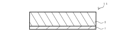
- FIG. 3 is a schematic cross-sectional view of a resin sheet according to Embodiment 1.
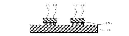
- FIG. It is a cross-sectional schematic diagram of the board
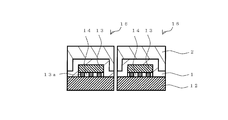
- FIG. It is a figure which shows typically a mode that the electronic device package was diced. It is a figure which shows typically a mode that the chip-shaped electronic device package was mounted in the board
- FIG. (A) is a cross-sectional schematic diagram of the resin sheet of Embodiment 2.
- FIG. (B) is a schematic bottom view thereof.
- FIG. 1 is a schematic cross-sectional view of a resin sheet 11 according to the first embodiment.
- the resin sheet 11 has a structure in which a first resin layer 1 and a second resin layer 2 are laminated.
- supports such as a polyethylene terephthalate (PET) film may be provided on both surfaces of the resin sheet 11.
- PET polyethylene terephthalate
- a release treatment may be applied to the support.
- the thermal conductivity of the first resin layer 1 is 1 W / mK or more. Since it is 1 W / mK or more, the heat of the electronic device can be released to the substrate through the first resin layer having high thermal conductivity.
- the thermal conductivity of the first resin layer 1 is preferably 3 W / mK or more.
- the upper limit of the heat conductivity of the 1st resin layer 1 is not specifically limited, For example, it is 15 W / mK or less.
- the first resin layer 1 is preferably electrically insulating.
- the first resin layer 1 preferably contains heat conductive particles. Thereby, thermal conductivity can be designed to be 1 W / mK or more.
- the heat conductive particles are not particularly limited, and examples thereof include electrically insulating particles such as alumina (aluminum oxide), zinc oxide, magnesium oxide, boron nitride, magnesium hydroxide, aluminum nitride, and silicon carbide. These can be used alone or in combination of two or more. Of these, alumina and boron nitride are preferred because of their high thermal conductivity and good fluidity.
- electrically insulating particles such as alumina (aluminum oxide), zinc oxide, magnesium oxide, boron nitride, magnesium hydroxide, aluminum nitride, and silicon carbide.
- the thermal conductivity of the thermal conductive particles is not particularly limited as long as thermal conductivity can be imparted to the first resin layer 1, but is preferably 12 W / mK or more, more preferably 15 W / mK or more, and still more preferably. Is 25 W / mK or more. When it is 12 W / mK or more, thermal conductivity of 1 W / mK or more can be easily imparted to the first resin layer 1.
- the heat conductivity of the heat conductive particles is, for example, 200 W / mK or less.
- the particle shape of the heat conductive particles is not particularly limited, and examples thereof include a spherical shape, an elliptical sphere shape, a flat shape, a needle shape, a fiber shape, a flake shape, a spike shape, and a coil shape. Of these shapes, a spherical shape is preferable in that it has excellent dispersibility and can improve the filling rate.
- the content of the heat conductive particles in the first resin layer 1 is preferably 55% by volume or more, more preferably 60% by volume or more.
- the heat conductivity of the 1st resin layer 1 can be improved as it is 55 volume% or more.
- the content of the heat conductive particles is preferably 83% by volume or less, more preferably 70% by volume or less. When the content is 83% by volume or less, a relative decrease in the adhesive component in the first resin layer 1 can be prevented, and wettability and adhesion to an electronic device or a substrate can be secured.
- the content of the heat conductive particles can be explained by using “wt%” as a unit. Typically, the content of alumina will be described with “wt%” as a unit. Since alumina usually has a specific gravity of 3.9 g / cm 3 , the preferred range of the alumina content (% by weight) is, for example, as follows. That is, the content of alumina in the first resin layer 1 is preferably 83% by weight or more, and more preferably 86% by weight or more. The content of alumina in the first resin layer 1 is preferably 95% by weight or less, and more preferably 90% by weight or less.
- the particle size distribution measured by the laser diffraction scattering method of the heat conductive particles when the total amount of the heat conductive particles is 100% by volume satisfies the following relationship.
- the ratio of particles having a particle size of more than 100 ⁇ m is 1% by volume or less, preferably 0.5% by volume or less, and more preferably 0.3% by volume or less.
- the lower limit of the ratio of particles having a particle size of more than 100 ⁇ m is preferably 0.01% by volume or more.
- the ratio of particles having a particle size of 10 ⁇ m or less is 30% to 70% by volume, preferably 35% to 65% by volume, and more preferably 40% to 60% by volume.
- the ratio of particles having a particle size of 1 ⁇ m or less is 10% by volume or more, preferably 13% by volume or more, and more preferably 15% by volume or more.
- the upper limit of the ratio of particles having a particle size of 1 ⁇ m or less is preferably 40% by volume or less.
- the particle size distribution can be derived by using a sample arbitrarily extracted from the population and measuring it using a laser diffraction / scattering particle size distribution measuring apparatus.
- the first resin layer 1 preferably contains an epoxy resin.
- the epoxy resin is not particularly limited.
- triphenylmethane type epoxy resin, cresol novolac type epoxy resin, biphenyl type epoxy resin, modified bisphenol A type epoxy resin, bisphenol A type epoxy resin, bisphenol F type epoxy resin, modified bisphenol F type epoxy resin, dicyclopentadiene type Various epoxy resins such as an epoxy resin, a phenol novolac type epoxy resin, and a phenoxy resin can be used. These epoxy resins may be used alone or in combination of two or more.
- the epoxy resin is solid at room temperature having an epoxy equivalent of 150 to 250 and a softening point or melting point of 50 to 130 ° C.
- triphenylmethane type epoxy resin, cresol novolac type epoxy resin, and biphenyl type epoxy resin are more preferable from the viewpoint of reliability.
- the first resin layer 1 preferably contains a phenol resin.
- the phenol resin is not particularly limited as long as it causes a curing reaction with the epoxy resin.
- a phenol novolac resin, a phenol aralkyl resin, a biphenyl aralkyl resin, a dicyclopentadiene type phenol resin, a cresol novolak resin, a resole resin, or the like is used.
- These phenolic resins may be used alone or in combination of two or more.
- phenolic resin those having a hydroxyl equivalent weight of 70 to 250 and a softening point of 50 to 110 ° C. are preferably used from the viewpoint of reactivity with the epoxy resin, and in particular, phenol novolak from the viewpoint of high curing reactivity. Resin can be used suitably. From the viewpoint of reliability, low hygroscopic materials such as phenol aralkyl resins and biphenyl aralkyl resins can also be suitably used.
- the total content of the epoxy resin and the phenol resin in the first resin layer 1 is preferably 5% by weight or more. Adhesive strength with respect to an electronic device, a board
- the total content of the epoxy resin and the phenol resin in the first resin layer 1 is preferably 20% by weight or less. If it is 20% by weight or less, the hygroscopicity can be kept low.
- the blending ratio of the epoxy resin and the phenol resin is blended so that the total of hydroxyl groups in the phenol resin is 0.7 to 1.5 equivalents with respect to 1 equivalent of the epoxy group in the epoxy resin from the viewpoint of curing reactivity. It is preferable to use 0.9 to 1.2 equivalents.
- the first resin layer 1 preferably contains a thermoplastic resin.
- Thermoplastic resins include natural rubber, butyl rubber, isoprene rubber, chloroprene rubber, ethylene-vinyl acetate copolymer, ethylene-acrylic acid copolymer, ethylene-acrylic acid ester copolymer, polybutadiene resin, polycarbonate resin, thermoplasticity.
- MBS resin methyl And methacrylate-butadiene-styrene copolymer
- the content of the thermoplastic resin in the first resin layer 1 is preferably 1% by weight or more.
- the content of the thermoplastic resin in the first resin layer 1 is preferably 10% by weight or less. Adhesive force with respect to an electronic device, a board
- the first resin layer 1 preferably contains a curing accelerator.
- the curing accelerator is not particularly limited as long as it can cure the epoxy resin and the phenol resin, and examples thereof include organophosphorus compounds such as triphenylphosphine and tetraphenylphosphonium tetraphenylborate; 2-phenyl-4, And imidazole compounds such as 5-dihydroxymethylimidazole and 2-phenyl-4-methyl-5-hydroxymethylimidazole.
- organophosphorus compounds such as triphenylphosphine and tetraphenylphosphonium tetraphenylborate
- 2-phenyl-4, And imidazole compounds such as 5-dihydroxymethylimidazole and 2-phenyl-4-methyl-5-hydroxymethylimidazole.
- the content of the curing accelerator is preferably 0.1 to 5 parts by weight with respect to 100 parts by weight of the total of the epoxy resin and the phenol resin.
- the 1st resin layer 1 may contain suitably the compounding agent generally used for manufacture of sealing resin other than the said component, for example, a silica etc. suitably.
- the first resin layer 1 can be manufactured by a general manufacturing method. For example, each of the above components is dissolved or dispersed in a solvent (for example, methyl ethyl ketone, ethyl acetate, etc.) to prepare a coating solution. After the coating solution is applied onto a substrate separator, the coating film is dried. Thereby, the 1st resin layer 1 is producible.
- a solvent for example, methyl ethyl ketone, ethyl acetate, etc.
- the thickness of the first resin layer 1 is preferably 200 ⁇ m or less, more preferably 100 ⁇ m or less. When the thickness is 100 ⁇ m or less, wear of the dicing blade can be reduced. Moreover, the thickness of the 1st resin layer 1 becomes like this. Preferably it is 40 micrometers or more, More preferably, it is 50 micrometers or more. When it is 40 ⁇ m or more, a thermal circuit (thermal conduction path) in parallel with electrical wiring such as bumps can be formed.
- the thermal conductivity of the second resin layer 2 is not particularly limited, but is preferably lower than the thermal conductivity of the first resin layer 1. This makes it easier for the heat of the electronic device to escape to the substrate.
- the thermal conductivity of the second resin layer 2 is preferably 3 W / mK or less, more preferably 1 W / mK or less.
- the minimum of the heat conductivity of the 2nd resin layer 2 is although it does not specifically limit, For example, it is 0.5 W / mK or more.
- the second resin layer 2 may be electrically insulating or not electrically insulating, but is preferably electrically insulating.
- the second resin layer 2 preferably contains an epoxy resin.
- an epoxy resin what was demonstrated in the 1st resin layer 1 can be used conveniently.
- the second resin layer 2 preferably contains a phenol resin.
- a phenol resin what was demonstrated in the 1st resin layer 1 can be used conveniently.
- the total content of the epoxy resin and the phenol resin in the second resin layer 2 is preferably 2% by weight or more. When it is 2% by weight or more, sufficient cured product strength can be obtained.
- the total content of the epoxy resin and the phenol resin in the second resin layer 2 is preferably 20% by weight or less, and more preferably 10% by weight or less. When it is 20% by weight or less, the linear expansion coefficient of the cured product can be reduced and moisture absorption can be reduced.
- the blending ratio of the epoxy resin and the phenol resin is blended so that the total of hydroxyl groups in the phenol resin is 0.7 to 1.5 equivalents with respect to 1 equivalent of the epoxy group in the epoxy resin from the viewpoint of curing reactivity. It is preferable to use 0.9 to 1.2 equivalents.
- the second resin layer 2 preferably contains a thermoplastic resin.
- a thermoplastic resin what was demonstrated by the 1st resin layer 1 can be used conveniently.
- the content of the thermoplastic resin in the second resin layer 2 is preferably 0.5% by weight or more, and more preferably 1% by weight or more. When it is 0.5% by weight or more, good flexibility is obtained.
- the content of the thermoplastic resin in the second resin layer 2 is preferably 3.5% by weight or less. Good fluidity
- the second resin layer 2 preferably contains a filler.
- an inorganic filler is preferable.
- the inorganic filler include quartz glass, talc, silica (such as fused silica and crystalline silica), alumina, aluminum nitride, silicon nitride, and boron nitride.
- silica and alumina are preferable, and silica is more preferable because the linear expansion coefficient can be satisfactorily reduced.
- Silica is preferably fused silica and more preferably spherical fused silica because it is excellent in fluidity.
- the average particle size of the filler is preferably 1 ⁇ m or more, more preferably 5 ⁇ m or more. When it is 1 ⁇ m or more, it is easy to obtain flexibility and flexibility of the resin sheet.
- the average particle size of the filler is preferably 40 ⁇ m or less, more preferably 30 ⁇ m or less. When it is 40 ⁇ m or less, it is easy to increase the filling rate of the filler.
- the average particle diameter can be derived, for example, by using a sample arbitrarily extracted from the population and measuring it using a laser diffraction / scattering particle size distribution measuring apparatus.
- the filler is preferably treated (pretreated) with a silane coupling agent. Thereby, wettability with resin can be improved and the dispersibility of a filler can be improved.
- the silane coupling agent is a compound having a hydrolyzable group and an organic functional group in the molecule.
- hydrolyzable group examples include an alkoxy group having 1 to 6 carbon atoms such as a methoxy group and an ethoxy group, an acetoxy group, and a 2-methoxyethoxy group.
- a methoxy group is preferable because it easily removes volatile components such as alcohol generated by hydrolysis.
- organic functional group examples include vinyl group, epoxy group, styryl group, methacryl group, acrylic group, amino group, ureido group, mercapto group, sulfide group, and isocyanate group.
- an epoxy group is preferable because it easily reacts with an epoxy resin or a phenol resin.
- silane coupling agent examples include vinyl group-containing silane coupling agents such as vinyltrimethoxysilane and vinyltriethoxysilane; 2- (3,4-epoxycyclohexyl) ethyltrimethoxysilane, 3-glycidoxypropylmethyl Epoxy group-containing silane coupling agents such as dimethoxysilane, 3-glycidoxypropyltrimethoxysilane, 3-glycidoxypropylmethyldiethoxysilane, 3-glycidoxypropyltriethoxysilane; p-styryltrimethoxysilane, etc.
- vinyl group-containing silane coupling agents such as vinyltrimethoxysilane and vinyltriethoxysilane
- 2- (3,4-epoxycyclohexyl) ethyltrimethoxysilane 3-glycidoxypropylmethyl Epoxy group-containing silane coupling agents such as dimethoxysilane, 3-glycidoxypropyl
- Styryl group-containing silane coupling agent 3-methacryloxypropylmethyldimethoxysilane, 3-methacryloxypropyltrimethoxysilane, 3-methacryloxypropylmethyldiethoxysilane, 3-methacryloxypropyltri Methacrylic group-containing silane coupling agents such as toxisilane; Acrylic group-containing silane coupling agents such as 3-acryloxypropyltrimethoxysilane; N-2- (aminoethyl) -3-aminopropylmethyldimethoxysilane, N-2- (Aminoethyl) -3-aminopropyltrimethoxysilane, 3-aminopropyltrimethoxysilane, 3-aminopropyltriethoxysilane, 3-triethoxysilyl-N- (1,3-dimethyl-butylidene) propylamine, N Amino group-containing silane coupling agents such as phenyl-3-a
- the method for treating the filler with the silane coupling agent is not particularly limited, and examples include a wet method in which the filler and the silane coupling agent are mixed in a solvent, and a dry method in which the filler and the silane coupling agent are treated in a gas phase. It is done.
- the treatment amount of the silane coupling agent is not particularly limited, but it is preferable to treat 0.1 to 1 part by weight of the silane coupling agent with respect to 100 parts by weight of the untreated filler.
- the content of the filler in the second resin layer 2 is preferably 70% by volume or more, and more preferably 74% by volume or more.
- a linear expansion coefficient can be designed low as it is 70 volume% or more.
- the filler content is preferably 90% by volume or less, more preferably 85% by volume or less.
- liquidity, and adhesiveness are favorably obtained as it is 90 volume% or less.
- the filler content can also be explained by using “% by weight” as a unit. Typically, the content of silica will be described in units of “% by weight”. Since silica usually has a specific gravity of 2.2 g / cm 3 , the preferred range of the silica content (% by weight) is, for example, as follows. That is, the content of silica in the second resin layer 2 is preferably 81% by weight or more, and more preferably 84% by weight or more. The content of silica in the second resin layer 2 is preferably 94% by weight or less, and more preferably 91% by weight or less.
- the preferred range of the alumina content is, for example, as follows. That is, the content of alumina in the second resin layer 2 is preferably 88% by weight or more, and more preferably 90% by weight or more. The content of alumina in the second resin layer 2 is preferably 97% by weight or less, and more preferably 95% by weight or less.
- the second resin layer 2 preferably contains a curing accelerator.
- a hardening accelerator what was demonstrated in the 1st resin layer 1 can be used conveniently.
- the content of the curing accelerator is preferably 0.1 to 5 parts by weight with respect to 100 parts by weight of the total of the epoxy resin and the phenol resin.
- the second resin layer 2 may appropriately contain a compounding agent generally used in the production of a sealing resin, for example, a flame retardant component, a pigment, a silane coupling agent, and the like.
- a compounding agent generally used in the production of a sealing resin for example, a flame retardant component, a pigment, a silane coupling agent, and the like.
- the flame retardant component for example, various metal hydroxides such as aluminum hydroxide, magnesium hydroxide, iron hydroxide, calcium hydroxide, tin hydroxide, complex metal hydroxide, phosphazene compounds, and the like can be used. Of these, phosphazene compounds are preferred because they are excellent in flame retardancy and strength after curing.
- the pigment is not particularly limited, and examples thereof include carbon black.
- the manufacturing method of the 2nd resin layer 2 is not specifically limited,
- mixing said each component for example, an epoxy resin, a phenol resin, a thermoplastic resin, a filler, and a hardening accelerator
- a processing method is preferred. Thereby, a filler can be filled highly and a linear expansion coefficient can be designed low.
- a kneaded material is prepared by melting and kneading an epoxy resin, a phenol resin, a thermoplastic resin, a filler, and a curing accelerator with a known kneader such as a mixing roll, a pressure kneader, or an extruder.
- the kneaded material is plastically processed into a sheet shape.
- the upper limit of the temperature is preferably 140 ° C. or less, and more preferably 130 ° C. or less.
- the lower limit of the temperature is preferably equal to or higher than the softening point of each component described above, for example, 30 ° C or higher, and preferably 50 ° C or higher.
- the kneading time is preferably 1 to 30 minutes.
- the kneading is preferably performed under reduced pressure conditions (under reduced pressure atmosphere), and the pressure under reduced pressure conditions is, for example, 1 ⁇ 10 ⁇ 4 to 0.1 kg / cm 2 .
- the kneaded material after melt-kneading is preferably subjected to plastic working in a high temperature state without cooling.
- the plastic working method is not particularly limited, and examples thereof include a flat plate pressing method, a T die extrusion method, a screw die extrusion method, a roll rolling method, a roll kneading method, an inflation extrusion method, a coextrusion method, and a calendering method.
- the plastic working temperature is preferably not less than the softening point of each component described above, and is 40 to 150 ° C., preferably 50 to 140 ° C., more preferably 70 to 120 ° C. in consideration of the thermosetting property and moldability of the epoxy resin. is there.
- the thickness of the second resin layer 2 is not particularly limited, but is preferably 20 ⁇ m or more, more preferably 50 ⁇ m or more. Moreover, the thickness of the 2nd resin layer 2 becomes like this. Preferably it is 2000 micrometers or less, More preferably, it is 1000 micrometers or less. An electronic device can be favorably sealed as it is in the said range.
- the thermal conductivity of the first resin layer 1 / the thermal conductivity of the second resin layer 2 is preferably 2 or more, more preferably 3 or more. When it is 2 or more, the heat of the electronic device can be effectively released to the substrate.
- the upper limit of the value of the heat conductivity of the 1st resin layer 1 / the heat conductivity of the 2nd resin layer 2 is not specifically limited, For example, it is 10 or less.
- the thickness of the first resin layer 1 / the thickness of the second resin layer 2 (ratio of the thickness of the first resin layer 1 to the thickness of the second resin layer 2) is preferably 10 or less, more preferably 5 or less. When it is 10 or less, it is possible to reduce the wear of the dicing blade while effectively releasing the heat of the electronic device to the substrate.
- the thickness of the first resin layer 1 / the thickness of the second resin layer 2 is preferably 1 or more. When the number is 1 or more, warpage of the electronic device package can be reduced.
- the 1st resin layer 1 is a single layer is shown in FIG. 1, the 1st resin layer 1 is not limited to this, A multilayer may be sufficient.
- the 2nd resin layer 2 is a single layer is shown in FIG. 1, the 2nd resin layer 2 is not limited to this, A multilayer may be sufficient.
- Resin sheet 11 is used for sealing electronic devices.
- Electronic devices include sensors, MEMS (Micro Electro Mechanical Systems), SAW (Surface Acoustic Wave) filters and other electronic devices (hollow electronic devices); semiconductor chips, ICs (integrated circuits), semiconductors such as transistors Examples include an element, a capacitor, and a resistor.
- the hollow structure refers to a hollow portion formed between the electronic device and the substrate when the electronic device is mounted on the substrate.
- the sealing method is not particularly limited, and examples thereof include a method of covering an electronic device mounted on a substrate with a resin sheet 11 and a method of covering an electronic device mounted on an adhesive sheet with a resin sheet 11. It does not specifically limit as a board
- substrate For example, a printed wiring board, a ceramic substrate, a silicon substrate, a metal substrate, a semiconductor wafer etc. are mentioned.
- an electronic device package can be obtained by performing the following steps.
- the following steps are commonly referred to as chip-on-wafer (COW) processes.
- COW chip-on-wafer
- a substrate 12 on which a plurality of electronic devices 13 are mounted is prepared (see FIG. 2).
- a known apparatus such as a flip chip bonder or a die bonder can be used.
- the electronic device 13 and the substrate 12 are electrically connected.
- FIG. 2 shows an example in which the electronic device 13 and the substrate 12 are electrically connected via protruding electrodes 13a such as bumps.
- the electronic device 13 is a hollow electronic device such as a SAW filter
- a hollow portion (hollow structure) 14 is maintained between the electronic device 13 and the substrate 12.
- the distance between the electronic device 13 and the substrate 12 is generally about 15 to 50 ⁇ m.
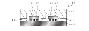
- the sealing step the resin sheet 11 is laminated on the substrate 12 so that the first resin layer 1 is in contact with the substrate 12 and the electronic device 13, and the electronic device 13 is sealed with the resin sheet 11 (see FIG. 3). ). Thereby, the electronic device package 15 in which the electronic device 13 is sealed with resin is obtained.
- the method for laminating the resin sheet 11 on the substrate 12 is not particularly limited, and can be performed by a known method such as hot pressing or laminator.
- the temperature is, for example, 40 to 100 ° C., preferably 50 to 90 ° C.
- the pressure is, for example, 0.1 to 10 MPa, preferably 0.5 to 8 MPa
- the time is, for example, 0.3 to 10 minutes, preferably 0.5 to 5 minutes.
- it is preferable to press under reduced pressure conditions for example, 0.1 to 5 kPa).
- thermosetting process If necessary, the resin sheet 11 of the electronic device package 15 is thermoset.
- the heating temperature is preferably 100 ° C or higher, more preferably 120 ° C or higher.
- the upper limit of the heating temperature is preferably 200 ° C. or lower, more preferably 180 ° C. or lower.
- the heating time is preferably 10 minutes or more, more preferably 30 minutes or more.
- the upper limit of the heating time is preferably 180 minutes or less, more preferably 120 minutes or less.
- you may pressurize as needed Preferably it is 0.1 Mpa or more, More preferably, it is 0.5 Mpa or more.
- the upper limit is preferably 10 MPa or less, more preferably 5 MPa or less.
- the resin sheet 11 of the electronic device package 15 is ground.
- the grinding method include a grinding method using a grindstone that rotates at high speed.
- the substrate 12 of the electronic device package 15 is ground.
- the grinding method include a grinding method using a grindstone that rotates at high speed.
- vias (Via) are formed in the electronic device package 15 as necessary.
- rewiring is formed in the electronic device package 15 as necessary.
- bumps are formed on the rewiring as necessary.
- the electronic device package 15 is diced (see FIG. 4). Thereby, the chip-shaped electronic device package 16 can be obtained.
- Laser marking can be performed on the electronic device package 15 or the electronic device package 16 at an arbitrary timing. For example, laser marking may be performed on the electronic device package 15 before thermosetting, laser marking may be performed on the electronic device package 15 after thermosetting, or laser marking may be performed on the electronic device package 16.
- the first resin layer 1 having high thermal conductivity is in contact with the electronic device 13
- the heat generated in the electronic device 13 is transferred to the substrate 12 or the like (for example, the substrate 12, Board 18, housing, etc.). Therefore, hot spots can be eliminated.
- an electronic device package can be obtained by performing the following steps. The following steps are suitable for manufacturing a fan-out type wafer level package (WLP).
- WLP fan-out type wafer level package
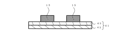
- Step of fixing the electronic device to the adhesive sheet First, the some electronic device 13 is fixed to the adhesive sheet 41 (refer FIG. 6). At this time, if necessary, the electronic device 13 is arranged and fixed so that the circuit forming surface of the electronic device 13 faces the adhesive sheet 41.
- a known apparatus such as a flip chip bonder or a die bonder can be used.
- the pressure-sensitive adhesive sheet 41 usually has a support 42 and a pressure-sensitive adhesive layer 43 laminated on the support 42.
- the pressure-sensitive adhesive layer 43 is not particularly limited, but a heat-peelable pressure-sensitive adhesive layer, a radiation curable pressure-sensitive adhesive layer, or the like is usually used because it can be easily peeled off.
- the material for the support 42 is not particularly limited. For example, metal materials such as SUS, plastic materials such as polyimide, polyamideimide, polyetheretherketone, and polyethersulfone.
- the method for laminating the resin sheet 11 on the pressure-sensitive adhesive sheet 41 is not particularly limited, and can be performed by a known method such as hot pressing or laminator.
- the sealing body 51 is thermoset (the resin sheet 11 of the sealing body 51 is thermoset).
- the adhesive sheet 41 is peeled from the sealing body 51 (see FIG. 8).
- the peeling method is not particularly limited, it is preferable to peel the adhesive layer 43 after reducing the adhesive strength.
- the pressure-sensitive adhesive layer 43 is a heat-peelable pressure-sensitive adhesive layer, the pressure-sensitive adhesive layer 43 is heated and peeled after the pressure-sensitive adhesive force of the pressure-sensitive adhesive layer 43 is reduced.
- the resin sheet 11 of the sealing body 51 is ground as needed (refer FIG. 9).
- the grinding method include a grinding method using a grindstone that rotates at high speed.
- the rewiring 52 is formed in the sealing body 51 using a semi-additive method or the like (see FIG. 10).
- an insulating layer such as polyimide or polybenzoxazole (PBO) is formed on the surface of the sealing body 51 where the rewiring 52 is formed.
- the insulating layer can be formed, for example, by laminating a film such as a dry film resist.
- the bumping process can be performed by a known method such as solder ball or solder plating.
- Dicing process Dicing of the sealing body 51 including elements such as the electronic device 13, the first resin layer 1, and the rewiring 52 may be performed (see FIG. 11). As described above, it is possible to obtain the electronic device package 61 in which the wiring is drawn outside the chip region. In addition, you may use the sealing body 51 as an electronic device package as it is, without dicing.
- the electronic device package 61 is mounted on the substrate as necessary.
- Laser marking can be performed on the sealing body 51 or the electronic device package 61 at an arbitrary timing. For example, laser marking may be performed on the sealing body 51 before thermosetting, laser marking may be performed on the sealing body 51 after thermosetting, or laser marking may be performed on the electronic device package 61.
- the heat generated in the electronic device 13 is released to a substrate or the like (for example, a substrate or a housing). Can do. Therefore, hot spots can be eliminated.
- the heat generated in the electronic device 13 can be transmitted to the substrate via the first resin layer 1, the rewiring 52, the bump 53, and the like.
- the electronic device package 61 can be suitably applied to mounting methods such as package on package (PoP), system in package (SiP), and multichip package (MCP).
- PoP package on package
- SiP system in package
- MCP multichip package
- TMV through mold via
- positioned on the 1st resin layer 1 was demonstrated.
- the resin sheet includes a first resin layer 1, a third layer disposed on the first resin layer 1, and a second resin layer 2 disposed on the third layer. Is provided.
- the resin sheet includes a first resin layer 1, a second resin layer 2 disposed on the first resin layer 1, and a third resin disposed on the second resin layer 2. And a layer.
- a layer containing a resin, a metal layer, and the like are suitable.
- the third layer may be a single layer or multiple layers.
- FIG. 12A is a schematic cross-sectional view of the resin sheet 101 of the second embodiment.
- (B) is a schematic bottom view thereof.
- 101 is the same as the resin sheet 11 of the first embodiment.
- the thermally conductive particles are very hard and cause wear of the dicing blade.
- the resin sheet 101 includes the resin layer 31 at the portion to be diced, wear of the dicing blade can be reduced.
- parts other than the resin layer 31 are high thermal conductivity, the heat
- the content of the heat conductive particles in the resin layer 31 is 30% by volume or less, preferably 0% by volume. Since it is 30 volume% or less, abrasion of a dicing blade can be reduced.
- the resin layer 31 preferably contains an epoxy resin.
- an epoxy resin what was demonstrated in the 1st resin layer 1 can be used conveniently.
- the resin layer 31 preferably contains a phenol resin.
- a phenol resin what was demonstrated in the 1st resin layer 1 can be used conveniently.
- the blending ratio of the epoxy resin and the phenol resin is blended so that the total of hydroxyl groups in the phenol resin is 0.7 to 1.5 equivalents with respect to 1 equivalent of the epoxy group in the epoxy resin from the viewpoint of curing reactivity. It is preferable to use 0.9 to 1.2 equivalents.
- the resin layer 31 preferably contains a thermoplastic resin.
- a thermoplastic resin what was demonstrated by the 1st resin layer 1 can be used conveniently.
- the resin layer 31 preferably contains a filler. As a filler, what was demonstrated by the 2nd resin layer 2 can be used conveniently.
- the resin layer 31 preferably contains a curing accelerator.
- a hardening accelerator what was demonstrated in the 1st resin layer 1 can be used conveniently.
- the method for forming the resin layer 31 on the dicing scheduled portion of the first resin layer 1 is not particularly limited.
- the resin layer 31 is removed from the first resin layer 1 to provide a space, and the resin layer is formed in the space.
- the resin layer 31 can be formed by filling the solution for forming 31 and drying.
- positioned on the 1st resin layer 1 was demonstrated.
- the resin sheet includes a first resin layer 1, a third layer disposed on the first resin layer 1, and a second resin layer 2 disposed on the third layer. Is provided.
- the resin sheet includes a first resin layer 1, a second resin layer 2 disposed on the first resin layer 1, and a third resin disposed on the second resin layer 2. And a layer.
- a layer containing a resin, a metal layer, and the like are suitable.
- the third layer may be a single layer or multiple layers.
- Epoxy resin YSLV-80XY manufactured by Nippon Steel Chemical Co., Ltd. (bisphenol F type epoxy resin, epkin equivalent 200 g / eq. Softening point 80 ° C.)
- Phenolic resin MEH-7851-SS (phenol resin having a biphenylaralkyl skeleton, hydroxyl group equivalent 203 g / eq. Softening point 67 ° C.) manufactured by Meiwa Kasei Co., Ltd.
- Thermoplastic resin Metablene C-132E manufactured by Mitsubishi Rayon Co., Ltd.
- Epoxy resin YSLV-80XY manufactured by Nippon Steel Chemical Co., Ltd. (bisphenol F type epoxy resin, epkin equivalent 200 g / eq. Softening point 80 ° C.)
- Phenolic resin MEH-7851-SS (phenol resin having a biphenylaralkyl skeleton, hydroxyl group equivalent 203 g / eq. Softening point 67 ° C.) manufactured by Meiwa Kasei Co., Ltd.
- Thermoplastic resin Metablene C-132E manufactured by Mitsubishi Rayon Co., Ltd.
- a varnish similar to the first resin layer was prepared except that the amount of heat conductive particles described in Table 3 was used. After removing the resin layer of the dicing scheduled portion from the first resin layer to provide a space, the space was filled with varnish and dried to form a resin layer in the dicing planned portion of the first resin layer. .
- the resin layer in the portion to be diced is different from the resin layer other than the portion to be diced only in the amount of thermally conductive particles.
- Samples (first resin layer and second resin layer) were heat-cured by heat treatment at 175 ° C. for 1 hour in a dryer. Thereafter, the thermal diffusivity ⁇ (m 2 / s) of the sample was measured by a TWA method (temperature wave thermal analysis method, measuring device; Eye Phase Mobile, manufactured by Eye Phase Co., Ltd.). Next, the specific heat Cp (J / g ⁇ ° C.) of the sample was measured by the DSC method. Specific heat measurement was performed using DSC 6220 manufactured by SII Nano Technology Co., Ltd.
- thermal conductivity was calculated by the following formula.
- a resin sheet is laminated on a ceramic substrate on which SAW filters (chip thickness: 200 ⁇ m, bump height: 20 ⁇ m) are arranged in a matrix, and vacuum pressing is performed for 1 minute at a temperature of 100 ° C. and a pressure of 300 kPa (final vacuum degree 6.65). ⁇ 10 2 Pa).
- the resin sheet was cured by placing the SAW filter package in an oven at 130 ° C. for 3 hours. Thereafter, the SAW filter package was separated into pieces using a dicing apparatus. After dicing, the amount of wear of the dicing blade was measured and determined by a contact type blade alignment function of a dicing apparatus (DFD6361, manufactured by DISCO). The case where the amount of wear was less than 30 ⁇ m was judged as ⁇ , and the case where the amount of wear was 30 ⁇ m or more was judged as x.
- DMD6361 contact type blade alignment function of a dicing apparatus
- a resin sheet is laminated on a ceramic substrate on which SAW filters (chip thickness: 200 ⁇ m, bump height: 20 ⁇ m) are arranged in a matrix, and vacuum pressing is performed for 1 minute at a temperature of 100 ° C. and a pressure of 300 kPa (final vacuum degree 6.65). ⁇ 10 2 Pa). After opening to the atmosphere, the resin sheet was cured by placing the SAW filter package in an oven at 130 ° C. for 3 hours. Thereafter, the SAW filter package was separated into pieces using a dicing apparatus. A drive test was performed on the separated SAW filter using a SAW filter test apparatus.
- the temperature distribution (hot spot) on the surface of the SAW filter was measured for the SAW filter being driven using infrared thermography. And the case where the temperature of a hot spot part was less than +10 degreeC from the lowest temperature part of the package surface was evaluated as (circle), and the case where a hot spot area was +10 degreeC or more was determined as x.
- the substrate was cut into 5 mm ⁇ 5 mm pieces, the pieces were placed on the surface of the resin sheet, and vacuum pressed (attainment vacuum degree 6.65 ⁇ 10 2 Pa) for 1 minute under conditions of a temperature of 100 ° C. and a pressure of 300 kPa. . Then, the resin sheet was hardened by putting in 130 degreeC oven for 3 hours. After curing, the shear adhesive strength of the substrate was measured using a universal bond tester (Dage 4000) manufactured by Dage. A case where the shear adhesive strength of the element was 8 MPa or more and the shear adhesive strength of the substrate was 8 MPa or more was judged as ⁇ . The case where the shear adhesive strength of the element or the shear adhesive strength of the substrate was less than 8 MPa was determined as x.
- Dage 4000 universal bond tester
Landscapes
- Structures Or Materials For Encapsulating Or Coating Semiconductor Devices Or Solid State Devices (AREA)
- Cooling Or The Like Of Semiconductors Or Solid State Devices (AREA)
Abstract
電子デバイスの熱を基板に逃がすことができる電子デバイス封止用樹脂シート及び電子デバイスパッケージの製造方法を提供する。 本発明は、第1の樹脂層及び第2の樹脂層を備え、前記第1の樹脂層の熱伝導率が1W/mK以上である電子デバイス封止用樹脂シートに関する。
Description
本発明は、電子デバイス封止用樹脂シート及び電子デバイスパッケージの製造方法に関する。
従来、電子デバイスパッケージの製造方法として、基板などに固定された1又は複数の電子デバイスを封止樹脂で封止するという方法が知られている。このような封止樹脂として、例えば、熱硬化性樹脂シートが知られている(例えば、特許文献1参照)。
スマートフォンなどに使用される電子デバイスは高速で動作するため、電子デバイス及びその周辺が高温になり易い(ホットスポットが発生し易い)。電子デバイスが高温になると、動作が不安定になったり、電子デバイスの特性が劣化することがある。
しかしながら、特許文献1ではホットスポットの解消について検討されておらず、特許文献1に記載の熱硬化性樹脂シートはホットスポットを解消できない。
本発明は前記課題を解決し、電子デバイスの熱を基板に逃がすことができる電子デバイス封止用樹脂シート及び電子デバイスパッケージの製造方法を提供することを目的とする。
本発明は、第1の樹脂層及び第2の樹脂層を備え、前記第1の樹脂層の熱伝導率が1W/mK以上である電子デバイス封止用樹脂シートに関する。
本発明の電子デバイス封止用樹脂シートで電子デバイスを封止することにより、電子デバイスの熱を高熱伝導率の第1の樹脂層を介して基板に逃がすことができ、ひいては、筐体に逃がすことができる。したがって、ホットスポットを解消できる。
本発明の電子デバイス封止用樹脂シートでは、高熱伝導率の第1の樹脂層が電子デバイスの熱を基板に逃がす役割を担っており、第2の樹脂層の熱伝導率は高める必要がない。つまり、ダイシングブレードの摩耗の原因となるアルミナなどの熱伝導粒子を樹脂シート全体に配合する必要がない。このため、ダイシングブレードの摩耗を低減することもできる。また、コストを低減できる。
前記第1の樹脂層は熱伝導粒子を含み、前記第1の樹脂層中の前記熱伝導粒子の含有量が60~85体積%であることが好ましい。熱伝導粒子の含有量が前記範囲内であると、第1の樹脂層1の熱伝導率を高めつつ、電子デバイスや基板に対する良好な濡れ性及び接着性を得ることができる。
前記熱伝導粒子がアルミナ及び/又は窒化ホウ素であることが好ましい。これにより、良好な熱伝導性と、良好な流動性が得られる。
前記熱伝導粒子の含有量が30体積%以下の樹脂層が、前記第1の樹脂層のダイシングが予定されている部分に形成されていることが好ましい。熱伝導粒子(特にアルミナ)は非常に硬く、ダイシングブレードの摩耗の原因となるが、熱伝導粒子の含有量が少ない又は熱伝導粒子を含まない樹脂層を、第1の樹脂層のダイシングが予定されている部分に設けることにより、ダイシングブレードの摩耗を低減できる。
本発明はまた、前記第1の樹脂層が電子デバイスと接触するように、前記電子デバイス封止用樹脂シートで前記電子デバイスを封止する工程を含む電子デバイスパッケージの製造方法に関する。
これにより得られる電子デバイスパッケージにおいて、高熱伝導率の第1の樹脂層が電子デバイスと接触しているので、電子デバイスで発生した熱を基板に逃がすことができる。
以下に実施形態を掲げ、本発明を詳細に説明するが、本発明はこれらの実施形態のみに限定されるものではない。
[実施形態1]
図1は、実施形態1の樹脂シート11の断面模式図である。樹脂シート11は、第1の樹脂層1と第2の樹脂層2とを積層した構造である。なお、樹脂シート11の両面には、ポリエチレンテレフタレート(PET)フィルムなどの支持体が設けられていてもよい。樹脂シート11からの剥離を容易に行うために、支持体には離型処理が施されていてもよい。
図1は、実施形態1の樹脂シート11の断面模式図である。樹脂シート11は、第1の樹脂層1と第2の樹脂層2とを積層した構造である。なお、樹脂シート11の両面には、ポリエチレンテレフタレート(PET)フィルムなどの支持体が設けられていてもよい。樹脂シート11からの剥離を容易に行うために、支持体には離型処理が施されていてもよい。
第1の樹脂層1の熱伝導率は1W/mK以上である。1W/mK以上であるので、電子デバイスの熱を高熱伝導率の第1の樹脂層を介して基板に逃がすことができる。第1の樹脂層1の熱伝導率は好ましくは3W/mK以上である。第1の樹脂層1の熱伝導率の上限は特に限定されないが、例えば15W/mK以下である。
なお、第1の樹脂層1は、電気絶縁性であることが好ましい。
第1の樹脂層1は、熱伝導粒子を含むことが好ましい。これにより、熱伝導率を1W/mK以上に設計できる。
熱伝導粒子としては特に限定されず、例えば、アルミナ(酸化アルミニウム)、酸化亜鉛、酸化マグネシウム、窒化ホウ素、水酸化マグネシウム、窒化アルミニウム、炭化珪素等の電気絶縁性のものが挙げられる。これらは、単独で又は2種以上を併用して用いることができる。なかでも、熱伝導率が高く、良好な流動性が得られるという理由から、アルミナ、窒化ホウ素が好ましい。
熱伝導粒子の熱伝導率は、第1の樹脂層1に熱伝導性を付与可能な限り特に限定されないが、好ましくは12W/mK以上であり、より好ましくは15W/mK以上であり、さらに好ましくは25W/mK以上である。12W/mK以上であると、第1の樹脂層1に1W/mK以上の熱伝導性を容易に付与できる。熱伝導粒子の熱伝導率は、例えば、200W/mK以下である。
熱伝導粒子の粒子形状は特に限定されず、例えば、球状、楕円球体状、扁平形状、針状、繊維状、フレーク状、スパイク状、コイル状等が挙げられる。これらの形状のうち、分散性に優れ、充填率を向上できる点で球状が好ましい。
第1の樹脂層1中の熱伝導粒子の含有量は好ましくは55体積%以上、より好ましくは60体積%以上である。55体積%以上であると、第1の樹脂層1の熱伝導率を高めることができる。一方、熱伝導粒子の含有量は、好ましくは83体積%以下、より好ましくは70体積%以下である。83体積%以下であると、第1の樹脂層1中の接着成分の相対的な減少を防止でき、電子デバイスや基板に対する濡れ性及び接着性を確保できる。
熱伝導粒子の含有量は、「重量%」を単位としても説明できる。代表的にアルミナの含有量について、「重量%」を単位として説明する。
アルミナは通常、比重3.9g/cm3であるので、アルミナの含有量(重量%)の好適範囲は例えば以下のとおりである。
すなわち、第1の樹脂層1中のアルミナの含有量は、83重量%以上が好ましく、86重量%以上がより好ましい。第1の樹脂層1中のアルミナの含有量は、95重量%以下が好ましく、90重量%以下がより好ましい。
アルミナは通常、比重3.9g/cm3であるので、アルミナの含有量(重量%)の好適範囲は例えば以下のとおりである。
すなわち、第1の樹脂層1中のアルミナの含有量は、83重量%以上が好ましく、86重量%以上がより好ましい。第1の樹脂層1中のアルミナの含有量は、95重量%以下が好ましく、90重量%以下がより好ましい。
第1の樹脂層1では、熱伝導粒子の全量を100体積%とした際の熱伝導粒子のレーザー回折散乱法により測定した粒度分布が以下の関係を満たすことが好ましい。
100μm超:1体積%以下
10μm以下:30体積%以上70体積%以下
1μm以下:10体積%以上
100μm超:1体積%以下
10μm以下:30体積%以上70体積%以下
1μm以下:10体積%以上
該粒度分布において、粒径が100μm超の粒子の比率は1体積%以下であり、0.5体積%以下が好ましく、0.3体積%以下がより好ましい。なお、粒径が100μm超の粒子の比率の下限は0.01体積%以上が好ましい。粒径が10μm以下の粒子の比率は30体積%以上70体積%以下であり、35体積%以上65体積%以下が好ましく、40体積%以上60体積%以下がより好ましい。さらに、粒径が1μm以下の粒子の比率は10体積%以上であり、13体積%以上が好ましく、15体積%以上がより好ましい。なお、粒径が1μm以下の粒子の比率の上限は40体積%以下が好ましい。粒度分布が上記特定の関係にあることにより、中空構造付近における樹脂へダイラタンシー様作用を付与して封止時の中空構造への樹脂進入を好適に抑制することができる。粒度分布は、母集団から任意に抽出される試料を用い、レーザー回折散乱式粒度分布測定装置を用いて測定することにより導き出すことができる。
第1の樹脂層1は、エポキシ樹脂を含むことが好ましい。
エポキシ樹脂としては、特に限定されるものではない。例えば、トリフェニルメタン型エポキシ樹脂、クレゾールノボラック型エポキシ樹脂、ビフェニル型エポキシ樹脂、変性ビスフェノールA型エポキシ樹脂、ビスフェノールA型エポキシ樹脂、ビスフェノールF型エポキシ樹脂、変性ビスフェノールF型エポキシ樹脂、ジシクロペンタジエン型エポキシ樹脂、フェノールノボラック型エポキシ樹脂、フェノキシ樹脂などの各種のエポキシ樹脂を用いることができる。これらエポキシ樹脂は単独で用いてもよいし2種以上併用してもよい。
エポキシ樹脂の反応性を確保する観点からは、エポキシ当量150~250、軟化点もしくは融点が50~130℃の常温で固形のものが好ましい。なかでも、信頼性の観点から、トリフェニルメタン型エポキシ樹脂、クレゾールノボラック型エポキシ樹脂、ビフェニル型エポキシ樹脂がより好ましい。
第1の樹脂層1は、フェノール樹脂を含むことが好ましい。
フェノール樹脂は、エポキシ樹脂との間で硬化反応を生起するものであれば特に限定されるものではない。例えば、フェノールノボラック樹脂、フェノールアラルキル樹脂、ビフェニルアラルキル樹脂、ジシクロペンタジエン型フェノール樹脂、クレゾールノボラック樹脂、レゾール樹脂などが用いられる。これらフェノール樹脂は単独で用いてもよいし、2種以上併用してもよい。
フェノール樹脂としては、エポキシ樹脂との反応性の観点から、水酸基当量が70~250、軟化点が50~110℃のものを用いることが好ましく、なかでも硬化反応性が高いという観点から、フェノールノボラック樹脂を好適に用いることができる。また、信頼性の観点から、フェノールアラルキル樹脂やビフェニルアラルキル樹脂のような低吸湿性のものも好適に用いることができる。
第1の樹脂層1中のエポキシ樹脂及びフェノール樹脂の合計含有量は、5重量%以上が好ましい。5重量%以上であると、電子デバイス、基板などに対する接着力が良好に得られる。第1の樹脂層1中のエポキシ樹脂及びフェノール樹脂の合計含有量は、20重量%以下が好ましい。20重量%以下であると、吸湿性を低く抑えることができる。
エポキシ樹脂とフェノール樹脂の配合割合は、硬化反応性という観点から、エポキシ樹脂中のエポキシ基1当量に対して、フェノール樹脂中の水酸基の合計が0.7~1.5当量となるように配合することが好ましく、より好ましくは0.9~1.2当量である。
第1の樹脂層1は、熱可塑性樹脂を含むことが好ましい。
熱可塑性樹脂としては、天然ゴム、ブチルゴム、イソプレンゴム、クロロプレンゴム、エチレン-酢酸ビニル共重合体、エチレン-アクリル酸共重合体、エチレン-アクリル酸エステル共重合体、ポリブタジエン樹脂、ポリカーボネート樹脂、熱可塑性ポリイミド樹脂、6-ナイロンや6,6-ナイロンなどのポリアミド樹脂、フェノキシ樹脂、アクリル樹脂、PETやPBTなどの飽和ポリエステル樹脂、ポリアミドイミド樹脂、フッ素樹脂、スチレン-イソブチレン-スチレンブロック共重合体、メチルメタクリレート-ブタジエン-スチレン共重合体(MBS樹脂)などが挙げられる。これらの熱可塑性樹脂は単独で、又は2種以上を併用して用いることができる。
第1の樹脂層1中の熱可塑性樹脂の含有量は、1重量%以上が好ましい。1重量%以上であると、柔軟性、可撓性を付与できる。第1の樹脂層1中の熱可塑性樹脂の含有量は、10重量%以下が好ましい。10重量%以下であると、電子デバイス、基板などに対する接着力が良好に得られる。
第1の樹脂層1は、硬化促進剤を含むことが好ましい。
硬化促進剤としては、エポキシ樹脂とフェノール樹脂の硬化を進行させるものであれば特に限定されず、例えば、トリフェニルホスフィン、テトラフェニルホスホニウムテトラフェニルボレートなどの有機リン系化合物;2-フェニル-4,5-ジヒドロキシメチルイミダゾール、2-フェニル-4-メチル-5-ヒドロキシメチルイミダゾールなどのイミダゾール系化合物;などが挙げられる。
硬化促進剤の含有量は、エポキシ樹脂及びフェノール樹脂の合計100重量部に対して0.1~5重量部が好ましい。
第1の樹脂層1は、前記成分以外にも、封止樹脂の製造に一般に使用される配合剤、例えば、シリカなどを適宜含有してよい。
第1の樹脂層1は一般的な製法で作製できる。例えば、前記各成分を溶媒(例えば、メチルエチルケトン、酢酸エチルなど)に溶解ないし分散させて塗布液を調製し、塗布液を基材セパレータ上に塗布した後、塗布膜を乾燥させる。これにより、第1の樹脂層1を作製できる。
第1の樹脂層1の厚みは、好ましくは200μm以下、より好ましくは100μm以下である。100μm以下であると、ダイシングブレードの摩耗を低減できる。また、第1の樹脂層1の厚みは、好ましくは40μm以上、より好ましくは50μm以上である。40μm以上であると、バンプなどの電気配線と並列した熱回路(熱伝導パス)を形成できる。
第2の樹脂層2の熱伝導率は特に限定されないが、第1の樹脂層1の熱伝導率より低いことが好ましい。これにより、電子デバイスの熱を基板に逃がし易くなる。
第2の樹脂層2の熱伝導率は、好ましくは3W/mK以下、より好ましくは1W/mK以下である。また、第2の樹脂層2の熱伝導率の下限は特に限定されないが、例えば0.5W/mK以上である。
第2の樹脂層2は、電気絶縁性であってもよいし、電気絶縁性でなくともよいが、電気絶縁性であることが好ましい。
第2の樹脂層2は、エポキシ樹脂を含むことが好ましい。エポキシ樹脂としては、第1の樹脂層1で説明したものを好適に使用できる。
第2の樹脂層2は、フェノール樹脂を含むことが好ましい。フェノール樹脂としては、第1の樹脂層1で説明したものを好適に使用できる。
第2の樹脂層2中のエポキシ樹脂及びフェノール樹脂の合計含有量は、2重量%以上が好ましい。2重量%以上であると、充分な硬化物強度が得られる。第2の樹脂層2中のエポキシ樹脂及びフェノール樹脂の合計含有量は、20重量%以下が好ましく、10重量%以下がより好ましい。20重量%以下であると、硬化物の線膨張係数を小さくでき、また低吸湿化できる。
エポキシ樹脂とフェノール樹脂の配合割合は、硬化反応性という観点から、エポキシ樹脂中のエポキシ基1当量に対して、フェノール樹脂中の水酸基の合計が0.7~1.5当量となるように配合することが好ましく、より好ましくは0.9~1.2当量である。
第2の樹脂層2は、熱可塑性樹脂を含むことが好ましい。熱可塑性樹脂としては、第1の樹脂層1で説明したものを好適に使用できる。
第2の樹脂層2中の熱可塑性樹脂の含有量は、0.5重量%以上が好ましく、1重量%以上がより好ましい。0.5重量%以上であると、良好な可とう性が得られる。第2の樹脂層2中の熱可塑性樹脂の含有量は、3.5重量%以下が好ましい。3.5重量%以下であると、良好な流動性が得られる。
第2の樹脂層2は、フィラーを含むことが好ましい。
フィラーとしては特に限定されないが、無機充填材が好ましい。無機充填材としては、例えば、石英ガラス、タルク、シリカ(溶融シリカや結晶性シリカなど)、アルミナ、窒化アルミニウム、窒化珪素、窒化ホウ素などが挙げられる。なかでも、線膨張係数を良好に低減できるという理由から、シリカ、アルミナが好ましく、シリカがより好ましい。シリカとしては、流動性に優れるという理由から、溶融シリカが好ましく、球状溶融シリカがより好ましい。
フィラーの平均粒径は、好ましくは1μm以上、より好ましくは5μm以上である。1μm以上であると、樹脂シートの可撓性、柔軟性を得易い。フィラーの平均粒径は、好ましくは40μm以下、より好ましくは30μm以下である。40μm以下であると、フィラーを高充填率化し易い。
なお、平均粒径は、例えば、母集団から任意に抽出される試料を用い、レーザー回折散乱式粒度分布測定装置を用いて測定することにより導き出すことができる。
なお、平均粒径は、例えば、母集団から任意に抽出される試料を用い、レーザー回折散乱式粒度分布測定装置を用いて測定することにより導き出すことができる。
フィラーは、シランカップリング剤により処理(前処理)されたものが好ましい。これにより、樹脂との濡れ性を向上でき、フィラーの分散性を高めることができる。
シランカップリング剤は、分子中に加水分解性基及び有機官能基を有する化合物である。
加水分解性基としては、例えば、メトキシ基、エトキシ基などの炭素数1~6のアルコキシ基、アセトキシ基、2-メトキシエトキシ基等が挙げられる。なかでも、加水分解によって生じるアルコールなどの揮発成分を除去し易いという理由から、メトキシ基が好ましい。
有機官能基としては、ビニル基、エポキシ基、スチリル基、メタクリル基、アクリル基、アミノ基、ウレイド基、メルカプト基、スルフィド基、イソシアネート基などが挙げられる。なかでも、エポキシ樹脂、フェノール樹脂と反応し易いという理由から、エポキシ基が好ましい。
シランカップリング剤としては、例えば、ビニルトリメトキシシラン、ビニルトリエトキシシランなどのビニル基含有シランカップリング剤;2-(3,4-エポキシシクロヘキシル)エチルトリメトキシシラン、3-グリシドキシプロピルメチルジメトキシシラン、3-グリシドキシプロピルトリメトキシシラン、3-グリシドキシプロピルメチルジエトキシシラン、3-グリシドキシプロピルトリエトキシシランなどのエポキシ基含有シランカップリング剤;p-スチリルトリメトキシシランなどのスチリル基含有シランカップリング剤;3-メタクリロキシプロピルメチルジメトキシシラン、3-メタクリロキシプロピルトリメトキシシラン、3-メタクリロキシプロピルメチルジエトキシシラン、3-メタクリロキシプロピルトリエトキシシランなどのメタクリル基含有シランカップリング剤;3-アクリロキシプロピルトリメトキシシランなどのアクリル基含有シランカップリング剤;N-2-(アミノエチル)-3-アミノプロピルメチルジメトキシシラン、N-2-(アミノエチル)-3-アミノプロピルトリメトキシシラン、3-アミノプロピルトリメトキシシラン、3-アミノプロピルトリエトキシシラン、3-トリエトキシシリル-N-(1,3-ジメチル-ブチリデン)プロピルアミン、N-フェニル-3-アミノプロピルトリメトキシシラン、N-(ビニルベンジル)-2-アミノエチル-3-アミノプロピルトリメトキシシランなどのアミノ基含有シランカップリング剤;3-ウレイドプロピルトリエトキシシランなどのウレイド基含有シランカップリング剤;3-メルカプトプロピルメチルジメトキシシラン、3-メルカプトプロピルトリメトキシシランなどのメルカプト基含有シランカップリング剤;ビス(トリエトキシシリルプロピル)テトラスルフィドなどのスルフィド基含有シランカップリング剤;3-イソシアネートプロピルトリエトキシシランなどのイソシアネート基含有シランカップリング剤などが挙げられる。
シランカップリング剤によりフィラーを処理する方法としては特に限定されず、溶媒中でフィラーとシランカップリング剤を混合する湿式法、気相中でフィラーとシランカップリング剤を処理させる乾式法などが挙げられる。
シランカップリング剤の処理量は特に限定されないが、未処理のフィラー100重量部に対して、シランカップリング剤を0.1~1重量部処理することが好ましい。
第2の樹脂層2中のフィラーの含有量は、好ましくは70体積%以上であり、より好ましくは74体積%以上である。70体積%以上であると、線膨張係数を低く設計できる。一方、フィラーの含有量は、好ましくは90体積%以下であり、より好ましくは85体積%以下である。90体積%以下であると、柔軟性、流動性、接着性が良好に得られる。
フィラーの含有量は、「重量%」を単位としても説明できる。代表的にシリカの含有量について、「重量%」を単位として説明する。
シリカは通常、比重2.2g/cm3であるので、シリカの含有量(重量%)の好適範囲は例えば以下のとおりである。
すなわち、第2の樹脂層2中のシリカの含有量は、81重量%以上が好ましく、84重量%以上がより好ましい。第2の樹脂層2中のシリカの含有量は、94重量%以下が好ましく、91重量%以下がより好ましい。
シリカは通常、比重2.2g/cm3であるので、シリカの含有量(重量%)の好適範囲は例えば以下のとおりである。
すなわち、第2の樹脂層2中のシリカの含有量は、81重量%以上が好ましく、84重量%以上がより好ましい。第2の樹脂層2中のシリカの含有量は、94重量%以下が好ましく、91重量%以下がより好ましい。
アルミナは通常、比重3.9g/cm3であるので、アルミナの含有量(重量%)の好適範囲は例えば以下のとおりである。
すなわち、第2の樹脂層2中のアルミナの含有量は、88重量%以上が好ましく、90重量%以上がより好ましい。第2の樹脂層2中のアルミナの含有量は、97重量%以下が好ましく、95重量%以下がより好ましい。
すなわち、第2の樹脂層2中のアルミナの含有量は、88重量%以上が好ましく、90重量%以上がより好ましい。第2の樹脂層2中のアルミナの含有量は、97重量%以下が好ましく、95重量%以下がより好ましい。
第2の樹脂層2は、硬化促進剤を含むことが好ましい。硬化促進剤としては、第1の樹脂層1で説明したものを好適に使用できる。
硬化促進剤の含有量は、エポキシ樹脂及びフェノール樹脂の合計100重量部に対して0.1~5重量部が好ましい。
第2の樹脂層2は、前記成分以外にも、封止樹脂の製造に一般に使用される配合剤、例えば、難燃剤成分、顔料、シランカップリング剤などを適宜含有してよい。
難燃剤成分としては、例えば水酸化アルミニウム、水酸化マグネシウム、水酸化鉄、水酸化カルシウム、水酸化スズ、複合化金属水酸化物などの各種金属水酸化物;ホスファゼン化合物などを用いることができる。なかでも、難燃性、硬化後の強度に優れるという理由から、ホスファゼン化合物が好ましい。
顔料としては特に限定されず、カーボンブラックなどが挙げられる。
第2の樹脂層2の製造方法は特に限定されないが、前記各成分(例えば、エポキシ樹脂、フェノール樹脂、熱可塑性樹脂、フィラー及び硬化促進剤)を混練して得られる混練物をシート状に塑性加工する方法が好ましい。これにより、フィラーを高充填でき、線膨張係数を低く設計できる。
具体的には、エポキシ樹脂、フェノール樹脂、熱可塑性樹脂、フィラー及び硬化促進剤をミキシングロール、加圧式ニーダー、押出機などの公知の混練機で溶融混練することにより混練物を調製し、得られた混練物をシート状に塑性加工する。混練条件として、温度の上限は、140℃以下が好ましく、130℃以下がより好ましい。温度の下限は、上述の各成分の軟化点以上であることが好ましく、例えば30℃以上、好ましくは50℃以上である。混練の時間は、好ましくは1~30分である。また、混練は、減圧条件下(減圧雰囲気下)で行うことが好ましく、減圧条件下の圧力は、例えば、1×10⁻⁴~0.1kg/cm2である。
溶融混練後の混練物は、冷却することなく高温状態のままで塑性加工することが好ましい。塑性加工方法としては特に制限されず、平板プレス法、Tダイ押出法、スクリューダイ押出法、ロール圧延法、ロール混練法、インフレーション押出法、共押出法、カレンダー成形法などが挙げられる。塑性加工温度としては上述の各成分の軟化点以上が好ましく、エポキシ樹脂の熱硬化性および成形性を考慮すると、例えば40~150℃、好ましくは50~140℃、さらに好ましくは70~120℃である。
第2の樹脂層2の厚みは特に限定されないが、好ましくは20μm以上、より好ましくは50μm以上である。また、第2の樹脂層2の厚みは、好ましくは2000μm以下、より好ましくは1000μm以下である。上記範囲内であると、良好に電子デバイスを封止できる。
第1の樹脂層1の熱伝導率/第2の樹脂層2の熱伝導率(第1の樹脂層1の熱伝導率の第2の樹脂層2の熱伝導率に対する比)が、好ましくは2以上であり、より好ましくは3以上である。2以上であると、電子デバイスの熱を基板に効果的に逃がすことができる。第1の樹脂層1の熱伝導率/第2の樹脂層2の熱伝導率の値の上限は特に限定されないが、例えば10以下である。
第1の樹脂層1の厚み/第2の樹脂層2の厚み(第1の樹脂層1の厚みの第2の樹脂層2の厚みに対する比)が、好ましくは10以下であり、より好ましくは5以下である。10以下であると、電子デバイスの熱を基板に効果的に逃がしつつ、ダイシングブレードの摩耗を低減できる。第1の樹脂層1の厚み/第2の樹脂層2の厚みが、好ましくは1以上である。1以上であると、電子デバイスパッケージの反りを低減できる。
なお、図1では、第1の樹脂層1が単層である場合を示しているが、第1の樹脂層1はこれに限定されず、複層であってもよい。また、図1では、第2の樹脂層2が単層である場合を示しているが、第2の樹脂層2はこれに限定されず、複層であってもよい。
樹脂シート11は電子デバイスの封止に使用される。電子デバイスとしては、センサー、MEMS(Micro Electro Mechanical Systems)、SAW(Surface Acoustic Wave)フィルタなどの中空構造を有する電子デバイス(中空型電子デバイス);半導体チップ、IC(集積回路)、トランジスタなどの半導体素子;コンデンサ;抵抗などが挙げられる。なお、中空構造とは、電子デバイスを基板に搭載した際に、電子デバイスと基板との間に形成される中空部をいう。
封止方法としては特に限定されず、例えば、基板に搭載された電子デバイスを樹脂シート11で覆う方法、粘着シートに搭載された電子デバイスを樹脂シート11で覆う方法などが挙げられる。基板としては特に限定されず、例えば、プリント配線基板、セラミック基板、シリコン基板、金属基板、半導体ウェハなどが挙げられる。
なお、熱伝導経路を確保する観点から、第1の樹脂層1を電子デバイスと接触させることが重要である。
[電子デバイスパッケージの製造方法]
例えば、以下の工程を行うことで電子デバイスパッケージを得ることができる。以下の工程は、一般にチップ・オン・ウェハ(COW)プロセスと呼ばれる。
例えば、以下の工程を行うことで電子デバイスパッケージを得ることができる。以下の工程は、一般にチップ・オン・ウェハ(COW)プロセスと呼ばれる。
(電子デバイス搭載基板準備工程)
電子デバイス搭載基板準備工程では、複数の電子デバイス13が搭載された基板12を準備する(図2参照)。電子デバイス13の基板12への搭載には、フリップチップボンダーやダイボンダーなどの公知の装置を用いることができる。通常、電子デバイス13と基板12とは電気的に接続されている。図2では、電子デバイス13と基板12とはバンプなどの突起電極13aを介して電気的に接続されている例を示している。
電子デバイス搭載基板準備工程では、複数の電子デバイス13が搭載された基板12を準備する(図2参照)。電子デバイス13の基板12への搭載には、フリップチップボンダーやダイボンダーなどの公知の装置を用いることができる。通常、電子デバイス13と基板12とは電気的に接続されている。図2では、電子デバイス13と基板12とはバンプなどの突起電極13aを介して電気的に接続されている例を示している。
なお、電子デバイス13がSAWフィルタなどの中空型電子デバイスである場合、電子デバイス13と基板12との間に、中空部(中空構造)14が維持されている。このとき、電子デバイス13と基板12との間の距離は、一般的には15~50μm程度である。
(封止工程)
封止工程では、第1の樹脂層1が基板12及び電子デバイス13と接触するように、基板12上に樹脂シート11を積層し、電子デバイス13を樹脂シート11で封止する(図3参照)。これにより、電子デバイス13が樹脂封止された電子デバイスパッケージ15を得る。
封止工程では、第1の樹脂層1が基板12及び電子デバイス13と接触するように、基板12上に樹脂シート11を積層し、電子デバイス13を樹脂シート11で封止する(図3参照)。これにより、電子デバイス13が樹脂封止された電子デバイスパッケージ15を得る。
樹脂シート11を基板12上に積層する方法は特に限定されず、熱プレスやラミネータなど公知の方法により行うことができる。熱プレス条件としては、温度が、例えば、40~100℃、好ましくは50~90℃であり、圧力が、例えば、0.1~10MPa、好ましくは0.5~8MPaであり、時間が、例えば0.3~10分間、好ましくは0.5~5分間である。また、樹脂シート11の電子デバイス13及び基板12への密着性および追従性の向上を考慮すると、減圧条件下(例えば0.1~5kPa)においてプレスすることが好ましい。
(熱硬化工程)
必要に応じて、電子デバイスパッケージ15の樹脂シート11を熱硬化する。
必要に応じて、電子デバイスパッケージ15の樹脂シート11を熱硬化する。
熱硬化処理の条件として、加熱温度が好ましくは100℃以上、より好ましくは120℃以上である。一方、加熱温度の上限が、好ましくは200℃以下、より好ましくは180℃以下である。加熱時間が、好ましくは10分以上、より好ましくは30分以上である。一方、加熱時間の上限が、好ましくは180分以下、より好ましくは120分以下である。また、必要に応じて加圧してもよく、好ましくは0.1MPa以上、より好ましくは0.5MPa以上である。一方、上限は好ましくは10MPa以下、より好ましくは5MPa以下である。
(研削工程)
必要に応じて、電子デバイスパッケージ15の樹脂シート11を研削する。研削方法としては、例えば、高速回転する砥石を用いるグラインディング法などが挙げられる。
必要に応じて、電子デバイスパッケージ15の樹脂シート11を研削する。研削方法としては、例えば、高速回転する砥石を用いるグラインディング法などが挙げられる。
(配線層形成工程)
必要に応じて、電子デバイスパッケージ15の基板12を研削する。研削方法としては、例えば、高速回転する砥石を用いるグラインディング法などが挙げられる。次いで、必要に応じて、電子デバイスパッケージ15にビア(Via)を形成する。次いで、必要に応じて、電子デバイスパッケージ15に再配線を形成する。次いで、必要に応じて、再配線上にバンプを形成する。
必要に応じて、電子デバイスパッケージ15の基板12を研削する。研削方法としては、例えば、高速回転する砥石を用いるグラインディング法などが挙げられる。次いで、必要に応じて、電子デバイスパッケージ15にビア(Via)を形成する。次いで、必要に応じて、電子デバイスパッケージ15に再配線を形成する。次いで、必要に応じて、再配線上にバンプを形成する。
(ダイシング工程)
必要に応じて、電子デバイスパッケージ15のダイシングを行う(図4参照)。これにより、チップ状の電子デバイスパッケージ16を得ることができる。
必要に応じて、電子デバイスパッケージ15のダイシングを行う(図4参照)。これにより、チップ状の電子デバイスパッケージ16を得ることができる。
(基板実装工程)
必要に応じて、電子デバイスパッケージ15又は電子デバイスパッケージ16に再配線及びバンプ17を形成し、これを基板18に実装する(図5参照)。
必要に応じて、電子デバイスパッケージ15又は電子デバイスパッケージ16に再配線及びバンプ17を形成し、これを基板18に実装する(図5参照)。
(レーザーマーキング工程)
レーザーマーキングは、電子デバイスパッケージ15又は電子デバイスパッケージ16に任意のタイミングで行うことができる。例えば、熱硬化前の電子デバイスパッケージ15にレーザーマーキングを行ってもよく、熱硬化後の電子デバイスパッケージ15にレーザーマーキングを行ってもよく、電子デバイスパッケージ16にレーザーマーキングを行ってもよい。
レーザーマーキングは、電子デバイスパッケージ15又は電子デバイスパッケージ16に任意のタイミングで行うことができる。例えば、熱硬化前の電子デバイスパッケージ15にレーザーマーキングを行ってもよく、熱硬化後の電子デバイスパッケージ15にレーザーマーキングを行ってもよく、電子デバイスパッケージ16にレーザーマーキングを行ってもよい。
電子デバイスパッケージ15及び電子デバイスパッケージ16において、高熱伝導率の第1の樹脂層1が電子デバイス13と接触しているので、電子デバイス13で発生した熱を、基板12など(例えば、基板12、基板18、筐体など)に逃がすことができる。したがって、ホットスポットを解消できる。
[電子デバイスパッケージの製造方法]
例えば、以下の工程を行うことでも電子デバイスパッケージを得ることができる。以下の工程は、Fan-out(ファンアウト)型ウェハレベルパッケージ(WLP)の製造に好適である。
例えば、以下の工程を行うことでも電子デバイスパッケージを得ることができる。以下の工程は、Fan-out(ファンアウト)型ウェハレベルパッケージ(WLP)の製造に好適である。
(電子デバイスを粘着シートに固定する工程)
まず、粘着シート41に複数の電子デバイス13を固定する(図6参照)。このとき、必要に応じて、電子デバイス13の回路形成面が粘着シート41と対向するように配置固定する。電子デバイス13の固定には、フリップチップボンダーやダイボンダーなどの公知の装置を用いることができる。
まず、粘着シート41に複数の電子デバイス13を固定する(図6参照)。このとき、必要に応じて、電子デバイス13の回路形成面が粘着シート41と対向するように配置固定する。電子デバイス13の固定には、フリップチップボンダーやダイボンダーなどの公知の装置を用いることができる。
粘着シート41は、通常、支持体42と、支持体42上に積層された粘着剤層43とを有する。
粘着剤層43としては特に限定されないが、容易に剥離できるという理由から、通常は、熱剥離性粘着剤層、放射線硬化型粘着剤層等を使用する。支持体42の材料としては特に限定されない。例えば、SUS等の金属材料、ポリイミド、ポリアミドイミド、ポリエーテルエーテルケトン、ポリエーテルサルフォン等のプラスチック材料等である。
(封止工程)
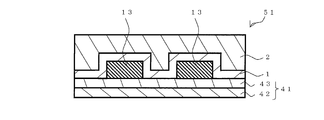
封止工程では、第1の樹脂層1が粘着シート41及び電子デバイス13と接触するように、粘着シート41上に樹脂シート11を積層し、電子デバイス13を樹脂シート11で封止する(図7参照)。これにより、電子デバイス13が樹脂封止された封止体51を得る。
封止工程では、第1の樹脂層1が粘着シート41及び電子デバイス13と接触するように、粘着シート41上に樹脂シート11を積層し、電子デバイス13を樹脂シート11で封止する(図7参照)。これにより、電子デバイス13が樹脂封止された封止体51を得る。
樹脂シート11を粘着シート41上に積層する方法は特に限定されず、熱プレスやラミネータなど公知の方法により行うことができる。
(熱硬化工程)
必要に応じて、封止体51を熱硬化する(封止体51の樹脂シート11を熱硬化する)。
必要に応じて、封止体51を熱硬化する(封止体51の樹脂シート11を熱硬化する)。
(剥離工程)
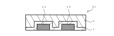
次いで、封止体51から粘着シート41を剥離する(図8参照)。剥離方法は特に限定されないが、粘着剤層43の粘着力を低下させた後に剥離することが好ましい。例えば、粘着剤層43が熱剥離性粘着剤層である場合、粘着剤層43を加熱し、粘着剤層43の粘着力を低下させた後に剥離する。
次いで、封止体51から粘着シート41を剥離する(図8参照)。剥離方法は特に限定されないが、粘着剤層43の粘着力を低下させた後に剥離することが好ましい。例えば、粘着剤層43が熱剥離性粘着剤層である場合、粘着剤層43を加熱し、粘着剤層43の粘着力を低下させた後に剥離する。
(研削工程)
次いで、必要に応じて、封止体51の樹脂シート11を研削する(図9参照)。研削方法としては、例えば、高速回転する砥石を用いるグラインディング法などが挙げられる。
次いで、必要に応じて、封止体51の樹脂シート11を研削する(図9参照)。研削方法としては、例えば、高速回転する砥石を用いるグラインディング法などが挙げられる。
(配線層形成工程)
次いで、セミアディティブ法などを利用して、封止体51に再配線52を形成する(図10参照)。
次いで、セミアディティブ法などを利用して、封止体51に再配線52を形成する(図10参照)。
その後、封止体51の再配線52を形成した面に、ポリイミドやポリベンゾオキサゾール(PBO)などの絶縁層を形成する。絶縁層は、例えば、ドライフィルムレジストなどのフィルムをラミネートすることで形成できる。
次いで、再配線52上にバンプ53を形成するバンピング加工を行う。バンピング加工は、半田ボールや半田メッキ等公知の方法で行うことができる。
(ダイシング工程)
電子デバイス13、第1の樹脂層1及び再配線52などの要素からなる封止体51のダイシングを行ってもよい(図11参照)。以上により、チップ領域の外側に配線を引き出した電子デバイスパッケージ61得ることができる。なお、ダイシングせずに封止体51をそのまま電子デバイスパッケージとして使用してもよい。
電子デバイス13、第1の樹脂層1及び再配線52などの要素からなる封止体51のダイシングを行ってもよい(図11参照)。以上により、チップ領域の外側に配線を引き出した電子デバイスパッケージ61得ることができる。なお、ダイシングせずに封止体51をそのまま電子デバイスパッケージとして使用してもよい。
(基板実装工程)
必要に応じて、電子デバイスパッケージ61を基板に実装する。
必要に応じて、電子デバイスパッケージ61を基板に実装する。
(レーザーマーキング工程)
レーザーマーキングは、封止体51又は電子デバイスパッケージ61に任意のタイミングで行うことができる。例えば、熱硬化前の封止体51にレーザーマーキングを行ってもよく、熱硬化後の封止体51にレーザーマーキングを行ってもよく、電子デバイスパッケージ61にレーザーマーキングを行ってもよい。
レーザーマーキングは、封止体51又は電子デバイスパッケージ61に任意のタイミングで行うことができる。例えば、熱硬化前の封止体51にレーザーマーキングを行ってもよく、熱硬化後の封止体51にレーザーマーキングを行ってもよく、電子デバイスパッケージ61にレーザーマーキングを行ってもよい。
電子デバイスパッケージ61において、高熱伝導率の第1の樹脂層1が電子デバイス13と接触しているので、電子デバイス13で発生した熱を、基板など(例えば、基板、筐体など)に逃がすことができる。したがって、ホットスポットを解消できる。なお、電子デバイス13で発生した熱は、第1の樹脂層1、再配線52及びバンプ53などを経由して、基板に伝わることができる。
電子デバイスパッケージ61は、パッケージオンパッケージ(PoP)、システムインパッケージ(SiP)、マルチチップパッケージ(MCP)などの実装方法に好適に適用できる。なお、パッケージオンパッケージ(PoP)では、スルーモールドビア(TMV)を採用することにより、熱を良好に逃がすことができる。
(変形例)
実施形態1では、第1の樹脂層1と、第1の樹脂層1上に配置された第2の樹脂層2とを備える樹脂シート11について説明した。変形例1では、樹脂シートは、第1の樹脂層1と、第1の樹脂層1上に配置された第3の層と、第3の層上に配置された第2の樹脂層2とを備える。変形例2では、樹脂シートは、第1の樹脂層1と、第1の樹脂層1上に配置された第2の樹脂層2と、第2の樹脂層2上に配置された第3の層とを備える。第3の層としては、例えば、樹脂を含む層、金属層などが好適である。第3の層は単層であってもよいし、複層であってもよい。
(変形例)
実施形態1では、第1の樹脂層1と、第1の樹脂層1上に配置された第2の樹脂層2とを備える樹脂シート11について説明した。変形例1では、樹脂シートは、第1の樹脂層1と、第1の樹脂層1上に配置された第3の層と、第3の層上に配置された第2の樹脂層2とを備える。変形例2では、樹脂シートは、第1の樹脂層1と、第1の樹脂層1上に配置された第2の樹脂層2と、第2の樹脂層2上に配置された第3の層とを備える。第3の層としては、例えば、樹脂を含む層、金属層などが好適である。第3の層は単層であってもよいし、複層であってもよい。
[実施形態2]
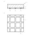
図12の(a)は実施形態2の樹脂シート101の断面模式図である。(b)はその模式底面図である。熱伝導粒子の含有量が少ない又は熱伝導粒子を含まない樹脂層31が、第1の樹脂層1のダイシングが予定されている部分(ダイシング予定部分)に形成されている点以外は、樹脂シート101は実施形態1の樹脂シート11と同様である。
図12の(a)は実施形態2の樹脂シート101の断面模式図である。(b)はその模式底面図である。熱伝導粒子の含有量が少ない又は熱伝導粒子を含まない樹脂層31が、第1の樹脂層1のダイシングが予定されている部分(ダイシング予定部分)に形成されている点以外は、樹脂シート101は実施形態1の樹脂シート11と同様である。
熱伝導粒子(特にアルミナ)は非常に硬く、ダイシングブレードの摩耗の原因となるが、樹脂シート101はダイシング予定部分に樹脂層31を備えるため、ダイシングブレードの摩耗を低減できる。また、第1の樹脂層1において、樹脂層31以外の部分は高熱伝導率であるため、電子デバイスの熱を基板に逃がすことができる。
樹脂層31中の熱伝導粒子の含有量は、30体積%以下であり、好ましくは0体積%である。30体積%以下であるので、ダイシングブレードの摩耗を低減できる。
樹脂層31は、エポキシ樹脂を含むことが好ましい。エポキシ樹脂としては、第1の樹脂層1で説明したものを好適に使用できる。
樹脂層31は、フェノール樹脂を含むことが好ましい。フェノール樹脂としては、第1の樹脂層1で説明したものを好適に使用できる。
エポキシ樹脂とフェノール樹脂の配合割合は、硬化反応性という観点から、エポキシ樹脂中のエポキシ基1当量に対して、フェノール樹脂中の水酸基の合計が0.7~1.5当量となるように配合することが好ましく、より好ましくは0.9~1.2当量である。
樹脂層31は、熱可塑性樹脂を含むことが好ましい。熱可塑性樹脂としては、第1の樹脂層1で説明したものを好適に使用できる。
樹脂層31は、フィラーを含むことが好ましい。フィラーとしては、第2の樹脂層2で説明したものを好適に使用できる。
樹脂層31は、硬化促進剤を含むことが好ましい。硬化促進剤としては、第1の樹脂層1で説明したものを好適に使用できる。
第1の樹脂層1のダイシング予定部分に樹脂層31を形成する方法は特に限定されず、例えば、第1の樹脂層1からダイシング予定部分の樹脂層を取り除いてスペースを設け、スペースに樹脂層31を形成するための溶液を充填し、乾燥させることで、樹脂層31を形成できる。
(変形例)
実施形態2では、第1の樹脂層1と、第1の樹脂層1上に配置された第2の樹脂層2とを備える樹脂シート101について説明した。変形例1では、樹脂シートは、第1の樹脂層1と、第1の樹脂層1上に配置された第3の層と、第3の層上に配置された第2の樹脂層2とを備える。変形例2では、樹脂シートは、第1の樹脂層1と、第1の樹脂層1上に配置された第2の樹脂層2と、第2の樹脂層2上に配置された第3の層とを備える。第3の層としては、例えば、樹脂を含む層、金属層などが好適である。第3の層は単層であってもよいし、複層であってもよい。
(変形例)
実施形態2では、第1の樹脂層1と、第1の樹脂層1上に配置された第2の樹脂層2とを備える樹脂シート101について説明した。変形例1では、樹脂シートは、第1の樹脂層1と、第1の樹脂層1上に配置された第3の層と、第3の層上に配置された第2の樹脂層2とを備える。変形例2では、樹脂シートは、第1の樹脂層1と、第1の樹脂層1上に配置された第2の樹脂層2と、第2の樹脂層2上に配置された第3の層とを備える。第3の層としては、例えば、樹脂を含む層、金属層などが好適である。第3の層は単層であってもよいし、複層であってもよい。
以下に、この発明の好適な実施例を例示的に詳しく説明する。ただし、この実施例に記載されている材料や配合量などは、特に限定的な記載がない限りは、この発明の範囲をそれらのみに限定する趣旨のものではない。
まず、実施例で使用した成分について説明する。
第1の樹脂層を作製するために使用した成分について説明する。
エポキシ樹脂:新日鐵化学(株)製のYSLV-80XY(ビスフェノールF型エポキシ樹脂、エポキン当量200g/eq.軟化点80℃)
フェノール樹脂:明和化成社製のMEH-7851-SS(ビフェニルアラルキル骨格を有するフェノール樹脂、水酸基当量203g/eq.軟化点67℃)
熱可塑性樹脂:三菱レイヨン社製メタブレンC-132E(MBS樹脂、平均粒径120μm)
熱伝導粒子:電気化学工業製のDAB-45SI(アルミナ、d50 19.9μm、熱伝導率30W/mK)
難燃剤:伏見製薬所製のFP-100(ホスファゼン化合物)
硬化促進剤:四国化成工業社製の2PHZ-PW(2-フェニル-4,5-ジヒドロキシメチルイミダゾール)
エポキシ樹脂:新日鐵化学(株)製のYSLV-80XY(ビスフェノールF型エポキシ樹脂、エポキン当量200g/eq.軟化点80℃)
フェノール樹脂:明和化成社製のMEH-7851-SS(ビフェニルアラルキル骨格を有するフェノール樹脂、水酸基当量203g/eq.軟化点67℃)
熱可塑性樹脂:三菱レイヨン社製メタブレンC-132E(MBS樹脂、平均粒径120μm)
熱伝導粒子:電気化学工業製のDAB-45SI(アルミナ、d50 19.9μm、熱伝導率30W/mK)
難燃剤:伏見製薬所製のFP-100(ホスファゼン化合物)
硬化促進剤:四国化成工業社製の2PHZ-PW(2-フェニル-4,5-ジヒドロキシメチルイミダゾール)
第2の樹脂層を作製するために使用した成分について説明する。
エポキシ樹脂:新日鐵化学(株)製のYSLV-80XY(ビスフェノールF型エポキシ樹脂、エポキン当量200g/eq.軟化点80℃)
フェノール樹脂:明和化成社製のMEH-7851-SS(ビフェニルアラルキル骨格を有するフェノール樹脂、水酸基当量203g/eq.軟化点67℃)
熱可塑性樹脂:三菱レイヨン社製メタブレンC-132E(MBS樹脂、平均粒径120μm)
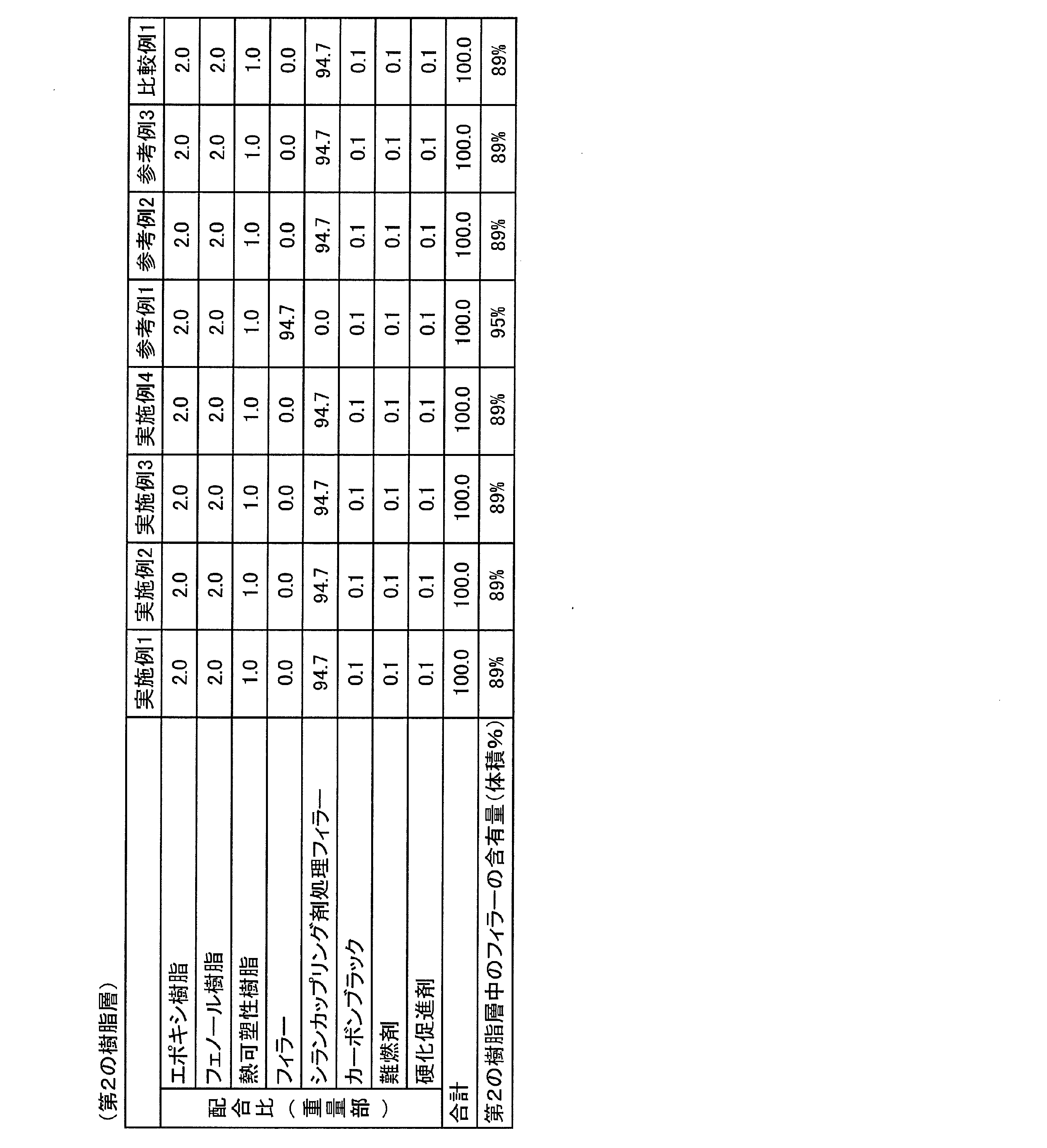
フィラー:電気化学工業社製のFB-9454FC(溶融球状シリカ、平均粒子径20μm)
シランカップリング剤:信越化学社製のKBM-403(3-グリシドキシプロピルトリメトキシシラン)
シランカップリング剤処理フィラー:電気化学工業社製のFB-9454FC(溶融球状シリカ、平均一次粒子径20μm)を信越化学社製のKBM-403(3-グリシドキシプロピルトリメトキシシラン)で処理したもの(FB-9454FC 87.9重量部に対して、KBM-403 0.5重量部の割合で処理)
カーボンブラック:三菱化学社製の#20
難燃剤:伏見製薬所製のFP-100(ホスファゼン化合物)
硬化促進剤:四国化成工業社製の2PHZ-PW(2-フェニル-4,5-ジヒドロキシメチルイミダゾール)
エポキシ樹脂:新日鐵化学(株)製のYSLV-80XY(ビスフェノールF型エポキシ樹脂、エポキン当量200g/eq.軟化点80℃)
フェノール樹脂:明和化成社製のMEH-7851-SS(ビフェニルアラルキル骨格を有するフェノール樹脂、水酸基当量203g/eq.軟化点67℃)
熱可塑性樹脂:三菱レイヨン社製メタブレンC-132E(MBS樹脂、平均粒径120μm)
フィラー:電気化学工業社製のFB-9454FC(溶融球状シリカ、平均粒子径20μm)
シランカップリング剤:信越化学社製のKBM-403(3-グリシドキシプロピルトリメトキシシラン)
シランカップリング剤処理フィラー:電気化学工業社製のFB-9454FC(溶融球状シリカ、平均一次粒子径20μm)を信越化学社製のKBM-403(3-グリシドキシプロピルトリメトキシシラン)で処理したもの(FB-9454FC 87.9重量部に対して、KBM-403 0.5重量部の割合で処理)
カーボンブラック:三菱化学社製の#20
難燃剤:伏見製薬所製のFP-100(ホスファゼン化合物)
硬化促進剤:四国化成工業社製の2PHZ-PW(2-フェニル-4,5-ジヒドロキシメチルイミダゾール)
[実施例、参考例及び比較例]
(第1の樹脂層の作製)
表1に記載の配合比に従い、各成分を配合し、これに各成分の総量と同量のメチルエチルケトンを添加して、ワニスを調製した。得られたワニスを、コンマコ―タ-により、厚み50μmのポリエステルフィルムA(三菱化学ポリエステル社製、MRF-50)の剥離処理面上に塗工し、乾燥させた。次いで、厚み38μmのポリエステルフィルムB(三菱化学ポリエステル社製、MRF-38)の剥離処理面を、乾燥後のワニス上に張り合わせて、第1の樹脂層を作製した(第1の樹脂層の厚み 70μm)。
(第1の樹脂層の作製)
表1に記載の配合比に従い、各成分を配合し、これに各成分の総量と同量のメチルエチルケトンを添加して、ワニスを調製した。得られたワニスを、コンマコ―タ-により、厚み50μmのポリエステルフィルムA(三菱化学ポリエステル社製、MRF-50)の剥離処理面上に塗工し、乾燥させた。次いで、厚み38μmのポリエステルフィルムB(三菱化学ポリエステル社製、MRF-38)の剥離処理面を、乾燥後のワニス上に張り合わせて、第1の樹脂層を作製した(第1の樹脂層の厚み 70μm)。
表3に記載の熱伝導粒子量である点以外は、第1の樹脂層と同様のワニスを調製した。第1の樹脂層からダイシング予定部分の樹脂層を取り除いてスペースを設けた後、スペースにワニスを充填し、これを乾燥させることで、第1の樹脂層のダイシング予定部分に樹脂層を形成した。
すなわち、第1の樹脂層において、ダイシング予定部分の樹脂層と、ダイシング予定部分以外の樹脂層とは、熱伝導粒子量のみが異なる。

(第2の樹脂層の作製)
表2に記載の配合比に従い、各成分を配合し、ロール混練機により60~120℃、10分間、減圧条件下(0.01kg/cm2)で溶融混練し、混練物を調製した。次いで、得られた混練物を、平板プレス法により、シート状に形成して、第2の樹脂層を作製した(第2の樹脂層の厚み 130μm)。
表2に記載の配合比に従い、各成分を配合し、ロール混練機により60~120℃、10分間、減圧条件下(0.01kg/cm2)で溶融混練し、混練物を調製した。次いで、得られた混練物を、平板プレス法により、シート状に形成して、第2の樹脂層を作製した(第2の樹脂層の厚み 130μm)。
(樹脂シートの作製)
第1の樹脂層のポリエステルフィルムAを剥離した後、ロールラミネ―タ―を用いて第2の樹脂層上に第1の樹脂層を積層した。これにより、第2の樹脂層上に第1の樹脂層が積層された樹脂シートを作製した。
第1の樹脂層のポリエステルフィルムAを剥離した後、ロールラミネ―タ―を用いて第2の樹脂層上に第1の樹脂層を積層した。これにより、第2の樹脂層上に第1の樹脂層が積層された樹脂シートを作製した。
(評価)
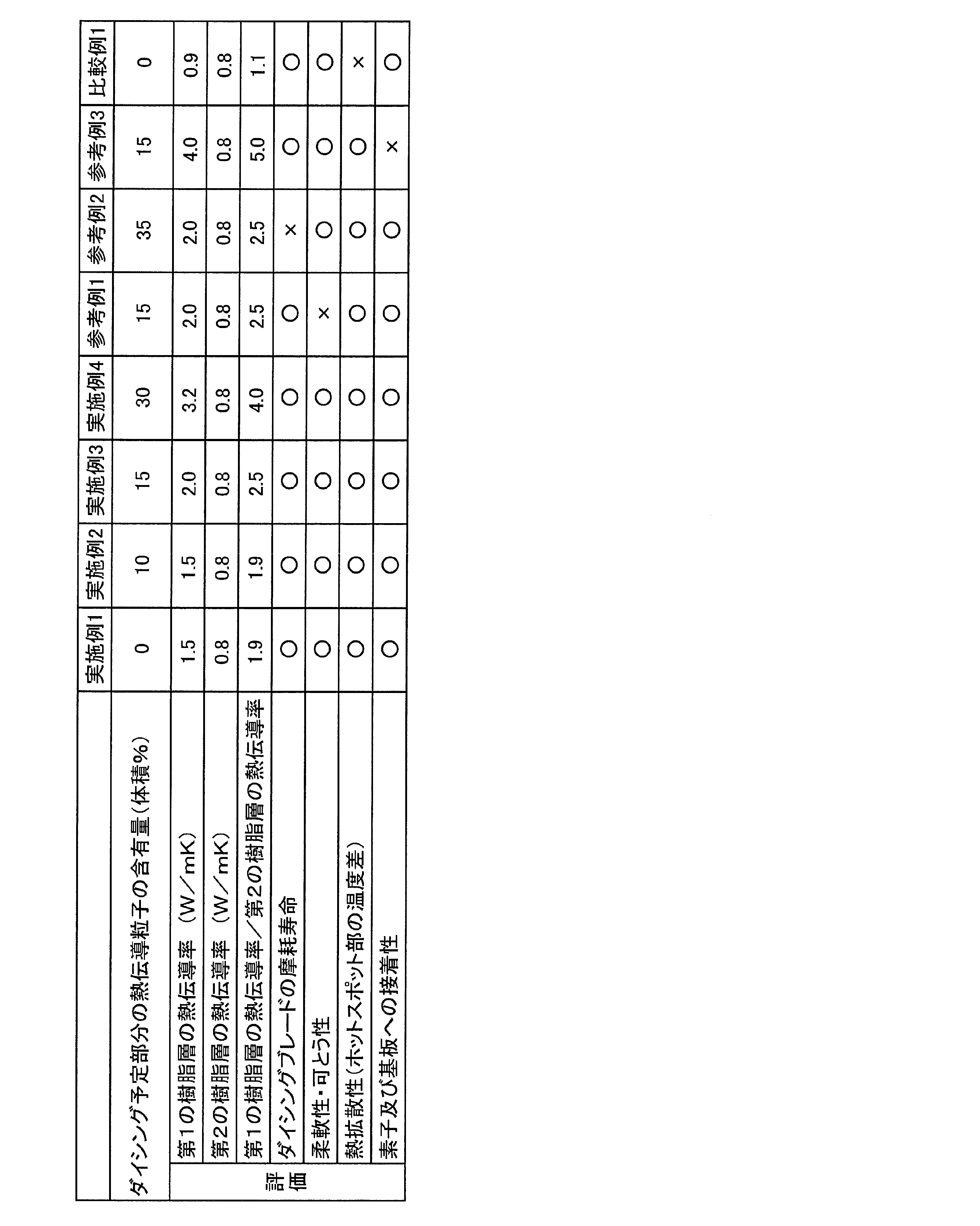
第1の樹脂層、第2の樹脂層及び樹脂シートについて以下の評価を行った。結果を表3に示す。
第1の樹脂層、第2の樹脂層及び樹脂シートについて以下の評価を行った。結果を表3に示す。
(熱伝導率)
サンプル(第1の樹脂層及び第2の樹脂層)を、乾燥機内において175℃、1時間で熱処理を行い、熱硬化させた。その後、TWA法(温度波熱分析法、測定装置;アイフェイズモバイル、(株)アイフェイズ製)により、サンプルの熱拡散率α(m2/s)を測定した。次に、サンプルの比熱Cp(J/g・℃)を、DSC法により測定した。比熱測定は、エスアイアイナノテクノロジー(株)製のDSC6220を用い、昇温速度10℃/min、温度20~300℃の条件下で行い、得られた実験データを基に、JISハンドブック(比熱容量測定方法K-7123)により算出した。更に、サンプルの比重を測定した。
サンプル(第1の樹脂層及び第2の樹脂層)を、乾燥機内において175℃、1時間で熱処理を行い、熱硬化させた。その後、TWA法(温度波熱分析法、測定装置;アイフェイズモバイル、(株)アイフェイズ製)により、サンプルの熱拡散率α(m2/s)を測定した。次に、サンプルの比熱Cp(J/g・℃)を、DSC法により測定した。比熱測定は、エスアイアイナノテクノロジー(株)製のDSC6220を用い、昇温速度10℃/min、温度20~300℃の条件下で行い、得られた実験データを基に、JISハンドブック(比熱容量測定方法K-7123)により算出した。更に、サンプルの比重を測定した。
熱拡散率α、比熱Cp及び比重の値を基に、下記式により熱伝導率を算出した。

[ダイシングブレードの摩耗寿命]
SAWフィルタ(チップ厚み200μm、バンプ高さ20μm)がマトリックス状に配列されたセラミック基板上に樹脂シートを積層し、温度100℃,圧力300kPaの条件にて1分間真空プレス(到達真空度6.65×10² Pa)した。大気開放後、SAWフィルタパッケージを130℃のオーブンに3時間投入することにより樹脂シートを硬化させた。その後、ダイシング装置を用いてSAWフィルタパッケージを個片化した。ダイシング後に、ダイシング装置(DFD6361、DISCO社製)の接触式のブレード位置合わせ機能で、ダイシングブレードの摩耗量を測定して求めた。摩耗量が30μm未満である場合を○、摩耗量が30μm以上である場合を×と判定した。
SAWフィルタ(チップ厚み200μm、バンプ高さ20μm)がマトリックス状に配列されたセラミック基板上に樹脂シートを積層し、温度100℃,圧力300kPaの条件にて1分間真空プレス(到達真空度6.65×10² Pa)した。大気開放後、SAWフィルタパッケージを130℃のオーブンに3時間投入することにより樹脂シートを硬化させた。その後、ダイシング装置を用いてSAWフィルタパッケージを個片化した。ダイシング後に、ダイシング装置(DFD6361、DISCO社製)の接触式のブレード位置合わせ機能で、ダイシングブレードの摩耗量を測定して求めた。摩耗量が30μm未満である場合を○、摩耗量が30μm以上である場合を×と判定した。
[柔軟性・可とう性]
温度25℃において直径30mmのステンレス製パイプに樹脂シートを巻きつけた際、樹脂シートに割れ(クラック)が発生した場合を×、割れ(クラック)が発生しない場合を○と判定した。
温度25℃において直径30mmのステンレス製パイプに樹脂シートを巻きつけた際、樹脂シートに割れ(クラック)が発生した場合を×、割れ(クラック)が発生しない場合を○と判定した。
[熱拡散性(ホットスポット面積)]
SAWフィルタ(チップ厚み200μm、バンプ高さ20μm)がマトリックス状に配列されたセラミック基板上に樹脂シートを積層し、温度100℃,圧力300kPaの条件にて1分間真空プレス(到達真空度6.65×10² Pa)した。大気開放後、SAWフィルタパッケージを130℃のオーブンに3時間投入することにより樹脂シートを硬化させた。その後、ダイシング装置を用いてSAWフィルタパッケージを個片化した。
個片化したSAWフィルタを、SAWフィルタ試験装置を用いて駆動試験を行った。駆動中のSAWフィルタを赤外線サーモグラフィを用いてSAWフィルタ表面の温度分布(ホットスポット)を測定した。そして、ホットスポット部の温度がパッケージ表面の最低温度部より +10℃未満である場合を○、ホットスポット面積が +10℃以上である場合を×と判定した。
SAWフィルタ(チップ厚み200μm、バンプ高さ20μm)がマトリックス状に配列されたセラミック基板上に樹脂シートを積層し、温度100℃,圧力300kPaの条件にて1分間真空プレス(到達真空度6.65×10² Pa)した。大気開放後、SAWフィルタパッケージを130℃のオーブンに3時間投入することにより樹脂シートを硬化させた。その後、ダイシング装置を用いてSAWフィルタパッケージを個片化した。
個片化したSAWフィルタを、SAWフィルタ試験装置を用いて駆動試験を行った。駆動中のSAWフィルタを赤外線サーモグラフィを用いてSAWフィルタ表面の温度分布(ホットスポット)を測定した。そして、ホットスポット部の温度がパッケージ表面の最低温度部より +10℃未満である場合を○、ホットスポット面積が +10℃以上である場合を×と判定した。
[素子及び基板への接着性]
素子を5mm×5mmの個片に切断し、その個片を樹脂シート表面に配置し、温度100℃,圧力300kPaの条件にて1分間真空プレス(到達真空度6.65×10² Pa)した。その後、130℃のオーブンに3時間投入することにより樹脂シートを硬化させた。硬化後、Dage社製万能型ボンドテスター(Dage4000)を用い、素子のせん断接着力を測定した。
基板を5mm×5mmの個片に切断し、その個片を樹脂シート表面に配置し、温度100℃,圧力300kPaの条件にて1分間真空プレス(到達真空度6.65×10² Pa)した。その後、130℃のオーブンに3時間投入することにより樹脂シートを硬化させた。硬化後、Dage社製万能型ボンドテスター(Dage4000)を用い、基板のせん断接着力を測定した。
素子のせん断接着力が8MPa以上であり、かつ基板のせん断接着力が8MPa以上である場合を○と判定した。素子のせん断接着力又は基板のせん断接着力が8MPa未満である場合を×と判定した。
素子を5mm×5mmの個片に切断し、その個片を樹脂シート表面に配置し、温度100℃,圧力300kPaの条件にて1分間真空プレス(到達真空度6.65×10² Pa)した。その後、130℃のオーブンに3時間投入することにより樹脂シートを硬化させた。硬化後、Dage社製万能型ボンドテスター(Dage4000)を用い、素子のせん断接着力を測定した。
基板を5mm×5mmの個片に切断し、その個片を樹脂シート表面に配置し、温度100℃,圧力300kPaの条件にて1分間真空プレス(到達真空度6.65×10² Pa)した。その後、130℃のオーブンに3時間投入することにより樹脂シートを硬化させた。硬化後、Dage社製万能型ボンドテスター(Dage4000)を用い、基板のせん断接着力を測定した。
素子のせん断接着力が8MPa以上であり、かつ基板のせん断接着力が8MPa以上である場合を○と判定した。素子のせん断接着力又は基板のせん断接着力が8MPa未満である場合を×と判定した。
1 第1の樹脂層
2 第2の樹脂層
11 樹脂シート
12 基板
13 電子デバイス
13a 突起電極
14 中空部
15、16 電子デバイスパッケージ
17 バンプ
18 基板
41 粘着シート
42 支持体
43 粘着剤層
51 封止体
52 再配線
53 バンプ
61 電子デバイスパッケージ
101 樹脂シート
2 第2の樹脂層
11 樹脂シート
12 基板
13 電子デバイス
13a 突起電極
14 中空部
15、16 電子デバイスパッケージ
17 バンプ
18 基板
41 粘着シート
42 支持体
43 粘着剤層
51 封止体
52 再配線
53 バンプ
61 電子デバイスパッケージ
101 樹脂シート
Claims (5)
- 第1の樹脂層及び第2の樹脂層を備え、
前記第1の樹脂層の熱伝導率が1W/mK以上である電子デバイス封止用樹脂シート。 - 前記第1の樹脂層は熱伝導粒子を含み、
前記第1の樹脂層中の前記熱伝導粒子の含有量が55~83体積%である請求項1に記載の電子デバイス封止用樹脂シート。 - 前記熱伝導粒子がアルミナ及び/又は窒化ホウ素である請求項1又は2に記載の電子デバイス封止用樹脂シート。
- 前記熱伝導粒子の含有量が30体積%以下の樹脂層が、前記第1の樹脂層のダイシングが予定されている部分に形成されている請求項1~3のいずれかに記載の電子デバイス封止用樹脂シート。
- 前記第1の樹脂層が電子デバイスと接触するように、請求項1~4のいずれかに記載の電子デバイス封止用樹脂シートで前記電子デバイスを封止する工程を含む電子デバイスパッケージの製造方法。
Priority Applications (2)
| Application Number | Priority Date | Filing Date | Title |
|---|---|---|---|
| SG11201600906YA SG11201600906YA (en) | 2013-08-09 | 2014-07-04 | Resin sheet for electronic device encapsulation and method for manufacturing electronic device package |
| CN201480043548.2A CN105453252B (zh) | 2013-08-09 | 2014-07-04 | 电子器件密封用树脂片及电子器件封装件的制造方法 |
Applications Claiming Priority (2)
| Application Number | Priority Date | Filing Date | Title |
|---|---|---|---|
| JP2013-167055 | 2013-08-09 | ||
| JP2013167055A JP6259608B2 (ja) | 2013-08-09 | 2013-08-09 | 電子デバイス封止用樹脂シート及び電子デバイスパッケージの製造方法 |
Publications (1)
| Publication Number | Publication Date |
|---|---|
| WO2015019769A1 true WO2015019769A1 (ja) | 2015-02-12 |
Family
ID=52461108
Family Applications (1)
| Application Number | Title | Priority Date | Filing Date |
|---|---|---|---|
| PCT/JP2014/067921 Ceased WO2015019769A1 (ja) | 2013-08-09 | 2014-07-04 | 電子デバイス封止用樹脂シート及び電子デバイスパッケージの製造方法 |
Country Status (5)
| Country | Link |
|---|---|
| JP (1) | JP6259608B2 (ja) |
| CN (1) | CN105453252B (ja) |
| SG (1) | SG11201600906YA (ja) |
| TW (1) | TW201513278A (ja) |
| WO (1) | WO2015019769A1 (ja) |
Cited By (2)
| Publication number | Priority date | Publication date | Assignee | Title |
|---|---|---|---|---|
| JP2017117842A (ja) * | 2015-12-21 | 2017-06-29 | 京セラ株式会社 | 電子部品及び電子部品の製造方法 |
| CN116134066A (zh) * | 2020-07-21 | 2023-05-16 | 京瓷株式会社 | 导热性粘合用片和半导体装置 |
Families Citing this family (13)
| Publication number | Priority date | Publication date | Assignee | Title |
|---|---|---|---|---|
| US9761540B2 (en) | 2015-06-24 | 2017-09-12 | Micron Technology, Inc. | Wafer level package and fabrication method thereof |
| JP6461031B2 (ja) * | 2016-03-16 | 2019-01-30 | 東芝メモリ株式会社 | 半導体装置の製造方法 |
| JP2018051892A (ja) * | 2016-09-28 | 2018-04-05 | 京セラ株式会社 | 熱硬化性樹脂シート、その製造方法および電子部品の封止方法 |
| CN106684057B (zh) * | 2016-12-30 | 2019-10-22 | 华为技术有限公司 | 芯片封装结构及其制造方法 |
| JP6975547B2 (ja) * | 2017-03-31 | 2021-12-01 | ナガセケムテックス株式会社 | 実装構造体の製造方法およびこれに用いられる積層シート |
| JP6894076B2 (ja) * | 2017-03-31 | 2021-06-23 | ナガセケムテックス株式会社 | 実装構造体の製造方法およびこれに用いられる積層シート |
| TWI645523B (zh) * | 2017-07-14 | 2018-12-21 | 矽品精密工業股份有限公司 | 封裝結構及其製法 |
| CN110914977A (zh) | 2017-07-21 | 2020-03-24 | 株式会社村田制作所 | 电子部件 |
| JP7038726B2 (ja) * | 2017-09-29 | 2022-03-18 | ナガセケムテックス株式会社 | 実装構造体の製造方法およびこれに用いられるシート |
| KR102522785B1 (ko) | 2017-09-29 | 2023-04-18 | 나가세케무텍쿠스가부시키가이샤 | 실장 구조체의 제조 방법 및 이것에 이용되는 적층 시트 |
| JP7119817B2 (ja) * | 2018-09-18 | 2022-08-17 | 昭和電工マテリアルズ株式会社 | 半導体装置 |
| JPWO2020241505A1 (ja) * | 2019-05-31 | 2020-12-03 | ||
| WO2022024369A1 (ja) * | 2020-07-31 | 2022-02-03 | 国立大学法人東北大学 | 半導体装置の製造方法、半導体装置を備えた装置の製造方法、半導体装置、半導体装置を備えた装置 |
Citations (4)
| Publication number | Priority date | Publication date | Assignee | Title |
|---|---|---|---|---|
| JP2008288433A (ja) * | 2007-05-18 | 2008-11-27 | Yaskawa Electric Corp | 実装基板の樹脂モールド方法とその装置および樹脂モールド実装基板 |
| JP2010109246A (ja) * | 2008-10-31 | 2010-05-13 | Yaskawa Electric Corp | 半導体装置および半導体装置の製造方法 |
| US20100219524A1 (en) * | 2009-02-27 | 2010-09-02 | Chi-Chih Shen | Chip scale package and method of fabricating the same |
| JP2013004848A (ja) * | 2011-06-20 | 2013-01-07 | Semiconductor Components Industries Llc | 半導体装置およびその製造方法 |
Family Cites Families (3)
| Publication number | Priority date | Publication date | Assignee | Title |
|---|---|---|---|---|
| JPH11310766A (ja) * | 1998-04-28 | 1999-11-09 | Hitachi Chem Co Ltd | 封止用エポキシ樹脂成形材料及び電子部品装置 |
| JP2011054806A (ja) * | 2009-09-02 | 2011-03-17 | Renesas Electronics Corp | 半導体装置およびその製造方法 |
| JP2011216849A (ja) * | 2010-03-17 | 2011-10-27 | Tdk Corp | 電子回路モジュール部品及び電子回路モジュール部品の製造方法 |
-
2013
- 2013-08-09 JP JP2013167055A patent/JP6259608B2/ja active Active
-
2014
- 2014-07-04 CN CN201480043548.2A patent/CN105453252B/zh not_active Expired - Fee Related
- 2014-07-04 WO PCT/JP2014/067921 patent/WO2015019769A1/ja not_active Ceased
- 2014-07-04 SG SG11201600906YA patent/SG11201600906YA/en unknown
- 2014-07-09 TW TW103123613A patent/TW201513278A/zh unknown
Patent Citations (4)
| Publication number | Priority date | Publication date | Assignee | Title |
|---|---|---|---|---|
| JP2008288433A (ja) * | 2007-05-18 | 2008-11-27 | Yaskawa Electric Corp | 実装基板の樹脂モールド方法とその装置および樹脂モールド実装基板 |
| JP2010109246A (ja) * | 2008-10-31 | 2010-05-13 | Yaskawa Electric Corp | 半導体装置および半導体装置の製造方法 |
| US20100219524A1 (en) * | 2009-02-27 | 2010-09-02 | Chi-Chih Shen | Chip scale package and method of fabricating the same |
| JP2013004848A (ja) * | 2011-06-20 | 2013-01-07 | Semiconductor Components Industries Llc | 半導体装置およびその製造方法 |
Cited By (3)
| Publication number | Priority date | Publication date | Assignee | Title |
|---|---|---|---|---|
| JP2017117842A (ja) * | 2015-12-21 | 2017-06-29 | 京セラ株式会社 | 電子部品及び電子部品の製造方法 |
| CN116134066A (zh) * | 2020-07-21 | 2023-05-16 | 京瓷株式会社 | 导热性粘合用片和半导体装置 |
| EP4186937A4 (en) * | 2020-07-21 | 2024-08-07 | Kyocera Corporation | Thermally conductive adhesive sheet and semiconductor device |
Also Published As
| Publication number | Publication date |
|---|---|
| SG11201600906YA (en) | 2016-03-30 |
| CN105453252A (zh) | 2016-03-30 |
| JP2015035567A (ja) | 2015-02-19 |
| CN105453252B (zh) | 2018-10-26 |
| JP6259608B2 (ja) | 2018-01-10 |
| TW201513278A (zh) | 2015-04-01 |
Similar Documents
| Publication | Publication Date | Title |
|---|---|---|
| JP6259608B2 (ja) | 電子デバイス封止用樹脂シート及び電子デバイスパッケージの製造方法 | |
| JP6320239B2 (ja) | 半導体チップ封止用熱硬化性樹脂シート及び半導体パッケージの製造方法 | |
| JP6356395B2 (ja) | 電子デバイス封止用樹脂シート及び電子デバイスパッケージの製造方法 | |
| JP6393092B2 (ja) | 中空型電子デバイス封止用樹脂シート及び中空型電子デバイスパッケージの製造方法 | |
| WO2015098833A1 (ja) | 半導体パッケージの製造方法 | |
| WO2014156837A1 (ja) | 中空封止用樹脂シート及び中空パッケージの製造方法 | |
| US20170125373A1 (en) | Method for producing semiconductor package | |
| WO2015098829A1 (ja) | 半導体パッケージの製造方法 | |
| JP5793160B2 (ja) | 電子デバイス封止用樹脂シート及び電子デバイスパッケージの製造方法 | |
| WO2015098838A1 (ja) | 半導体装置の製造方法及び熱硬化性樹脂シート | |
| WO2016072236A1 (ja) | 樹脂組成物、半導体装置の製造方法及び半導体装置 | |
| WO2014156833A1 (ja) | 中空封止用樹脂シート及び中空パッケージの製造方法 | |
| WO2014156777A1 (ja) | 中空型電子デバイス封止用シート、及び、中空型電子デバイスパッケージの製造方法 | |
| JP5735030B2 (ja) | 電子デバイス封止用樹脂シート及び電子デバイスパッケージの製造方法 | |
| WO2016080117A1 (ja) | セパレータ付き封止用シート、及び、半導体装置の製造方法 | |
| JP6302692B2 (ja) | 中空封止用樹脂シート及び中空パッケージの製造方法 |
Legal Events
| Date | Code | Title | Description |
|---|---|---|---|
| WWE | Wipo information: entry into national phase |
Ref document number: 201480043548.2 Country of ref document: CN |
|
| 121 | Ep: the epo has been informed by wipo that ep was designated in this application |
Ref document number: 14835063 Country of ref document: EP Kind code of ref document: A1 |
|
| NENP | Non-entry into the national phase |
Ref country code: DE |
|
| 122 | Ep: pct application non-entry in european phase |
Ref document number: 14835063 Country of ref document: EP Kind code of ref document: A1 |