WO2015016196A1 - 表示装置およびその駆動方法 - Google Patents
表示装置およびその駆動方法 Download PDFInfo
- Publication number
- WO2015016196A1 WO2015016196A1 PCT/JP2014/069876 JP2014069876W WO2015016196A1 WO 2015016196 A1 WO2015016196 A1 WO 2015016196A1 JP 2014069876 W JP2014069876 W JP 2014069876W WO 2015016196 A1 WO2015016196 A1 WO 2015016196A1
- Authority
- WO
- WIPO (PCT)
- Prior art keywords
- noise
- characteristic detection
- characteristic
- period
- detected
- Prior art date
- Legal status (The legal status is an assumption and is not a legal conclusion. Google has not performed a legal analysis and makes no representation as to the accuracy of the status listed.)
- Ceased
Links
Images






















Classifications
-
- G—PHYSICS
- G09—EDUCATION; CRYPTOGRAPHY; DISPLAY; ADVERTISING; SEALS
- G09G—ARRANGEMENTS OR CIRCUITS FOR CONTROL OF INDICATING DEVICES USING STATIC MEANS TO PRESENT VARIABLE INFORMATION
- G09G3/00—Control arrangements or circuits, of interest only in connection with visual indicators other than cathode-ray tubes
- G09G3/20—Control arrangements or circuits, of interest only in connection with visual indicators other than cathode-ray tubes for presentation of an assembly of a number of characters, e.g. a page, by composing the assembly by combination of individual elements arranged in a matrix no fixed position being assigned to or needed to be assigned to the individual characters or partial characters
- G09G3/22—Control arrangements or circuits, of interest only in connection with visual indicators other than cathode-ray tubes for presentation of an assembly of a number of characters, e.g. a page, by composing the assembly by combination of individual elements arranged in a matrix no fixed position being assigned to or needed to be assigned to the individual characters or partial characters using controlled light sources
- G09G3/30—Control arrangements or circuits, of interest only in connection with visual indicators other than cathode-ray tubes for presentation of an assembly of a number of characters, e.g. a page, by composing the assembly by combination of individual elements arranged in a matrix no fixed position being assigned to or needed to be assigned to the individual characters or partial characters using controlled light sources using electroluminescent panels
- G09G3/32—Control arrangements or circuits, of interest only in connection with visual indicators other than cathode-ray tubes for presentation of an assembly of a number of characters, e.g. a page, by composing the assembly by combination of individual elements arranged in a matrix no fixed position being assigned to or needed to be assigned to the individual characters or partial characters using controlled light sources using electroluminescent panels semiconductive, e.g. using light-emitting diodes [LED]
- G09G3/3208—Control arrangements or circuits, of interest only in connection with visual indicators other than cathode-ray tubes for presentation of an assembly of a number of characters, e.g. a page, by composing the assembly by combination of individual elements arranged in a matrix no fixed position being assigned to or needed to be assigned to the individual characters or partial characters using controlled light sources using electroluminescent panels semiconductive, e.g. using light-emitting diodes [LED] organic, e.g. using organic light-emitting diodes [OLED]
- G09G3/3225—Control arrangements or circuits, of interest only in connection with visual indicators other than cathode-ray tubes for presentation of an assembly of a number of characters, e.g. a page, by composing the assembly by combination of individual elements arranged in a matrix no fixed position being assigned to or needed to be assigned to the individual characters or partial characters using controlled light sources using electroluminescent panels semiconductive, e.g. using light-emitting diodes [LED] organic, e.g. using organic light-emitting diodes [OLED] using an active matrix
- G09G3/3233—Control arrangements or circuits, of interest only in connection with visual indicators other than cathode-ray tubes for presentation of an assembly of a number of characters, e.g. a page, by composing the assembly by combination of individual elements arranged in a matrix no fixed position being assigned to or needed to be assigned to the individual characters or partial characters using controlled light sources using electroluminescent panels semiconductive, e.g. using light-emitting diodes [LED] organic, e.g. using organic light-emitting diodes [OLED] using an active matrix with pixel circuitry controlling the current through the light-emitting element
-
- G—PHYSICS
- G09—EDUCATION; CRYPTOGRAPHY; DISPLAY; ADVERTISING; SEALS
- G09G—ARRANGEMENTS OR CIRCUITS FOR CONTROL OF INDICATING DEVICES USING STATIC MEANS TO PRESENT VARIABLE INFORMATION
- G09G3/00—Control arrangements or circuits, of interest only in connection with visual indicators other than cathode-ray tubes
- G09G3/006—Electronic inspection or testing of displays and display drivers, e.g. of LED or LCD displays
-
- G—PHYSICS
- G09—EDUCATION; CRYPTOGRAPHY; DISPLAY; ADVERTISING; SEALS
- G09G—ARRANGEMENTS OR CIRCUITS FOR CONTROL OF INDICATING DEVICES USING STATIC MEANS TO PRESENT VARIABLE INFORMATION
- G09G2300/00—Aspects of the constitution of display devices
- G09G2300/04—Structural and physical details of display devices
- G09G2300/0404—Matrix technologies
-
- G—PHYSICS
- G09—EDUCATION; CRYPTOGRAPHY; DISPLAY; ADVERTISING; SEALS
- G09G—ARRANGEMENTS OR CIRCUITS FOR CONTROL OF INDICATING DEVICES USING STATIC MEANS TO PRESENT VARIABLE INFORMATION
- G09G2300/00—Aspects of the constitution of display devices
- G09G2300/08—Active matrix structure, i.e. with use of active elements, inclusive of non-linear two terminal elements, in the pixels together with light emitting or modulating elements
- G09G2300/0809—Several active elements per pixel in active matrix panels
- G09G2300/0842—Several active elements per pixel in active matrix panels forming a memory circuit, e.g. a dynamic memory with one capacitor
-
- G—PHYSICS
- G09—EDUCATION; CRYPTOGRAPHY; DISPLAY; ADVERTISING; SEALS
- G09G—ARRANGEMENTS OR CIRCUITS FOR CONTROL OF INDICATING DEVICES USING STATIC MEANS TO PRESENT VARIABLE INFORMATION
- G09G2310/00—Command of the display device
- G09G2310/02—Addressing, scanning or driving the display screen or processing steps related thereto
- G09G2310/0202—Addressing of scan or signal lines
- G09G2310/0205—Simultaneous scanning of several lines in flat panels
- G09G2310/021—Double addressing, i.e. scanning two or more lines, e.g. lines 2 and 3; 4 and 5, at a time in a first field, followed by scanning two or more lines in another combination, e.g. lines 1 and 2; 3 and 4, in a second field
-
- G—PHYSICS
- G09—EDUCATION; CRYPTOGRAPHY; DISPLAY; ADVERTISING; SEALS
- G09G—ARRANGEMENTS OR CIRCUITS FOR CONTROL OF INDICATING DEVICES USING STATIC MEANS TO PRESENT VARIABLE INFORMATION
- G09G2310/00—Command of the display device
- G09G2310/02—Addressing, scanning or driving the display screen or processing steps related thereto
- G09G2310/0202—Addressing of scan or signal lines
- G09G2310/0218—Addressing of scan or signal lines with collection of electrodes in groups for n-dimensional addressing
-
- G—PHYSICS
- G09—EDUCATION; CRYPTOGRAPHY; DISPLAY; ADVERTISING; SEALS
- G09G—ARRANGEMENTS OR CIRCUITS FOR CONTROL OF INDICATING DEVICES USING STATIC MEANS TO PRESENT VARIABLE INFORMATION
- G09G2310/00—Command of the display device
- G09G2310/08—Details of timing specific for flat panels, other than clock recovery
-
- G—PHYSICS
- G09—EDUCATION; CRYPTOGRAPHY; DISPLAY; ADVERTISING; SEALS
- G09G—ARRANGEMENTS OR CIRCUITS FOR CONTROL OF INDICATING DEVICES USING STATIC MEANS TO PRESENT VARIABLE INFORMATION
- G09G2320/00—Control of display operating conditions
- G09G2320/02—Improving the quality of display appearance
- G09G2320/029—Improving the quality of display appearance by monitoring one or more pixels in the display panel, e.g. by monitoring a fixed reference pixel
- G09G2320/0295—Improving the quality of display appearance by monitoring one or more pixels in the display panel, e.g. by monitoring a fixed reference pixel by monitoring each display pixel
-
- G—PHYSICS
- G09—EDUCATION; CRYPTOGRAPHY; DISPLAY; ADVERTISING; SEALS
- G09G—ARRANGEMENTS OR CIRCUITS FOR CONTROL OF INDICATING DEVICES USING STATIC MEANS TO PRESENT VARIABLE INFORMATION
- G09G2320/00—Control of display operating conditions
- G09G2320/04—Maintaining the quality of display appearance
- G09G2320/043—Preventing or counteracting the effects of ageing
-
- G—PHYSICS
- G09—EDUCATION; CRYPTOGRAPHY; DISPLAY; ADVERTISING; SEALS
- G09G—ARRANGEMENTS OR CIRCUITS FOR CONTROL OF INDICATING DEVICES USING STATIC MEANS TO PRESENT VARIABLE INFORMATION
- G09G2320/00—Control of display operating conditions
- G09G2320/04—Maintaining the quality of display appearance
- G09G2320/043—Preventing or counteracting the effects of ageing
- G09G2320/045—Compensation of drifts in the characteristics of light emitting or modulating elements
Definitions
- the present invention relates to a display device and a driving method thereof, and more particularly to a display device including a pixel circuit including an electro-optical element such as an organic EL (Electro-Luminescence) element and a driving method thereof.
- a display device including a pixel circuit including an electro-optical element such as an organic EL (Electro-Luminescence) element and a driving method thereof.
- an electro-optical element such as an organic EL (Electro-Luminescence) element
- organic EL display devices that use organic EL elements, which are self-luminous electro-optic elements, can be easily reduced in thickness, power consumption, brightness, etc., compared to liquid crystal display devices that require backlights and color filters. Can be achieved. Accordingly, in recent years, organic EL display devices have been actively developed.
- an organic EL display device As a driving method of an organic EL display device, a passive matrix method (also called a simple matrix method) and an active matrix method are known.
- An organic EL display device adopting a passive matrix system has a simple structure but is difficult to increase in size and definition.
- an organic EL display device adopting an active matrix method hereinafter referred to as an “active matrix type organic EL display device” is larger and has higher definition than an organic EL display device employing a passive matrix method. Can be easily realized.
- a pixel circuit of an active matrix organic EL display device typically includes an input transistor that selects a pixel and a drive transistor that controls the supply of current to the organic EL element.
- the current flowing from the drive transistor to the organic EL element may be referred to as “drive current”.
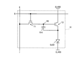
- FIG. 51 is a circuit diagram showing a configuration of a conventional general pixel circuit 91.
- the pixel circuit 91 is provided corresponding to each intersection of the plurality of data lines S and the plurality of scanning lines G arranged in the display unit.
- the pixel circuit 91 includes two transistors T1 and T2, one capacitor Cst, and one organic EL element OLED.
- the transistor T1 is an input transistor
- the transistor T2 is a drive transistor.
- the transistor T1 is provided between the data line S and the gate terminal of the transistor T2.
- a gate terminal is connected to the scanning line G, and a source terminal is connected to the data line S.
- the transistor T2 is provided in series with the organic EL element OLED.
- a drain terminal is connected to a power supply line that supplies a high-level power supply voltage ELVDD, and a source terminal is connected to an anode terminal of the organic EL element OLED.
- a power supply line that supplies the high-level power supply voltage ELVDD is hereinafter referred to as a “high-level power supply line”, and the high-level power supply line is given the same sign ELVDD as the high-level power supply voltage.
- the capacitor Cst one end is connected to the gate terminal of the transistor T2, and the other end is connected to the source terminal of the transistor T2.
- the cathode terminal of the organic EL element OLED is connected to a power supply line that supplies a low level power supply voltage ELVSS.
- the power supply line that supplies the low-level power supply voltage ELVSS is hereinafter referred to as “low-level power supply line”, and the same sign ELVSS as the low-level power supply voltage is attached to the low-level power supply line.
- a connection point between the gate terminal of the transistor T2, one end of the capacitor Cst, and the drain terminal of the transistor T1 is referred to as a “gate node VG” for convenience.
- the higher of the drain and the source is called the drain, but in the description of this specification, one is defined as the drain and the other is defined as the source. Therefore, the source potential is higher than the drain potential. May be higher.
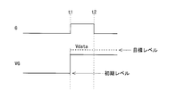
- FIG. 52 is a timing chart for explaining the operation of the pixel circuit 91 shown in FIG.
- the scanning line G Prior to time t1, the scanning line G is in a non-selected state. Therefore, before the time t1, the transistor T1 is in an off state, and the potential of the gate node VG maintains an initial level (for example, a level corresponding to writing in the previous frame).
- the scanning line G is selected and the transistor T1 is turned on.
- the data voltage Vdata corresponding to the luminance of the pixel (subpixel) formed by the pixel circuit 91 is supplied to the gate node VG via the data line S and the transistor T1.
- the potential of the gate node VG changes according to the data voltage Vdata.
- the capacitor Cst is charged to the gate-source voltage Vgs which is the difference between the potential of the gate node VG and the source potential of the transistor T2.
- the scanning line G is in a non-selected state.
- the transistor T1 is turned off, and the gate-source voltage Vgs held by the capacitor Cst is determined.
- the transistor T2 supplies a drive current to the organic EL element OLED according to the gate-source voltage Vgs held by the capacitor Cst. As a result, the organic EL element OLED emits light with a luminance corresponding to the drive current.
- a thin film transistor (TFT) is typically employed as a drive transistor.
- the characteristics of thin film transistors are likely to vary. Specifically, the threshold voltage tends to vary.
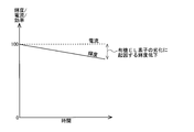
- the current efficiency decreases with time. Therefore, even if a constant current is supplied to the organic EL element, the luminance gradually decreases with time. As a result, image sticking occurs.
- an internal compensation technique in which the threshold voltage of the driving transistor is held in a capacitor provided between the gate and the source of the driving transistor in the pixel circuit, for example, under a predetermined condition.
- an external compensation technique for performing compensation processing by measuring the magnitude of the current flowing through the driving transistor with a circuit provided outside the pixel circuit and correcting the video signal based on the measurement result.
- Japanese Japanese translation of PCT publication No. 2008-523448 discloses an external compensation technique for correcting data based on the characteristics of a driving transistor and the characteristics of an organic EL element.
- Japanese Unexamined Patent Application Publication No. 2007-233326 discloses an external compensation technique that enables image display with uniform brightness regardless of the threshold voltage and electron mobility of a driving transistor.
- the compensation process is performed by detecting a slight current of about several tens of nanoamperes. For this reason, for example, when noise is mixed in the detection current due to the approach of the charged substance, an error that cannot be ignored is generated between the original current value and the measured value.
- an organic EL display device equipped with a touch panel has been commercially available. In this regard, the touch panel is relatively susceptible to noise. Therefore, it is conceivable that an error occurs between the original current value and the measured value due to the influence of noise emitted from the touch panel.
- an object of the present invention is to prevent a reduction in compensation accuracy due to noise in a display device that employs an external compensation technique to compensate for deterioration of circuit elements.
- n ⁇ m electro-optical elements whose luminance is controlled by current and driving transistors for controlling the current to be supplied to the electro-optical elements (n and m are 2).
- processing of the correction data update step based on the detection result in the characteristic detection step performed immediately before the noise is detected and the noise It is characterized in that at least one of the processes of the correction data update step based on the detection result in the characteristic detection step performed immediately after the point in time is detected is not performed.
- the characteristic detection step at least one characteristic of the driving transistor and the electro-optical element is detected for only one row of the pixel matrix
- the target frame period is defined as the frame period in which the processing of the characteristic detection step for the Z-th row (Z is an integer of 1 to n)
- the process of the correction data update step based on the detection result in the characteristic detection step performed in the target frame period is Without being performed, the process of the characteristic detection step for the Z-th row is also performed in the frame period next to the target frame period,
- noise equal to or higher than the reference value is not detected in the noise measurement step in the target frame period, and noise equal to or higher than the reference value is detected in the noise measurement step in a frame period subsequent to the target frame period.
- the correction data update step is not performed, and the characteristic detection step for the Z-th row is performed in a frame period two frames after the target frame period.
- the characteristic detection step at least one characteristic of the driving transistor and the electro-optical element is detected for only one row of the pixel matrix
- the process of the correction data update step based on the detection result in the characteristic detection step for the Z-th row is performed immediately before the characteristic detection step for the Z-th row. This is performed only when noise of the reference value or more is not detected in both the noise measurement step and the noise measurement step performed immediately after the characteristic detection step for the Z-th row.
- the noise measurement step is performed before and after the characteristic detection step.
- the noise measurement step is performed for each of a plurality of frame periods.
- the characteristic detection step includes A first characteristic detecting step for detecting a characteristic of the driving transistor; A second characteristic detecting step for detecting a characteristic of the electro-optic element,
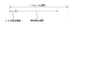
- One frame period includes a noise measurement period in which the process of the noise measurement step is performed, a selection period in which preparations for causing the electro-optical element to emit light are performed, and a light-emitting period in which light emission of the electro-optical element is performed,
- the processing of the first characteristic detection step is performed during the selection period
- the process of the second characteristic detection step is performed during the light emission period.
- the characteristic of the electro-optical element is detected by measuring the voltage of the anode of the electro-optical element in a state where a constant current is applied to the electro-optical element.
- the characteristic of the electro-optical element is detected by measuring a current flowing through the electro-optical element in a state where a constant voltage is applied to the electro-optical element. To do.
- the current flowing between the drain and the source of the driving transistor is measured in a state in which the voltage between the gate and the source of the driving transistor is set to a predetermined magnitude, so that the characteristic of the driving transistor is measured. Is detected.
- the display device further includes a touch panel,
- the characteristic detection step is not performed throughout a period in which a clock operation by the touch panel is performed.
- a twelfth aspect of the present invention is the eleventh aspect of the present invention,
- the touch panel performs a clock operation during a vertical blanking period,
- the characteristic detecting step is not performed throughout the vertical blanking period.
- n ⁇ m electro-optic elements whose luminance is controlled by current and driving transistors for controlling the current to be supplied to the electro-optic elements (n and m are 2).
- a display device having a pixel matrix of n rows ⁇ m columns composed of pixel circuits of the above integer), A pixel circuit driver that drives the n ⁇ m pixel circuits while performing a characteristic detection process for detecting at least one characteristic of the drive transistor and the electro-optic element;
- a correction data storage unit for storing correction data for correcting the video signal;
- a correction data update process for updating correction data stored in the correction data storage unit based on a detection result in the characteristic detection process, and a video signal to be supplied to the n ⁇ m pixel circuits is the correction data.
- a noise measurement unit for measuring noise The control unit controls the operation of the pixel circuit drive unit so that the characteristic detection process is not performed immediately after the noise is detected when noise equal to or higher than a reference value is detected by the noise measurement unit.
- the correction data update process based on the detection result of the characteristic detection process performed at a time near the time when the noise is detected is not performed.
- a fourteenth aspect of the present invention is the thirteenth aspect of the present invention.
- the control unit updates the correction data based on the detection result of the characteristic detection process performed immediately before the noise is detected.
- at least one of the correction data update processing based on the detection result of the characteristic detection processing performed immediately after the noise is detected is not performed.
- a monitor line provided so as to correspond to each column of the pixel matrix;
- the pixel circuit driving unit includes a characteristic detection unit that performs the characteristic detection process by measuring a current flowing through the monitor line or a voltage at a predetermined position on the monitor line.
- a sixteenth aspect of the present invention is the fifteenth aspect of the present invention,
- the noise measurement unit shares the same circuit as the characteristic detection unit, When noise is measured by the noise measuring unit, the monitor line is electrically disconnected from the electro-optic element and the driving transistor.
- the noise measurement unit is provided outside the organic EL panel including the pixel matrix, separately from the characteristic detection unit.
- K is an integer of 2 to m
- One of the K monitor lines is electrically connected to the characteristic detector, The monitor line that is not electrically connected to the characteristic detection unit is in a high impedance state.
- a touch panel controls the operation of the pixel circuit driving unit so that the characteristic detection process is stopped during a period in which a clock operation by the touch panel is performed.
- the touch panel performs a clock operation during a vertical blanking period
- the control unit controls the operation of the pixel circuit driving unit so that the characteristic detection process stops during a vertical blanking period.
- a pixel circuit including an electro-optical element (for example, an organic EL element) whose luminance is controlled by a current and a driving transistor for controlling a current to be supplied to the electro-optical element.
- a noise measuring step for measuring noise is included in the driving method of the display device. If the magnitude of the noise detected in the noise measurement step is less than the reference value, the video signal is corrected using correction data obtained in consideration of the detection results of the characteristics of the drive transistor and the electro-optical element. Since the video signal corrected in this way is supplied to the pixel circuit, a driving current having such a magnitude as to compensate for deterioration of the driving transistor and the electro-optical element is supplied to the electro-optical element.
- the correction data is not updated.
- the correction data is not updated when there is a non-negligible error between the original current value and the measured value regarding the detection current for external compensation for the deterioration of the circuit element. Therefore, a reduction in compensation accuracy due to an inappropriate value of correction data is prevented.
- an external compensation technique is employed to compensate for circuit element degradation, it is possible to prevent a reduction in compensation accuracy due to noise.
- the rows subjected to characteristic detection are maintained during the period when noise is generated. For this reason, it is possible to prevent the number of characteristic detections from being different for each row. As a result, it is possible to uniformly compensate for deterioration of the drive transistor and the electro-optical element over the entire screen, and effectively prevent variations in luminance.
- the correction data is obtained only when the noise magnitude is less than the reference value in both the noise measurement step immediately before the characteristic detection step and the noise measurement step immediately after the characteristic detection step. Is updated.
- the correction data is updated in consideration of the noise state in the period before and after the period in which the characteristic detection is performed, so that the compensation accuracy is further reduced due to an inappropriate value of the correction data. Effectively prevented.
- the same effect as in the first aspect of the present invention can be obtained while reducing the frequency of noise measurement.
- the characteristic of the driving transistor is detected during the selection period, and the characteristic of the electro-optical element is detected during the light emission period of the electro-optical element.
- a constant current is supplied to the electro-optical element that detects the characteristic. Therefore, by adjusting the time for supplying a constant current to the electro-optical element, it becomes possible to cause the electro-optical element to emit light with a desired luminance.
- the measurement time for detecting the characteristics of the electro-optic element can be shortened.
- the characteristics of the drive transistor can be detected relatively easily.
- the eleventh aspect of the present invention in a display device that employs an external compensation technique to compensate for circuit element degradation, even if a touch panel is mounted, a reduction in compensation accuracy due to noise is prevented. It becomes possible to do.
- the same effect as in the first aspect of the present invention can be achieved in the invention of the display device.
- the same effect as in the second aspect of the present invention can be achieved in the invention of the display device.
- a drive transistor or an electro-optical element is measured by measuring a current flowing through a monitor line provided to correspond to each column of the pixel matrix or a voltage at a predetermined position on the monitor line.
- the display device configured to detect this characteristic, it is possible to prevent a reduction in compensation accuracy due to noise.
- the sixteenth aspect of the present invention it is not necessary to provide a noise measurement circuit separately from the characteristic detection unit. For this reason, it is possible to prevent a decrease in compensation accuracy due to noise while suppressing an increase in circuit area.
- noise can be measured at an arbitrary timing during the frame period.
- one characteristic detection unit is shared by a plurality of monitor lines. For this reason, it is possible to prevent a decrease in compensation accuracy due to noise while suppressing an increase in circuit area.
- the same effect as in the eleventh aspect of the present invention can be achieved in the invention of the display device.
- the same effect as that of the twelfth aspect of the present invention can be achieved in the invention of the display device.
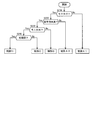
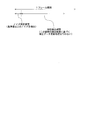
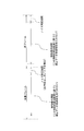
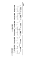
- FIG. 5 is a flowchart for explaining an outline of a driving method when paying attention to a monitor column in a monitor row in the first embodiment of the present invention. It is a block diagram which shows the whole structure of the active matrix type organic electroluminescent display apparatus which concerns on the said 1st Embodiment. 5 is a timing chart for explaining an operation of a gate driver in the first embodiment. 5 is a timing chart for explaining an operation of a gate driver in the first embodiment. 5 is a timing chart for explaining an operation of a gate driver in the first embodiment.
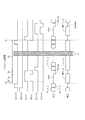
- FIG. 3 is a block diagram illustrating a schematic configuration of a signal conversion circuit in the first embodiment. It is a figure which shows the structure of the pixel circuit and monitor circuit in the said 1st Embodiment.
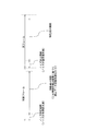
- FIG. 6 is a diagram for describing conditions under which correction data update processing based on a result of characteristic detection in a certain frame is performed in the first embodiment.
- the said 1st Embodiment it is a figure for demonstrating the flow of an electric current when normal operation is performed.
- the first embodiment it is a timing chart for explaining the operation of a pixel circuit (referred to as a pixel circuit of i rows and j columns) included in a monitor column of monitor rows (detected during a noise measurement period). If the noise level is below the reference value).
- it is a timing chart for explaining the operation of a pixel circuit (referred to as a pixel circuit of i rows and j columns) included in a monitor column of monitor rows (detected during a noise measurement period). When the noise level is above the reference value).
- the said 1st Embodiment it is a figure for demonstrating the flow of the electric current in a noise measurement period. In the said 1st Embodiment, it is a figure for demonstrating the flow of the electric current in a TFT characteristic detection period. In the said 1st Embodiment, it is a figure for demonstrating the application to the data line of the reference voltage in a TFT characteristic detection period. In the said 1st Embodiment, it is a figure for demonstrating the flow of the electric current in the light emission period. In the said 1st Embodiment, it is a figure for demonstrating adjustment of the light emission time of an organic EL element.
- the said 1st Embodiment it is a figure for demonstrating the difference in the length of the light emission period in a monitoring line and a non-monitoring line. It is a flowchart for demonstrating the control algorithm in the said 1st Embodiment. It is a figure for demonstrating each control in the said 1st Embodiment. 6 is a flowchart for explaining a procedure for updating an offset memory and a gain memory in the first embodiment. It is a figure which shows the structure of the video signal correction
- FIG. 10 is a flowchart for explaining an outline of a driving method when attention is paid to a monitor column in a monitor row in the first modification of the first embodiment. It is a figure for demonstrating operation
- the 5th modification of the said 1st Embodiment it is a figure for demonstrating the relationship between a noise measurement period and a characteristic detection period. It is a figure for demonstrating operation
- FIG. 24 is a timing chart for explaining an operation of a pixel circuit (referred to as a pixel circuit of i rows and j columns) included in a monitor column of monitor rows in an eighth modification of the first embodiment. It is a block diagram which shows the whole structure of the active matrix type organic electroluminescent display apparatus which concerns on the 2nd Embodiment of this invention.
- FIG. 12 is a timing chart for explaining the operation of a pixel circuit (referred to as a pixel circuit of i rows and j columns) included in a monitor column of the monitor rows in the second embodiment.
- a pixel circuit referred to as a pixel circuit of i rows and j columns
- It is a flowchart for demonstrating the control algorithm in the said 3rd Embodiment. It is a figure for demonstrating each control in the said 3rd Embodiment. It is a figure for demonstrating the effect in the said 3rd Embodiment.
- It is a circuit diagram which shows the structure of the conventional general pixel circuit. 52 is a timing chart for explaining the operation of the pixel circuit shown in FIG. 51.
- TFT characteristic the characteristic of the driving transistor provided in the pixel circuit
- OLED characteristic the characteristic of the organic EL element provided in the pixel circuit
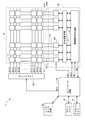
- FIG. 2 is a block diagram showing the overall configuration of the active matrix organic EL display device 1 according to the first embodiment of the present invention.
- the organic EL display device 1 includes a display unit (organic EL panel) 10, a control circuit 20, a source driver (data line driving circuit) 30, a gate driver (scanning line driving circuit) 40, an offset memory 51, and a gain memory 52.
- a display unit organic EL panel
- the source driver data line driving circuit
- a gate driver scanning line driving circuit
- the offset memory 51 and the gain memory 52 may be physically constituted by one memory.
- a control unit is realized by the control circuit 20
- a pixel circuit driving unit is realized by the source driver 30 and the gate driver 40
- a correction data storage unit is realized by the offset memory 51 and the gain memory 52.
- the display unit 10 is provided with m data lines S (1) to S (m) and n scanning lines G1 (1) to G1 (n) orthogonal thereto.
- the extending direction of the data lines is defined as the Y direction
- the extending direction of the scanning lines is defined as the X direction.
- Components along the Y direction may be referred to as “columns”
- components along the X direction may be referred to as “rows”.
- the display unit 10 is provided with m monitor lines M (1) to M (m) so as to correspond to the m data lines S (1) to S (m) on a one-to-one basis. ing.
- the data lines S (1) to S (m) and the monitor lines M (1) to M (m) are parallel to each other.
- the display unit 10 is provided with n monitor control lines G2 (1) to G2 (n) so as to correspond to the n scanning lines G1 (1) to G1 (n) on a one-to-one basis.
- the scanning lines G1 (1) to G1 (n) and the monitor control lines G2 (1) to G2 (n) are parallel to each other.
- the display unit 10 has n ⁇ m so as to correspond to the intersections of the n scanning lines G1 (1) to G1 (n) and the m data lines S (1) to S (m).
- Pixel circuits 11 are provided. By providing n ⁇ m pixel circuits 11 in this manner, a pixel matrix of n rows ⁇ m columns is formed in the display unit 10.
- the display unit 10 is provided with a high level power supply line for supplying a high level power supply voltage and a low level power supply line for supplying a low level power supply voltage.
- the data lines are simply represented by a symbol S.
- the monitor lines are simply represented by the symbol M, and the n scan lines G1 (1) to G1 (n) If it is not necessary to distinguish the monitor lines from each other, the scanning line is simply indicated by G1, and if it is not necessary to distinguish the n monitor control lines G2 (1) to G2 (n) from each other, the monitor control lines are simply denoted by reference numerals. Represented by G2.
- the control circuit 20 controls the operation of the source driver 30 by supplying the data signal DA, the source control signal SCTL, and the switching control signal SW to the source driver 30, and transmits the gate control signal GCTL to the gate driver 40.
- the operation of the driver 40 is controlled.
- the source control signal SCTL includes, for example, a source start pulse, a source clock, and a latch strobe signal.
- the gate control signal GCTL includes, for example, a gate start pulse and a gate clock.
- the control circuit 20 receives the monitor data MO given from the source driver 30 and updates the offset memory 51 and the gain memory 52.
- the monitor data MO is data (including noise data to be described later) measured for obtaining TFT characteristics and OLED characteristics.
- the gate driver 40 is connected to n scanning lines G1 (1) to G1 (n) and n monitor control lines G2 (1) to G2 (n).
- the gate driver 40 includes a shift register and a logic circuit.
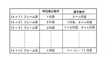
- TFT characteristics and OLED characteristics for the third row is performed. In this way, detection of TFT characteristics and OLED characteristics for n rows is performed over an n frame period. However, TFT characteristics and OLED characteristics are not detected in a column in which noise of a reference value or more is detected in each frame.
- n scanning lines G1 (1) to G1 (n) and n monitor control lines G2 (1) to G2 (n) are driven as shown in FIG. 3 at the (k + 1) th frame, driven at the (k + 2) th frame as shown in FIG. 4, and at the (k + n) th frame.
- the high level state is an active state.
- a period in which the scanning line G1 is in an active state is referred to as a “selection period”. This selection period is a period for preparing to emit light from the organic EL element provided in the pixel circuit 11. As can be understood from FIGS.
- the monitor control line G2 corresponding to the monitor row is in an active state for a predetermined period from the beginning of the selection period and in an inactive state for the remaining period of the selection period. In the period up to about one frame period after the start of the selection period, it becomes active again.
- the gate driver 40 is driven so that the n scanning lines G1 (1) to G1 (n) and the n monitor control lines G2 (1) to G2 (n) are driven as described above. It is configured.
- the source driver 30 is connected to m data lines S (1) to S (m) and m monitor lines M (1) to M (m).
- the source driver 30 includes a drive signal generation circuit 31, a signal conversion circuit 32, and an output unit 33 including m output circuits 330.
- the m output circuits 330 in the output unit 33 respectively correspond to the corresponding data line S and m monitor lines M (1) to M (m) among the m data lines S (1) to S (m). Are connected to the corresponding monitor line M.
- the drive signal generation circuit 31 includes a shift register, a sampling circuit, and a latch circuit.
- the shift register sequentially transfers the source start pulse from the input end to the output end in synchronization with the source clock.
- a sampling pulse corresponding to each data line S is output from the shift register.
- the sampling circuit sequentially stores the data signals DA for one row according to the timing of the sampling pulse.
- the latch circuit fetches and holds the data signal DA for one row stored in the sampling circuit according to the latch strobe signal.
- FIG. 6 is a block diagram showing a schematic configuration of the signal conversion circuit 32.
- the signal conversion circuit 32 includes a gradation signal generation circuit 321 and a monitor circuit 322.
- the gradation signal generation circuit 321 includes a D / A converter.
- the data signal DA for one row held in the latch circuit in the drive signal generation circuit 31 as described above is converted into an analog voltage by the D / A converter in the gradation signal generation circuit 321.
- the converted analog voltage is applied to the output circuit 330 in the output unit 33.
- the monitor circuit 322 includes an A / D converter.
- the analog voltage that appears on the monitor line M and that represents the TFT characteristics and the OLED characteristics, and the analog voltage that represents the magnitude of the noise that appears on the monitor line M are included in the monitor data MO that is a digital signal. Converted.
- the monitor data MO is given to the control circuit 20 via the drive signal generation circuit 31. A detailed description of the monitor circuit 322 will be given later.
- the output circuit 330 in the output unit 33 applies the analog voltage supplied from the gradation signal generation circuit 321 in the signal conversion circuit 32 to the data line S as a data voltage through the buffer.
- the output circuit 330 in the output unit 33 switches the connection destination of the monitor line M based on the switching control signal SW. A detailed description thereof will be described later.
- the offset memory 51 and the gain memory 52 store correction data used for correcting a video signal sent from the outside.
- the offset memory 51 stores an offset value as correction data
- the gain memory 52 stores a gain value as correction data.
- the number of offset values and gain values equal to the number of pixels in the display unit 10 are stored in the offset memory 51 and the gain memory 52, respectively.
- a buffer memory for temporarily holding an offset value hereinafter referred to as “offset value buffer”
- gain value buffer a buffer memory for temporarily holding a gain value
- the control circuit 20 updates the offset value in the offset memory 51 and the gain value in the gain memory 52 based on the monitor data MO given from the source driver 30.
- control circuit 20 reads the offset value stored in the offset memory 51 and the gain value stored in the gain memory 52 and corrects the video signal. Data obtained by the correction is sent to the source driver 30 as a data signal DA. Further, the control circuit 20 controls the operations of the gate driver 40 and the source driver 30 relating to the detection of TFT characteristics and OLED characteristics based on the monitor data MO as noise data.
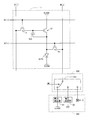
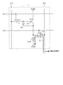
- FIG. 7 is a diagram illustrating the configuration of the pixel circuit 11 and the monitor circuit 322.
- the pixel circuit 11 illustrated in FIG. 7 is the pixel circuit 11 of i rows and j columns.
- the pixel circuit 11 includes one organic EL element OLED, three transistors T1 to T3, and one capacitor Cst.
- the transistor T1 functions as an input transistor for selecting a pixel
- the transistor T2 functions as a drive transistor for controlling supply of current to the organic EL element OLED
- the transistor T3 controls whether to detect TFT characteristics or OLED characteristics. Functions as a monitor control transistor.
- the transistor T1 is provided between the data line S (j) and the gate terminal of the transistor T2.
- a gate terminal is connected to the scanning line G1 (i), and a source terminal is connected to the data line S (j).
- the transistor T2 is provided in series with the organic EL element OLED.
- the gate terminal is connected to the drain terminal of the transistor T1, the drain terminal is connected to the high-level power supply line ELVDD, and the source terminal is connected to the anode terminal of the organic EL element OLED.
- the gate terminal is connected to the monitor control line G2 (i)
- the drain terminal is connected to the anode terminal of the organic EL element OLED
- the source terminal is connected to the monitor line M (j).
- the capacitor Cst one end is connected to the gate terminal of the transistor T2, and the other end is connected to the source terminal of the transistor T2.
- the cathode terminal of the organic EL element OLED is connected to the low level power line ELVSS.
- the transistors T1 to T3 in the pixel circuit 11 are all n-channel type.
- oxide TFTs thin film transistors using an oxide semiconductor as a channel layer are employed for the transistors T1 to T3.
- the oxide semiconductor layer is, for example, an In—Ga—Zn—O-based semiconductor layer.
- the oxide semiconductor layer includes, for example, an In—Ga—Zn—O-based semiconductor.
- An In—Ga—Zn—O-based semiconductor is a ternary oxide of In (indium), Ga (gallium), and Zn (zinc).
- a TFT having an In—Ga—Zn—O-based semiconductor layer has high mobility (mobility more than 20 times that of an amorphous silicon TFT) and low leakage current (leakage less than 1/100 that of an amorphous silicon TFT). Therefore, it is suitably used as a driving TFT (the transistor T2) and a switching TFT (the transistor T1) in the pixel circuit.
- a driving TFT the transistor T2
- a switching TFT the transistor T1 in the pixel circuit.
- the In—Ga—Zn—O-based semiconductor may be amorphous, may include a crystalline portion, and may have crystallinity.
- a crystalline In—Ga—Zn—O-based semiconductor in which the c-axis is oriented substantially perpendicular to the layer surface is preferable.
- Such a crystal structure of an In—Ga—Zn—O-based semiconductor is disclosed, for example, in Japanese Unexamined Patent Publication No. 2012-134475.
- the oxide semiconductor layer may include another oxide semiconductor instead of the In—Ga—Zn—O-based semiconductor.
- Zn—O based semiconductor ZnO
- In—Zn—O based semiconductor IZO (registered trademark)
- Zn—Ti—O based semiconductor ZTO
- Cd—Ge—O based semiconductor Cd—Pb—O based
- CdO cadmium oxide
- Mg—Zn—O based semiconductors In—Sn—Zn—O based semiconductors (eg, In 2 O 3 —SnO 2 —ZnO), In—Ga—Sn—O based semiconductors, etc. You may go out.
- the monitor circuit 322 includes a current measurement unit 37 and a voltage measurement unit 38.
- the monitor circuit 322 implements a characteristic detection unit and a noise measurement unit.
- the noise measurement unit shares the same circuit as the characteristic detection unit.
- the relationship between the current measuring unit 37 and the voltage measuring unit 38 and the monitor line M (j) is controlled based on a switching control signal SW given from the control circuit 20 to the output circuit 330.
- a switch hereinafter referred to as “monitor line switch” 331 provided in the output circuit 330 is in a state where the monitor line M (j) is connected to the current measuring unit 37.
- a state connected to the voltage measuring unit 38 or a high impedance state is assumed. In FIG. 7, only a part of the configuration of the output circuit 330 is shown.
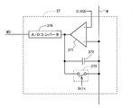
- FIG. 8 is a diagram illustrating a configuration example of the current measuring unit 37.
- the current measurement unit 37 includes an operational amplifier 371, a capacitor 372, a switch 373, and an A / D converter 374.
- the operational amplifier 371 the non-inverting input terminal is connected to the low-level power supply line ELVSS, and the inverting input terminal is connected to the monitor line M.
- the capacitor 372 and the switch 373 are provided between the output terminal of the operational amplifier 371 and the monitor line M.
- the current measuring unit 37 is configured by an integrating circuit. In such a configuration, when the switch 373 is turned on by the control clock signal Sclk, the output terminal and the inverting input terminal of the operational amplifier 371 are short-circuited.
- the potential of the output terminal of the operational amplifier 371 and the potential of the monitor line M become equal to the potential of the low level power supply line ELVSS.
- the switch 373 is switched from the on state to the off state by the control clock signal Sclk.
- the potential of the output terminal of the operational amplifier 371 changes according to the magnitude of the current flowing through the monitor line M.
- the change in potential is reflected in the digital signal output from the A / D converter 374.
- the digital signal is output from the current measuring unit 37 as monitor data MO.
- a current for obtaining TFT characteristics and a noise current generated in the monitor line M during a noise measurement period described later are measured by the current measuring unit 37. Data indicating the magnitude of the noise current measured by the current measuring unit 37 is sent to the control circuit 20 as noise data.
- FIG. 9 is a diagram illustrating a configuration example of the voltage measurement unit 38.
- the voltage measuring unit 38 includes an amplifier 381 and an A / D converter 382.
- the voltage between the node 383 and the low-level power line ELVSS is amplified by the amplifier 381 in a state where a constant current is passed through the monitor line M by the constant current source 36.
- the amplified voltage is converted into a digital signal by the A / D converter 382.
- the digital signal is output from the voltage measurement unit 38 as monitor data MO.
- the voltage measurement unit 38 measures a voltage for obtaining the OLED characteristic.
- a driving method in the present embodiment will be described.
- a row in which a selection period longer than usual when an arbitrary frame is focused is referred to as a “monitor row”.
- the Q column (Q is an integer of 1 or more and m or less) in the monitor row is the detection target column of the TFT characteristics and the OLED characteristics.
- a column to be detected for TFT characteristics and OLED characteristics is referred to as a “monitor column”
- a column other than the monitor column is referred to as a “non-monitor column”.
- the detection operation is performed for the monitor row, and a normal operation is performed for the non-monitor row. That is, if the frame in which the TFT characteristic and the OLED characteristic for the first row are detected is defined as the (k + 1) th frame, the operation of each row changes as shown in FIG. However, as described above, the characteristic detection operation is not performed in the column in which noise equal to or higher than the reference value is detected.
- the offset memory 51 and the gain memory 52 are updated using the detection result. Then, the video signal is corrected using the correction data stored in the offset memory 51 and the gain memory 52.
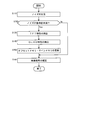
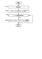
- FIG. 1 is a flowchart for explaining an outline of a driving method when paying attention to a monitor column in a monitor row in the present embodiment.
- noise generated on the monitor line M is measured (step S110).
- step S110 noise generated on the monitor line M is measured.
- step S120 it is determined whether or not the magnitude of noise measured in step S110 is less than a reference value (step S120). As a result, if the noise magnitude is less than the reference value, the process proceeds to step S130, and if the noise magnitude is greater than or equal to the reference value, the process proceeds to step S160.
- step S160 is performed after the processing of step S130, step S140, and step S150, and if the magnitude of noise is greater than or equal to the reference value.
- the process of step S160 is performed without performing the processes of step S130, step S140, and step S150.
- step S130 the TFT characteristics are detected.
- step S140 the OLED characteristic is detected.
- step S150 the offset memory 51 and the gain memory 52 are updated using the detection result in step S130 and the detection result in step S140.
- step S160 the correction of the video signal sent from the outside is performed using the correction data stored in the offset memory 51 and the gain memory 52.
- a noise measurement step is realized by step S110
- a characteristic detection step is realized by steps S130 and S140
- a correction data update step is realized by step S150
- a video signal correction step is realized by step S160.
- the first characteristic detection step is realized by step S130
- the second characteristic detection step is realized by step S140.
- the pixel circuit driving unit (the source driver 30 and the gate driver 40) performs a process of detecting at least one characteristic of the transistor T2 and the organic EL element OLED while performing n ⁇ The m pixel circuits 11 are driven.
- the control unit updates the correction data stored in the offset memory 51 and the gain memory 52 based on the result of the characteristic detection and supplies the correction data to the n ⁇ m pixel circuits 11. While performing the process of correcting the video signal based on the correction data stored in the offset memory 51 and the gain memory 52, the operation of the pixel circuit driving unit (source driver 30 and gate driver 40) is controlled.
- FIG. 12 is a diagram for explaining conditions under which correction data update processing is performed based on the result of characteristic detection in a certain frame (herein referred to as “target frame”).
- target frame a certain frame
- the magnitude of noise detected during the noise measurement period of the target frame is less than the reference value
- correction data update processing based on the result of characteristic detection in the target frame is performed. Is called. That is, in the present embodiment, the result of noise measurement in frames before and after the target frame does not affect the correction data update process based on the result of characteristic detection in the target frame.
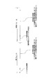
- FIG. 13 is a diagram for explaining the operation when noise of a reference value or more is detected in the present embodiment.
- the monitor sequence when noise equal to or higher than the reference value is detected during the noise measurement period of the target frame, characteristic detection is not performed in the target frame (see also FIG. 1). .
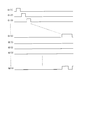
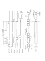
- FIG. 15 and 16 are timing charts for explaining the operation of the pixel circuit 11 (referred to as the pixel circuit 11 in i row and j column) included in the monitor column of the monitor rows.
- “one frame period” is represented with reference to the start time of the noise measurement period Tn in the frame in which the i-th row is the monitor row.
- FIG. 15 is a timing chart when the magnitude of noise detected during the noise measurement period Tn is less than the reference value.
- FIG. 16 shows the magnitude of noise detected during the noise measurement period Tn. It is a timing chart in the case of being above.
- a noise measurement period Tn and a period for detecting TFT characteristics (hereinafter referred to as “TFT characteristic detection period”) Ta and A period (hereinafter referred to as “black writing period”) Tb for writing data corresponding to black display and a period (hereinafter referred to as “light emitting period”) Tc for causing the organic EL element OLED to emit light.
- TFT characteristic detection period a period for detecting TFT characteristics
- black writing period A period for writing data corresponding to black display
- the first predetermined period in the selection period is the TFT characteristic detection period Ta
- the period other than the TFT characteristic detection period Ta in the selection period is the black writing period Tb.
- the monitor line M (j) of the monitor column is connected to the current measurement unit 37 by the switching control signal SW.
- the switch 373 is switched from the on state to the off state.
- the scanning line G1 (i) and the monitor control line G2 (i) are in an active state (see FIGS. 15 and 16). Accordingly, the transistor T1 and the transistor T3 are turned on. If the noise detected in the noise measurement period Tn is less than the reference value, the reference voltage Vref for detecting the TFT characteristics is applied to the data line S (j) in the TFT characteristic detection period Ta (FIG. 15). As a result, the reference voltage Vref is written, and the transistor T2 is also turned on. As a result, as indicated by an arrow 72 in FIG. 18, the current flowing through the transistor T2 is output to the monitor line M (j) through the transistor T3.
- the monitor line M (j) is connected to the current measuring unit 37 by the switching control signal SW during the TFT characteristic detection period Ta.
- the current (sink current) output to the monitor line M (j) is measured by the current measuring unit 37.
- the magnitude of the current flowing between the drain and source of the transistor T2 is measured in a state where the voltage between the gate and source of the transistor T2 is set to a predetermined level (the magnitude of the reference voltage Vref). TFT characteristics are detected.
- first reference voltage Vref1 and second reference voltage Vref2 are applied to the data line S (j) as the reference voltage Vref in the TFT characteristic detection period Ta. ).
- first reference voltage Vref1 and second reference voltage Vref2 are applied to the data line S (j) as the reference voltage Vref in the TFT characteristic detection period Ta.
- the data voltage D (i, j) corresponding to the target luminance is applied to the data line S (j) in the TFT characteristic detection period Ta. (See FIG. 16). As a result, the data voltage D (i, j) is written, and the transistor T2 is turned on. Note that after writing based on the data voltage D (i, j) is performed in the selection period (a period including the TFT characteristic detection period Ta and the black writing period Tb), the scanning line G1 (i) is in an inactive state. Thus, the transistor T1 is maintained in the off state.
- the driving current corresponding to the data voltage D (i, j) is supplied to the organic EL element OLED as in the normal operation,
- the organic EL element OLED emits light with a luminance corresponding to the drive current.
- the scanning line G1 (i) is maintained in an active state, and the monitor control line G2 (i) is in an inactive state (see FIG. 15). Accordingly, the transistor T1 is maintained in the on state, and the transistor T3 is in the off state. If the noise detected during the noise measurement period Tn is less than the reference value, the voltage Vblack corresponding to black display is applied to the data line S (j) during the black writing period Tb (see FIG. 15). Therefore, the transistor T2 is turned off. Thus, no current flows through the transistor T2.
- “the difference between the offset value stored in the offset memory 51 and the offset value obtained in the TFT characteristic detection period Ta” and “the gain memory 52 are stored.
- a voltage sum of “a voltage corresponding to the light emission voltage” calculated from the gain value and the gain value obtained in the TFT characteristic detection period Ta is applied to the monitor line M (j).
- a voltage corresponding to the degree of deterioration of the organic EL element OLED is applied to the monitor line M (j) before the light emission period Tc, and the length of the charging time in the light emission period Tc is shortened.
- the scanning line G1 (i) is in an inactive state, and the monitor control line G2 (i) is in an active state (see FIG. 15).
- the monitor line M (j) is connected to the voltage measurement unit 38 in the period for detecting the OLED characteristic in the light emission period Tc.
- the constant current I (i, j) is supplied to the monitor line M (j).
- a data current that is a constant current is supplied from the monitor line M (j) to the organic EL element OLED as indicated by an arrow 73 in FIG.
- the voltage measuring unit 38 measures the light emission voltage of the organic EL element OLED.
- the OLED characteristic is detected by measuring the voltage of the anode of the organic EL element OLED in a state where a constant current is applied to the organic EL element OLED.
- the data current supplied to the organic EL element OLED in the light emission period Tc is a constant current.
- the length of time during which the organic EL element OLED emits light is adjusted.
- the constant current is set to a current corresponding to white display, the light emission time is lengthened as the gradation is higher, and the light emission time is shortened as the gradation is lower.
- the period Tc1 in which the monitor line M is connected to the voltage measurement unit 38 is lengthened as the gray level is high, and the monitor line M is current as the gray level is low.
- a period (or a period during which the monitor line M is in a high impedance state) connected to the measurement unit 37 is lengthened.
- the lengths of the periods Tc1 and Tc2 are adjusted based on the deterioration correction coefficient obtained from the difference between the gain value stored in the gain memory 52 and the gain value obtained in the TFT characteristic detection period Ta. .
- the length of time that the organic EL element OLED emits light is adjusted so that the integrated value of the light emission current in one frame period becomes a value corresponding to a desired gradation. In other words, the length of time for applying a constant current to the organic EL element OLED is adjusted according to the target luminance.
- the current value is changed during the light emission period Tc, and characteristics (current-voltage) at a plurality of operating points are changed. (Characteristic) may be measured.
- the current value may be changed according to the gradation while the length of time during which the organic EL element OLED emits light is constant.
- the magnitude of the current supplied to the monitor line M is obtained based on the deterioration correction coefficient obtained from the difference between the gain value stored in the gain memory 52 and the gain value obtained in the TFT characteristic detection period Ta. And good. Since the gain memory 52 stores gain values considering both TFT characteristics and OLED characteristics, the gain value stored in the gain memory 52 and the gain value obtained in the TFT characteristic detection period Ta are The difference is a value representing the OLED characteristic.
- the length of the selection period is longer in the monitor row than in the non-monitor row. Therefore, the length of the light emission period is different between the monitor row and the non-monitor row. Therefore, the data current is adjusted so that the integrated value of the light emission current in one frame period becomes a value corresponding to a desired gradation.
- the detection of the OLED characteristic is not performed for the pixels that display black or nearly black (pixels that perform low gradation display) in the pixel matrix of n rows ⁇ m columns. To do. Thereby, unnecessary light emission can be prevented. Since the organic EL element OLED does not deteriorate if it does not emit light, it is not necessary to detect the characteristics.
- FIG. 23 is a flowchart for explaining the control algorithm.
- FIG. 24 is a diagram for explaining each control.
- the control circuit 20 controls the operations of the source driver 30 and the gate driver 40 based on this control algorithm.
- a procedure for determining a control method for data to be processed data indicating rows, columns, and gradations (hereinafter referred to as “target data”) will be described with reference to FIG.
- step S210 it is determined whether the target data is monitor row data. If the target data is not the monitor row data, the control method for the target data is “control A1”. If the target data is monitor row data, the determination in step S220 is further performed. In step S220, it is determined whether or not the magnitude of noise detected during the noise measurement period Tn is less than a reference value. If the magnitude of the noise is greater than or equal to the reference value, the control method for the target data is “control A2”. If the magnitude of the noise is less than the reference value, the determination in step S230 is further performed. In step S230, it is determined whether the target data is monitor row data. If the target data is not data in the monitor row, the control method for the target data is “control B”.
- step S240 it is determined whether or not the target data is low gradation data (gradation data for displaying black or gradation data for displaying substantially black). If the target data is not low gradation data, the control method for the target data is “control C”. If the target data is low gradation data, the control method for the target data is “control D”.
- control A1”, “control A2”, “control B”, “control C”, and “control D” will be described with reference to FIG.
- Control A1 is a control method for non-monitor row data. Since it is not necessary to detect the characteristics, the scanning line G1 (i) is in an active state (high level state) only for one normal horizontal scanning period, and the previous state is maintained for the monitor control line G2 (i). The In addition, since it is only necessary to perform normal display, a data voltage corresponding to normal gradation data is applied to the data line S (j). The previous state of the monitor line switch 331 after the noise measurement is maintained. Since the characteristic detection is not performed, the correction data is not updated.
- Control A2 is a control method for monitor row data in which noise equal to or higher than a reference value is detected in the noise measurement period Tn in the monitor row data. Since the target data is monitor row data, the scanning line G1 (i) is in an active state for the total period of one normal horizontal scanning period and the TFT characteristic detection period Ta. The previous state is maintained for the monitor control line G2 (i). In addition, since it is only necessary to perform normal display, a data voltage corresponding to normal gradation data is applied to the data line S (j). The previous state of the monitor line switch 331 after the noise measurement is maintained. Since the characteristic detection is not performed, the correction data is not updated.
- Control B is a control method for the data in the non-monitor column among the data in the monitor row. Since the target data is monitor row data, the scanning line G1 (i) is in an active state for the total period of one normal horizontal scanning period and the TFT characteristic detection period Ta. In addition, the monitor control line G2 (i) corresponding to the monitor row is activated during the TFT characteristic detection period Ta and the light emission period Tc. However, since the target data is non-monitor column data and it is not necessary to detect characteristics, the monitor line switch 331 after noise measurement is turned off (the monitor line M (j) becomes high impedance). ).
- a data voltage corresponding to data obtained by multiplying normal gradation data by a correction coefficient k (k is a value near 1) is applied to the data line S (j).
- the reason why the correction coefficient k is provided is that, since the transistor T3 is in the on state, the data voltage needs to be larger than the original depending on the wiring capacity of the monitor line M (j). Since the characteristic detection is not performed, the correction data is not updated.
- Control C is a control method for data other than the low gradation data among the data whose characteristics are to be detected. Since the target data is data whose characteristics are to be detected, the scanning line G1 (i) is in an active state for the total period of the normal one horizontal scanning period and the TFT characteristic detection period Ta. In addition, the monitor control line G2 (i) corresponding to the monitor row is activated during the TFT characteristic detection period Ta and the light emission period Tc. A voltage corresponding to black display is applied to the data line S (j) in the black writing period Tb in order to turn off the transistor T2.
- the monitor line switch 331 After the low level power supply voltage ELVSS is supplied to the monitor line M (j) to detect the TFT characteristics, a gradation signal is supplied to detect the OLED characteristics while causing the organic EL element OLED to emit light. Since the TFT characteristic and the OLED characteristic are detected, the correction data is updated.
- Control D is a control method for low gradation data in data whose characteristics are to be detected. Since the target data is data whose characteristics are to be detected, the scanning line G1 (i) is in an active state for the total period of the normal one horizontal scanning period and the TFT characteristic detection period Ta. In addition, the monitor control line G2 (i) corresponding to the monitor row is activated during the TFT characteristic detection period Ta and the light emission period Tc. A voltage corresponding to black display is applied to the data line S (j) in the black writing period Tb in order to turn off the transistor T2.
- the monitor line switch 331 after the noise measurement is turned on (the monitor line M (j) is connected to the current measurement unit 37 or the voltage measurement unit 38). ).
- a low level power supply voltage ELVSS is supplied to the monitor line M (j) in order to detect TFT characteristics.
- the gradation signal for causing the organic EL element OLED to emit light is not supplied to the monitor line M (j). Since the TFT characteristics are detected, the correction data is updated. However, the data to be updated is only data relating to TFT characteristics.
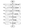
- FIG. 25 is a flowchart for explaining a procedure for updating the offset memory 51 and the gain memory 52. Here, attention is paid to an offset value and a gain value corresponding to one pixel.
- step S310 detection of TFT characteristics based on the first reference voltage Vref1 is performed (step S310).
- step S310 an offset value for correcting the video signal is obtained.
- the offset value obtained in step S310 is stored in the offset value buffer (step S320).
- step S330 the TFT characteristic is detected based on the second reference voltage Vref2 (step S330).
- step S330 a gain value for correcting the video signal is obtained.
- the gain value obtained in step S330 is stored in the gain value buffer (step S340).
- step S350 OLED characteristics are detected during the light emission period Tc (step S350).
- step S350 an offset value and a deterioration correction coefficient for correcting the video signal are obtained.
- step S360 the sum of the offset value stored in the offset value buffer and the offset value obtained in step S350 is stored in the offset memory 51 as a new offset value.
- step S370 the product of the gain value stored in the gain value buffer and the deterioration correction coefficient obtained in step S350 is stored in the gain memory 52 as a new gain value (step S370).
- the offset value and gain value corresponding to one pixel are updated.
- the TFT characteristic and the OLED characteristic are detected for one row in each frame, if noise exceeding the reference value is not detected in all columns, m in the offset memory 51 per frame.
- the offset values and the m gain values in the gain memory 52 are updated.
- the light emission voltage of the organic EL element OLED is measured during the light emission period Tc.
- the greater the detected voltage as the measurement result the greater the degree of deterioration of the organic EL element OLED. Therefore, the offset memory 51 and the gain memory 52 are updated so that the offset value increases and the gain value increases as the detection voltage increases.
- FIG. 26 is a diagram illustrating a configuration of the video signal correction unit.
- the video signal correction unit includes an LUT 211, a multiplication unit 212, and an addition unit 213. In such a configuration, the value of the video signal corresponding to each pixel is corrected as follows.
- gamma correction is performed on the video signal sent from the outside using the LUT 211. That is, the gradation P indicated by the video signal is converted to the control voltage Vc by gamma correction.
- the multiplier 212 receives the control voltage Vc and the gain value B read from the gain memory 52, and outputs a value “Vc ⁇ B” obtained by multiplying them.
- the adder 213 receives the value “Vc ⁇ B” output from the multiplier 212 and the offset value Vt read from the offset memory 51, and outputs the value “Vc ⁇ B + Vt” obtained by adding them. To do.
- the value “Vc ⁇ B + Vt” obtained as described above is sent from the control circuit 20 to the source driver 30 as the data signal DA.
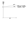
- noise generated in the monitor line M is measured in each frame, and if the magnitude of the noise is less than the reference value for each monitor row, detection of TFT characteristics and OLED characteristics is performed. Then, the video signal sent from the outside is corrected using correction data (offset value and gain value) obtained in consideration of both the detection result of the TFT characteristic and the detection result of the OLED characteristic. Since the data voltage based on the video signal (the data signal DA) corrected in this manner is applied to the data line S, when the organic EL element OLED in each pixel circuit 11 is caused to emit light, A drive current having such a magnitude as to compensate for the deterioration of the organic EL element OLED is supplied to the organic EL element OLED (see FIG. 27).
- the TFT characteristic and the OLED characteristic are not detected, and the correction data is not updated. That is, the correction data is not updated when there is an error that cannot be ignored between the original current value and the measured value with respect to the detected current. Therefore, a reduction in compensation accuracy due to an inappropriate value of correction data is prevented.
- oxide TFTs (specifically, TFTs having an In—Ga—Zn—O-based semiconductor layer) are employed for the transistors T1 to T3 in the pixel circuit 11, so that sufficient S The effect that the / N ratio can be secured is obtained.
- a TFT having an In—Ga—Zn—O-based semiconductor layer is referred to as an “In—Ga—Zn—O—TFT” here.
- In-Ga-Zn-O-TFT and LTPS (Low Temperature-Polysilicon) -TFT are compared, In-Ga-Zn-O-TFT has much smaller off-current than LTPS-TFT.
- the off-current is about 1 pA at maximum.
- the off-current is about 10 fA at maximum. Therefore, for example, the off-current for 1000 rows is about 1 nA at the maximum when LTPS-TFT is employed, and is about 10 pA at the maximum when In—Ga—Zn—O-TFT is employed.
- the detected current is about 10 to 100 nA in any case.
- the monitor line M is connected not only to the pixel circuit 11 in the monitor row but also to the pixel circuit 11 in the non-monitor row.
- the S / N ratio of the monitor line M depends on the total leakage current of the transistors T3 in the non-monitor row. Specifically, the S / N ratio of the monitor line M is represented by “detection current / (leakage current ⁇ number of non-monitor rows)”. From the above, for example, in the organic EL display device having the “Landscape FHD” display unit 10, the S / N ratio is about 10 when the LTPS-TFT is employed, whereas the In— When Ga—Zn—O—TFT is employed, the S / N ratio is about 1000. Thus, in the present embodiment, a sufficient S / N ratio can be ensured when performing current detection.
- the detection of the TFT characteristic and the OLED characteristic is not performed when noise of a reference value or more is detected in the noise measurement period Tn.
- the present invention is not limited to this, and TFT characteristics and OLED characteristics are detected regardless of the magnitude of noise detected during the noise measurement period Tn, and noise exceeding the reference value is detected during the noise measurement period Tn.
- the correction data may not be updated (configuration of this modification).
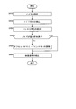
- FIG. 28 is a flowchart for explaining an outline of a driving method when paying attention to a monitor column in a monitor row in the present modification.
- noise generated on the monitor line M is measured (step S410).
- TFT characteristics are detected (step S420).
- OLED characteristics are detected (step S430).
- step S450 is performed after the process of step S450. If the magnitude of the noise is greater than or equal to the reference value, the process of step S450 is performed.
- the process of step S460 is performed without being interrupted.
- step S450 the offset memory 51 and the gain memory 52 are updated using the detection result in step S420 and the detection result in step S430.
- step S460 the correction of the video signal sent from the outside is performed using the correction data stored in the offset memory 51 and the gain memory 52.
- the noise measurement step is realized by step S410
- the characteristic detection step is realized by step S420 and step S430
- the correction data update step is realized by step S450
- the video signal correction step is executed by step S460. It has been realized.
- the first characteristic detection step is realized by step S420
- the second characteristic detection step is realized by step S430.
- FIG. 29 is a diagram for explaining an operation when noise of a reference value or more is detected in a noise measurement period Tn of a certain frame (here, referred to as “target frame”) in the present modification.
- target frame a noise measurement period of a certain frame
- the monitor sequence when noise equal to or higher than the reference value is detected in the noise measurement period Tn of the target frame, correction data update processing based on the result of characteristic detection in the target frame is performed. Not done.
- the present invention has the following features regarding the control of the monitor row.
- characteristic detection immediately after the time when the noise is detected is not performed, or is performed at a time near the time when the noise is detected. Correction data update processing based on characteristic detection is not performed.
- the correction data update process based on the result of the characteristic detection of the target frame is not performed, and the monitor row in the frame two frames after the target frame is the same as the monitor row in the target frame. .
- the noise magnitude is greater than or equal to the reference value in at least one monitor line M, “the noise magnitude is the reference It is assumed that it is determined that “the value is greater than or equal to”.
- FIG. 30 to FIG. 32 are diagrams for explaining the transition of monitor lines in this modification. 30 to 32, the temporal transition of the vertical scanning in the display unit 10 is represented by an arrow 75. Further, it is assumed that the frame starting from time t76 is the first frame and the monitor row of the first frame is the first row.
- the characteristic detection operation for the first row is performed in the first frame, as shown in FIG.
- the second line is the monitor line. If the magnitude of noise detected during the noise measurement period Tn of the first frame is equal to or greater than the reference value, the first line is again set as the monitor line in the second frame as shown in FIG. If the magnitude of noise detected in the noise measurement period Tn of the first frame is less than the reference value and the magnitude of noise detected in the noise measurement period Tn of the second frame is greater than or equal to the reference value, As shown in FIG. 32, the first row is again set as the monitor row in the third frame. At this time, the correction data update process based on the result of the characteristic detection in the first frame is not performed.
- the following operation is performed in this modification.
- the correction data update process based on the result of the characteristic detection in the target frame is not performed, and the Z-th row is also performed in the frame following the target frame Characteristic detection is performed.
- FIG. 33 is a diagram for explaining conditions under which correction data update processing is performed based on the result of characteristic detection in a certain frame (herein referred to as “target frame”) in the present modification.
- the noise detected in the noise measurement period Tn of the target frame is less than the reference value, and the noise of the next frame of the target frame is detected. If the magnitude of noise detected in the measurement period Tn is less than the reference value, correction data update processing based on the result of characteristic detection in the target frame is performed.
- the correction data update process based on the characteristic detection result for the Z-th row is the noise measurement period Tn and the Z-th row immediately before the characteristic detection period for the Z-th row. This is performed only when noise equal to or higher than the reference value is not detected in both the noise measurement period Tn immediately after the characteristic detection period.
- FIG. 34 is a diagram for explaining the operation when noise of a reference value or more is detected in this modification.
- this modification as shown in FIG. 34, regarding the monitor sequence, when noise equal to or higher than the reference value is detected in the noise measurement period Tn of the target frame, correction data update processing based on the result of characteristic detection in the target frame is performed. Not only the correction data update process based on the result of the characteristic detection in the frame before the target frame is not performed.
- FIG. 35 is a flowchart for explaining the outline of the operation in this modification.
- step S510 noise measurement is performed in the frame next to the target frame (step S520).
- step S520 it is assumed that the magnitude of noise detected in the noise measurement period Tn of the target frame is less than the reference value.
- step S520 it is determined whether or not the magnitude of noise measured in step S520 is less than a reference value (step S530).
- step S540 the offset memory 51 and the gain memory 52 are updated using the result of the characteristic detection (characteristic detection in the target frame) in step S510.
- the correction data update process is not performed unless the magnitude of noise is less than the reference value for two frames in succession.
- the result of the characteristic detection in an arbitrary frame is stored in the buffer during a period from when noise measurement is performed in the next frame until correction data update processing is performed.
- the correction data update process is performed only when the magnitude of noise is less than the reference value in both periods before and after the characteristic detection period.
- correction data update processing based on the result of characteristic detection is performed in consideration of the state of noise in the period before and after the characteristic detection period, so that the compensation accuracy is reduced due to an inappropriate value of the correction data Is more effectively prevented.
- the noise measurement period Tn is provided before the characteristic detection period in the frame period, but the present invention is not limited to this.
- a noise measurement period Tn may be provided before and after the characteristic detection period in the frame period.
- the characteristic detection in the corresponding frame is performed only when the noise is less than the reference value in both the noise measurement period Tn in the first half of the frame period and the noise measurement period Tn in the second half of the frame period.
- the correction data update process based on the result may be performed.
- the noise measurement period Tn is provided before the characteristic detection period in the frame period, but the present invention is not limited to this.
- a noise measurement period Tn may be provided after the characteristic detection period in the frame period.
- FIG. 38 when noise of a reference value or more is detected in a noise measurement period Tn of a certain frame (herein referred to as “target frame”) with respect to the monitor sequence, The correction data update process based on the detection result and the correction data update process based on the characteristic detection result in the next frame of the target frame may be prevented from being performed.
- the monitor string as shown in FIG. 39, only when the noise is less than the reference value in both the noise measurement period Tn of the frame preceding the target frame and the noise measurement period Tn of the target frame, Correction data update processing based on the result of characteristic detection may be performed.
- noise is measured in all frames.
- the present invention is not limited to this, and noise may be measured for each of a plurality of frames (configuration of this modification). For example, as shown in FIG. 40, noise may be measured only once every three frames.
- the target frame when noise equal to or higher than a reference value is detected in the noise measurement period Tn of a certain frame (herein referred to as “target frame”), the target is measured after the noise is measured before the target frame.
- the correction data update process based on the result of the characteristic detection performed in the period after the frame until the noise measurement is performed may not be performed.
- the monitor line M is either in a state connected to the current measuring unit 37, a state connected to the voltage measuring unit 38, or a high impedance state, as in the first embodiment.
- the vicinity of one end of the monitor line M has the configuration shown in FIG. That is, one monitor circuit 322 is provided for every K monitor lines M.
- the current does not flow through the monitor line M, the current flows through the organic EL element OLED, and the organic EL element OLED emits light as in the normal operation.
- the above-described characteristic detection operation is performed unless noise above the reference value is detected.
- one monitor circuit 322 is provided for every 100 monitor lines M. It ’s fine.
- the compensation accuracy is reduced due to noise while suppressing the increase in the circuit area. It becomes possible to prevent.
- the OLED characteristic is detected by measuring the voltage of the anode of the organic EL element OLED in a state where a constant current is applied to the organic EL element OLED.
- the present invention is not limited to this, and the configuration in which the OLED characteristic is detected by measuring the current flowing through the organic EL element OLED in a state where a constant voltage is applied to the organic EL element OLED (in this modification example). Configuration).
- both the TFT characteristic detection and the OLED characteristic detection are performed by measuring the current. For this reason, as shown in FIG. 42, the component for measuring the voltage is not provided in the monitor circuit 323.
- the monitor line M (j) is in either a state connected to the current measurement unit 39 or a high impedance state based on the switching control signal SW.
- FIG. 43 is a diagram showing a detailed configuration of the current measurement unit 39 in the present modification.
- the current measurement unit 39 includes an operational amplifier 391, a capacitor 392, a first switch 393, a second switch 394, an offset / amplification rate adjustment unit 395, and an A / D converter 396.
- the operational amplifier 391 the non-inverting input terminal is connected to the second switch 394, and the inverting input terminal is connected to the monitor line M.
- the capacitor 392 and the first switch 393 are provided between the output terminal of the operational amplifier 391 and the monitor line M.
- the offset / amplification rate adjustment unit 395 is provided between the output terminal of the operational amplifier 391 and the A / D converter 396.
- the second switch 394 functions as a switch for switching the potential of the non-inverting input terminal of the operational amplifier 391 between the potential of the low-level power supply line ELVSS and the potential Vel for detecting OLED characteristics.
- the current measuring unit 39 is configured by an integrating circuit.
- the potential Vel for detecting the OLED characteristic is “the difference between the offset value stored in the offset memory 51 and the offset value obtained in the TFT characteristic detection period Ta” and “the gain value stored in the gain memory 52. And a gain value obtained during the TFT characteristic detection period Ta, the potential corresponding to the sum of the “equivalent voltage corresponding to the emission voltage”.
- the potential of the non-inverting input terminal of the operational amplifier 391 is set to the low level power supply line ELVSS by the second control clock signal Sclk2.
- the operation similar to that of the first embodiment is performed in the state of being set to the potential.
- the potential of the non-inverting input terminal of the operational amplifier 391 is set to the potential Vel for detecting the OLED characteristic by the second control clock signal Sclk2.
- the first switch 393 is turned on by the control clock signal Sclk1.
- the output terminal and the inverting input terminal of the operational amplifier 391 are short-circuited, and the potential of the monitor line M becomes equal to the potential Vel for detecting OLED characteristics.
- the first switch 393 is turned off by the first control clock signal Sclk1.
- the potential of the output terminal of the operational amplifier 391 changes according to the magnitude of the current flowing through the monitor line M (source current supplied to the organic EL element OLED).
- the change in the potential is reflected in the digital signal output from the A / D converter 396.
- the digital signal is output from the monitor circuit 323 as monitor data MO.
- the offset / amplification rate adjustment unit 395 has a function of making the input level to the A / D converter 396 the same when detecting TFT characteristics and when detecting OLED characteristics.
- FIG. 44 is a timing chart for explaining the operation of the pixel circuit 11 (referred to as the pixel circuit 11 of i rows and j columns) included in the monitor column of the monitor rows in the present modification.
- the magnitude of noise detected during the noise measurement period Tn is less than the reference value.
- the constant voltage V (i, j) is applied to the monitor line M during the period for detecting the OLED characteristic in the light emission period Tc. Is given in (j).
- the OLED characteristic is detected by measuring the current flowing through the organic EL element OLED in a state where a constant voltage is applied to the organic EL element OLED as described above. Thereby, the measurement time can be shortened.
- the magnitude of the constant voltage applied to the organic EL element OLED is based on a deterioration correction coefficient obtained from the difference between the gain value stored in the gain memory 52 and the gain value obtained in the TFT characteristic detection period Ta. It is good to ask. Further, when detecting the OLED characteristics, it is preferable to adjust the length of time for applying a constant voltage to the organic EL element OLED according to the target luminance. Further, if the integrated value of the light emission current in one frame period becomes a value corresponding to a desired gradation, the voltage value is changed during the light emission period Tc, and the characteristics (current-voltage) at a plurality of operating points are changed. (Characteristic) may be measured.
- FIG. 45 is a block diagram showing an overall configuration of an active matrix organic EL display device 2 according to the second embodiment of the present invention. As shown in FIG. 45, the organic EL display device 2 according to the present embodiment is provided with a touch panel 80 in addition to the components in the first embodiment.
- the touch panel is relatively easy to generate noise. For this reason, in an organic EL display device equipped with a touch panel, the touch panel is often clocked during a vertical blanking period. Therefore, also in this embodiment, it is assumed that the touch panel 80 performs a clock operation during the vertical blanking period.
- the control unit controls the pixel circuit driving unit (the source driver 30 and the source driver 30) so that the characteristic detection operation is not performed through the vertical blanking period (period in which the clock operation by the touch panel 80 is performed).
- the operation of the gate driver 40 is controlled.
- FIG. 46 is a timing chart for explaining the operation of the pixel circuit 11 (referred to as the pixel circuit 11 of i rows and j columns) included in the monitor column of the monitor rows in the present embodiment.
- the vertical blanking period is represented by the symbol Tf.
- the characteristic detection operation is stopped during the vertical blanking period Tf. That is, the process of measuring the magnitude of the current flowing through the monitor line M is stopped during the vertical blanking period Tf.
- size of a desired electric current by repeating the measurement of current before and behind the vertical blanking period Tf, and performing the averaging process of a measurement result.
- FIG. 47 is a block diagram showing the overall configuration of an active matrix organic EL display device 3 according to the third embodiment of the present invention.
- a noise monitor circuit 85 for detecting noise is provided outside the organic EL panel.
- the current measurement for obtaining the TFT characteristics and the voltage measurement for obtaining the OLED characteristics are performed by the monitor circuit 322, and the noise measurement is performed by the noise monitor circuit 85.
- the noise measurement unit is realized by the noise monitor circuit 85. That is, the noise measurement unit is provided outside the organic EL panel separately from the characteristic detection unit (monitor circuit 322).
- FIG. 48 is a flowchart for explaining the control algorithm.
- FIG. 49 is a diagram for explaining each control.
- the control circuit 20 controls the operations of the source driver 30 and the gate driver 40 based on this control algorithm.
- a procedure for determining a control method for data to be processed data indicating rows, columns, and gradations (hereinafter referred to as “target data”) will be described with reference to FIG.
- step S610 it is determined whether or not the magnitude of noise detected by the noise monitor circuit 85 is less than a reference value. If the magnitude of the noise is greater than or equal to the reference value, the control method for the target data is “control E”. If the magnitude of the noise is less than the reference value, the determination at step S620 is further performed. In step S620, it is determined whether the target data is monitor row data. If the target data is not the monitor row data, the control method for the target data is “control A1”. If the target data is monitor row data, the determination in step S630 is further performed. In step S630, it is determined whether the target data is monitor row data. If the target data is not data in the monitor row, the control method for the target data is “control B”.
- step S640 it is determined whether the target data is low gradation data (gradation data for displaying black or gradation data for displaying substantially black). If the target data is not low gradation data, the control method for the target data is “control C”. If the target data is low gradation data, the control method for the target data is “control D”.
- control A1 “control B”, “control C”, and “control D” are the same as those in the first embodiment, description thereof is omitted.
- Control E is a control method for each data when noise above the reference value is detected. Since noise equal to or higher than the reference value is detected and it is not necessary to perform characteristic detection, the scanning line G1 (i) is in an active state (high level state) only for one normal horizontal scanning period. The monitor control line G2 (i) is in an inactive state (low level state) in all rows. In order to perform the characteristic detection operation from the corresponding row after the next frame, the row in the active state is stored immediately before deactivating the monitor control lines G2 (i) in all rows. In addition, since it is only necessary to perform normal display, a data voltage corresponding to normal gradation data is applied to the data line S (j). Since it is not necessary to perform characteristic detection, the monitor line switch 331 is turned off. Since the characteristic detection is not performed, the correction data is not updated.
- a circuit for measuring noise is provided separately from the monitor circuit 322 for detecting the TFT characteristics and the OLED characteristics.
- Noise can be measured at any timing. That is, an arbitrary period in the frame period can be set as the noise measurement period Tn.
- any period such as a period indicated by reference numeral Tn1, a period indicated by reference numeral Tn2, a period indicated by reference numeral Tn3, a period indicated by reference numeral Tn4, and a period indicated by reference numeral Tn5 may be used as the noise measurement period.
- the organic EL display device to which the present invention is applicable is not limited to the one provided with the pixel circuit 11 shown in FIG.
- the pixel circuit may have a configuration other than that shown in FIG. 7 as long as it includes at least an electro-optical element (organic EL element OLED) controlled by current, transistors T1 to T3, and a capacitor Cst.
- 1 to 8 show modifications of the first embodiment. These first to eighth modifications can be applied to the second embodiment and the third embodiment. Further, the first to eighth modifications can be appropriately combined and employed. For example, the first modification and the seventh modification may be applied to the first embodiment.
- both TFT characteristics and OLED characteristics are detected in each frame, but the present invention is not limited to this.
- the present invention can be applied as long as at least one of the TFT characteristic and the OLED characteristic is detected during the characteristic detection period of each frame.
Landscapes
- Engineering & Computer Science (AREA)
- Physics & Mathematics (AREA)
- Computer Hardware Design (AREA)
- General Physics & Mathematics (AREA)
- Theoretical Computer Science (AREA)
- Control Of Indicators Other Than Cathode Ray Tubes (AREA)
- Electroluminescent Light Sources (AREA)
- Control Of El Displays (AREA)
Abstract
Description
ノイズを測定するノイズ測定ステップと、
前記駆動トランジスタおよび前記電気光学素子の少なくとも一方の特性を検出する特性検出ステップと、
前記表示装置に設けられた補正データ記憶部に記憶されている補正データを前記特性検出ステップでの検出結果に基づいて更新する補正データ更新ステップと、
前記n×m個の画素回路に供給するための映像信号を前記補正データ記憶部に記憶されている補正データに基づいて補正する映像信号補正ステップと
を含み、
前記ノイズ測定ステップで基準値以上のノイズが検出されたとき、当該ノイズが検出された時点の直後における前記特性検出ステップの処理が行われない、または、当該ノイズが検出された時点の近傍の時点に行われた前記特性検出ステップでの検出結果に基づく前記補正データ更新ステップの処理が行われないことを特徴とする。
前記ノイズ測定ステップで前記基準値以上のノイズが検出されたとき、当該ノイズが検出された時点の直前に行われた前記特性検出ステップでの検出結果に基づく前記補正データ更新ステップの処理および当該ノイズが検出された時点の直後に行われた前記特性検出ステップでの検出結果に基づく前記補正データ更新ステップの処理の少なくとも一方が行われないことを特徴とする。
フレーム期間において、前記特性検出ステップでは、前記画素マトリクスの1つの行のみについて前記駆動トランジスタおよび前記電気光学素子の少なくとも一方の特性が検出され、
Z行目(Zは1以上n以下の整数)についての前記特性検出ステップの処理が行われたフレーム期間のことを対象フレーム期間と定義したとき、
前記対象フレーム期間において前記ノイズ測定ステップで前記基準値以上のノイズが検出された場合には、前記対象フレーム期間に行われた前記特性検出ステップでの検出結果に基づく前記補正データ更新ステップの処理は行われず、前記対象フレーム期間の次のフレーム期間においてもZ行目についての前記特性検出ステップの処理が行われ、
前記対象フレーム期間において前記ノイズ測定ステップで前記基準値以上のノイズが検出されず、かつ、前記対象フレーム期間の次のフレーム期間において前記ノイズ測定ステップで前記基準値以上のノイズが検出された場合には、前記対象フレーム期間に行われた前記特性検出ステップでの検出結果に基づく前記補正データ更新ステップの処理および前記対象フレーム期間の次のフレーム期間に行われた前記特性検出ステップでの検出結果に基づく前記補正データ更新ステップの処理は行われず、前記対象フレーム期間の2フレーム後のフレーム期間においてもZ行目についての前記特性検出ステップの処理が行われることを特徴とする。
フレーム期間において、前記特性検出ステップでは、前記画素マトリクスの1つの行のみについて前記駆動トランジスタおよび前記電気光学素子の少なくとも一方の特性が検出され、
Z行目(Zは1以上n以下の整数)についての前記特性検出ステップでの検出結果に基づく前記補正データ更新ステップの処理は、Z行目についての前記特性検出ステップの直前に行われた前記ノイズ測定ステップおよびZ行目についての前記特性検出ステップの直後に行われた前記ノイズ測定ステップの双方で前記基準値以上のノイズが検出されなかったときのみ行われることを特徴とする。
フレーム期間において、前記特性検出ステップの前後に前記ノイズ測定ステップの処理が行われることを特徴とする。
複数のフレーム期間毎に前記ノイズ測定ステップの処理が行われることを特徴とする。
前記特性検出ステップは、
前記駆動トランジスタの特性を検出する第1の特性検出ステップと、
前記電気光学素子の特性を検出する第2の特性検出ステップと
を含み、
1フレーム期間は、前記ノイズ測定ステップの処理が行われるノイズ測定期間と、前記電気光学素子を発光させる準備が行われる選択期間と、前記電気光学素子の発光が行われる発光期間とを含み、
前記第1の特性検出ステップの処理は、前記選択期間に行われ、
前記第2の特性検出ステップの処理は、前記発光期間に行われることを特徴とする。
前記第2の特性検出ステップでは、前記電気光学素子に一定の電流が与えられた状態で前記電気光学素子の陽極の電圧を測定することによって、前記電気光学素子の特性が検出されることを特徴とする。
前記第2の特性検出ステップでは、前記電気光学素子に一定の電圧が与えられた状態で前記電気光学素子に流れる電流を測定することによって、前記電気光学素子の特性が検出されることを特徴とする。
前記第1の特性検出ステップでは、前記駆動トランジスタのゲート-ソース間の電圧を所定の大きさにした状態で前記駆動トランジスタのドレイン-ソース間を流れる電流を測定することによって、前記駆動トランジスタの特性が検出されることを特徴とする。
前記表示装置は、タッチパネルを更に有し、
前記タッチパネルによるクロック動作が行われる期間を通じて前記特性検出ステップの処理が行われないことを特徴とする。
前記タッチパネルは、垂直帰線期間中にクロック動作を行い、
垂直帰線期間を通じて前記特性検出ステップの処理が行われないことを特徴とする。
前記駆動トランジスタおよび前記電気光学素子の少なくとも一方の特性を検出する特性検出処理を行いつつ前記n×m個の画素回路を駆動する画素回路駆動部と、
映像信号を補正するための補正データが記憶される補正データ記憶部と、
前記補正データ記憶部に記憶されている補正データを前記特性検出処理での検出結果に基づいて更新する補正データ更新処理および前記n×m個の画素回路に供給するための映像信号を前記補正データ記憶部に記憶されている補正データに基づいて補正する映像信号補正処理を行いつつ前記画素回路駆動部の動作を制御する制御部と、
ノイズを測定するノイズ測定部と
を備え、
前記制御部は、前記ノイズ測定部によって基準値以上のノイズが検出されたとき、当該ノイズが検出された時点の直後における前記特性検出処理が行われないよう前記画素回路駆動部の動作を制御する、または、当該ノイズが検出された時点の近傍の時点に行われた前記特性検出処理での検出結果に基づく前記補正データ更新処理を行わないことを特徴とする。
前記制御部は、前記ノイズ測定部によって前記基準値以上のノイズが検出されたとき、当該ノイズが検出された時点の直前に行われた前記特性検出処理での検出結果に基づく前記補正データ更新処理および当該ノイズが検出された時点の直後に行われた前記特性検出処理での検出結果に基づく前記補正データ更新処理の少なくとも一方を行わないことを特徴とする。
前記画素マトリクスの各列に対応するように設けられたモニタ線を更に備え、
前記画素回路駆動部は、前記モニタ線を流れる電流または前記モニタ線上の所定の位置の電圧を測定することによって前記特性検出処理を行う特性検出部を含むことを特徴とする。
前記ノイズ測定部は、前記特性検出部と同じ回路を共有し、
前記ノイズ測定部によるノイズの測定が行われるときには、前記モニタ線は前記電気光学素子および前記駆動トランジスタとは電気的に切り離された状態にされることを特徴とする。
前記ノイズ測定部は、前記特性検出部とは別に、前記画素マトリクスを含む有機ELパネルの外部に設けられていることを特徴とする。
前記特性検出部は、K本のモニタ線(Kは2以上m以下の整数)につき1つだけ設けられ、
フレーム期間において、
前記K本のモニタ線のうちの1つが前記特性検出部と電気的に接続され、
前記特性検出部と電気的に接続されていないモニタ線は、ハイインピーダンスの状態にされていることを特徴とする。
タッチパネルを更に備え、
前記制御部は、前記タッチパネルによるクロック動作が行われる期間を通じて前記特性検出処理が停止するよう、前記画素回路駆動部の動作を制御することを特徴とする。
前記タッチパネルは、垂直帰線期間中にクロック動作を行い、
前記制御部は、垂直帰線期間を通じて前記特性検出処理が停止するよう、前記画素回路駆動部の動作を制御することを特徴とする。
<1.1 全体構成>
図2は、本発明の第1の実施形態に係るアクティブマトリクス型の有機EL表示装置1の全体構成を示すブロック図である。この有機EL表示装置1は、表示部(有機ELパネル)10,コントロール回路20,ソースドライバ(データ線駆動回路)30,ゲートドライバ(走査線駆動回路)40,オフセットメモリ51,およびゲインメモリ52を備えている。なお、ソースドライバ30およびゲートドライバ40の一方または双方が表示部10と一体的に形成された構成であっても良い。また、オフセットメモリ51とゲインメモリ52とは物理的には1つのメモリで構成されていても良い。
<1.2.1 画素回路>
図7は、画素回路11およびモニタ回路322の構成を示す図である。なお、図7に示す画素回路11は、i行j列の画素回路11である。この画素回路11は、1個の有機EL素子OLED,3個のトランジスタT1~T3,および1個のコンデンサCstを備えている。トランジスタT1は画素を選択する入力トランジスタとして機能し、トランジスタT2は有機EL素子OLEDへの電流の供給を制御する駆動トランジスタとして機能し、トランジスタT3はTFT特性やOLED特性を検出するか否かを制御するモニタ制御トランジスタとして機能する。
本実施形態においては、画素回路11内のトランジスタT1~T3はすべてnチャネル型である。また、本実施形態においては、トランジスタT1~T3には、酸化物TFT(酸化物半導体をチャネル層に用いた薄膜トランジスタ)が採用されている。
図7に示すように、モニタ回路322には、電流測定部37と電圧測定部38とが含まれている。なお、本実施形態においては、このモニタ回路322によって、特性検出部とノイズ測定部とが実現されている。換言すれば、ノイズ測定部は、特性検出部と同じ回路を共有している。電流測定部37および電圧測定部38とモニタ線M(j)との関係は、コントロール回路20から出力回路330に与えられる切替制御信号SWに基づいて制御される。その切替制御信号SWに基づいて、出力回路330内に設けられているスイッチ(以下、「モニタラインスイッチ」という。)331は、モニタ線M(j)を、電流測定部37に接続された状態または電圧測定部38に接続された状態またはハイインピーダンスの状態のいずれかとする。なお、図7では、出力回路330については一部の構成のみを示している。
<1.3.1 概要>
次に、本実施形態における駆動方法について説明する。上述したように、本説明においては、任意のフレームに着目したときに通常よりも長い選択期間が設けられている行のことを「モニタ行」という。また、本実施形態においては、モニタ行のうちのQ列(Qは1以上m以下の整数)が、TFT特性およびOLED特性の検出対象の列となる。本説明においては、TFT特性およびOLED特性の検出対象の列のことを「モニタ列」といい、モニタ列以外の列のことを「非モニタ列」という。
次に、ノイズ測定と特性検出(TFT特性およびOLED特性の検出)と補正データ更新処理(特性検出の結果を用いてオフセットメモリ51およびゲインメモリ52を更新する処理)との関係について説明する。本実施形態においては、モニタ行に着目すると、図11に示すように、1フレーム期間の最初にノイズ測定期間が設けられ、ノイズ測定期間の後に特性検出期間が設けられている。ノイズ測定期間には、モニタ線Mに生じたノイズの測定が行われる。特性検出期間には、モニタ行において上述した特性検出動作が行われる。
<1.3.3.1 通常動作>
各フレームにおいて、非モニタ行では、通常動作が行われる。非モニタ行に含まれる画素回路11では、目標輝度に対応するデータ電圧に基づく書き込みが選択期間に行われた後、トランジスタT1はオフ状態で維持される。データ電圧に基づく書き込みによってトランジスタT2はオン状態となる。トランジスタT3についてはオフ状態で維持される。以上より、図14で符号70で示す矢印のように、トランジスタT2を介して有機EL素子OLEDに駆動電流が供給される。これにより、駆動電流に応じた輝度で有機EL素子OLEDが発光する。
各フレームにおいて、モニタ行で特性検出動作が行われる直前に、モニタ線Mに生じたノイズの測定が行われる。そして、本実施形態においては、ノイズの大きさが基準値未満であるモニタ列でのみ、特性検出動作が行われる。
次に、本実施形態における制御アルゴリズムについて説明する。図23は、制御アルゴリズムを説明するためのフローチャートである。図24は、各制御の説明をするための図である。コントロール回路20は、この制御アルゴリズムに基づいて、ソースドライバ30およびゲートドライバ40の動作を制御する。まず、図23を参照しつつ、処理対象のデータ(行,列,および階調を示すデータ)(以下、「対象データ」という。)に対する制御方法の決定手順について説明する。
“制御A1”は、非モニタ行のデータに対する制御方法である。特性検出を行う必要がないので、走査線G1(i)については通常の1水平走査期間だけアクティブな状態(ハイレベルの状態)とされ、モニタ制御線G2(i)については前状態が維持される。また、通常通りの表示が行われれば良いので、データ線S(j)には通常の階調データに対応するデータ電圧が印加される。ノイズ測定後のモニタラインスイッチ331の状態については前状態が維持される。特性検出は行われないので、補正データの更新は行われない。
“制御A2”は、モニタ行のデータのうちノイズ測定期間Tnに基準値以上のノイズが検出されたモニタ列のデータに対する制御方法である。対象データはモニタ行のデータであるので、走査線G1(i)については、通常の1水平走査期間とTFT特性検出期間Taとの合計の期間、アクティブな状態とされる。モニタ制御線G2(i)については前状態が維持される。また、通常通りの表示が行われれば良いので、データ線S(j)には通常の階調データに対応するデータ電圧が印加される。ノイズ測定後のモニタラインスイッチ331の状態については前状態が維持される。特性検出は行われないので、補正データの更新は行われない。
“制御B”は、モニタ行のデータのうちの非モニタ列のデータに対する制御方法である。対象データはモニタ行のデータであるので、走査線G1(i)については、通常の1水平走査期間とTFT特性検出期間Taとの合計の期間、アクティブな状態とされる。また、モニタ行に対応するモニタ制御線G2(i)が、TFT特性検出期間Taおよび発光期間Tcにアクティブな状態とされる。しかしながら、対象データは非モニタ列のデータであって、特性検出を行う必要がないので、ノイズ測定後のモニタラインスイッチ331の状態はオフ状態とされる(モニタ線M(j)がハイインピーダンスにされた状態とされる)。データ線S(j)には通常の階調データに補正係数k(kは1近傍の値)を乗じたデータに対応するデータ電圧が印加される。補正係数kが設けられている理由は、トランジスタT3がオン状態となっているためモニタ線M(j)の配線容量によっては本来よりもデータ電圧を大きくする必要があるからである。特性検出は行われないので、補正データの更新は行われない。
“制御C”は、特性検出が行われるべきデータのうちの低階調データ以外のデータに対する制御方法である。対象データは特性検出が行われるべきデータであるので、走査線G1(i)については、通常の1水平走査期間とTFT特性検出期間Taとの合計の期間、アクティブな状態とされる。また、モニタ行に対応するモニタ制御線G2(i)が、TFT特性検出期間Taおよび発光期間Tcにアクティブな状態とされる。データ線S(j)には、トランジスタT2をオフ状態にするために黒書込期間Tbに黒色表示に相当する電圧が印加される。特性検出を行う必要があるので、ノイズ測定後のモニタラインスイッチ331の状態はオン状態とされる(モニタ線M(j)が電流測定部37または電圧測定部38に接続された状態とされる)。モニタ線M(j)には、TFT特性を検出するためにローレベル電源電圧ELVSSが供給された後、有機EL素子OLEDを発光させつつOLED特性を検出するために階調信号が供給される。TFT特性およびOLED特性の検出が行われるので、補正データの更新は行われる。
“制御D”は、特性検出が行われるべきデータのうちの低階調データに対する制御方法である。対象データは特性検出が行われるべきデータであるので、走査線G1(i)については、通常の1水平走査期間とTFT特性検出期間Taとの合計の期間、アクティブな状態とされる。また、モニタ行に対応するモニタ制御線G2(i)が、TFT特性検出期間Taおよび発光期間Tcにアクティブな状態とされる。データ線S(j)には、トランジスタT2をオフ状態にするために黒書込期間Tbに黒色表示に相当する電圧が印加される。特性検出を行う必要があるので、ノイズ測定後のモニタラインスイッチ331の状態はオン状態とされる(モニタ線M(j)が電流測定部37または電圧測定部38に接続された状態とされる)。モニタ線M(j)には、TFT特性を検出するためにローレベル電源電圧ELVSSが供給される。なお、低階調データについては、不必要な発光を防止するため、有機EL素子OLEDを発光させるための階調信号のモニタ線M(j)への供給は行われない。TFT特性の検出が行われるので、補正データの更新は行われる。但し、更新されるデータは、TFT特性に関するデータのみである。
次に、オフセットメモリ51に格納されているオフセット値およびゲインメモリ52に格納されているゲイン値がどのように更新されるかについて説明する。なお、ノイズ測定期間Tnに検出されたノイズが基準値未満であって特性検出動作が行われた画素のデータについてのみ、オフセット値およびゲイン値の更新が行われる。図25は、オフセットメモリ51およびゲインメモリ52の更新の手順を説明するためのフローチャートである。なお、ここでは1つの画素に対応するオフセット値およびゲイン値に着目する。
本実施形態においては、駆動トランジスタの劣化および有機EL素子OLEDの劣化を補償するために、オフセットメモリ51およびゲインメモリ52に格納されている補正データを用いて、外部から送られる映像信号の補正が行われる。以下、映像信号のこの補正について説明する。
本実施形態によれば、各フレームにおいて、モニタ線Mに生じるノイズの測定が行われ、各モニタ列について、ノイズの大きさが基準値未満であればTFT特性およびOLED特性の検出が行われる。そして、TFT特性の検出結果およびOLED特性の検出結果の双方を考慮して求められた補正データ(オフセット値およびゲイン値)を用いて、外部から送られる映像信号が補正される。このようにして補正された映像信号(上記データ信号DA)に基づくデータ電圧がデータ線Sに印加されるので、各画素回路11内の有機EL素子OLEDを発光させる際に、駆動トランジスタの劣化および有機EL素子OLEDの劣化が補償されるような大きさの駆動電流が有機EL素子OLEDに供給される(図27参照)。ここで、ノイズの大きさが基準値以上であれば、TFT特性およびOLED特性の検出は行われず、補正データの更新は行われない。すなわち、検出電流に関して本来の電流値と測定値との間に無視することのできない程度の誤差が生じているような時には、補正データは更新されない。従って、補正データの値が不適切な値となることによる補償精度の低下が防止される。以上のように、本実施形態によれば、回路素子の劣化を補償するために外部補償技術が採用されている有機EL表示装置において、ノイズに起因する補償精度の低下を防止することが可能となる。
以下、上記第1の実施形態の変形例について説明する。なお、以下においては、第1の実施形態と異なる点についてのみ詳しく説明し、第1の実施形態と同様の点については説明を省略する。
上記第1の実施形態においては、モニタ列に関し、ノイズ測定期間Tnに基準値以上のノイズが検出された場合にはTFT特性およびOLED特性の検出が行われなかった。しかしながら、本発明はこれに限定されず、ノイズ測定期間Tnに検出されたノイズの大きさに関わらずTFT特性およびOLED特性の検出を行い、ノイズ測定期間Tnに基準値以上のノイズが検出された場合には補正データの更新を行わないようにしても良い(本変形例の構成)。
フレームが替わる毎に必ずモニタ行も替える構成にした場合、行によりTFT特性およびOLED特性の検出回数に差が生じ得る。そこで、本変形例においては、或るフレーム(ここでは「対象フレーム」という。)のノイズ測定期間Tnに基準値以上のノイズが検出された場合、対象フレームの次のフレームにおけるモニタ行と対象フレームにおけるモニタ行とが同じ行とされる。また、本変形例においては、対象フレームのノイズ測定期間Tnに検出されたノイズの大きさが基準値未満であって、対象フレームの次のフレームのノイズ測定期間Tnに検出されたノイズの大きさが基準値以上であった場合、対象フレームの特性検出の結果に基づく補正データ更新処理は行われず、対象フレームの2フレーム後のフレームにおけるモニタ行と対象フレームにおけるモニタ行とが同じ行とされる。なお、以上のような制御を列毎に行うことはできないので、本変形例においては、少なくとも1つのモニタ線Mでノイズの大きさが基準値以上であった場合に「ノイズの大きさは基準値以上である」と判断されるものと仮定する。
上記第1の実施形態においては、或るフレーム(ここでは「対象フレーム」という。)のノイズ測定期間Tnに検出されたノイズの大きさが基準値未満であれば、対象フレームの次のフレームのノイズ測定期間Tnに検出されるノイズの大きさに関わらず、対象フレームにおける特性検出の結果に基づく補正データ更新処理が行われていた。しかしながら、本発明はこれに限定されず、対象フレームおよび対象フレームの次のフレームの双方でノイズ測定期間Tnに検出されたノイズの大きさが基準値未満であった場合にのみ対象フレームにおける特性検出の結果に基づく補正データ更新処理が行われるようにしても良い(本変形例の構成)。
上記第1の実施形態では、フレーム期間において特性検出期間よりも前にノイズ測定期間Tnが設けられていたが、本発明はこれに限定されない。図36に示すように、フレーム期間において特性検出期間の前後にノイズ測定期間Tnが設けられていても良い。この例の場合、モニタ列に関し、フレーム期間の前半のノイズ測定期間Tnおよびフレーム期間の後半のノイズ測定期間Tnの双方でノイズが基準値未満であった場合にのみ、該当するフレームにおける特性検出の結果に基づく補正データ更新処理が行われるようにすれば良い。
上記第1の実施形態では、フレーム期間において特性検出期間よりも前にノイズ測定期間Tnが設けられていたが、本発明はこれに限定されない。図37に示すように、フレーム期間において特性検出期間よりも後にノイズ測定期間Tnが設けられていても良い。この例の場合、モニタ列に関し、図38に示すように、或るフレーム(ここでは「対象フレーム」という。)のノイズ測定期間Tnに基準値以上のノイズが検出されると、対象フレームにおける特性検出の結果に基づく補正データ更新処理および対象フレームの次のフレームにおける特性検出の結果に基づく補正データ更新処理が行われないようにすれば良い。また、モニタ列に関し、図39に示すように、対象フレームの前のフレームのノイズ測定期間Tnおよび対象フレームのノイズ測定期間Tnの双方でノイズが基準値未満であった場合にのみ、対象フレームにおける特性検出の結果に基づく補正データ更新処理が行われるようにすれば良い。
上記第1の実施形態においては、全てのフレームでノイズの測定が行われていた。しかしながら、本発明はこれに限定されず、複数フレーム毎にノイズの測定が行われるようにしても良い(本変形例の構成)。例えば、図40に示すように、3フレームにつき1回だけノイズの測定が行われるようにしても良い。
上記第1の実施形態においては、1つの列につき1つのモニタ回路322が設けられていることを前提に説明していた。しかしながら、本発明はこれに限定されず、1つのモニタ回路322を複数の列で共有化する構成(本変形例の構成)を採用することもできる。
上記第1の実施形態においては、有機EL素子OLEDに一定の電流が与えられた状態で有機EL素子OLEDの陽極の電圧を測定することによってOLED特性の検出が行われていた。しかしながら、本発明はこれに限定されず、有機EL素子OLEDに一定の電圧が与えられた状態で有機EL素子OLEDに流れる電流を測定することによってOLED特性の検出が行われる構成(本変形例の構成)であっても良い。
<2.1 構成>
図45は、本発明の第2の実施形態に係るアクティブマトリクス型の有機EL表示装置2の全体構成を示すブロック図である。図45に示すように、本実施形態に係る有機EL表示装置2には、上記第1の実施形態における構成要素に加えて、タッチパネル80が設けられている。
タッチパネルを搭載した有機EL表示装置においては、仮に特性検出期間の前後のノイズ測定期間Tnに基準値以上のノイズが検出されなかったとしても、当該特性検出期間に例えばTFT特性を求めるための電流がタッチパネルのクロック動作に起因して正しく検出されないことがあり得る。そこで、本実施形態においては、垂直帰線期間(タッチパネル80によるクロック動作が行われる期間)を通じて特性検出動作が行われないよう、制御部(コントロール回路20)が画素回路駆動部(ソースドライバ30およびゲートドライバ40)の動作を制御する。
本実施形態によれば、回路素子の劣化を補償するために外部補償技術が採用されている有機EL表示装置において、タッチパネルが搭載されていても、ノイズに起因する補償精度の低下を防止することが可能となる。
<3.1 構成>
図47は、本発明の第3の実施形態に係るアクティブマトリクス型の有機EL表示装置3の全体構成を示すブロック図である。本実施形態においては、ノイズを検出するためのノイズモニタ回路85が有機ELパネルの外部に設けられている。このような構成において、TFT特性を求めるための電流の測定およびOLED特性を求めるための電圧の測定はモニタ回路322で行われ、ノイズの測定はノイズモニタ回路85で行われる。このようにノイズの測定は有機ELパネルの外部で行われるため、列毎にノイズの大きさの判断が行われるのではない。なお、本実施形態においては、ノイズモニタ回路85によってノイズ測定部が実現されている。すなわち、ノイズ測定部は、特性検出部(モニタ回路322)とは別に、有機ELパネルの外部に設けられている。
次に、本実施形態における制御アルゴリズムについて説明する。なお、ここでは、特性検出動作が行われる前にノイズモニタ回路85でノイズの測定が行われるものと仮定する。図48は、制御アルゴリズムを説明するためのフローチャートである。図49は、各制御の説明をするための図である。コントロール回路20は、この制御アルゴリズムに基づいて、ソースドライバ30およびゲートドライバ40の動作を制御する。まず、図48を参照しつつ、処理対象のデータ(行,列,および階調を示すデータ)(以下、「対象データ」という。)に対する制御方法の決定手順について説明する。
本実施形態によれば、ノイズを測定するための回路(ノイズモニタ回路85)がTFT特性の検出やOLED特性の検出を行うためのモニタ回路322とは別に設けられているので、フレーム期間中の任意のタイミングでノイズの測定を行うことが可能となる。すなわち、フレーム期間中の任意の期間をノイズ測定期間Tnとすることができる。例えば、図50において符号Tn1で示す期間,符号Tn2で示す期間,符号Tn3で示す期間,符号Tn4で示す期間,符号Tn5で示す期間など、いずれの期間をノイズ測定期間としても良い。
本発明を適用可能な有機EL表示装置は、図7に示した画素回路11を備えるものに限定されるものではない。画素回路は、少なくとも、電流によって制御される電気光学素子(有機EL素子OLED),トランジスタT1~T3,およびコンデンサCstを備えていれば、図7に示した構成以外の構成であっても良い。
10…表示部
11…画素回路
20…コントロール回路
30…ソースドライバ
31…駆動信号発生回路
32…信号変換回路
33…出力部
37,39…電流測定部
38…電圧測定部
40…ゲートドライバ
51…オフセットメモリ
52…ゲインメモリ
80…タッチパネル
85…ノイズモニタ回路
321…階調信号発生回路
322,323…モニタ回路
330…出力回路
T1~T3…トランジスタ
Cst…コンデンサ
G1(1)~G1(n)…走査線
G2(1)~G2(n)…モニタ制御線
S(1)~S(m)…データ線
M(1)~M(m)…モニタ線
Ta…TFT特性検出期間
Tb…黒書込期間
Tc…発光期間
Tn…ノイズ測定期間
Claims (20)
- 電流によって輝度が制御される電気光学素子および前記電気光学素子に供給すべき電流を制御するための駆動トランジスタをそれぞれが含むn×m個(nおよびmは2以上の整数)の画素回路からなるn行×m列の画素マトリクスを有する表示装置の駆動方法であって、
ノイズを測定するノイズ測定ステップと、
前記駆動トランジスタおよび前記電気光学素子の少なくとも一方の特性を検出する特性検出ステップと、
前記表示装置に設けられた補正データ記憶部に記憶されている補正データを前記特性検出ステップでの検出結果に基づいて更新する補正データ更新ステップと、
前記n×m個の画素回路に供給するための映像信号を前記補正データ記憶部に記憶されている補正データに基づいて補正する映像信号補正ステップと
を含み、
前記ノイズ測定ステップで基準値以上のノイズが検出されたとき、当該ノイズが検出された時点の直後における前記特性検出ステップの処理が行われない、または、当該ノイズが検出された時点の近傍の時点に行われた前記特性検出ステップでの検出結果に基づく前記補正データ更新ステップの処理が行われないことを特徴とする、駆動方法。 - 前記ノイズ測定ステップで前記基準値以上のノイズが検出されたとき、当該ノイズが検出された時点の直前に行われた前記特性検出ステップでの検出結果に基づく前記補正データ更新ステップの処理および当該ノイズが検出された時点の直後に行われた前記特性検出ステップでの検出結果に基づく前記補正データ更新ステップの処理の少なくとも一方が行われないことを特徴とする、請求項1に記載の駆動方法。
- フレーム期間において、前記特性検出ステップでは、前記画素マトリクスの1つの行のみについて前記駆動トランジスタおよび前記電気光学素子の少なくとも一方の特性が検出され、
Z行目(Zは1以上n以下の整数)についての前記特性検出ステップの処理が行われたフレーム期間のことを対象フレーム期間と定義したとき、
前記対象フレーム期間において前記ノイズ測定ステップで前記基準値以上のノイズが検出された場合には、前記対象フレーム期間に行われた前記特性検出ステップでの検出結果に基づく前記補正データ更新ステップの処理は行われず、前記対象フレーム期間の次のフレーム期間においてもZ行目についての前記特性検出ステップの処理が行われ、
前記対象フレーム期間において前記ノイズ測定ステップで前記基準値以上のノイズが検出されず、かつ、前記対象フレーム期間の次のフレーム期間において前記ノイズ測定ステップで前記基準値以上のノイズが検出された場合には、前記対象フレーム期間に行われた前記特性検出ステップでの検出結果に基づく前記補正データ更新ステップの処理および前記対象フレーム期間の次のフレーム期間に行われた前記特性検出ステップでの検出結果に基づく前記補正データ更新ステップの処理は行われず、前記対象フレーム期間の2フレーム後のフレーム期間においてもZ行目についての前記特性検出ステップの処理が行われることを特徴とする、請求項1に記載の駆動方法。 - フレーム期間において、前記特性検出ステップでは、前記画素マトリクスの1つの行のみについて前記駆動トランジスタおよび前記電気光学素子の少なくとも一方の特性が検出され、
Z行目(Zは1以上n以下の整数)についての前記特性検出ステップでの検出結果に基づく前記補正データ更新ステップの処理は、Z行目についての前記特性検出ステップの直前に行われた前記ノイズ測定ステップおよびZ行目についての前記特性検出ステップの直後に行われた前記ノイズ測定ステップの双方で前記基準値以上のノイズが検出されなかったときのみ行われることを特徴とする、請求項1に記載の駆動方法。 - フレーム期間において、前記特性検出ステップの前後に前記ノイズ測定ステップの処理が行われることを特徴とする、請求項4に記載の駆動方法。
- 複数のフレーム期間毎に前記ノイズ測定ステップの処理が行われることを特徴とする、請求項1に記載の駆動方法。
- 前記特性検出ステップは、
前記駆動トランジスタの特性を検出する第1の特性検出ステップと、
前記電気光学素子の特性を検出する第2の特性検出ステップと
を含み、
1フレーム期間は、前記ノイズ測定ステップの処理が行われるノイズ測定期間と、前記電気光学素子を発光させる準備が行われる選択期間と、前記電気光学素子の発光が行われる発光期間とを含み、
前記第1の特性検出ステップの処理は、前記選択期間に行われ、
前記第2の特性検出ステップの処理は、前記発光期間に行われることを特徴とする、請求項1に記載の駆動方法。 - 前記第2の特性検出ステップでは、前記電気光学素子に一定の電流が与えられた状態で前記電気光学素子の陽極の電圧を測定することによって、前記電気光学素子の特性が検出されることを特徴とする、請求項7に記載の駆動方法。
- 前記第2の特性検出ステップでは、前記電気光学素子に一定の電圧が与えられた状態で前記電気光学素子に流れる電流を測定することによって、前記電気光学素子の特性が検出されることを特徴とする、請求項7に記載の駆動方法。
- 前記第1の特性検出ステップでは、前記駆動トランジスタのゲート-ソース間の電圧を所定の大きさにした状態で前記駆動トランジスタのドレイン-ソース間を流れる電流を測定することによって、前記駆動トランジスタの特性が検出されることを特徴とする、請求項7に記載の駆動方法。
- 前記表示装置は、タッチパネルを更に有し、
前記タッチパネルによるクロック動作が行われる期間を通じて前記特性検出ステップの処理が行われないことを特徴とする、請求項1に記載の駆動方法。 - 前記タッチパネルは、垂直帰線期間中にクロック動作を行い、
垂直帰線期間を通じて前記特性検出ステップの処理が行われないことを特徴とする、請求項11に記載の駆動方法。 - 電流によって輝度が制御される電気光学素子および前記電気光学素子に供給すべき電流を制御するための駆動トランジスタをそれぞれが含むn×m個(nおよびmは2以上の整数)の画素回路からなるn行×m列の画素マトリクスを有する表示装置であって、
前記駆動トランジスタおよび前記電気光学素子の少なくとも一方の特性を検出する特性検出処理を行いつつ前記n×m個の画素回路を駆動する画素回路駆動部と、
映像信号を補正するための補正データが記憶される補正データ記憶部と、
前記補正データ記憶部に記憶されている補正データを前記特性検出処理での検出結果に基づいて更新する補正データ更新処理および前記n×m個の画素回路に供給するための映像信号を前記補正データ記憶部に記憶されている補正データに基づいて補正する映像信号補正処理を行いつつ前記画素回路駆動部の動作を制御する制御部と、
ノイズを測定するノイズ測定部と
を備え、
前記制御部は、前記ノイズ測定部によって基準値以上のノイズが検出されたとき、当該ノイズが検出された時点の直後における前記特性検出処理が行われないよう前記画素回路駆動部の動作を制御する、または、当該ノイズが検出された時点の近傍の時点に行われた前記特性検出処理での検出結果に基づく前記補正データ更新処理を行わないことを特徴とする、表示装置。 - 前記制御部は、前記ノイズ測定部によって前記基準値以上のノイズが検出されたとき、当該ノイズが検出された時点の直前に行われた前記特性検出処理での検出結果に基づく前記補正データ更新処理および当該ノイズが検出された時点の直後に行われた前記特性検出処理での検出結果に基づく前記補正データ更新処理の少なくとも一方を行わないことを特徴とする、請求項13に記載の表示装置。
- 前記画素マトリクスの各列に対応するように設けられたモニタ線を更に備え、
前記画素回路駆動部は、前記モニタ線を流れる電流または前記モニタ線上の所定の位置の電圧を測定することによって前記特性検出処理を行う特性検出部を含むことを特徴とする、請求項13に記載の表示装置。 - 前記ノイズ測定部は、前記特性検出部と同じ回路を共有し、
前記ノイズ測定部によるノイズの測定が行われるときには、前記モニタ線は前記電気光学素子および前記駆動トランジスタとは電気的に切り離された状態にされることを特徴とする、請求項15に記載の表示装置。 - 前記ノイズ測定部は、前記特性検出部とは別に、前記画素マトリクスを含む有機ELパネルの外部に設けられていることを特徴とする、請求項15に記載の表示装置。
- 前記特性検出部は、K本のモニタ線(Kは2以上m以下の整数)につき1つだけ設けられ、
フレーム期間において、
前記K本のモニタ線のうちの1つが前記特性検出部と電気的に接続され、
前記特性検出部と電気的に接続されていないモニタ線は、ハイインピーダンスの状態にされていることを特徴とする、請求項15に記載の表示装置。 - タッチパネルを更に備え、
前記制御部は、前記タッチパネルによるクロック動作が行われる期間を通じて前記特性検出処理が停止するよう、前記画素回路駆動部の動作を制御することを特徴とする、請求項13に記載の表示装置。 - 前記タッチパネルは、垂直帰線期間中にクロック動作を行い、
前記制御部は、垂直帰線期間を通じて前記特性検出処理が停止するよう、前記画素回路駆動部の動作を制御することを特徴とする、請求項19に記載の表示装置。
Priority Applications (3)
| Application Number | Priority Date | Filing Date | Title |
|---|---|---|---|
| CN201480035619.4A CN105339998B (zh) | 2013-07-30 | 2014-07-29 | 显示装置及其驱动方法 |
| JP2015529572A JP6129318B2 (ja) | 2013-07-30 | 2014-07-29 | 表示装置およびその駆動方法 |
| US14/892,620 US9697769B2 (en) | 2013-07-30 | 2014-07-29 | Display device and drive method for same |
Applications Claiming Priority (2)
| Application Number | Priority Date | Filing Date | Title |
|---|---|---|---|
| JP2013-157502 | 2013-07-30 | ||
| JP2013157502 | 2013-07-30 |
Publications (1)
| Publication Number | Publication Date |
|---|---|
| WO2015016196A1 true WO2015016196A1 (ja) | 2015-02-05 |
Family
ID=52431729
Family Applications (1)
| Application Number | Title | Priority Date | Filing Date |
|---|---|---|---|
| PCT/JP2014/069876 Ceased WO2015016196A1 (ja) | 2013-07-30 | 2014-07-29 | 表示装置およびその駆動方法 |
Country Status (4)
| Country | Link |
|---|---|
| US (1) | US9697769B2 (ja) |
| JP (1) | JP6129318B2 (ja) |
| CN (1) | CN105339998B (ja) |
| WO (1) | WO2015016196A1 (ja) |
Cited By (8)
| Publication number | Priority date | Publication date | Assignee | Title |
|---|---|---|---|---|
| WO2017080081A1 (zh) * | 2015-11-09 | 2017-05-18 | 深圳市华星光电技术有限公司 | 采用外部补偿的amoled驱动电路架构 |
| KR20170079408A (ko) * | 2015-12-30 | 2017-07-10 | 엘지디스플레이 주식회사 | 유기발광 표시장치 및 유기발광 표시장치의 화질 보상 방법 |
| WO2019186895A1 (ja) * | 2018-03-29 | 2019-10-03 | シャープ株式会社 | 駆動方法、及び、表示装置 |
| JP2019204069A (ja) * | 2017-08-31 | 2019-11-28 | 株式会社半導体エネルギー研究所 | 表示装置および電子機器 |
| WO2020065947A1 (ja) * | 2018-09-28 | 2020-04-02 | シャープ株式会社 | 表示装置およびその駆動方法 |
| JP2021121925A (ja) * | 2015-05-04 | 2021-08-26 | 株式会社半導体エネルギー研究所 | 電子機器 |
| US11217169B2 (en) | 2019-01-30 | 2022-01-04 | Shenzhen Torey Microelectronic Technology Co. Ltd. | Display device with reference pixel circuit |
| WO2022190347A1 (ja) * | 2021-03-12 | 2022-09-15 | シャープ株式会社 | タッチパネルを備えた表示装置およびその制御方法 |
Families Citing this family (34)
| Publication number | Priority date | Publication date | Assignee | Title |
|---|---|---|---|---|
| JP6169191B2 (ja) * | 2013-12-20 | 2017-07-26 | シャープ株式会社 | 表示装置およびその駆動方法 |
| KR102316986B1 (ko) * | 2014-12-09 | 2021-10-25 | 엘지디스플레이 주식회사 | 유기발광표시장치 |
| KR102285392B1 (ko) * | 2015-02-03 | 2021-08-04 | 삼성디스플레이 주식회사 | 센싱 장치, 표시장치, 및 전기적 신호 센싱 방법 |
| US10573209B2 (en) * | 2015-10-09 | 2020-02-25 | Apple Inc. | Systems and methods for indirect threshold voltage sensing in an electronic display |
| KR102573318B1 (ko) * | 2015-12-31 | 2023-09-01 | 엘지디스플레이 주식회사 | 표시장치 및 타이밍컨트롤러 |
| KR102423861B1 (ko) * | 2016-04-08 | 2022-07-22 | 엘지디스플레이 주식회사 | 전류 센싱형 센싱 유닛과 그를 포함한 유기발광 표시장치 |
| CN105869554B (zh) | 2016-06-17 | 2019-01-22 | 京东方科技集团股份有限公司 | 检测电路、结构特征的识别方法及显示基板 |
| CN106023899B (zh) * | 2016-08-05 | 2019-01-22 | 京东方科技集团股份有限公司 | 有机发光二极管显示装置及检测其驱动电流的电路与方法 |
| CN106328061B (zh) * | 2016-10-14 | 2019-03-12 | 深圳市华星光电技术有限公司 | Oled像素混合补偿电路及混合补偿方法 |
| WO2018119650A1 (zh) * | 2016-12-27 | 2018-07-05 | 深圳市柔宇科技有限公司 | 像素电路驱动方法、像素电路组及有机发光显示设备 |
| CN106997747B (zh) * | 2017-05-27 | 2019-01-01 | 京东方科技集团股份有限公司 | 一种有机发光显示面板及显示装置 |
| CN107316610B (zh) * | 2017-08-25 | 2019-09-06 | 京东方科技集团股份有限公司 | 一种显示装置的亮度补偿方法及显示装置 |
| CN109671393B (zh) * | 2017-10-13 | 2020-07-31 | 京东方科技集团股份有限公司 | 一种像素补偿方法及系统、显示装置 |
| CN109817155B (zh) * | 2017-11-21 | 2021-01-12 | 联咏科技股份有限公司 | 驱动显示面板的驱动装置 |
| CN108649059B (zh) * | 2018-05-14 | 2020-12-08 | 京东方科技集团股份有限公司 | 一种阵列基板、显示装置及其驱动方法 |
| TWI675363B (zh) * | 2018-09-04 | 2019-10-21 | 友達光電股份有限公司 | 顯示器、顯示器驅動裝置及其驅動方法 |
| US10997914B1 (en) * | 2018-09-07 | 2021-05-04 | Apple Inc. | Systems and methods for compensating pixel voltages |
| US10818208B2 (en) * | 2018-09-14 | 2020-10-27 | Novatek Microelectronics Corp. | Source driver |
| TWI682381B (zh) * | 2018-10-17 | 2020-01-11 | 友達光電股份有限公司 | 畫素電路、顯示裝置及畫素電路驅動方法 |
| KR102589012B1 (ko) * | 2018-11-06 | 2023-10-16 | 삼성디스플레이 주식회사 | 유기 발광 표시 장치의 센싱 동작 수행 방법, 및 유기 발광 표시 장치 |
| CN110337733B (zh) * | 2018-11-12 | 2022-07-08 | 京东方科技集团股份有限公司 | 阵列基板、显示面板、显示装置和阵列基板的制造方法 |
| CN109523950B (zh) * | 2018-12-13 | 2020-09-11 | 昆山国显光电有限公司 | 一种oled显示面板驱动电路及驱动方法 |
| JP2020144343A (ja) * | 2019-03-08 | 2020-09-10 | シャープ株式会社 | 表示装置、制御装置、および表示装置の制御方法 |
| JP7345268B2 (ja) * | 2019-04-18 | 2023-09-15 | Tianma Japan株式会社 | 表示装置及びその制御方法 |
| US10957248B1 (en) * | 2020-04-12 | 2021-03-23 | Wuhan China Star Optoelectronics Semiconductor Display Technology Co., Ltd. | Display panel and mobile terminal |
| CN111785197B (zh) * | 2020-08-06 | 2023-06-09 | 京东方科技集团股份有限公司 | 一种电流检测装置及显示装置 |
| CN111951734B (zh) * | 2020-09-02 | 2022-09-30 | 京东方科技集团股份有限公司 | 获取像素单元的电学数据的方法和装置、阵列基板 |
| KR102771629B1 (ko) * | 2020-10-15 | 2025-02-26 | 삼성디스플레이 주식회사 | 표시장치 및 표시장치의 구동방법 |
| US12125441B2 (en) * | 2020-11-10 | 2024-10-22 | Sony Group Corporation | Light-emitting device, method of driving light- emitting device, and electronic apparatus |
| US11874997B2 (en) * | 2020-11-27 | 2024-01-16 | Sharp Kabushiki Kaisha | Display device equipped with touch panel and control method therefor |
| CN113903300B (zh) * | 2021-10-12 | 2023-06-02 | 维沃移动通信有限公司 | 显示面板、校准方法、校准装置和电子设备 |
| KR102844294B1 (ko) * | 2021-11-16 | 2025-08-07 | 엘지디스플레이 주식회사 | 열화 보상 회로 및 이를 포함하는 디스플레이 장치 |
| KR20240014668A (ko) * | 2022-07-25 | 2024-02-02 | 삼성디스플레이 주식회사 | 표시 장치 |
| CN117894253A (zh) * | 2024-02-04 | 2024-04-16 | 云谷(固安)科技有限公司 | 显示面板的侦测方法、调试方法、显示面板、侦测装置 |
Citations (4)
| Publication number | Priority date | Publication date | Assignee | Title |
|---|---|---|---|---|
| JPH04290388A (ja) * | 1991-03-19 | 1992-10-14 | Hitachi Ltd | 液晶表示装置 |
| JP2007174508A (ja) * | 2005-12-26 | 2007-07-05 | Funai Electric Co Ltd | プラズマテレビジョンおよび電源制御装置 |
| JP2008234511A (ja) * | 2007-03-23 | 2008-10-02 | Renesas Technology Corp | 半導体集積回路装置 |
| JP2009053382A (ja) * | 2007-08-27 | 2009-03-12 | Panasonic Corp | 画像表示装置及びその駆動方法 |
Family Cites Families (12)
| Publication number | Priority date | Publication date | Assignee | Title |
|---|---|---|---|---|
| JP3614792B2 (ja) * | 2001-04-23 | 2005-01-26 | ウインテスト株式会社 | アクティブマトリックス型ディスプレイの画素検査装置および画素検査方法 |
| US9280933B2 (en) * | 2004-12-15 | 2016-03-08 | Ignis Innovation Inc. | System and methods for extraction of threshold and mobility parameters in AMOLED displays |
| TWI402790B (zh) | 2004-12-15 | 2013-07-21 | Ignis Innovation Inc | 用以程式化,校準及驅動一發光元件顯示器的方法及系統 |
| KR100671669B1 (ko) | 2006-02-28 | 2007-01-19 | 삼성에스디아이 주식회사 | 데이터 구동부 및 이를 이용한 유기 발광 표시장치와 그의구동방법 |
| JP4838090B2 (ja) * | 2006-10-13 | 2011-12-14 | グローバル・オーエルイーディー・テクノロジー・リミテッド・ライアビリティ・カンパニー | パネル電流測定方法およびパネル電流測定装置 |
| US8299983B2 (en) * | 2008-10-25 | 2012-10-30 | Global Oled Technology Llc | Electroluminescent display with initial nonuniformity compensation |
| US8217928B2 (en) * | 2009-03-03 | 2012-07-10 | Global Oled Technology Llc | Electroluminescent subpixel compensated drive signal |
| JP2010281874A (ja) * | 2009-06-02 | 2010-12-16 | Casio Computer Co Ltd | 発光装置及びその駆動制御方法、並びに電子機器 |
| KR101065405B1 (ko) * | 2010-04-14 | 2011-09-16 | 삼성모바일디스플레이주식회사 | 표시장치 및 그 구동 방법 |
| CN103339715B (zh) | 2010-12-03 | 2016-01-13 | 株式会社半导体能源研究所 | 氧化物半导体膜以及半导体装置 |
| US9530349B2 (en) * | 2011-05-20 | 2016-12-27 | Ignis Innovations Inc. | Charged-based compensation and parameter extraction in AMOLED displays |
| KR101970564B1 (ko) * | 2012-11-30 | 2019-08-13 | 엘지디스플레이 주식회사 | 유기 발광 다이오드 표시 장치의 전류 제어 방법 및 장치 |
-
2014
- 2014-07-29 JP JP2015529572A patent/JP6129318B2/ja active Active
- 2014-07-29 US US14/892,620 patent/US9697769B2/en active Active
- 2014-07-29 CN CN201480035619.4A patent/CN105339998B/zh active Active
- 2014-07-29 WO PCT/JP2014/069876 patent/WO2015016196A1/ja not_active Ceased
Patent Citations (4)
| Publication number | Priority date | Publication date | Assignee | Title |
|---|---|---|---|---|
| JPH04290388A (ja) * | 1991-03-19 | 1992-10-14 | Hitachi Ltd | 液晶表示装置 |
| JP2007174508A (ja) * | 2005-12-26 | 2007-07-05 | Funai Electric Co Ltd | プラズマテレビジョンおよび電源制御装置 |
| JP2008234511A (ja) * | 2007-03-23 | 2008-10-02 | Renesas Technology Corp | 半導体集積回路装置 |
| JP2009053382A (ja) * | 2007-08-27 | 2009-03-12 | Panasonic Corp | 画像表示装置及びその駆動方法 |
Cited By (11)
| Publication number | Priority date | Publication date | Assignee | Title |
|---|---|---|---|---|
| JP2021121925A (ja) * | 2015-05-04 | 2021-08-26 | 株式会社半導体エネルギー研究所 | 電子機器 |
| WO2017080081A1 (zh) * | 2015-11-09 | 2017-05-18 | 深圳市华星光电技术有限公司 | 采用外部补偿的amoled驱动电路架构 |
| KR20170079408A (ko) * | 2015-12-30 | 2017-07-10 | 엘지디스플레이 주식회사 | 유기발광 표시장치 및 유기발광 표시장치의 화질 보상 방법 |
| KR102582286B1 (ko) * | 2015-12-30 | 2023-09-22 | 엘지디스플레이 주식회사 | 유기발광 표시장치 및 유기발광 표시장치의 화질 보상 방법 |
| JP2019204069A (ja) * | 2017-08-31 | 2019-11-28 | 株式会社半導体エネルギー研究所 | 表示装置および電子機器 |
| US11990502B2 (en) | 2017-08-31 | 2024-05-21 | Semiconductor Energy Laboratory Co., Ltd. | Display device and electronic device |
| WO2019186895A1 (ja) * | 2018-03-29 | 2019-10-03 | シャープ株式会社 | 駆動方法、及び、表示装置 |
| WO2020065947A1 (ja) * | 2018-09-28 | 2020-04-02 | シャープ株式会社 | 表示装置およびその駆動方法 |
| US11217169B2 (en) | 2019-01-30 | 2022-01-04 | Shenzhen Torey Microelectronic Technology Co. Ltd. | Display device with reference pixel circuit |
| WO2022190347A1 (ja) * | 2021-03-12 | 2022-09-15 | シャープ株式会社 | タッチパネルを備えた表示装置およびその制御方法 |
| US12101983B2 (en) | 2021-03-12 | 2024-09-24 | Sharp Kabushiki Kaisha | Display device equipped with touch panel, and method for controlling display device |
Also Published As
| Publication number | Publication date |
|---|---|
| JPWO2015016196A1 (ja) | 2017-03-02 |
| US20160104422A1 (en) | 2016-04-14 |
| US9697769B2 (en) | 2017-07-04 |
| CN105339998A (zh) | 2016-02-17 |
| JP6129318B2 (ja) | 2017-05-17 |
| CN105339998B (zh) | 2017-09-08 |
Similar Documents
| Publication | Publication Date | Title |
|---|---|---|
| JP6129318B2 (ja) | 表示装置およびその駆動方法 | |
| JP6138236B2 (ja) | 表示装置およびその駆動方法 | |
| JP6138254B2 (ja) | 表示装置およびその駆動方法 | |
| JP6656265B2 (ja) | 表示装置およびその駆動方法 | |
| JP6169191B2 (ja) | 表示装置およびその駆動方法 | |
| US10304385B2 (en) | Display device | |
| US9837016B2 (en) | Display device and drive method therefor | |
| US11257430B2 (en) | Drive method and display device |
Legal Events
| Date | Code | Title | Description |
|---|---|---|---|
| WWE | Wipo information: entry into national phase |
Ref document number: 201480035619.4 Country of ref document: CN |
|
| 121 | Ep: the epo has been informed by wipo that ep was designated in this application |
Ref document number: 14831360 Country of ref document: EP Kind code of ref document: A1 |
|
| ENP | Entry into the national phase |
Ref document number: 2015529572 Country of ref document: JP Kind code of ref document: A |
|
| WWE | Wipo information: entry into national phase |
Ref document number: 14892620 Country of ref document: US |
|
| NENP | Non-entry into the national phase |
Ref country code: DE |
|
| 122 | Ep: pct application non-entry in european phase |
Ref document number: 14831360 Country of ref document: EP Kind code of ref document: A1 |