WO2015016167A1 - 導電性接着フィルムの製造方法、導電性接着フィルム、接続体の製造方法 - Google Patents
導電性接着フィルムの製造方法、導電性接着フィルム、接続体の製造方法 Download PDFInfo
- Publication number
- WO2015016167A1 WO2015016167A1 PCT/JP2014/069793 JP2014069793W WO2015016167A1 WO 2015016167 A1 WO2015016167 A1 WO 2015016167A1 JP 2014069793 W JP2014069793 W JP 2014069793W WO 2015016167 A1 WO2015016167 A1 WO 2015016167A1
- Authority
- WO
- WIPO (PCT)
- Prior art keywords
- conductive particles
- film
- squeegee
- conductive
- wiring
- Prior art date
- Legal status (The legal status is an assumption and is not a legal conclusion. Google has not performed a legal analysis and makes no representation as to the accuracy of the status listed.)
- Ceased
Links
Images




Classifications
-
- C—CHEMISTRY; METALLURGY
- C09—DYES; PAINTS; POLISHES; NATURAL RESINS; ADHESIVES; COMPOSITIONS NOT OTHERWISE PROVIDED FOR; APPLICATIONS OF MATERIALS NOT OTHERWISE PROVIDED FOR
- C09J—ADHESIVES; NON-MECHANICAL ASPECTS OF ADHESIVE PROCESSES IN GENERAL; ADHESIVE PROCESSES NOT PROVIDED FOR ELSEWHERE; USE OF MATERIALS AS ADHESIVES
- C09J9/00—Adhesives characterised by their physical nature or the effects produced, e.g. glue sticks
- C09J9/02—Electrically-conducting adhesives
-
- C—CHEMISTRY; METALLURGY
- C09—DYES; PAINTS; POLISHES; NATURAL RESINS; ADHESIVES; COMPOSITIONS NOT OTHERWISE PROVIDED FOR; APPLICATIONS OF MATERIALS NOT OTHERWISE PROVIDED FOR
- C09J—ADHESIVES; NON-MECHANICAL ASPECTS OF ADHESIVE PROCESSES IN GENERAL; ADHESIVE PROCESSES NOT PROVIDED FOR ELSEWHERE; USE OF MATERIALS AS ADHESIVES
- C09J11/00—Features of adhesives not provided for in group C09J9/00, e.g. additives
- C09J11/02—Non-macromolecular additives
- C09J11/04—Non-macromolecular additives inorganic
-
- C—CHEMISTRY; METALLURGY
- C09—DYES; PAINTS; POLISHES; NATURAL RESINS; ADHESIVES; COMPOSITIONS NOT OTHERWISE PROVIDED FOR; APPLICATIONS OF MATERIALS NOT OTHERWISE PROVIDED FOR
- C09J—ADHESIVES; NON-MECHANICAL ASPECTS OF ADHESIVE PROCESSES IN GENERAL; ADHESIVE PROCESSES NOT PROVIDED FOR ELSEWHERE; USE OF MATERIALS AS ADHESIVES
- C09J7/00—Adhesives in the form of films or foils
- C09J7/10—Adhesives in the form of films or foils without carriers
-
- H—ELECTRICITY
- H01—ELECTRIC ELEMENTS
- H01R—ELECTRICALLY-CONDUCTIVE CONNECTIONS; STRUCTURAL ASSOCIATIONS OF A PLURALITY OF MUTUALLY-INSULATED ELECTRICAL CONNECTING ELEMENTS; COUPLING DEVICES; CURRENT COLLECTORS
- H01R4/00—Electrically-conductive connections between two or more conductive members in direct contact, i.e. touching one another; Means for effecting or maintaining such contact; Electrically-conductive connections having two or more spaced connecting locations for conductors and using contact members penetrating insulation
- H01R4/04—Electrically-conductive connections between two or more conductive members in direct contact, i.e. touching one another; Means for effecting or maintaining such contact; Electrically-conductive connections having two or more spaced connecting locations for conductors and using contact members penetrating insulation using electrically conductive adhesives
-
- H—ELECTRICITY
- H01—ELECTRIC ELEMENTS
- H01R—ELECTRICALLY-CONDUCTIVE CONNECTIONS; STRUCTURAL ASSOCIATIONS OF A PLURALITY OF MUTUALLY-INSULATED ELECTRICAL CONNECTING ELEMENTS; COUPLING DEVICES; CURRENT COLLECTORS
- H01R43/00—Apparatus or processes specially adapted for manufacturing, assembling, maintaining, or repairing of line connectors or current collectors or for joining electric conductors
- H01R43/007—Apparatus or processes specially adapted for manufacturing, assembling, maintaining, or repairing of line connectors or current collectors or for joining electric conductors for elastomeric connecting elements
-
- H—ELECTRICITY
- H05—ELECTRIC TECHNIQUES NOT OTHERWISE PROVIDED FOR
- H05K—PRINTED CIRCUITS; CASINGS OR CONSTRUCTIONAL DETAILS OF ELECTRIC APPARATUS; MANUFACTURE OF ASSEMBLAGES OF ELECTRICAL COMPONENTS
- H05K3/00—Apparatus or processes for manufacturing printed circuits
- H05K3/30—Assembling printed circuits with electric components, e.g. with resistors
- H05K3/32—Assembling printed circuits with electric components, e.g. with resistors electrically connecting electric components or wires to printed circuits
- H05K3/321—Assembling printed circuits with electric components, e.g. with resistors electrically connecting electric components or wires to printed circuits by conductive adhesives
- H05K3/323—Assembling printed circuits with electric components, e.g. with resistors electrically connecting electric components or wires to printed circuits by conductive adhesives by applying an anisotropic conductive adhesive layer over an array of pads
-
- C—CHEMISTRY; METALLURGY
- C08—ORGANIC MACROMOLECULAR COMPOUNDS; THEIR PREPARATION OR CHEMICAL WORKING-UP; COMPOSITIONS BASED THEREON
- C08K—Use of inorganic or non-macromolecular organic substances as compounding ingredients
- C08K2201/00—Specific properties of additives
- C08K2201/001—Conductive additives
-
- C—CHEMISTRY; METALLURGY
- C08—ORGANIC MACROMOLECULAR COMPOUNDS; THEIR PREPARATION OR CHEMICAL WORKING-UP; COMPOSITIONS BASED THEREON
- C08K—Use of inorganic or non-macromolecular organic substances as compounding ingredients
- C08K3/00—Use of inorganic substances as compounding ingredients
- C08K3/02—Elements
- C08K3/04—Carbon
-
- C—CHEMISTRY; METALLURGY
- C08—ORGANIC MACROMOLECULAR COMPOUNDS; THEIR PREPARATION OR CHEMICAL WORKING-UP; COMPOSITIONS BASED THEREON
- C08K—Use of inorganic or non-macromolecular organic substances as compounding ingredients
- C08K3/00—Use of inorganic substances as compounding ingredients
- C08K3/02—Elements
- C08K3/08—Metals
-
- C—CHEMISTRY; METALLURGY
- C09—DYES; PAINTS; POLISHES; NATURAL RESINS; ADHESIVES; COMPOSITIONS NOT OTHERWISE PROVIDED FOR; APPLICATIONS OF MATERIALS NOT OTHERWISE PROVIDED FOR
- C09J—ADHESIVES; NON-MECHANICAL ASPECTS OF ADHESIVE PROCESSES IN GENERAL; ADHESIVE PROCESSES NOT PROVIDED FOR ELSEWHERE; USE OF MATERIALS AS ADHESIVES
- C09J2203/00—Applications of adhesives in processes or use of adhesives in the form of films or foils
- C09J2203/326—Applications of adhesives in processes or use of adhesives in the form of films or foils for bonding electronic components such as wafers, chips or semiconductors
-
- C—CHEMISTRY; METALLURGY
- C09—DYES; PAINTS; POLISHES; NATURAL RESINS; ADHESIVES; COMPOSITIONS NOT OTHERWISE PROVIDED FOR; APPLICATIONS OF MATERIALS NOT OTHERWISE PROVIDED FOR
- C09J—ADHESIVES; NON-MECHANICAL ASPECTS OF ADHESIVE PROCESSES IN GENERAL; ADHESIVE PROCESSES NOT PROVIDED FOR ELSEWHERE; USE OF MATERIALS AS ADHESIVES
- C09J2301/00—Additional features of adhesives in the form of films or foils
- C09J2301/30—Additional features of adhesives in the form of films or foils characterized by the chemical, physicochemical or physical properties of the adhesive or the carrier
- C09J2301/314—Additional features of adhesives in the form of films or foils characterized by the chemical, physicochemical or physical properties of the adhesive or the carrier the adhesive layer and/or the carrier being conductive
-
- C—CHEMISTRY; METALLURGY
- C09—DYES; PAINTS; POLISHES; NATURAL RESINS; ADHESIVES; COMPOSITIONS NOT OTHERWISE PROVIDED FOR; APPLICATIONS OF MATERIALS NOT OTHERWISE PROVIDED FOR
- C09J—ADHESIVES; NON-MECHANICAL ASPECTS OF ADHESIVE PROCESSES IN GENERAL; ADHESIVE PROCESSES NOT PROVIDED FOR ELSEWHERE; USE OF MATERIALS AS ADHESIVES
- C09J2301/00—Additional features of adhesives in the form of films or foils
- C09J2301/40—Additional features of adhesives in the form of films or foils characterized by the presence of essential components
- C09J2301/408—Additional features of adhesives in the form of films or foils characterized by the presence of essential components additives as essential feature of the adhesive layer
-
- H—ELECTRICITY
- H01—ELECTRIC ELEMENTS
- H01R—ELECTRICALLY-CONDUCTIVE CONNECTIONS; STRUCTURAL ASSOCIATIONS OF A PLURALITY OF MUTUALLY-INSULATED ELECTRICAL CONNECTING ELEMENTS; COUPLING DEVICES; CURRENT COLLECTORS
- H01R12/00—Structural associations of a plurality of mutually-insulated electrical connecting elements, specially adapted for printed circuits, e.g. printed circuit boards [PCB], flat or ribbon cables, or like generally planar structures, e.g. terminal strips, terminal blocks; Coupling devices specially adapted for printed circuits, flat or ribbon cables, or like generally planar structures; Terminals specially adapted for contact with, or insertion into, printed circuits, flat or ribbon cables, or like generally planar structures
- H01R12/50—Fixed connections
- H01R12/59—Fixed connections for flexible printed circuits, flat or ribbon cables or like structures
- H01R12/62—Fixed connections for flexible printed circuits, flat or ribbon cables or like structures connecting to rigid printed circuits or like structures
-
- H—ELECTRICITY
- H05—ELECTRIC TECHNIQUES NOT OTHERWISE PROVIDED FOR
- H05K—PRINTED CIRCUITS; CASINGS OR CONSTRUCTIONAL DETAILS OF ELECTRIC APPARATUS; MANUFACTURE OF ASSEMBLAGES OF ELECTRICAL COMPONENTS
- H05K2201/00—Indexing scheme relating to printed circuits covered by H05K1/00
- H05K2201/02—Fillers; Particles; Fibers; Reinforcement materials
- H05K2201/0203—Fillers and particles
- H05K2201/0206—Materials
- H05K2201/0224—Conductive particles having an insulating coating
-
- H—ELECTRICITY
- H05—ELECTRIC TECHNIQUES NOT OTHERWISE PROVIDED FOR
- H05K—PRINTED CIRCUITS; CASINGS OR CONSTRUCTIONAL DETAILS OF ELECTRIC APPARATUS; MANUFACTURE OF ASSEMBLAGES OF ELECTRICAL COMPONENTS
- H05K2203/00—Indexing scheme relating to apparatus or processes for manufacturing printed circuits covered by H05K3/00
- H05K2203/01—Tools for processing; Objects used during processing
- H05K2203/0104—Tools for processing; Objects used during processing for patterning or coating
- H05K2203/0139—Blade or squeegee, e.g. for screen printing or filling of holes
-
- H—ELECTRICITY
- H05—ELECTRIC TECHNIQUES NOT OTHERWISE PROVIDED FOR
- H05K—PRINTED CIRCUITS; CASINGS OR CONSTRUCTIONAL DETAILS OF ELECTRIC APPARATUS; MANUFACTURE OF ASSEMBLAGES OF ELECTRICAL COMPONENTS
- H05K2203/00—Indexing scheme relating to apparatus or processes for manufacturing printed circuits covered by H05K3/00
- H05K2203/02—Details related to mechanical or acoustic processing, e.g. drilling, punching, cutting, using ultrasound
- H05K2203/0278—Flat pressure, e.g. for connecting terminals with anisotropic conductive adhesive
Definitions
- the present invention relates to a conductive adhesive, and in particular, a method for producing a conductive adhesive film suitable for use in anisotropic conductive connection, a conductive adhesive film produced using the production method, and the conductive adhesive film.
- the present invention relates to a method of manufacturing a connected body used.
- a binder resin in which conductive particles are dispersed as an adhesive is formed into a film.
- a molded anisotropic conductive film is used.
- the case where the connection terminal of the flexible substrate and the connection terminal of the rigid substrate are connected will be described as an example.
- FIG. 12A both connection terminals 52 and 55 of the flexible substrate 51 and the rigid substrate 54 are formed.
- An anisotropic conductive film 53 is disposed between the regions, a buffer material 50 is disposed as appropriate, and heat pressing is performed from above the flexible substrate 51 by the heating and pressing head 56.
- the binder resin exhibits fluidity and flows out between the connection terminal 52 of the flexible substrate 51 and the connection terminal 55 of the rigid substrate 54, and in the anisotropic conductive film 53.
- the conductive particles are sandwiched between the connecting terminals and crushed.
- connection terminal 52 of the flexible substrate 51 and the connection terminal 55 of the rigid substrate 54 are electrically connected via the conductive particles, and the binder resin is cured in this state.
- the conductive particles that are not between the connection terminals 52 and 55 are dispersed in the binder resin and maintain an electrically insulated state.
- electrical continuity is achieved only between the connection terminal 52 of the flexible substrate 51 and the connection terminal 55 of the rigid substrate 54.
- the conductive particles are randomly dispersed in the binder resin in response to the miniaturization of the connection terminals and the progress of the narrowing between the connection terminals due to the demand for high-density mounting. Therefore, there is a possibility that the conductive particles are connected between the minute terminals and a short circuit between the terminals occurs.
- the present invention can prevent the short-circuit between the terminals and capture the conductive particles even in the miniaturized connection terminals even with the progress of the miniaturization of the connection terminals and the narrowing between the connection terminals. It aims at providing the manufacturing method of the conductive adhesive film which can respond to the request
- a method for producing a conductive adhesive film according to the present invention includes a method in which conductive particles are formed on a wiring board having wiring that is formed according to an array pattern of conductive particles and is prevented from being charged. Spraying and charging the conductive particles, and moving the squeegee on the wiring board to align the charged conductive particles in a predetermined array pattern according to the wiring pattern; and Bonding the wiring board and a transfer film on which an adhesive layer is formed, and transferring the conductive particles aligned in a predetermined arrangement pattern to the adhesive layer.
- the conductive adhesive film according to the present invention is manufactured by the above-described manufacturing method.
- the manufacturing method of the connection body which concerns on this invention is a manufacturing method of the connection body in which the terminal arranged in parallel by the anisotropic conductive film in which electroconductive particle was arranged was connected,
- the said anisotropic conductive film is ,
- a step of spreading conductive particles on a wiring board formed according to an arrangement pattern of conductive particles and having a wiring which is prevented from being charged, and charging the conductive particles, and moving a squeegee onto the wiring board By aligning the charged conductive particles in a predetermined arrangement pattern corresponding to the wiring pattern, the wiring substrate and the transfer film on which the adhesive layer is formed are bonded to each other, and the predetermined arrangement is performed.
- the conductive particles aligned in a pattern are transferred to the adhesive layer, and are sandwiched between the terminals with the parallel direction of the terminals as a longitudinal direction. .
- the conductive adhesive film is formed by transferring the conductive particles to the adhesive layer. Therefore, since the conductive particles are aligned in a desired arrangement pattern in advance, the conductive particles can be evenly distributed and arranged in the adhesive layer, thereby reducing the size of the connection terminals and between the connection terminals.
- the conductive adhesive film that can prevent short-circuiting between terminals and capture conductive particles even in a miniaturized connection terminal even with the progress of narrowing, and can meet the demand for high-density mounting. Can do.
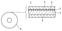
- FIG. 1 is a cross-sectional view showing an anisotropic conductive film to which the present invention is applied.
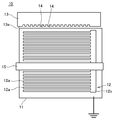
- FIG. 2 is a diagram showing a wiring board and a squeegee for aligning conductive particles.
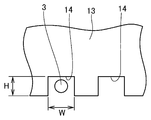
- FIG. 3 is a front view showing a concave portion of the squeegee.
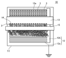
- FIG. 4 is a diagram illustrating a state in which conductive particles are charged and then aligned between wiring patterns with a squeegee.
- FIG. 5 is a diagram showing a state in which conductive particles are charged and then aligned between wiring patterns with a squeegee.
- FIG. 6 is a diagram illustrating a manufacturing process of an anisotropic conductive film.
- FIG. 1 is a cross-sectional view showing an anisotropic conductive film to which the present invention is applied.
- FIG. 2 is a diagram showing a wiring board and a squeegee for aligning conductive particles.
- FIG. 3 is a
- FIG. 7 is a perspective view illustrating a state in which an anisotropic conductive film is attached to a rigid substrate in which a plurality of connection terminals are arranged in parallel.
- FIG. 8 is a diagram for explaining a state in which another anisotropic conductive film is attached to the connection terminal.
- FIG. 9 is a diagram illustrating the inter-particle pitch in a state where the arrangement of the conductive particles is inclined with respect to the longitudinal direction of the anisotropic conductive film (moving direction of the squeegee) and 90 °.
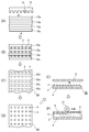
- FIG. 10 is a diagram illustrating a manufacturing process of another anisotropic conductive film.
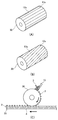
- FIG. 11 is a view showing a roll-shaped substrate
- (A) and (B) are perspective views
- (C) is a cross-sectional view showing a manufacturing process using the roll-shaped substrate.
- 12A and 12B are cross-sectional views showing a manufacturing process of a connection body using a conventional anisotropic conductive film, in which FIG. 12A shows a state before pressure bonding, and FIG. 12B shows a state after pressure bonding.
- the conductive particles are uniformly distributed in a predetermined pattern in the binder resin as an adhesive, and the conductive particles are sandwiched between the connecting terminals facing each other. It is suitably used as an anisotropic conductive film 1 that aims at conduction between the connection terminals.
- a connection body using the conductive adhesive film to which the present invention is applied for example, a connection body in which an IC or a flexible substrate is COG-connected, FOB-connected or FOF-connected using the anisotropic conductive film 1, or the like.
- a connection body in which an IC or a flexible substrate is COG-connected, FOB-connected or FOF-connected using the anisotropic conductive film 1, or the like.
- any device such as a television, a PC, a mobile phone, a game machine, an audio device, a tablet terminal, or an in-vehicle monitor.
- the anisotropic conductive film 1 is a thermosetting adhesive or a photo-curing adhesive such as ultraviolet ray, and is fluidized by being thermally pressed by a crimping tool (not shown) between the connection terminals facing the conductive particles. It is crushed and cured in a state where the conductive particles are crushed by heating or ultraviolet irradiation. Thereby, the anisotropic conductive film 1 electrically and mechanically connects an IC or a flexible substrate to a connection target such as a glass substrate.
- the anisotropic conductive film 1 is conductive to a normal binder resin 2 (adhesive) containing a film-forming resin, a thermosetting resin, a latent curing agent, a silane coupling agent, and the like.
- the particles 3 are arranged in a predetermined pattern, and this thermosetting adhesive composition is supported by a pair of upper and lower first and second base films 4 and 5.
- the first and second base films 4 and 5 are made of, for example, PET (Poly Ethylene Terephthalate), OPP (Oriented Polypropylene), PMP (Poly-4-methylpentene-1), PTFE (Polytetrafluoroethylene), or other release agent such as silicone. Is applied.
- the film forming resin contained in the binder resin 2 is preferably a resin having an average molecular weight of about 10,000 to 80,000.
- the film forming resin include various resins such as an epoxy resin, a modified epoxy resin, a urethane resin, and a phenoxy resin. Among these, phenoxy resin is particularly preferable from the viewpoint of film formation state, connection reliability, and the like.
- thermosetting resin is not particularly limited, and examples thereof include commercially available epoxy resins and acrylic resins.
- the epoxy resin is not particularly limited.
- naphthalene type epoxy resin biphenyl type epoxy resin, phenol novolac type epoxy resin, bisphenol type epoxy resin, stilbene type epoxy resin, triphenolmethane type epoxy resin, phenol aralkyl type epoxy resin.
- an acrylic compound, liquid acrylate, etc. can be selected suitably.
- what made acrylate the methacrylate can also be selected from methyl acrylate, ethyl acrylate, isopropy
- the latent curing agent is not particularly limited, and examples thereof include various curing agents such as a heat curing type and a UV curing type.
- the latent curing agent does not normally react, but is activated by various triggers selected according to applications such as heat, light, and pressure, and starts the reaction.
- the activation method of the thermal activation type latent curing agent includes a method of generating active species (cation, anion, radical) by a dissociation reaction by heating, etc., and it is stably dispersed in the epoxy resin near room temperature, and epoxy at high temperature
- active species cation, anion, radical
- Thermally active latent curing agents include imidazole, hydrazide, boron trifluoride-amine complexes, sulfonium salts, amine imides, polyamine salts, dicyandiamide, etc., and modified products thereof. The above mixture may be sufficient. Among these, a microcapsule type imidazole-based latent curing agent is preferable.
- the silane coupling agent is not particularly limited, and examples thereof include an epoxy type, an amino type, a mercapto sulfide type, and a ureido type. By adding the silane coupling agent, the adhesion at the interface between the organic material and the inorganic material is improved.
- Examples of the conductive particles 3 include any known conductive particles used in the anisotropic conductive film 1.
- Examples of the conductive particles 3 include particles of various metals and metal alloys such as nickel, iron, copper, aluminum, tin, lead, chromium, cobalt, silver, and gold, metal oxide, carbon, graphite, glass, ceramic, Examples thereof include those in which the surface of particles such as plastic is coated with metal, or those in which the surface of these particles is further coated with an insulating thin film.
- examples of the resin particle include an epoxy resin, a phenol resin, an acrylic resin, an acrylonitrile / styrene (AS) resin, a benzoguanamine resin, a divinylbenzene resin, a styrene resin, and the like. Can be mentioned.
- the conductive particles 3 are regularly arranged in a predetermined arrangement pattern, thereby preventing the occurrence of roughness due to aggregation of the conductive particles. Therefore, according to the anisotropic conductive film 1, it is possible to prevent a short circuit between terminals due to agglomeration of conductive particles even when the connection terminals are narrowed. Particles can be captured and the demand for high-density packaging can be met.
- the shape of the anisotropic conductive film 1 is not particularly limited.
- the anisotropic conductive film 1 has a long tape shape that can be wound around a take-up reel 6, and is cut by a predetermined length. can do.
- the adhesive according to the invention is not limited to this, and for example, an insulating adhesive layer made of only the binder resin 2 and a conductive particle-containing layer made of the binder resin 2 containing the conductive particles 3 are laminated. be able to.
- the anisotropic conductive film 1 is manufactured by aligning the conductive particles 3 in a predetermined arrangement pattern on the wiring substrate and then transferring the conductive particles 3 with a film provided with a binder resin layer.
- the wiring substrate 10 on which the conductive particles 3 are arranged has a wiring pattern 12 formed on the insulating substrate 11 according to the arrangement pattern of the conductive particles 3.
- the insulating substrate 11 various known insulating substrates such as a glass epoxy substrate can be used.
- the wiring pattern 12 is formed of, for example, Cu wiring, and can be formed by a known method such as etching or printing.
- the wiring pattern 12 is grounded and is prevented from being charged, thereby preventing magnetic adsorption of the conductive particles 3.
- the wiring pattern 12 is formed in a pattern corresponding to the arrangement pattern of the conductive particles 3 transferred to the binder resin 3 of the anisotropic conductive film 1, and the wiring substrate 10 is electrically conductive particles 3 by a squeegee 13 described later. Is charged and adhered between the wiring patterns 12. Therefore, the shape of the wiring pattern 12 is defined according to the arrangement pattern of the conductive particles 3. For example, as shown in FIG. 2, by arranging a plurality of linear patterns 12 a in parallel, the conductive particles 3 The linear patterns 12a are equally distributed according to the interval between the linear patterns 12a. Each linear pattern 12a is continuous with the ground wiring 12b formed along one side edge of the insulating substrate 11, and is grounded through the ground wiring 12b.
- the squeegee 13 moves on the wiring substrate 10 so that the conductive particles 3 are charged and adhered between the wiring patterns 12 and aligned according to the wiring pattern 12.
- the squeegee 13 has a plurality of recesses 14 formed at predetermined intervals on a sliding side 13 a that slides on the wiring board 10. Each concave portion 14 allows the conductive particles 3 to pass along with the movement of the squeegee 13 and is aligned at a predetermined interval defined by the interval between adjacent concave portions.
- the conductive particles 3 move in the moving direction of the squeegee 13. Are distributed evenly at intervals of the linear patterns 12a and at intervals of the recesses 14 in a direction perpendicular to the moving direction of the squeegee 13.
- each recess 14 is formed with a width W and a height H larger than the average particle diameter of the conductive particles 3, thereby allowing the conductive particles 3 to pass therethrough.
- the recess 14 is preferably formed with a width smaller than twice the average particle diameter of the conductive particles 3. This is because, when the recesses 14 have a width that is twice or more the average particle diameter of the conductive particles 3, the recesses 14 are dispersed even when the conductive particles 3 are allowed to pass therethrough, and the particle capture rate may be reduced.
- the squeegee 13 is prevented from being magnetically attracted to the conductive particles 3 by being prevented from being charged.
- the squeegee 13 is formed of a conductive material such as Ni and is prevented from being charged by being grounded. Further, the squeegee 13 may be prevented from being charged by being formed of a material that is difficult to be charged. Further, such a squeegee 13 can be formed using an electroforming method or other known fine processing techniques.
- the conductive particles 3 are placed on one end of the wiring substrate 10 on which the wiring pattern 12 is formed.
- the static electricity generator 15 is moved from one end side to the other end side of the wiring substrate 10 to charge the conductive particles 3 with charges (for example, negative charges) (FIGS. 4 and 5).
- the squeegee 13 is slid from one end side to the other end side of the wiring board 10.
- the charged conductive particles 3 are charged and adhered between the linear patterns 12 a while passing through the recesses 14 of the squeegee 13.
- the conductive particles 3 are arranged at intervals of the linear pattern 12 a with respect to the moving direction of the squeegee 13 and at intervals of the concave portions 14 with respect to a direction orthogonal to the moving direction of the squeegee 13.
- the conductive particles 3 are placed on the wiring substrate 10 by making the moving direction of the squeegee 13 have an inclination ⁇ of 90 ° with respect to the longitudinal direction of the linear pattern 12a.
- the lattice pattern is uniformly distributed (FIG. 6B).
- the wiring pattern 12 and the squeegee 13 are prevented from being charged by being grounded or the like, the conductive particles 3 charged with electric charges do not adhere to the wiring pattern 12 and the squeegee 13 reliably between the linear patterns 12a. Are distributed.
- the conductive particles 3 distributed on the wiring substrate 10 are transferred to a transfer film.
- the transfer film 20 is formed into a film shape by applying the binder resin 2 described above to one surface of the first base film 4 constituting the anisotropic conductive film 1.
- the transfer film 20 can transfer the conductive particles 3 arranged in a predetermined pattern to the binder resin 2 in the pattern by sticking the surface coated with the binder resin 2 on the wiring substrate 10. .
- the transfer film 20 has the conductive particles 3 arranged at 90 ° with respect to the longitudinal direction by making the longitudinal direction parallel to the moving direction of the squeegee.
- the particles 3 are transferred in a lattice shape and uniformly (FIG. 6D).
- the transfer film 20 to which the conductive particles 3 have been transferred is laminated by the second base film 5 constituting the anisotropic conductive film 1 (FIG. 6E).
- the 2nd base film 5 pushes the electroconductive particle 3 transcribe
- the second base film 5 is bonded to the surface of the transfer film 20 to which the conductive particles 3 are transferred, whereby the conductive particles 3 are bonded to the first and second base films 4 and 5. It is held in the binder resin 2 applied to. Thereby, the anisotropic conductive film 1 in which the binder resin 2 containing the conductive particles 3 is supported by the pair of upper and lower first and second base films 4 and 5 is formed.
- the anisotropic conductive film 1 is pressed into the binder resin 2 applied to the second base film 5 by being appropriately pressed by the laminating roll 21.
- the surface of the anisotropic conductive film 1 on which the conductive particles 3 of the binder resin 2 are pressed is cured, for example, by being irradiated with ultraviolet rays from the first base film 4 side. It is fixed with the transferred pattern.
- the anisotropic conductive film 1 is a connection body in which an IC or a flexible substrate is COG-connected, FOB-connected or FOF-connected, such as a television, a PC, a mobile phone, a game machine, an audio device, a tablet terminal, or an in-vehicle monitor. It can be suitably used for all electronic devices.
- a rigid substrate 22 to which an IC and a flexible substrate are connected via the anisotropic conductive film 1 has a plurality of connection terminals 23 formed in parallel. These connection terminals 23 are miniaturized and narrowed between the connection terminals because of the demand for high-density mounting.
- the anisotropic conductive film 1 is cut in the width direction according to the size of the connection terminal 23, and then the first base film 4 is peeled off, and the parallel direction of the connection terminals 23 is taken as the longitudinal direction. Are pasted on the plurality of connection terminals 23.
- a connection terminal on the IC or flexible substrate side is mounted on the connection terminal 23 via the anisotropic conductive film 1 and is heat-pressed from above with a crimping tool (not shown).
- the anisotropic conductive film 1 is in a state in which the binder resin 2 is softened and the conductive particles 3 are crushed between the opposing connection terminals, and the conductive particles 3 are crushed by heating or ultraviolet irradiation. Harden.
- the anisotropic conductive film 1 electrically and mechanically connects an IC or a flexible substrate to a connection target such as a glass substrate.
- the anisotropic conductive film 1 the conductive particles 3 are transferred in a lattice shape and uniformly over the longitudinal direction. Therefore, the anisotropic conductive film 1 can be surely captured even on the miniaturized connection terminals 23 to improve the electrical conductivity, and the conductive particles 3 are also present between the narrowed connection terminals. A short circuit between adjacent terminals can be prevented without being connected.
- the anisotropic conductive film 30 shown in FIG. 8 is formed so that the arrangement of the conductive particles 3 is inclined with respect to the longitudinal direction.
- the anisotropic conductive film 30 has a narrower pitch P1 of the conductive particles 3 in the longitudinal direction than the anisotropic conductive film 1 because the arrangement of the conductive particles 3 is inclined with respect to the longitudinal direction.
- P1 the pitch of the conductive particles 3 in the longitudinal direction
- anisotropic conductive film 1 because the arrangement of the conductive particles 3 is inclined with respect to the longitudinal direction.
- the anisotropic conductive film 30 has a linear pattern 12a formed on the wiring board 10 inclined by a predetermined angle ⁇ with respect to the moving direction of the squeegee 13.
- the arrays A1 and A2 of the conductive particles 3 aligned between the linear patterns 12a have the inclination ⁇ with respect to the longitudinal direction L of the anisotropic conductive film 30 (moving direction of the squeegee 13).
- FIG. 9B shows the particle arrangements A1 and A2 in the anisotropic conductive film 1 in which the linear pattern 12a is 90 ° with respect to the moving direction of the squeegee.
- the pitch P2 of the conductive particles 3 in the longitudinal direction L corresponds to the interval between the linear patterns 12a. That is, in the anisotropic conductive film 1, the pitch P2 of the conductive particles 3 in the longitudinal direction is defined by the interval P0 between the particle arrays A1 and A2.
- the pitch P1 of the conductive particles 3 in the longitudinal direction L is between the conductive particles 3a and 3b on the particle array A1 and between the conductive particles 3b and the particle array A2. It is defined by the distance between 3c. Therefore, when the interval P0 between the particle arrangements A1 and A2 is the same as that of the anisotropic conductive film 1, the anisotropic conductive film 30 has the pitch P1 of the conductive particles 3 in the longitudinal direction L set to the anisotropic conductive film 1. It can be narrowed compared to.
- a wiring pattern 12 including a plurality of linear patterns 12a is formed on the wiring board 10.
- the linear pattern 12a has an inclination ⁇ of a predetermined angle with respect to the moving direction of the squeegee 13, for example, an angle of 30 ° or more and less than 90 °.
- the conductive particles 3 are evenly distributed and arranged on the wiring substrate 10 at a predetermined interval defined by the angle along the linear pattern 12a and the interval between the recesses 14 (FIG. 10B). .
- the conductive particles 3 dispersedly arranged on the wiring substrate 10 are transferred to the transfer film 20.
- the transfer film 20 can transfer the conductive particles 3 arranged in a predetermined pattern to the binder resin 2 in the pattern by sticking the surface coated with the binder resin 2 on the wiring substrate 10. .
- the transfer film 20 has the longitudinal direction parallel to the moving direction of the squeegee so that the conductive particles 3 correspond to the inclination of the linear pattern 12a with respect to the longitudinal direction. They are arranged at a predetermined angle (FIG. 10D). Then, similarly to the anisotropic conductive film 1, the anisotropic conductive film 30 is obtained by bonding the second base film 5 to the transfer film 20 (FIGS. 10E and 10F).
- the anisotropic conductive film 30 is peeled off from the first base film 4 and pasted on the plurality of connection terminals 23 with the parallel direction of the connection terminals 23 as the longitudinal direction (FIGS. 7 and 8). .
- the connection terminal on the IC or flexible substrate side is mounted on the connection terminal 23 via the anisotropic conductive film 30, and the IC or flexible substrate is heated and pressed by a crimping tool (not shown) from above.
- a connection object such as a glass substrate.
- the anisotropic conductive film 30 can narrow the pitch P of the conductive particles 3 in the longitudinal direction as compared with the anisotropic conductive film 1.
- the anisotropic conductive film 30 is attached with the arrangement direction of the connection terminals 23 as the longitudinal direction, the arrangement pitch of the conductive particles 3 is narrowed with respect to the width direction of the connection terminals 23 in which the arrangement pitch is reduced. Therefore, the particle capture rate on the connection terminal 23 can be improved.
- the anisotropic conductive film 30 preferably has an arrangement angle of the conductive particles 3 with respect to the longitudinal direction of 30 ° or more and less than 90 °. This is because if the angle is less than 30 °, the interval in the arrangement direction of the conductive particles 3 becomes longer, which may cause a decrease in the particle capture rate.
- the wiring board in addition to forming the wiring board in a plate shape, it may be formed in a roll shape as shown in FIG.
- the roll-shaped substrate 30 rolls on the surface of the transfer film 20 on which the binder resin 2 is applied while the wiring pattern 12 is formed on the surface. Then, as shown in FIG. 11C, the roll-shaped substrate 30 is supplied with the conductive particles 3 on the upstream side in the rolling direction and charged with electric charge, and then the squeegee 13 is slid, Prior to contact with the transfer film 20, the conductive particles 3 are aligned and charged in a predetermined pattern corresponding to the wiring pattern 12.
- the linear pattern 12 a of the wiring pattern 12 formed on the roll surface has an angle of 90 ° with respect to the rolling direction of the roll, so that the conductive pattern is electrically conductive with respect to the longitudinal direction.
- the anisotropic conductive film 1 to which the conductive particles 3 are transferred in a lattice shape can be formed (FIG. 11A).
- the roll-shaped substrate 30 has a predetermined inclination (for example, 30 ° or more and less than 90 °) with respect to the rolling direction of the roll, so that the linear substrate 12a is compared with the anisotropic conductive film 1.
- the anisotropic conductive film 30 with which the pitch P of the electroconductive particle 3 in a longitudinal direction was narrowed can be formed (FIG.11 (B)).
- the electrically conductive particles 3 charged by sliding the squeegee 13 from one end side to the other end side of the wiring board 10 pass through the recess 14 of the squeegee 13. However, charging adheres between the linear patterns 12a. At this time, the conductive particles 3 are uniformly distributed at intervals of the linear patterns 12a with respect to the moving direction of the squeegee 13 and at intervals of the concave portions 14 with respect to a direction perpendicular to the moving direction of the squeegee 13. Is done.
- the aggregate in which a plurality of conductive particles 3 are connected is within 20%, preferably within 10%, more preferably 5% of the total number of conductive particles.
- the size of the aggregate is preferably at most 8 times the average particle diameter of the conductive particles, more preferably 5 times or less.
- the size of the aggregate here includes the maximum length of the aggregate to which the conductive particles 3 are connected.
- the anisotropic conductive films according to Examples and Comparative Examples are used as binder resins.
- Phenoxy resin (YP-50, manufactured by Nippon Steel & Sumikin Chemical Co., Ltd.) 60 parts by mass epoxy resin (jER828 manufactured by Mitsubishi Chemical Co., Ltd.) 40 parts by mass Cationic curing agent (SI-60L, manufactured by Sanshin Chemical Industry Co., Ltd.) 2 parts by mass
- the compounded resin composition was used.
- the anisotropic conductive films according to Examples and Comparative Examples were prepared by preparing a mixed solution in which these resin compositions were adjusted so as to have a solid content of 50% with toluene, and after coating on a PET film having a thickness of 50 ⁇ m, It dried for 5 minutes in 80 degreeC oven. This obtained the anisotropic conductive film which has the binder resin 2 of thickness 20 micrometers.
- AUL704 (average particle size: 4 ⁇ m, manufactured by Sekisui Chemical Co., Ltd.) was used as the conductive particles in the anisotropic conductive films according to Examples and Comparative Examples.
- a glass substrate (trade name: 1737F, manufactured by Corning, size: 50 mm ⁇ 30 mm, thickness: 0.5 mm) on which an aluminum wiring pattern corresponding to the pattern of the IC chip was formed was used.
- An anisotropic conductive film according to Examples and Comparative Examples is disposed on this glass substrate, and an IC chip (size: 1.5 mm ⁇ 13.0 mm, thickness: 0.5 mm, gold) is disposed on the anisotropic conductive film.
- Bump size: 25 ⁇ m ⁇ 140 ⁇ m, bump height: 15 ⁇ m, pitch: 7.5 ⁇ m) were placed and heated and pressed to connect the IC chip and the aluminum wiring pattern glass substrate.
- the pressure bonding conditions were 180 ° C., 80 MPa, and 5 seconds.
- Example 1 the conductive particles were manufactured by aligning the conductive particles in a predetermined arrangement pattern on the wiring substrate, and then transferring the conductive particles using a film provided with a binder resin layer.
- a plurality of linear patterns are formed in parallel by Cu wiring, and each linear pattern is grounded to prevent charging.
- the concave part having a width of 6 ⁇ m and a height of 6 ⁇ m is formed at regular intervals on the squeegee that moves on the wiring board. Further, the squeegee is formed of Ni and grounded to prevent charging.
- the static electricity generator is moved from one end side to the other end side of the wiring board to charge the conductive particles with negative charges.
- the squeegee is slid from one end side to the other end side of the wiring board.
- the movement direction of the squeegee is set to 90 ° with respect to the longitudinal direction of the linear pattern.
- the conductive particles are distributed on the wiring board in a lattice-like and uniform manner at predetermined intervals defined by the linear pattern and the recesses (see FIG. 6B).
- the conductive particles dispersed and arranged on the wiring board are transferred to a PET film coated with the above-described binder resin.
- the conductive particles are transferred in a lattice shape and uniformly over the longitudinal direction (see FIGS. 6C and 6D).
- This anisotropic conductive film was affixed on a plurality of connection terminals with the parallel direction of the connection terminals of the aluminum wiring pattern formed on the glass substrate as the longitudinal direction (see FIG. 7).
- Example 2 In Example 2, an anisotropic conductive film was obtained under the same conditions as in Example 1 except that the width of the concave portion of the squeegee was 5 ⁇ m.
- Example 3 In Example 3, an anisotropic conductive film was obtained under the same conditions as in Example 1 except that the width of the concave portion of the squeegee was set to 7 ⁇ m.
- Example 4 In Example 4, an anisotropic conductive film was obtained under the same conditions as in Example 1 except that the width of the concave portion of the squeegee was 9 ⁇ m.
- Example 5 the moving direction of the squeegee has an inclination of 30 ° with respect to the longitudinal direction of the linear pattern.
- the conductive particles are dispersed and arranged on the wiring board at an angle along the linear pattern and at a predetermined interval defined by the recesses (see FIG. 10B).
- the squeegee recess dimensions are the same as in the first embodiment.
- the conductive particles dispersed and arranged on the wiring board are transferred to the PET film.
- the conductive particles are arranged at a predetermined angle corresponding to the inclination of the linear pattern with respect to the longitudinal direction (FIG. 10 (C ) (D)).
- an anisotropic conductive film was obtained by laminating the second PET film to the PET film.
- Example 6 In Example 6, an anisotropic conductive film was obtained under the same conditions as Example 5 except that the moving direction of the squeegee had an inclination of 60 ° with respect to the longitudinal direction of the linear pattern.
- Example 7 In Example 7, an anisotropic conductive film was obtained under the same conditions as Example 5 except that the moving direction of the squeegee had an inclination of 15 ° with respect to the longitudinal direction of the linear pattern.
- Comparative Example 1 an anisotropic conductive film was obtained by a conventional manufacturing method. That is, the anisotropic conductive film shape
- This anisotropic conductive film was affixed on a plurality of connection terminals with the parallel direction of the connection terminals of the aluminum wiring pattern formed on the glass substrate as the longitudinal direction.
- Comparative Example 2 In Comparative Example 2, an adhesive layer was formed by applying an acrylic polymer on a 100 ⁇ m unstretched copolymer polypropylene film and drying. A single particle conductive particle layer having a filling rate of 60% was formed by filling conductive particles on one side of the pressure-sensitive adhesive layer and eliminating conductive particles that did not reach the pressure sensitive adhesive by air blowing.
- the polypropylene film on which the conductive particles are fixed is stretched up to 2.0 times at a rate of 10% / second in both longitudinal and lateral directions at 135 ° C. using a test biaxial stretching apparatus, and gradually reaches room temperature. Cooled to obtain an array sheet.
- Example 1 After overlaying a PET film (transfer film) coated with a binder resin on the conductive particle side of the array sheet and laminating under conditions of 60 ° C. and 0.3 MPa, the conductive particles are embedded in the binder resin. The polypropylene film and the adhesive were peeled off. Thereafter, as in Example 1, an anisotropic conductive film was obtained by laminating the second PET film to the PET film.
- This anisotropic conductive film was affixed on a plurality of connection terminals with the parallel direction of the connection terminals of the aluminum wiring pattern formed on the glass substrate as the longitudinal direction.
- connection body sample which connected IC on the glass substrate using the anisotropic conductive film which concerns on each of these Examples and a comparative example was manufactured. And about each connection body sample, the conduction
- the conduction resistance between the IC chip and the connection terminal formed on the glass substrate is as low as 0.8 ⁇ or less, and the short ratio between the terminals is also 1 ppm or less. Met.
- Comparative Example 1 although the conduction resistance was as low as 0.2 ⁇ , the short ratio between the terminals was as high as 3000 ppm. Similarly, in Comparative Example 2, although the conduction resistance was as low as 0.2 ⁇ , the short ratio between the terminals was as high as 3000 ppm.
- connection terminals are miniaturized, and the connection terminals This is because a high particle trapping rate can be maintained even for the narrowing of the gap, and the agglomeration of particles can be prevented to prevent a short circuit between the narrowed terminals.
- Comparative Example 1 since the conductive particles are randomly dispersed in the binder resin, there are places where the conductive particles are concentrated and dispersed in the binder resin, and between the narrowed adjacent terminals. Conductive particles were connected, and short-circuiting between terminals occurred frequently at 3000 ppm.
- Examples 1 to 3 in which the recess width of the squeegee is less than 2 times are conducted more than 2 times while the conduction resistance is 0.2 to 0.3 ( ⁇ ).
- the conduction resistance increased to 2.0 ( ⁇ ). This is due to the fact that the particles are dispersed and arranged by widening the recess width of the squeegee through which the conductive particles pass, and the particle capture rate is slightly reduced. From this, it can be seen that the recess width of the squeegee is preferably less than twice the average particle diameter of the conductive particles.
- Example 5 to 7 in which the moving direction of the squeegee has a predetermined inclination with respect to the linear pattern, in Examples 5 and 6 where the inclination is 30 ° and 60 °, the conduction resistance is 0. 1 ( ⁇ ), which is lower than those in Examples 1 to 4 in which the moving direction of the squeegee is 90 ° with respect to the linear pattern.
- the arrangement of the conductive particles has a predetermined inclination with respect to the longitudinal direction of the anisotropic conductive film. Therefore, when the anisotropic conductive film is attached along the parallel direction of the connection terminals, This is because the particle pitch in the width direction is narrowed and many particles are trapped even in the miniaturized connection terminal.
- Example 7 by setting the inclination to 15 °, the particle pitch on the particle arrangement of the anisotropic conductive film was increased, so that the particle trapping rate in the longitudinal direction of the connection terminal was reduced to 0.8 ( ⁇ ) and the conduction resistance increased slightly. From this, it is understood that the moving direction of the squeegee is preferably 30 ° or more with respect to the linear pattern.
Landscapes
- Chemical & Material Sciences (AREA)
- Engineering & Computer Science (AREA)
- Organic Chemistry (AREA)
- Manufacturing & Machinery (AREA)
- Microelectronics & Electronic Packaging (AREA)
- Inorganic Chemistry (AREA)
- Non-Insulated Conductors (AREA)
- Electric Connection Of Electric Components To Printed Circuits (AREA)
- Manufacturing Of Electrical Connectors (AREA)
- Wire Bonding (AREA)
- Adhesive Tapes (AREA)
- Manufacturing Of Printed Wiring (AREA)
Abstract
Description
本出願は、日本国において2013年7月29日に出願された日本特許出願番号特願2013-157098を基礎として優先権を主張するものであり、これらの出願は参照されることにより、本出願に援用される。
本発明が適用された導電性接着フィルムは、接着剤となるバインダー樹脂中に導電性粒子が所定のパターンで均等に分散配置され、相対向する接続端子間に導電性粒子が挟持されることにより当該接続端子間の導通を図る異方性導電フィルム1として好適に用いられる。また、本発明が適用された導電性接着フィルムを用いた接続体としては、例えば、異方性導電フィルム1を用いてICやフレキシブル基板がCOG接続、FOB接続あるいはFOF接続された接続体、その他の接続体であって、テレビやPC、携帯電話、ゲーム機、オーディオ機器、タブレット端末あるいは車載用モニタ等のあらゆる機器に好適に用いることができる。
導電性粒子3としては、異方性導電フィルム1において使用されている公知の何れの導電性粒子を挙げることができる。導電性粒子3としては、例えば、ニッケル、鉄、銅、アルミニウム、錫、鉛、クロム、コバルト、銀、金等の各種金属や金属合金の粒子、金属酸化物、カーボン、グラファイト、ガラス、セラミック、プラスチック等の粒子の表面に金属をコートしたもの、或いは、これらの粒子の表面に更に絶縁薄膜をコートしたもの等が挙げられる。樹脂粒子の表面に金属をコートしたものである場合、樹脂粒子としては、例えば、エポキシ樹脂、フェノール樹脂、アクリル樹脂、アクリロニトリル・スチレン(AS)樹脂、ベンゾグアナミン樹脂、ジビニルベンゼン系樹脂、スチレン系樹脂等の粒子を挙げることができる。
次いで、異方性導電フィルム1の製造方法について説明する。異方性導電フィルム1は、導電性粒子3を配線基板上に所定の配列パターンに整列させた後、バインダー樹脂層が設けられたフィルムによって導電性粒子3を転写することにより製造される。
異方性導電フィルム1は、ICやフレキシブル基板がCOG接続、FOB接続あるいはFOF接続された接続体等であって、テレビやPC、携帯電話、ゲーム機、オーディオ機器、タブレット端末あるいは車載用モニタ等のあらゆる電子機器に好適に用いることができる。
次いで、本発明が適用された異方性導電フィルムの第2の形態について説明する。なお、以下では上述した異方性導電フィルム1や配線基板10と同一の構成については同一の符号を付してその詳細を省略する。
次いで、異方性導電フィルム30の製造工程について説明する。図10(A)に示すように、配線基板10に複数の直線状パターン12aからなる配線パターン12を形成する。このとき、直線状パターン12aは、スキージ13の移動方向に対して所定の角度、例えば30°以上90°未満の角度の傾きθを有する。
なお、異方性導電フィルム30は、長手方向に対する導電性粒子3の配列角度が30°以上90°未満とすることが好ましい。30°未満とすると、導電性粒子3の配列方向における間隔が長くなり、かえって粒子捕捉率の低下を招くおそれが生じるからである。
また、配線基板は、板状に形成する他にも、図11に示すように、ロール状に形成してもよい。ロール状基板30は、表面に配線パターン12が形成されるとともに、転写フィルム20のバインダー樹脂2が塗布された面上を転動する。そして、図11(C)に示すように、ロール状基板30には、転動方向上流側において導電性粒子3が供給されるとともに電荷が帯電され、その後スキージ13が摺動されることにより、転写フィルム20と接触する前に導電性粒子3が配線パターン12に応じた所定のパターンに整列、帯電付着される。
なお、上述したように、本発明によれば、スキージ13を配線基板10の一端側から他端側へ摺動させることにより電荷を帯びた導電性粒子3が、スキージ13の凹部14を通過しながら直線状パターン12a間に帯電付着する。このとき、導電性粒子3は、スキージ13の移動方向に対しては直線状パターン12aの間隔で、またスキージ13の移動方向と直行する方向に対しては凹部14の間隔で、均等に分散配置される。
また、導電性粒子3は、スキージ13の凹部14を通過しながら直線状パターン12a間に帯電付着することから、スキージ13との摺接痕が発生する。例えば、導電性粒子3としてめっき粒子を用いた場合には、表面の一部が剥離し、あるいはめくれている。また導電性粒子3として金属粒子を用いた場合には、導電性粒子3の一部に変形が生じる場合もある。このような摺接痕は、導電性粒子3の表面積の5%以上に生じることにより、バインダー樹脂2の転写時や異方性導電フィルム1の熱加圧時等において導電性粒子3の流動が抑制される。また、摺接痕が発生した導電性粒子3が全体の30%以内であれば、導通性能に影響はないが、全導電性粒子数の15%以内とすることが好ましい。
フェノキシ樹脂(YP‐50、新日鉄住金化学株式会社製) 60質量部
エポキシ樹脂(jER828 三菱化学株式会社製) 40質量部
カチオン系硬化剤(SI‐60L 三新化学工業株式会社製) 2質量部
を配合した樹脂組成物を用いた。
実施例1では、導電性粒子を配線基板上に所定の配列パターンに整列させた後、バインダー樹脂層が設けられたフィルムによって導電性粒子を転写することにより製造した。実施例1に係る配線基板には、Cu配線によって複数の直線状パターンが平行に形成されるとともに、各直線状パターンはアースされ、帯電が防止されている。
実施例2では、スキージの凹部の幅を5μmとした他は、実施例1と同じ条件で異方性導電フィルムを得た。
実施例3では、スキージの凹部の幅を7μmとした他は、実施例1と同じ条件で異方性導電フィルムを得た。
実施例4では、スキージの凹部の幅を9μmとした他は、実施例1と同じ条件で異方性導電フィルムを得た。
実施例5では、スキージの移動方向を、直線状パターンの長手方向に対して30°の傾きを有するようにした。これにより、導電性粒子は、配線基板上に直線状パターンに沿った角度、及び凹部によって規定される所定の間隔で、分散配置される(図10(B)参照)。なお、スキージの凹部寸法は実施例1と同じである。
実施例6では、スキージの移動方向を、直線状パターンの長手方向に対して60°の傾きを有するようにした他は、実施例5と同じ条件で異方性導電フィルムを得た。
実施例7では、スキージの移動方向を、直線状パターンの長手方向に対して15°の傾きを有するようにした他は、実施例5と同じ条件で異方性導電フィルムを得た。
比較例1では、従来通りの製法で異方性導電フィルムを得た。すなわち、上述したバインダー樹脂中に導電性粒子を分散した樹脂組成物をPETフィルム上に塗布、乾燥することによりフィルム状に成形した異方性導電フィルムを得た。比較例1に係る異方性導電フィルムは、バインダー樹脂中に導電性粒子がランダムに配置されている。
比較例2では、100μm無延伸共重合ポリプロピレンフィルム上にアクリルポリマーを塗布、乾燥することにより粘着剤層を形成した。この粘着材層上に導電性粒子を一面に充填し、エアーブローにより粘着剤に到達していない導電性粒子を排除することにより、充填率60%の単層導電性粒子層を形成した。

Claims (13)
- 導電性粒子の配列パターンに応じて形成され帯電が防止された配線を有する配線基板上に、導電性粒子を散布し、上記導電性粒子を帯電させる工程と、
上記配線基板上にスキージを移動させることによって、上記帯電された導電性粒子を、上記配線パターンに応じた所定の配列パターンに整列させる工程と、
上記配線基板と接着剤層が形成された転写フィルムとを貼り合わせ、所定の配列パターンに整列された上記導電性粒子を上記接着剤層に転写する工程とを有する導電性接着フィルムの製造方法。 - 上記スキージは、上記導電性粒子の配列パターンに応じて、上記導電性粒子を通過させる凹部が形成されている請求項1記載の導電性接着フィルムの製造方法。
- 上記配線は、複数の直線状パターンが平行に配列され、
上記スキージの移動方向は、上記直線状パターンの長手方向に対して90°の傾きを有する請求項2記載の導電性接着フィルムの製造方法。 - 上記配線は、複数の直線状パターンが平行に配列され、
上記スキージの移動方向は、上記直線状パターンの長手方向に対して30°以上90°未満の傾きを有し、
上記転写フィルムは、長手方向を上記スキージの移動方向と同方向にして上記配線基板上に貼り合わされる請求項2記載の導電性接着フィルムの製造方法。 - 上記スキージは、帯電が防止されている請求項1~4のいずれか1項に記載の導電性接着フィルムの製造方法。
- 上記スキージは、上記凹部の幅が上記導電性粒子の平均粒子径よりも大きく、かつ上記導電性粒子の平均粒子径の2倍より小さい請求項2~4のいずれか1項に記載の導電性接着フィルムの製造方法。
- 上記配線基板は、ロール状に形成され、
上記配線基板が回転することにより、上記導電性粒子の散布及び帯電、上記スキージによる整列、上記転写フィルムへの転写の一連の工程を繰り返し連続して行う請求項1~4のいずれか1項に記載の導電性接着フィルムの製造方法。 - 上記スキージは、エレクトロフォーミング法によって形成される請求項2~4のいずれか1項に記載の導電性接着フィルムの製造方法。
- ベースフィルムと、
上記ベースフィルム上に積層されたバインダー樹脂と、
上記バインダー樹脂に、所定の配列パターンで、規則的に分散配置された導電性粒子とを備え、
複数の上記導電性粒子の凝集体が、粒子数全体の20%以内である導電性接着フィルム。 - ベースフィルムと、
上記ベースフィルム上に積層されたバインダー樹脂と、
上記バインダー樹脂に、所定の配列パターンで、規則的に分散配置された導電性粒子とを備え、
複数の上記導電性粒子のうち、表面に摺接痕が表面積の5%以上に発生しているものが粒子数全体の30%以内である導電性接着フィルム。 - 上記1~8のいずれか1項に記載の製造方法によって製造された請求項9又は請求項10に記載の導電性接着フィルム。
- 導電性粒子が配列された異方性導電フィルムによって複数並列された端子同士が接続された接続体の製造方法において、
上記異方性導電フィルムは、
導電性粒子の配列パターンに応じて形成され帯電が防止された配線を有する配線基板上に、導電性粒子を散布し、上記導電性粒子を帯電させる工程と、
上記配線基板上にスキージを移動させることによって、上記帯電された導電性粒子を、上記配線パターンに応じた所定の配列パターンに整列させる工程と、
上記配線基板と接着剤層が形成された転写フィルムとを貼り合わせ、所定の配列パターンに整列された上記導電性粒子を上記接着剤層に転写する工程とにより製造され、
上記端子間に、該端子の並列方向を長手方向として挟持される接続体の製造方法。 - 上記異方性導電フィルムは、長手方向が、上記導電性粒子の配列方向に対して30°以上90°未満の傾きを有する請求項12記載の接続体の製造方法。
Priority Applications (5)
| Application Number | Priority Date | Filing Date | Title |
|---|---|---|---|
| CN201480039800.2A CN105359354B (zh) | 2013-07-29 | 2014-07-28 | 导电性粘接膜的制造方法、导电性粘接膜、连接体的制造方法 |
| KR1020167000743A KR101843297B1 (ko) | 2013-07-29 | 2014-07-28 | 도전성 접착 필름의 제조 방법, 도전성 접착 필름, 접속체의 제조 방법 |
| HK16107919.5A HK1220044B (en) | 2013-07-29 | 2014-07-28 | Method for manufacturing electroconductive adhesive film, electroconductive adhesive film, and method for manufacturing connection body |
| US14/904,456 US9816012B2 (en) | 2013-07-29 | 2014-07-28 | Method for manufacturing electrically conductive adhesive film, electrically conductive adhesive film, and method for manufacturing connector |
| US15/729,162 US10501661B2 (en) | 2013-07-29 | 2017-10-10 | Method for manufacturing electrically conductive adhesive film, electrically conductive adhesive film, and method for manufacturing connector |
Applications Claiming Priority (2)
| Application Number | Priority Date | Filing Date | Title |
|---|---|---|---|
| JP2013157098A JP6151597B2 (ja) | 2013-07-29 | 2013-07-29 | 導電性接着フィルムの製造方法、導電性接着フィルム、接続体の製造方法 |
| JP2013-157098 | 2013-07-29 |
Related Child Applications (2)
| Application Number | Title | Priority Date | Filing Date |
|---|---|---|---|
| US14/904,456 A-371-Of-International US9816012B2 (en) | 2013-07-29 | 2014-07-28 | Method for manufacturing electrically conductive adhesive film, electrically conductive adhesive film, and method for manufacturing connector |
| US15/729,162 Division US10501661B2 (en) | 2013-07-29 | 2017-10-10 | Method for manufacturing electrically conductive adhesive film, electrically conductive adhesive film, and method for manufacturing connector |
Publications (1)
| Publication Number | Publication Date |
|---|---|
| WO2015016167A1 true WO2015016167A1 (ja) | 2015-02-05 |
Family
ID=52431700
Family Applications (1)
| Application Number | Title | Priority Date | Filing Date |
|---|---|---|---|
| PCT/JP2014/069793 Ceased WO2015016167A1 (ja) | 2013-07-29 | 2014-07-28 | 導電性接着フィルムの製造方法、導電性接着フィルム、接続体の製造方法 |
Country Status (6)
| Country | Link |
|---|---|
| US (2) | US9816012B2 (ja) |
| JP (1) | JP6151597B2 (ja) |
| KR (1) | KR101843297B1 (ja) |
| CN (2) | CN105359354B (ja) |
| HK (1) | HK1259334A1 (ja) |
| WO (1) | WO2015016167A1 (ja) |
Families Citing this family (16)
| Publication number | Priority date | Publication date | Assignee | Title |
|---|---|---|---|---|
| JP6151597B2 (ja) * | 2013-07-29 | 2017-06-21 | デクセリアルズ株式会社 | 導電性接着フィルムの製造方法、導電性接着フィルム、接続体の製造方法 |
| JP2015079586A (ja) * | 2013-10-15 | 2015-04-23 | デクセリアルズ株式会社 | 異方性導電フィルム |
| JP6746942B2 (ja) * | 2016-02-20 | 2020-08-26 | デクセリアルズ株式会社 | 異方導電性フィルム及び接続構造体 |
| CN114582545B (zh) * | 2015-03-20 | 2024-10-29 | 迪睿合株式会社 | 各向异性导电性膜及连接构造体 |
| WO2017061539A1 (ja) * | 2015-10-07 | 2017-04-13 | デクセリアルズ株式会社 | 異方性導電フィルム及び接続構造体 |
| WO2017191772A1 (ja) * | 2016-05-05 | 2017-11-09 | デクセリアルズ株式会社 | フィラー配置フィルム |
| JP7095227B2 (ja) * | 2016-05-05 | 2022-07-05 | デクセリアルズ株式会社 | 異方性導電フィルム |
| US12550783B2 (en) | 2016-05-17 | 2026-02-10 | Taiwan Semiconductor Manufacturing Company, Ltd. | Device and method for UBM/RDL routing |
| JP6329669B2 (ja) * | 2017-05-25 | 2018-05-23 | デクセリアルズ株式会社 | 導電性接着フィルムの製造方法、導電性接着フィルム、接続体の製造方法 |
| JP7160302B2 (ja) * | 2018-01-31 | 2022-10-25 | 三国電子有限会社 | 接続構造体および接続構造体の作製方法 |
| JP7185252B2 (ja) | 2018-01-31 | 2022-12-07 | 三国電子有限会社 | 接続構造体の作製方法 |
| JP7046351B2 (ja) | 2018-01-31 | 2022-04-04 | 三国電子有限会社 | 接続構造体の作製方法 |
| KR102519126B1 (ko) * | 2018-03-30 | 2023-04-06 | 삼성디스플레이 주식회사 | 표시 장치 |
| KR102942110B1 (ko) * | 2019-11-18 | 2026-03-24 | 삼성디스플레이 주식회사 | 표시 장치의 제조 방법 |
| CN115209635B (zh) * | 2022-07-06 | 2025-10-24 | 北京梦之墨科技有限公司 | 一种导电结构及其制作方法 |
| CN117377229B (zh) * | 2023-12-07 | 2024-02-20 | 深圳清大电子科技有限公司 | 一种用于导电膜贴合的热压工艺与设备 |
Citations (3)
| Publication number | Priority date | Publication date | Assignee | Title |
|---|---|---|---|---|
| JPH11260164A (ja) * | 1998-03-05 | 1999-09-24 | Jsr Corp | 異方導電性シートの製造方法及びその製造装置 |
| JP2010033793A (ja) * | 2008-07-28 | 2010-02-12 | Tokai Rubber Ind Ltd | 粒子転写膜の製造方法 |
| JP2010251337A (ja) * | 2010-08-05 | 2010-11-04 | Sony Chemical & Information Device Corp | 異方性導電膜及びその製造方法並びに接続構造体 |
Family Cites Families (11)
| Publication number | Priority date | Publication date | Assignee | Title |
|---|---|---|---|---|
| JP3472987B2 (ja) * | 1993-01-29 | 2003-12-02 | 日立化成工業株式会社 | 接続部材の製造法及びその製造装置 |
| US5616206A (en) * | 1993-06-15 | 1997-04-01 | Ricoh Company, Ltd. | Method for arranging conductive particles on electrodes of substrate |
| US6528346B2 (en) * | 1994-01-20 | 2003-03-04 | Fujitsu Limited | Bump-forming method using two plates and electronic device |
| US6063701A (en) * | 1996-09-14 | 2000-05-16 | Ricoh Company, Ltd. | Conductive particle transferring method |
| JP2002075580A (ja) * | 2000-09-04 | 2002-03-15 | Sekisui Chem Co Ltd | 異方導電フィルムの製造方法 |
| TWI332027B (en) * | 2000-12-28 | 2010-10-21 | Hitachi Chemical Co Ltd | Circuit connecting adhesive with anisotropic conductivity connecting method of circuit board and circuit connecting construction by using the adhesive |
| JP3995942B2 (ja) * | 2002-01-29 | 2007-10-24 | 旭化成株式会社 | 異方性を有する導電性接着シートの製造方法 |
| WO2005054388A1 (ja) * | 2003-12-04 | 2005-06-16 | Asahi Kasei Emd Corporation | 異方導電性接着シート及び接続構造体 |
| US20060280912A1 (en) * | 2005-06-13 | 2006-12-14 | Rong-Chang Liang | Non-random array anisotropic conductive film (ACF) and manufacturing processes |
| JP4789738B2 (ja) | 2006-07-28 | 2011-10-12 | 旭化成イーマテリアルズ株式会社 | 異方導電性フィルム |
| JP6151597B2 (ja) * | 2013-07-29 | 2017-06-21 | デクセリアルズ株式会社 | 導電性接着フィルムの製造方法、導電性接着フィルム、接続体の製造方法 |
-
2013
- 2013-07-29 JP JP2013157098A patent/JP6151597B2/ja active Active
-
2014
- 2014-07-28 WO PCT/JP2014/069793 patent/WO2015016167A1/ja not_active Ceased
- 2014-07-28 KR KR1020167000743A patent/KR101843297B1/ko active Active
- 2014-07-28 CN CN201480039800.2A patent/CN105359354B/zh active Active
- 2014-07-28 US US14/904,456 patent/US9816012B2/en active Active
- 2014-07-28 CN CN201810155342.9A patent/CN108384475A/zh active Pending
-
2017
- 2017-10-10 US US15/729,162 patent/US10501661B2/en active Active
-
2019
- 2019-01-31 HK HK19101700.8A patent/HK1259334A1/zh unknown
Patent Citations (3)
| Publication number | Priority date | Publication date | Assignee | Title |
|---|---|---|---|---|
| JPH11260164A (ja) * | 1998-03-05 | 1999-09-24 | Jsr Corp | 異方導電性シートの製造方法及びその製造装置 |
| JP2010033793A (ja) * | 2008-07-28 | 2010-02-12 | Tokai Rubber Ind Ltd | 粒子転写膜の製造方法 |
| JP2010251337A (ja) * | 2010-08-05 | 2010-11-04 | Sony Chemical & Information Device Corp | 異方性導電膜及びその製造方法並びに接続構造体 |
Also Published As
| Publication number | Publication date |
|---|---|
| CN105359354B (zh) | 2019-01-08 |
| US10501661B2 (en) | 2019-12-10 |
| JP6151597B2 (ja) | 2017-06-21 |
| KR101843297B1 (ko) | 2018-03-28 |
| US9816012B2 (en) | 2017-11-14 |
| HK1259334A1 (zh) | 2019-11-29 |
| HK1220044A1 (zh) | 2017-04-21 |
| KR20160037160A (ko) | 2016-04-05 |
| US20180044558A1 (en) | 2018-02-15 |
| JP2015026584A (ja) | 2015-02-05 |
| US20160168428A1 (en) | 2016-06-16 |
| CN105359354A (zh) | 2016-02-24 |
| CN108384475A (zh) | 2018-08-10 |
Similar Documents
| Publication | Publication Date | Title |
|---|---|---|
| JP6151597B2 (ja) | 導電性接着フィルムの製造方法、導電性接着フィルム、接続体の製造方法 | |
| US11139629B2 (en) | Method for manufacturing electrically conductive adhesive film, electrically conductive adhesive film, and method for manufacturing connector | |
| JP6289831B2 (ja) | 導電性接着フィルムの製造方法、導電性接着フィルム、接続体の製造方法 | |
| CN106415937B (zh) | 连接体及连接体的制造方法 | |
| JP2013207115A (ja) | 接続構造体及びその製造方法、電子部品及びその製造方法、電子部品の接続方法 | |
| JP2015135878A (ja) | 接続体、接続体の製造方法、接続方法、異方性導電接着剤 | |
| JP2014192337A (ja) | 接続体の製造方法、電子部品の接続方法、接続構造体 | |
| JP6329669B2 (ja) | 導電性接着フィルムの製造方法、導電性接着フィルム、接続体の製造方法 | |
| JP6370562B2 (ja) | 接続体の製造方法、フレキシブル基板の接続方法、接続体及びフレキシブル基板 | |
| JP2018078118A (ja) | 導電性接着フィルム、接続体の製造方法 | |
| WO2016114381A1 (ja) | 接続構造体 | |
| HK40008376A (en) | Method for producing conductive adhesive film, conductive adhesive film, and method for producing connection body | |
| HK40008376B (en) | Method for producing conductive adhesive film, conductive adhesive film, and method for producing connection body | |
| HK1220044B (en) | Method for manufacturing electroconductive adhesive film, electroconductive adhesive film, and method for manufacturing connection body | |
| JP2014107305A (ja) | 接続構造体の製造方法、接続構造体及び接続方法 | |
| JP2019140413A (ja) | 接続体、接続体の製造方法、接続方法 | |
| HK40031434A (en) | Connection body, connection body production method, connection method, anisotropic conductive adhesive | |
| HK1229956A1 (en) | Connection body and connection body production method |
Legal Events
| Date | Code | Title | Description |
|---|---|---|---|
| WWE | Wipo information: entry into national phase |
Ref document number: 201480039800.2 Country of ref document: CN |
|
| 121 | Ep: the epo has been informed by wipo that ep was designated in this application |
Ref document number: 14831638 Country of ref document: EP Kind code of ref document: A1 |
|
| ENP | Entry into the national phase |
Ref document number: 20167000743 Country of ref document: KR Kind code of ref document: A |
|
| WWE | Wipo information: entry into national phase |
Ref document number: 14904456 Country of ref document: US |
|
| NENP | Non-entry into the national phase |
Ref country code: DE |
|
| 122 | Ep: pct application non-entry in european phase |
Ref document number: 14831638 Country of ref document: EP Kind code of ref document: A1 |