WO2015016040A1 - 走査電子顕微鏡 - Google Patents
走査電子顕微鏡 Download PDFInfo
- Publication number
- WO2015016040A1 WO2015016040A1 PCT/JP2014/068529 JP2014068529W WO2015016040A1 WO 2015016040 A1 WO2015016040 A1 WO 2015016040A1 JP 2014068529 W JP2014068529 W JP 2014068529W WO 2015016040 A1 WO2015016040 A1 WO 2015016040A1
- Authority
- WO
- WIPO (PCT)
- Prior art keywords
- detector
- electron microscope
- scanning electron
- sample
- electrons
- Prior art date
- Legal status (The legal status is an assumption and is not a legal conclusion. Google has not performed a legal analysis and makes no representation as to the accuracy of the status listed.)
- Ceased
Links
Images






Classifications
-
- H—ELECTRICITY
- H01—ELECTRIC ELEMENTS
- H01J—ELECTRIC DISCHARGE TUBES OR DISCHARGE LAMPS
- H01J37/00—Discharge tubes with provision for introducing objects or material to be exposed to the discharge, e.g. for the purpose of examination or processing thereof
- H01J37/26—Electron or ion microscopes; Electron or ion diffraction tubes
- H01J37/261—Details
- H01J37/265—Controlling the tube; circuit arrangements adapted to a particular application not otherwise provided, e.g. bright-field-dark-field illumination
-
- H—ELECTRICITY
- H01—ELECTRIC ELEMENTS
- H01J—ELECTRIC DISCHARGE TUBES OR DISCHARGE LAMPS
- H01J37/00—Discharge tubes with provision for introducing objects or material to be exposed to the discharge, e.g. for the purpose of examination or processing thereof
- H01J37/02—Details
- H01J37/244—Detectors; Associated components or circuits therefor
-
- H—ELECTRICITY
- H01—ELECTRIC ELEMENTS
- H01J—ELECTRIC DISCHARGE TUBES OR DISCHARGE LAMPS
- H01J37/00—Discharge tubes with provision for introducing objects or material to be exposed to the discharge, e.g. for the purpose of examination or processing thereof
- H01J37/26—Electron or ion microscopes; Electron or ion diffraction tubes
- H01J37/28—Electron or ion microscopes; Electron or ion diffraction tubes with scanning beams
-
- H—ELECTRICITY
- H01—ELECTRIC ELEMENTS
- H01J—ELECTRIC DISCHARGE TUBES OR DISCHARGE LAMPS
- H01J2237/00—Discharge tubes exposing object to beam, e.g. for analysis treatment, etching, imaging
- H01J2237/04—Means for controlling the discharge
- H01J2237/047—Changing particle velocity
- H01J2237/0475—Changing particle velocity decelerating
-
- H—ELECTRICITY
- H01—ELECTRIC ELEMENTS
- H01J—ELECTRIC DISCHARGE TUBES OR DISCHARGE LAMPS
- H01J2237/00—Discharge tubes exposing object to beam, e.g. for analysis treatment, etching, imaging
- H01J2237/10—Lenses
- H01J2237/103—Lenses characterised by lens type
-
- H—ELECTRICITY
- H01—ELECTRIC ELEMENTS
- H01J—ELECTRIC DISCHARGE TUBES OR DISCHARGE LAMPS
- H01J2237/00—Discharge tubes exposing object to beam, e.g. for analysis treatment, etching, imaging
- H01J2237/153—Correcting image defects, e.g. stigmators
- H01J2237/1534—Aberrations
-
- H—ELECTRICITY
- H01—ELECTRIC ELEMENTS
- H01J—ELECTRIC DISCHARGE TUBES OR DISCHARGE LAMPS
- H01J2237/00—Discharge tubes exposing object to beam, e.g. for analysis treatment, etching, imaging
- H01J2237/244—Detection characterized by the detecting means
- H01J2237/24475—Scattered electron detectors
-
- H—ELECTRICITY
- H01—ELECTRIC ELEMENTS
- H01J—ELECTRIC DISCHARGE TUBES OR DISCHARGE LAMPS
- H01J2237/00—Discharge tubes exposing object to beam, e.g. for analysis treatment, etching, imaging
- H01J2237/244—Detection characterized by the detecting means
- H01J2237/2448—Secondary particle detectors
Definitions
- the present invention relates to a scanning electron microscope that detects signal electrons that have passed through an objective lens.
- chromatic aberration increases in a low acceleration range, and high resolution cannot be obtained.
- a deceleration method is effective in which the objective lens is passed at a high speed and the irradiated electron beam is irradiated while being decelerated immediately before the sample.
- signal electrons detected by SEM are roughly classified into backscattered electrons and secondary electrons depending on the energy emitted from the sample surface.
- Irradiating electron beam irradiation undergoes an elastic or inelastic scattering in the sample, which was released to the outside of sample backscattered electrons: called (B ack s cattered E lectron BSE ), inelastic scattering process of backscattered electrons in generating a low energy of the signal electrons secondary electrons emitted from the sample surface to the outside of the sample (S econdary E lectron: SE) and called.
- SE secondary electrons
- BSE backscattered electrons
- the amount of backscattered electrons generated depends on the average atomic number, density, and crystallinity of the sample at the irradiated electron beam irradiation position.
- a contrast reflecting differences in the composition and crystal orientation of the sample can be obtained.
- secondary electrons are generated on the sample surface, a contrast reflecting the unevenness of the sample and the difference in potential can be obtained.
- different sample information can be obtained by separately detecting secondary electrons and backscattered electrons. For this reason, many SEMs equipped with a plurality of detectors are often seen for the purpose of separately acquiring various sample information obtained by SEM observation.
- the distance (working distance (W orking D istance: WD) ) between the sample and the objective lens tip has to be shorter than a few mm to.
- W orking D istance: WD working distance
- the detector for detecting the signal electrons may be installed closer to the electron source than the objective lens. In an SEM equipped with such a detection system, there is a tendency that importance is attached to a function capable of acquiring different sample information separately for each detector.
- the inventor of the present application diligently studied the low-acceleration observation of SEM using the deceleration method, and as a result, the following knowledge was obtained.
- SEM continuously provides a wide magnification range from several hundred times to several hundred thousand times by changing the scanning range of the irradiated electron beam even when the sample size exceeds several mm 3
- the signal electrons reach the detector via a lens field or deflection field on the orbit. For this reason, the arrival position of the signal electrons may depend on the generation position on the sample.
- part of the SEM image has nothing to do with the sample shape due to the fact that the signal electrons do not reach the detector sensitive surface, especially when the signal electrons are largely deflected off-axis and observed at a low magnification. A shadow-like contrast may appear. If such a phenomenon is called shading, it is desirable to avoid shading as much as possible when observing an SEM image.
- Patent Document 1 among two detectors installed in a cylindrical electrode having a higher potential than a sample, secondary electrons are shielded by a detector installed on the electron source side and equipped with an energy filter.
- a means for detecting backscattered electrons and detecting secondary electrons with a detector installed on the sample side is disclosed.
- the detection system is configured in this way, it is necessary to provide a passage hole at the center of the sample side detector in order to detect backscattered electrons with the electron source side detector. Shading occurs when a low-magnification SEM image is acquired with the sample-side detector alone.
- the signal electrons generated off the axis travel off the axis under the influence of the lens field and the deflection field after passing through the objective lens.
- the signal electrons generated on the axis are not detected when the signal electrons flying near the optical axis pass through the passage hole of the sample side detector, while the signal electrons generated off the axis are detected by the sample side detector.
- the signal electrons that should be detected by the electron source side detector are also detected by the sample side detector.
- the detector arrangement described in Patent Document 1 has a configuration in which a secondary electron image and a backscattered electron image are separately obtained.
- the detector of either the sample side detector or the electron source detector can be used. In principle, the acquired SEM image cannot avoid shading that occurs during low-magnification observation.
- the backscattered electrons detected by the electron source side detector are limited to those emitted in the vicinity of the optical axis direction.
- the angular distribution of generated signal electrons is known to follow the cosine law, and the number of backscattered electrons generated in the optical axis direction is small.
- the backscattered electrons detected are about several percent of the total generated amount, are weak against irradiation damage of irradiated electron beams such as biological samples, and the probe current is sufficient.
- an SEM image with sufficient contrast cannot be obtained.
- Patent Document 2 discloses a technique for separately detecting secondary electrons and backscattered electrons that have passed through the objective lens field in a SEM equipped with an objective lens on which an electromagnetic field is superimposed by applying a deceleration method.
- the secondary electron detector is installed on the electron source side
- the backscattered electron detector is installed on the sample side.
- the backscattered electron detector does not include a secondary electron shielding means such as an energy filter, and the signal electrons detected by each detector are controlled by controlling the electromagnetic field formed on the trajectory of the signal electrons. It is a sort of energy. For this reason, when the orbit of secondary electrons and backscattered electrons is changed by changing the acceleration voltage or WD, it is not easy to separate and detect desired sample information.
- Patent Document 2 does not mention shading, when a deflector is installed at the position shown in the drawing, secondary electrons generated off-axis are transferred to the sample-side detector when the probe electrons are largely deflected. This is considered to be shielded, and in the low-magnification observation of the SEM image by this detector, it is considered that shading occurs where the outside of the field of view becomes dark regardless of the sample information.
- Patent Document 3 discloses means for separating and detecting secondary electrons and backscattered electrons that have passed through an objective lens field in an SEM equipped with an objective lens on which an electromagnetic field is superimposed by applying a deceleration method.
- the backscattered electron detector is installed on the electron source side
- the secondary electron detector is installed on the sample side
- an energy filter is provided in front of the backscattered electron detector. Without deflecting the irradiated electron beam off-axis, the low-energy signal electrons generated when the backscattered electrons that have passed through the energy filter collide with the conversion electrode are guided to the detector sensing surface installed off-axis.
- the electrons are configured to detect low energy conversion electrons generated when colliding with the energy filter.
- this method is configured to shield the secondary electrons with an energy filter and detect the backscattered electrons that have passed. Because low-energy conversion electrons generated when backscattered electrons collide are detected by a detector installed off-axis, conversion electrons generated on the detector side are more easily detected than the optical axis, and are detected from the optical axis. There is a possibility that shading resulting from the difficulty of detecting the converted electrons generated on the opposite side of the device will be observed in a low-magnification SEM image.
- the generation efficiency of conversion electrons is maximized when it collides with, for example, a metal conversion electrode with an energy of about 1 keV, and the conversion efficiency is higher when electrons with higher energy collide with it. Decreases. For this reason, when the irradiation energy of the irradiated electron beam to the sample is E0, the energy range of the generated backscattered electrons is E0 or less. When E0 ⁇ 1 keV, the detection efficiency of signal electrons in the vicinity of energy 1 ⁇ ⁇ keV increases, but when E0 >> 1 keV, the conversion efficiency decreases and the detection efficiency decreases.
- the purpose of the present invention is to detect a signal electron that has passed through the objective lens in low-acceleration observation of an SEM using the deceleration method, and a wide magnification range from a low magnification of about several hundred times to a high magnification of 100,000 times or more.
- the present invention relates to providing an SEM that can be acquired without the influence of shading, and to provide a SEM that can detect backscattered electrons that are generated less than secondary electrons with high efficiency.
- the present invention provides, for example, two detection means having a sensitive surface with an axially symmetrical arrangement with respect to the optical axis for detecting signal electrons accelerated by passing through the objective lens with an SEM to which a decelerating optical system is applied. And a first detector for detecting backscattered electrons that have passed without being shielded by an energy filter installed in front of the sensing surface in order to shield the secondary electrons, A second detector for detecting backscattered electrons is provided, the first detector is closer to the sample than the second detector, and the output signals from the first detector and the second detector are linearly added. L1 / L2 when the distance between the sensitive surface of the first detector and the tip of the objective lens is L1, and the distance between the sensitive surface of the second detector and the tip of the objective lens is L2. It relates to the arrangement satisfying ⁇ 5/9.
- a secondary electron image and a backscattered electron image can be acquired simultaneously and separately while observing the surface of the sample electrode with high resolution in a low acceleration region of 5 kV or less.
- the solid angle of the through hole provided at the center of the second detector facing from the tip of the objective lens is reduced, and the second detector in the high magnification observation is reduced. Shading caused by passing through the center can be reduced.
- signal electrons that fly off-axis in low-magnification observation and are not detected by the second detector can be detected by the first detector. For this reason, shading in low-magnification observation can be reduced by outputting linear addition signals of the first detector and the second detector.
- the first detector for detecting backscattered electrons having a sensitive surface shape which is axisymmetric with respect to the optical axis is a second detector for detecting secondary electrons. Rather than the sample side. For this reason, when the angle distribution of the signal electrons generated when a flat sample is assumed is taken into consideration, the first detector can detect an angular band with a larger generation amount than the second detector, and therefore, the backscattering can be performed more than before. An SEM that can detect electrons efficiently can be provided.
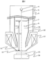
- FIG. 1 is a schematic cross-sectional view showing a scanning electron microscope according to Example 1.
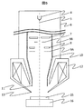
- FIG. 1 is a schematic cross-sectional view showing a scanning electron microscope according to Example 1.
- FIG. 1 is a schematic cross-sectional view showing a scanning electron microscope according to Example 1.
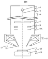
- FIG. 6 is a schematic cross-sectional view showing a scanning electron microscope according to Example 2.
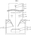
- FIG. 6 is a schematic cross-sectional view showing a scanning electron microscope according to Example 2.
- FIG. 6 is a schematic cross-sectional view showing a scanning electron microscope according to Example 2.
- FIG. 6 is a schematic cross-sectional view showing a scanning electron microscope according to Example 2.
- FIG. 1 is a schematic cross-sectional view showing a scanning electron microscope according to Example 2.
- FIG. 6 is a schematic cross-sectional view showing a scanning electron microscope according to Example 2.
- FIG. 6 is a schematic cross-sectional view showing a scanning electron microscope according to Example 2.
- FIG. 6 is a schematic cross-sectional view showing a scanning electron microscope according to Example 2.
- Examples include an electron source for generating an electron beam to be a probe, an aperture for limiting the diameter of the electron beam, a sample stage on which a sample to be irradiated with the electron beam is mounted, and an object for focusing the electron beam on the sample surface.
- An electron lens including a lens, a deceleration unit that decelerates as the electron beam passes through the objective lens as it approaches the sample, a deflector that scans the electron beam on the sample, and signal electrons emitted from the sample, It has at least two detectors for detecting signal electrons that have passed through the objective lens, the two detectors are arranged between the electron source and the objective lens, and the two sensitive surfaces have an axisymmetric shape with respect to the optical axis.
- One of the detectors is a detector arranged exclusively to detect high-energy signal electrons that have passed through the deceleration electric field type energy filter, and the first detector of the detectors is the first detector.
- the first detector is installed on the sample side of the second detector, and the distance between the sample side tip of the objective lens and the sensitive surface of the first detector is Disclosed is a scanning electron microscope in which L1 / L2 ⁇ 5/9, where L1 is the distance between the tip of the objective lens on the sample side and the sensitive surface of the second detector.
- the embodiment includes a signal processing circuit for linearly adding output signals from the first detector and the second detector.
- the embodiment discloses that the first detector detects backscattered electrons and the second detector detects secondary electrons.
- the embodiment discloses that the deceleration electric field type energy filter is provided as a unit independent of the first detector.
- the embodiment discloses that the deceleration electric field type energy filter is provided as a unit integrated with the first detector.
- a deceleration electric field type energy filter is provided on the sample side from the sensing surface of the second detector, and the first detector and the second detector are separately passed through the deceleration electric field type energy filter. Detecting energetic electrons is disclosed.
- the embodiment discloses that the detection solid angle of the first detector facing from the tip of the objective lens is larger than the detection solid angle of the second detector.
- the detector used for the first detector or the second detector is a semiconductor detector, an avalanche diode, a micro channel plate, a detector using a scintillator material as a component, or a combination thereof. It is disclosed.
- the embodiment includes an electron source that generates an electron beam to be a probe, an aperture that limits the diameter of the electron beam, a sample stage on which a sample to be irradiated with the electron beam is mounted, and the electron beam is focused on the sample surface
- An electron lens including an objective lens, a decelerating means for decelerating as the electron beam passes through the objective lens, a deflector that scans the electron beam on the sample, and a signal electron emitted from the sample
- at least two conversion plates that collide with signal electrons that have passed through the objective lens are provided, the two conversion plates are arranged between the electron source and the objective lens, and the collision surfaces of the two conversion plates are aligned with respect to the optical axis.
- One of the conversion plates has a symmetric shape, and the first conversion plate and the first conversion plate are arranged such that high-energy signal electrons that have passed through the deceleration electric field type energy filter collide exclusively. What is 1 conversion board? When the other conversion plate is the second conversion plate, the first conversion plate is placed closer to the sample side than the second conversion plate, and the front surface of the objective lens on the sample side and the collision surface of the first conversion plate A scanning electron microscope in which L1 / L2 ⁇ 5/9 is disclosed, where L1 is a distance between and L2 is a distance between the tip of the objective lens on the sample side and the collision surface of the second conversion plate.
- the embodiment includes a sensitive surface for detecting conversion electrons emitted from the collision surface to the sample side by the signal electrons colliding with the first conversion plate, and is arranged symmetrically with respect to the optical axis outside the optical axis. And a sensing surface for detecting conversion electrons emitted from the collision surface to the sample side by the signal electrons colliding with the second conversion plate. It is disclosed that the third and fourth detectors are arranged symmetrically with respect to the axis. Also disclosed is a signal processing circuit for linearly adding the output signals from the first, second, third, and fourth detectors.
- the embodiment discloses detecting conversion electrons generated by collision of backscattered electrons with the first conversion plate and detecting conversion electrons generated by collision of secondary electrons with the second conversion plate. .
- the embodiment discloses that the deceleration electric field type energy filter is provided as a unit independent of the first conversion plate.
- the embodiment discloses that the deceleration electric field type energy filter is provided as a unit integrated with the first conversion plate.
- a deceleration electric field type energy filter is provided on the sample side from the collision surface of the second conversion plate, and each of the first conversion plate and the second conversion plate separately passes through the deceleration electric field type energy filter. Disclose that energy electrons collide.
- the embodiment discloses that the collision solid angle of the first conversion plate facing from the tip of the objective lens is larger than the collision solid angle of the second conversion plate.
- the embodiments disclose that the detectors used in the first, second, third, and fourth detectors are detectors that use scintillator material as a component or a combination thereof.
- the embodiment discloses that the material having an atomic number of 50 or more is included in the collision surfaces of the first and second conversion plates.
- a material having a negative electron affinity is included in the collision surfaces of the first and second conversion plates.
- FIG. 2 is a conceptual diagram of the overall configuration of the scanning electron microscope according to the present embodiment.
- the scanning electron microscope shown in FIG. 2 roughly includes an electron gun 4 having a mechanism for irradiating a sample 15 with an irradiation electron beam, an aperture for limiting the diameter of the irradiation electron beam, a condenser lens, and an objective lens.
- An electron lens such as a detector for detecting secondary electrons 2, a detector for detecting backscattered electrons 3, an energy filter 9 A for shielding secondary electrons 2, a deflector, and a sample 15. It has a sample stage 16 and its mechanism, a display device for SEM images, a controller for controlling the entire SEM, and an evacuation facility for locating and observing the observation area.
- each signal electron on the detector sensing surface depends on the deflection field formed on the signal electron trajectory, but the signal electron trajectory accelerated by the deceleration optical system is essentially the deflection field. You can think of it as position independent. For this reason, the deflector installation position is arbitrary in this embodiment.
- FIG. 2 shows the position of the sensitive surface of the detector for detecting secondary electrons and backscattered electrons as the sensitive surface 7 of the second detector and the sensitive surface 8 of the first detector, respectively.
- the sensitive surface 8 of the first detector for detecting backscattered electrons is installed closer to the sample 15 than the sensitive surface 7 of the second detector for detecting secondary electrons. .
- the electron gun 4 corresponds to any of various electron guns such as CFE (Cold Field Emission), SE (Schottky Emission), and thermionic Emission.
- CFE Cold Field Emission
- SE Schottky Emission
- thermionic Emission The electron gun mounted on the scanning electron microscope is selected from these according to the desired apparatus performance.
- the objective lens of the scanning electron microscope shown in this embodiment is an out-lens type with a small leakage magnetic field with respect to the sample 15, and the cylindrical electrode 10 is installed along the inner wall of the magnetic path of the objective lens of the scanning electron microscope.
- the cylindrical electrode 10 is set at a higher potential than the objective lens magnetic path 12. Thereby, a decelerating electric field for the irradiation electron beam is formed between the sample side end 12 of the cylindrical electrode and the sample side end 13 of the objective lens magnetic path, and gradually decelerated when the irradiation electron beam passes. It has become.
- the potential difference between the objective lens magnetic path 12 and the sample 15 is set within 1 kV.
- the cylindrical electrode 10 and the objective lens magnetic path 12, and the gap between the cylindrical electrode 10 and the SEM barrel 6 are configured to be electrically insulated by an insulator (not shown).
- the cylindrical electrode 10 made of a magnetic material is used as a part of the objective lens magnetic path 12 as shown in FIG.
- the cylindrical electrode 10 and the objective lens 12 are configured to be electrically insulated from each other by an insulator (not shown) as long as they are magnetically coupled.
- the cylindrical electrode 10 needs to be at a high potential with respect to the sample 15 in order to form a deceleration electric field.
- This potential difference is set to Vd.
- Vd is set to about 10 kV.
- the distance (WD) between the sample 15 and the sample side end portion 13 (tip end portion) of the objective lens magnetic path is set to 10 mm or less. It is desirable.
- the acceleration-deceleration method in which the sample is grounded and the light source side is higher than that is the same as the method called the deceleration method in which the objective lens is grounded and the sample is a negative potential. If the potential distribution is the same, the same electric field lens action can be obtained. For this reason, hereinafter, the acceleration-deceleration method and the deceleration method will be unified and described as the deceleration method without distinguishing between them.
- a part of the signal electrons 1 generated in the sample 15 is caused by the electric field formed between the sample side end 11 of the cylindrical electrode 10 and the objective lens magnetic path end 13 and the objective lens 12. It is converged by the formed magnetic field, accelerated by the electric field, and proceeds in the direction opposite to the irradiation electron beam.
- the sensitive surface 8 of the first detector and the sensitive surface 7 of the second detector are both arranged symmetrically with respect to the optical axis and have the same potential as the cylindrical electrode 10.
- Vd there is a potential difference Vd between the sample 15 and the sensitive surface 8 of the first detector and the sensitive surface 7 of the second detector, and some of the signal electrons generated in the sample 15 are generated by the first detector. It reaches the sensing surface 8 or the sensing surface 7 of the second detector with an acceleration of about 10 KV. This is sufficient energy for detection with an existing electron detector.
- the first detector and the second detector those capable of achieving the illustrated arrangement of the sensing surface and capable of detecting the signal electrons accelerated by the potential difference Vd are used.
- a semiconductor detector, an avalanche diode, a micro channel plate, a detector using a scintillator material as a constituent element, and the like can be considered, and any type of detector may be used. If there is no problem in linear addition of signals described later, different types of detectors may be used for the first detector and the second detector.
- a detector using a scintillator material is typically installed on the sensitive surface from the viewpoint of multiplication factor and responsiveness.
- signal electrons are detected on the same principle as an Everhart & Thornley type (hereinafter referred to as ET type) detector generally used as a detector of a scanning electron microscope. it can.
- ET type Everhart & Thornley type
- This detector includes a scintillator that converts accelerated signal electrons into light, and a photomultiplier tube that converts light into photoelectrons and amplifies the photoelectrons, and the scintillator and photomultiplier tubes are connected by a light guide.
- the scintillator emits sufficient light if the incident signal electrons have an energy higher than 5 keV or more, and guides this light to the sensitive surface of the photomultiplier tube via the light guide, thereby causing the signal electrons 1 Can be detected as an electrical signal. Since the scintillator is an insulator, charging occurs when signal electrons collide, and in some cases, the scintillator may be decelerated immediately before reaching the sensitive surface. In order to avoid this, it is desirable to coat the surface of the scintillator by depositing a conductor such as Al. This metal coating also has an effect of reflecting light generated by the scintillator to the photomultiplier tube side without leaking to the outside.
- the sensitive surface 8 of the first detector and the sensitive surface 7 of the second detector shown in FIG. 2 are synonymous with the conductor surface that covers the scintillator surface. In this case, the conductor on the scintillator surface and the cylindrical electrode 10 have the same potential.
- the conversion electrode is regarded as the sensitive surface of the first detector or the second detector, and the conversion electrode has the same potential as the cylindrical electrode 10.
- the conversion electrode In the case of a method in which the conversion electrode is detected by an off-axis detector, the number of converted electrons reaching the detector sensing surface changes depending on the distance between the conversion electron generation site and the off-axis detector, which is the cause of shading. There is a possibility. Therefore, as shown in FIG. 4, the first detectors 18A and 18B for detecting the converted electrons off-axis and the second detectors 17A and 17B for detecting the converted electrons are arranged symmetrically with respect to the optical axis. By installing at, shading can be avoided in low magnification observation. In this case, it is expected that an SEM image with reduced shading can be obtained by linearly adding the output signals of two detectors arranged symmetrically with respect to the optical axis.
- the surface portion of the conversion electrode is preferably made of a material having a large amount of secondary electron emission.
- a metal film such as gold (Au, atomic number 79) is used.
- a film made of a material having a larger amount of secondary electron emission than a normal metal, such as magnesium oxide or diamond having a high electron affinity, may be used.
- the first detector and the second detector are the same type of detector, backscattered electrons 3 and secondary electrons 2 flying on the detector sensing surface are detected. For this reason, when the backscattered electrons 3 are detected without detecting the secondary electrons 2 by the first detector, it is necessary to install an energy filter 9A in front of the sensitive surface 8 of the first detector.
- the energy filter 9A may be installed as a component integrated with the first detector, but may be installed as a component separate from the first detector. However, in the case of installation as a separate structure, all the signal electrons 1 that reach the sensitive surface 8 of the first detector always pass through the energy filter 9A before reaching the sensitive surface 8 of the first detector. Need to be placed in. A configuration that does not affect the trajectory of the irradiated electron beam due to a change in the electric field outside the energy filter accompanying the on / off of the filter is desirable.
- the trajectory of the signal electrons 1 depends on the electric field formed between the sample side end 11 of the cylindrical electrode and the sample side end 13 of the objective lens magnetic path and the magnetic field formed by the objective lens 12. For this reason, when the position of the sample 15 and the irradiation voltage of the irradiation electron beam are changed, the excitation necessary for focusing the irradiation electron beam on the surface of the sample 15 changes, and the trajectory of the signal electron 1 also changes accordingly. Since the electric field and magnetic field of the objective lens are controlled to focus the irradiation electron beam, the electric field and magnetic field cannot be controlled to control the trajectory of the signal electrons 1.
- the observation conditions such as acceleration voltage and WD are changed in various ways. Therefore, the first detector and the second detector assume that the secondary electrons 2 and the backscattered electrons 3 are mixed and detected depending on the observation conditions.
- the amount of secondary electrons 2 emitted according to the energy distribution of FIG. 1 is sufficiently larger than the backscattered electrons 3. Image quality close to an electronic image can be obtained.
- an energy filter 9A is required.
- the SEM image of the low magnification is displayed for the same reason as the electron source side detector of Patent Document 1.
- a shading that darkens is observed.
- the energy filter 9A is turned off, and the signal electrons 1 are detected by the first detector and the second detector.
- the influence of shading can be reduced by linearly adding the signals of both detectors and displaying them as an SEM image.
- the signals detected by the two detectors are displayed as SEM images, the amount of signal increases compared to the case where the detection signal of the second detector alone is displayed as an SEM image, and the S / N is high. SEM images of secondary electrons are expected to be obtained.
- the signal electrons generated in the vicinity of the optical axis are subjected to the convergence effect from the objective lens, so the off-axis is relatively small. For this reason, most of the signal electrons generated near the optical axis pass through the central hole of the first detector and are detected by the second detector. As shown in FIG. 2, the first detector and the second detector are each provided with an electron passage hole in the center. For this reason, some of the signal electrons generated near the optical axis that should be detected by the second detector pass through the central hole of the second detector and are not detected. In order to effectively reduce the number of signal electrons passing through the center hole, a configuration in which the sensitive surface of the second detector installed on the electron source side is set at a position away from the sample, that is, a configuration with a large L2 is used. desirable.
- L1 / L2 in terms of the configuration of the detector, a structure in which L1 / L2 is as small as possible is desirable, but the value of L1 / L2 is restricted by the arrangement of the objective lens and condenser lens constituting the optical system. Since both the first detector and the second detector are installed between the objective lens and the electron source, the position of the sensitive surface of the first detector depends on the size and structure of the objective lens and the energy filter, and is unlimited. Cannot be installed near the sample. Further, when considering the arrangement of the components of the optical system for use by changing the acceleration voltage or WD, the position of the sensitive surface of the second detector cannot be placed at an unlimited distance from the sample.
- an energy filter 9B is provided separately from the first detector as shown in FIG. .
- a configuration is adopted in which all signal electrons 1 that reach the sensitive surface 7 of the second detector are arranged so as to pass through the energy filter 9B before reaching the sensitive surface 7 of the second detector.
- a SEM image of linearly added signals of the first detector and the second detector is displayed with both the energy filter 9A of the detector and the energy filter 9B of the second detector turned on, and an SEM image of backscattered electrons is obtained without shading. It becomes possible to do.
- the second order is used for the above reason.
- Electronic SEM images can be obtained without shading, and SEM images with a wide range of magnification can be provided for energy-selected SEM images.
- the filter voltages can be set to different filter voltages.
- FIG. 6 shows a conceptual diagram of the overall configuration of the scanning electron microscope of the present embodiment. Hereinafter, the difference from the first embodiment will be mainly described.
- the scanning electron microscope shown in FIG. 6 roughly includes an electron gun 4, an aperture, a condenser lens, an objective lens, a second detector, a first detector, an energy filter 9A, a deflector, a sample 15, a sample stage 16, and its It has a mechanism, a SEM image display device, a controller that controls the entire SEM, and a vacuum exhaust system.
- the scanning electron microscope shown in FIG. 6 differs from Example 1 in the type of objective lens.
- the objective lens of this embodiment is a semi-in-lens type objective lens that intentionally leaks a magnetic field to the sample. Compared with the configuration of the first embodiment, higher resolution can be obtained.
- the principle that the influence of shading can be reduced with the SEM image obtained by adding the output signals of the first detector and the second detector is the same as in the first embodiment.
- the sample-side end 13 of the objective lens magnetic path is at a higher potential than the sample 15.
- This potential difference is set to Vd as in the first embodiment.
- Vd is set in the range of 1 to 5 kV.
- the detector is an ET type detector, the scintillator does not emit light. Therefore, the sensitive surface 7 of the first detector and the sensitive surface 8 of the second detector are more independent of the objective lens 12 than the sample 15. It is desirable to set a high potential of about 10 kV.
- the sensitive surface 7 of the first detector and the sensitive surface 8 of the second detector have the same potential as the objective lens magnetic path 12. There is no hindrance.
- an electrode 14 for controlling the electric field may be separately provided on the sample side of the lower magnetic path of the objective lens 12.
- the electrode 14 needs to be a nonmagnetic material.
- the potential difference between the electrode 14 and the sample 15 is preferably set within 1 KV.
- a cylindrical electrode 10 containing the first detector and the second detector may be provided.
- the potential difference between the sample-side end 11 of the cylindrical electrode and the electric field control electrode 14 is configured to be Vd.
- the cylindrical electrode 10 is made of a magnetic material.
Landscapes
- Chemical & Material Sciences (AREA)
- Analytical Chemistry (AREA)
- Analysing Materials By The Use Of Radiation (AREA)
Abstract
Description
2…二次電子
3…後方散乱電子
4…電子銃
5…光軸
6…SEM鏡筒
7…第2検出器の感受面
8…第1検出器の感受面
9A…第1検出器で検出される信号電子1に対する減速電界型エネルギーフィルタ
9B…第2検出器で検出される信号電子1に対する減速電界型エネルギーフィルタ
10…筒状電極
11…筒状電極の試料側端部
12…対物レンズ磁路
13…対物レンズ磁路の試料側端部
14…電界制御電極
15…試料
16…試料台
17A…変換電子を検出するための第2検出器A
17B…変換電子を検出するための第2検出器B
18A…変換電子を検出するための第1検出器A
18B…変換電子を検出するための第1検出器B
Claims (19)
- プローブとなる電子線を発生させる電子源と、
前記電子線の径を制限するアパーチャと、
前記電子線が照射される試料を搭載する試料台と、
前記電子線を前記試料表面に収束する対物レンズを含む電子レンズと、
前記電子線が前記対物レンズを通過する際に、前記試料に近づくにつれて減速させる減速手段と、
前記電子線を試料上で走査する偏向器と、
前記試料から放出された信号電子のうち、対物レンズを通過した信号電子を検出する少なくとも2つの検出器を備え、
前記2つ検出器は前記電子源と前記対物レンズとの間に配置され、
前記2つの感受面は光軸に対し軸対称な形状を持ち、
前記検出器のうちの1つは、減速電界型エネルギーフィルタを通過した高エネルギーの信号電子を専ら検出するように配置された検出器を第1検出器、前記検出器のうち第1検出器とは異なる、もう1つの検出器を第2検出器とした場合に、前記第1検出器が前記第2検出器よりも試料側に設置され、
前記対物レンズの前記試料側の先端部と前記第1検出器の感受面の間の距離をL1、前記対物レンズの前記試料側の先端部と前記第2検出器の感受面の間の距離をL2として、L1/L2≦5/9であることを特徴とする走査電子顕微鏡。 - 請求項1に記載の走査電子顕微鏡において、
前記第1検出器および前記第2検出器からの出力信号を線形加算するための信号処理回路を備えることを特徴とする走査電子顕微鏡。 - 請求項1に記載の走査電子顕微鏡において、
前記第1検出器が後方散乱電子を検出し、前記第2検出器で二次電子を検出することを特徴とする走査電子顕微鏡。 - 請求項1に記載の走査電子顕微鏡において、
前記減速電界型エネルギーフィルタは、前記第1検出器とは独立したユニットとして具備されていることを特徴とする走査電子顕微鏡。 - 請求項1に記載の走査電子顕微鏡において、
前記減速電界型エネルギーフィルタは、前記第1検出器と一体のユニットとして具備されていることを特徴とする走査電子顕微鏡。 - 請求項1に記載の走査電子顕微鏡において、
前記第2検出器の感受面より前記試料側に減速電界型エネルギーフィルタが具備され、
前記第1検出器および前記第2検出器について、各々別々に前記減速電界型エネルギーフィルタを通過した高エネルギー電子を検出することを特徴とする走査電子顕微鏡。 - 請求項1に記載の走査電子顕微鏡において、
対物レンズ先端部から臨む第1検出器の検出立体角が、第2検出器の検出立体角よりも大きいことを特徴とする走査電子顕微鏡。 - 請求項1に記載の走査電子顕微鏡において、
第1検出器または第2検出器に用いられる検出器が、半導体検出器、アバランシェダイオード、マイクロ・チャンネル・プレート、もしくは構成要素としてシンチレータ材料を用いる検出器またはそれらの組み合わせであることを特徴とする走査電子顕微鏡。 - プローブとなる電子線を発生させる電子源と、
前記電子線の径を制限するアパーチャと、
前記電子線が照射される試料を搭載する試料台と、
前記電子線を前記試料表面に収束する対物レンズを含む電子レンズと、
前記電子線が前記対物レンズを通過する際に、前記試料に近づくにつれて減速させる減速手段と、
前記電子線を試料上で走査する偏向器と、
前記試料から放出された信号電子のうち、対物レンズを通過した信号電子が衝突する少なくとも2つの変換板を備え、
前記2つの変換板は前記電子源と前記対物レンズとの間に配置され、
前記2つの変換板の衝突面は光軸に対し軸対称な形状を持ち、
前記変換板のうちの1つは、減速電界型エネルギーフィルタを通過した高エネルギーの信号電子が専ら衝突するように配置された変換板を第1変換板、前記変換板のうち第1変換板とは異なる、もう1つの変換板を第2変換板とした場合に、前記第1変換板が前記第2変換板よりも試料側に設置され、
前記対物レンズの前記試料側の先端部と前記第1変換板の衝突面の間の距離をL1、前記対物レンズの前記試料側の先端部と前記第2変換板の衝突面の間の距離をL2として、L1/L2≦5/9であることを特徴とする走査電子顕微鏡。 - 請求項9に記載の走査電子顕微鏡において、
前記第1変換板に衝突した信号電子によって、前記衝突面から前記試料側に放出される変換電子を検出する感受面を備え、前記光軸外に、前記光軸を基準に対称に配置された第1、第2の検出器を具備し、
前記第2変換板に衝突した信号電子によって、前記衝突面から前記試料側に放出される変換電子を検出する感受面を備え、前記光軸外に、前記光軸を基準対称に配置された、第3、第4の検出器を具備したことを特徴とする走査電子顕微鏡。 - 請求項10に記載の走査電子顕微鏡において、
前記第1、第2、第3、および第4の検出器からの出力信号を線形加算するための信号処理回路を備えることを特徴とする走査電子顕微鏡。 - 請求項9に記載の走査電子顕微鏡において、
前記第1変換板に後方散乱電子が衝突して発生する変換電子を検出し、前記第2変換板に二次電子が衝突して発生する変換電子を検出することを特徴とする走査電子顕微鏡。 - 請求項9に記載の走査電子顕微鏡において、
前記減速電界型エネルギーフィルタは、前記第1変換板とは独立したユニットとして具備されていることを特徴とする走査電子顕微鏡。 - 請求項9に記載の走査電子顕微鏡において、
前記減速電界型エネルギーフィルタは、前記第1変換板と一体のユニットとして具備されていることを特徴とする走査電子顕微鏡。 - 請求項9に記載の走査電子顕微鏡において、
前記第2変換板の衝突面より前記試料側に減速電界型エネルギーフィルタが具備され、
前記第1変換板および前記第2変換板について、各々別々に前記減速電界型エネルギーフィルタを通過した高エネルギー電子が衝突することを特徴とする走査電子顕微鏡。 - 請求項9に記載の走査電子顕微鏡において、
対物レンズ先端部から臨む第1変換板の衝突立体角が、第2変換板の衝突立体角よりも大きいことを特徴とする走査電子顕微鏡。 - 請求項9記載の走査電子顕微鏡において、
第1、第2、第3、および第4検出器に用いられる検出器が、構成要素としてシンチレータ材料を用いる検出器またはそれらの組み合わせであることを特徴とする走査電子顕微鏡。 - 請求項9記載の走査電子顕微鏡において、
第1、第2変換板の衝突面に、原子番号50以上の材料が含まれることを特徴とする走査電子顕微鏡。 - 請求項9記載の走査電子顕微鏡において、
第1、第2変換板の衝突面に、負の電子親和力を有する材料が含まれることを特徴とする走査電子顕微鏡。
Priority Applications (4)
| Application Number | Priority Date | Filing Date | Title |
|---|---|---|---|
| CN201480036932.XA CN105340051B (zh) | 2013-08-02 | 2014-07-11 | 扫描电子显微镜 |
| JP2015529496A JP6177915B2 (ja) | 2013-08-02 | 2014-07-11 | 走査電子顕微鏡 |
| US14/899,795 US9536703B2 (en) | 2013-08-02 | 2014-07-11 | Scanning electron microscope |
| DE112014002951.3T DE112014002951B4 (de) | 2013-08-02 | 2014-07-11 | Rasterelektronenmikroskop |
Applications Claiming Priority (2)
| Application Number | Priority Date | Filing Date | Title |
|---|---|---|---|
| JP2013160930 | 2013-08-02 | ||
| JP2013-160930 | 2013-08-02 |
Publications (1)
| Publication Number | Publication Date |
|---|---|
| WO2015016040A1 true WO2015016040A1 (ja) | 2015-02-05 |
Family
ID=52431580
Family Applications (1)
| Application Number | Title | Priority Date | Filing Date |
|---|---|---|---|
| PCT/JP2014/068529 Ceased WO2015016040A1 (ja) | 2013-08-02 | 2014-07-11 | 走査電子顕微鏡 |
Country Status (5)
| Country | Link |
|---|---|
| US (1) | US9536703B2 (ja) |
| JP (1) | JP6177915B2 (ja) |
| CN (1) | CN105340051B (ja) |
| DE (1) | DE112014002951B4 (ja) |
| WO (1) | WO2015016040A1 (ja) |
Cited By (3)
| Publication number | Priority date | Publication date | Assignee | Title |
|---|---|---|---|---|
| WO2019193624A1 (ja) * | 2018-04-02 | 2019-10-10 | 株式会社日立ハイテクノロジーズ | 電子顕微鏡 |
| WO2019224896A1 (ja) * | 2018-05-22 | 2019-11-28 | 株式会社日立ハイテクノロジーズ | 荷電粒子線装置及び荷電粒子線装置の検出器位置調整方法 |
| KR20210102988A (ko) * | 2019-01-08 | 2021-08-20 | 어플라이드 머티리얼즈 이스라엘 리미티드 | 주사 전자 현미경 및 오버레이 모니터링을 위한 방법 |
Families Citing this family (20)
| Publication number | Priority date | Publication date | Assignee | Title |
|---|---|---|---|---|
| WO2016084157A1 (ja) * | 2014-11-26 | 2016-06-02 | 株式会社日立製作所 | 走査電子顕微鏡およびその電子軌道調整方法 |
| DE112015006104B4 (de) * | 2015-03-25 | 2022-05-19 | Hitachi High-Tech Corporation | Elektronenmikroskop |
| DE112016006965B4 (de) * | 2016-07-28 | 2022-05-25 | Hitachi High-Tech Corporation | Ladungsträgerstrahlvorrichtung |
| JP6718782B2 (ja) * | 2016-09-21 | 2020-07-08 | 日本電子株式会社 | 対物レンズおよび透過電子顕微鏡 |
| JP2018147764A (ja) * | 2017-03-07 | 2018-09-20 | 日本電子株式会社 | 走査電子顕微鏡 |
| CN110662618A (zh) * | 2017-03-31 | 2020-01-07 | 阿尔卡姆公司 | 形成三维物品的方法和设备 |
| JP6929760B2 (ja) * | 2017-11-07 | 2021-09-01 | キヤノン株式会社 | 電子線検出素子、電子顕微鏡、透過型電子顕微鏡 |
| JP7228869B2 (ja) * | 2018-02-23 | 2023-02-27 | 国立大学法人 東京大学 | 電子顕微鏡及び測定試料の観察方法 |
| US11037753B2 (en) * | 2018-07-03 | 2021-06-15 | Kla Corporation | Magnetically microfocused electron emission source |
| JP7008650B2 (ja) * | 2019-02-01 | 2022-01-25 | 日本電子株式会社 | 荷電粒子線システム及び走査電子顕微鏡を用いた試料測定方法 |
| WO2021038754A1 (ja) | 2019-08-28 | 2021-03-04 | 株式会社日立ハイテク | イオンガン及びイオンミリング装置 |
| JP7148467B2 (ja) * | 2019-08-30 | 2022-10-05 | 株式会社日立ハイテク | 荷電粒子線装置 |
| DE102019214879A1 (de) * | 2019-09-27 | 2021-04-01 | Carl Zeiss Microscopy Gmbh | Verfahren zum Reduzieren topologischer Artefakte in EDS-Analysen |
| DE102019133658A1 (de) * | 2019-12-10 | 2021-06-10 | Carl Zeiss Smt Gmbh | Vorrichtung und Verfahren zum Bearbeiten einer mikrostrukturierten Komponente |
| JP7307770B2 (ja) * | 2021-07-20 | 2023-07-12 | 日本電子株式会社 | 分析装置および画像処理方法 |
| KR20230068893A (ko) | 2021-11-11 | 2023-05-18 | 삼성전자주식회사 | 주사 전자 현미경(Scannig Electron Microscope, 이하 SEM), SEM을 동작시키는 방법 및 이를 이용한 반도체 소자를 제조하는 방법 |
| CN115732298A (zh) * | 2022-11-23 | 2023-03-03 | 国仪量子(合肥)技术有限公司 | 扫描电子显微镜 |
| DE102024109805B4 (de) | 2024-04-09 | 2025-11-27 | Carl Zeiss Microscopy Gmbh | Verfahren zum Betreiben eines Teilchenstrahlmikroskops, Teilchenstrahlmikroskop und Computerprogrammprodukt |
| CN118098914B (zh) * | 2024-04-23 | 2024-08-27 | 国仪量子技术(合肥)股份有限公司 | 电子探测装置和扫描电镜 |
| KR20250166833A (ko) | 2024-04-23 | 2025-11-28 | 씨아이큐텍 컴퍼니 리미티드 | 전자 검출장치 및 주사전자현미경 |
Citations (6)
| Publication number | Priority date | Publication date | Assignee | Title |
|---|---|---|---|---|
| JPH11242941A (ja) * | 1998-10-07 | 1999-09-07 | Hitachi Ltd | 走査電子顕微鏡 |
| JP2000299078A (ja) * | 1999-04-13 | 2000-10-24 | Topcon Corp | 走査型電子顕微鏡 |
| WO2001075929A1 (fr) * | 2000-03-31 | 2001-10-11 | Hitachi, Ltd. | Microscope electronique a balayage |
| JP2008027737A (ja) * | 2006-07-21 | 2008-02-07 | Hitachi High-Technologies Corp | パターン検査・計測装置 |
| JP2012015130A (ja) * | 2003-01-16 | 2012-01-19 | Carl Zeiss Nts Gmbh | 電子ビーム装置 |
| JP2013089514A (ja) * | 2011-10-20 | 2013-05-13 | Hitachi High-Technologies Corp | 走査電子顕微鏡 |
Family Cites Families (12)
| Publication number | Priority date | Publication date | Assignee | Title |
|---|---|---|---|---|
| JPS59184440A (ja) * | 1983-04-04 | 1984-10-19 | Hitachi Ltd | 走査電子顕微鏡 |
| JP3434165B2 (ja) * | 1997-04-18 | 2003-08-04 | 株式会社日立製作所 | 走査電子顕微鏡 |
| JPH1167139A (ja) * | 1997-08-25 | 1999-03-09 | Hitachi Ltd | 走査電子顕微鏡 |
| WO1999050651A1 (fr) * | 1998-03-27 | 1999-10-07 | Hitachi, Ltd. | Dispositif de verification de motifs |
| DE19828476A1 (de) | 1998-06-26 | 1999-12-30 | Leo Elektronenmikroskopie Gmbh | Teilchenstrahlgerät |
| US6642520B2 (en) | 1999-04-13 | 2003-11-04 | Kabushiki Kaisha Topcon | Scanning electron microscope |
| EP1605492B1 (en) * | 2004-06-11 | 2015-11-18 | ICT Integrated Circuit Testing Gesellschaft für Halbleiterprüftechnik mbH | Charged particle beam device with retarding field analyzer |
| JP4732917B2 (ja) * | 2006-02-15 | 2011-07-27 | 株式会社日立ハイテクノロジーズ | 走査型電子顕微鏡及び欠陥検出装置 |
| DE102006043895B9 (de) | 2006-09-19 | 2012-02-09 | Carl Zeiss Nts Gmbh | Elektronenmikroskop zum Inspizieren und Bearbeiten eines Objekts mit miniaturisierten Strukturen |
| CN101388317B (zh) * | 2008-03-21 | 2010-08-25 | 汉民微测科技(北京)有限公司 | 扫描电子显微镜 |
| JP5097642B2 (ja) * | 2008-08-08 | 2012-12-12 | 株式会社日立ハイテクノロジーズ | 走査形電子顕微鏡 |
| DE102011080341A1 (de) | 2011-08-03 | 2013-02-07 | Carl Zeiss Nts Gmbh | Verfahren und Teilchenstrahlgerät zur Erzeugung eines Bildes eines Objekts |
-
2014
- 2014-07-11 CN CN201480036932.XA patent/CN105340051B/zh active Active
- 2014-07-11 WO PCT/JP2014/068529 patent/WO2015016040A1/ja not_active Ceased
- 2014-07-11 US US14/899,795 patent/US9536703B2/en active Active
- 2014-07-11 JP JP2015529496A patent/JP6177915B2/ja active Active
- 2014-07-11 DE DE112014002951.3T patent/DE112014002951B4/de active Active
Patent Citations (6)
| Publication number | Priority date | Publication date | Assignee | Title |
|---|---|---|---|---|
| JPH11242941A (ja) * | 1998-10-07 | 1999-09-07 | Hitachi Ltd | 走査電子顕微鏡 |
| JP2000299078A (ja) * | 1999-04-13 | 2000-10-24 | Topcon Corp | 走査型電子顕微鏡 |
| WO2001075929A1 (fr) * | 2000-03-31 | 2001-10-11 | Hitachi, Ltd. | Microscope electronique a balayage |
| JP2012015130A (ja) * | 2003-01-16 | 2012-01-19 | Carl Zeiss Nts Gmbh | 電子ビーム装置 |
| JP2008027737A (ja) * | 2006-07-21 | 2008-02-07 | Hitachi High-Technologies Corp | パターン検査・計測装置 |
| JP2013089514A (ja) * | 2011-10-20 | 2013-05-13 | Hitachi High-Technologies Corp | 走査電子顕微鏡 |
Cited By (8)
| Publication number | Priority date | Publication date | Assignee | Title |
|---|---|---|---|---|
| WO2019193624A1 (ja) * | 2018-04-02 | 2019-10-10 | 株式会社日立ハイテクノロジーズ | 電子顕微鏡 |
| JPWO2019193624A1 (ja) * | 2018-04-02 | 2021-03-18 | 株式会社日立ハイテク | 電子顕微鏡 |
| WO2019224896A1 (ja) * | 2018-05-22 | 2019-11-28 | 株式会社日立ハイテクノロジーズ | 荷電粒子線装置及び荷電粒子線装置の検出器位置調整方法 |
| JPWO2019224896A1 (ja) * | 2018-05-22 | 2021-05-20 | 株式会社日立ハイテク | 荷電粒子線装置及び荷電粒子線装置の検出器位置調整方法 |
| US11342155B2 (en) | 2018-05-22 | 2022-05-24 | Hitachi High-Tech Corporation | Charged particle beam device and method for adjusting position of detector of charged particle beam device |
| DE112018007498B4 (de) | 2018-05-22 | 2024-11-28 | Hitachi High-Tech Corporation | Ladungsträgerstrahlvorrichtung und Verfahren zum Einstellen der Position eines Detektors einer Ladungsträgerstrahlvorrichtung |
| KR20210102988A (ko) * | 2019-01-08 | 2021-08-20 | 어플라이드 머티리얼즈 이스라엘 리미티드 | 주사 전자 현미경 및 오버레이 모니터링을 위한 방법 |
| KR102800266B1 (ko) | 2019-01-08 | 2025-04-28 | 어플라이드 머티리얼즈 이스라엘 리미티드 | 주사 전자 현미경 및 오버레이 모니터링을 위한 방법 |
Also Published As
| Publication number | Publication date |
|---|---|
| DE112014002951B4 (de) | 2020-08-06 |
| DE112014002951T5 (de) | 2016-03-17 |
| CN105340051A (zh) | 2016-02-17 |
| JPWO2015016040A1 (ja) | 2017-03-02 |
| US9536703B2 (en) | 2017-01-03 |
| JP6177915B2 (ja) | 2017-08-09 |
| CN105340051B (zh) | 2017-03-08 |
| US20160148782A1 (en) | 2016-05-26 |
Similar Documents
| Publication | Publication Date | Title |
|---|---|---|
| JP6177915B2 (ja) | 走査電子顕微鏡 | |
| CN103733299B (zh) | 扫描电子显微镜 | |
| US10777382B2 (en) | Low voltage scanning electron microscope and method for specimen observation | |
| KR101988189B1 (ko) | 하전 입자선 장치 및 주사 전자 현미경 | |
| US7544937B2 (en) | Charged particle beam device for high spatial resolution and multiple perspective imaging | |
| JP3786875B2 (ja) | 帯電粒子ビームデバイスのための対物レンズ | |
| JP4302316B2 (ja) | 走査形電子顕微鏡 | |
| US7425701B2 (en) | Electron-beam device and detector system | |
| US6407387B1 (en) | Particle beam apparatus | |
| JP6736756B2 (ja) | 荷電粒子線装置 | |
| JP6880209B2 (ja) | 走査電子顕微鏡 | |
| US8183526B1 (en) | Mirror monochromator for charged particle beam apparatus | |
| US6730907B1 (en) | Charged particle device | |
| EP2706553B1 (en) | Method of operating a particle beam device | |
| US20170323761A1 (en) | Charged particle detector | |
| WO2008058491A2 (en) | Scanning electron microscope | |
| KR102947950B1 (ko) | 전자 현미경 |
Legal Events
| Date | Code | Title | Description |
|---|---|---|---|
| WWE | Wipo information: entry into national phase |
Ref document number: 201480036932.X Country of ref document: CN |
|
| 121 | Ep: the epo has been informed by wipo that ep was designated in this application |
Ref document number: 14832908 Country of ref document: EP Kind code of ref document: A1 |
|
| WWE | Wipo information: entry into national phase |
Ref document number: 14899795 Country of ref document: US |
|
| ENP | Entry into the national phase |
Ref document number: 2015529496 Country of ref document: JP Kind code of ref document: A |
|
| WWE | Wipo information: entry into national phase |
Ref document number: 112014002951 Country of ref document: DE |
|
| 122 | Ep: pct application non-entry in european phase |
Ref document number: 14832908 Country of ref document: EP Kind code of ref document: A1 |