WO2015015897A1 - 発光装置の製造方法 - Google Patents
発光装置の製造方法 Download PDFInfo
- Publication number
- WO2015015897A1 WO2015015897A1 PCT/JP2014/064903 JP2014064903W WO2015015897A1 WO 2015015897 A1 WO2015015897 A1 WO 2015015897A1 JP 2014064903 W JP2014064903 W JP 2014064903W WO 2015015897 A1 WO2015015897 A1 WO 2015015897A1
- Authority
- WO
- WIPO (PCT)
- Prior art keywords
- substrate
- light
- light emitting
- led chip
- emitting device
- Prior art date
- Legal status (The legal status is an assumption and is not a legal conclusion. Google has not performed a legal analysis and makes no representation as to the accuracy of the status listed.)
- Ceased
Links
Images




Classifications
-
- H—ELECTRICITY
- H05—ELECTRIC TECHNIQUES NOT OTHERWISE PROVIDED FOR
- H05B—ELECTRIC HEATING; ELECTRIC LIGHT SOURCES NOT OTHERWISE PROVIDED FOR; CIRCUIT ARRANGEMENTS FOR ELECTRIC LIGHT SOURCES, IN GENERAL
- H05B33/00—Electroluminescent light sources
- H05B33/10—Apparatus or processes specially adapted to the manufacture of electroluminescent light sources
-
- H—ELECTRICITY
- H10—SEMICONDUCTOR DEVICES; ELECTRIC SOLID-STATE DEVICES NOT OTHERWISE PROVIDED FOR
- H10H—INORGANIC LIGHT-EMITTING SEMICONDUCTOR DEVICES HAVING POTENTIAL BARRIERS
- H10H20/00—Individual inorganic light-emitting semiconductor devices having potential barriers, e.g. light-emitting diodes [LED]
- H10H20/80—Constructional details
- H10H20/83—Electrodes
- H10H20/831—Electrodes characterised by their shape
-
- H—ELECTRICITY
- H10—SEMICONDUCTOR DEVICES; ELECTRIC SOLID-STATE DEVICES NOT OTHERWISE PROVIDED FOR
- H10H—INORGANIC LIGHT-EMITTING SEMICONDUCTOR DEVICES HAVING POTENTIAL BARRIERS
- H10H20/00—Individual inorganic light-emitting semiconductor devices having potential barriers, e.g. light-emitting diodes [LED]
- H10H20/80—Constructional details
- H10H20/84—Coatings, e.g. passivation layers or antireflective coatings
-
- H—ELECTRICITY
- H10—SEMICONDUCTOR DEVICES; ELECTRIC SOLID-STATE DEVICES NOT OTHERWISE PROVIDED FOR
- H10K—ORGANIC ELECTRIC SOLID-STATE DEVICES
- H10K71/00—Manufacture or treatment specially adapted for the organic devices covered by this subclass
- H10K71/50—Forming devices by joining two substrates together, e.g. lamination techniques
-
- H—ELECTRICITY
- H10—SEMICONDUCTOR DEVICES; ELECTRIC SOLID-STATE DEVICES NOT OTHERWISE PROVIDED FOR
- H10K—ORGANIC ELECTRIC SOLID-STATE DEVICES
- H10K71/00—Manufacture or treatment specially adapted for the organic devices covered by this subclass
- H10K71/60—Forming conductive regions or layers, e.g. electrodes
-
- H—ELECTRICITY
- H10—SEMICONDUCTOR DEVICES; ELECTRIC SOLID-STATE DEVICES NOT OTHERWISE PROVIDED FOR
- H10W—GENERIC PACKAGES, INTERCONNECTIONS, CONNECTORS OR OTHER CONSTRUCTIONAL DETAILS OF DEVICES COVERED BY CLASS H10
- H10W72/00—Interconnections or connectors in packages
-
- H—ELECTRICITY
- H10—SEMICONDUCTOR DEVICES; ELECTRIC SOLID-STATE DEVICES NOT OTHERWISE PROVIDED FOR
- H10H—INORGANIC LIGHT-EMITTING SEMICONDUCTOR DEVICES HAVING POTENTIAL BARRIERS
- H10H20/00—Individual inorganic light-emitting semiconductor devices having potential barriers, e.g. light-emitting diodes [LED]
- H10H20/01—Manufacture or treatment
- H10H20/032—Manufacture or treatment of electrodes
-
- H—ELECTRICITY
- H10—SEMICONDUCTOR DEVICES; ELECTRIC SOLID-STATE DEVICES NOT OTHERWISE PROVIDED FOR
- H10H—INORGANIC LIGHT-EMITTING SEMICONDUCTOR DEVICES HAVING POTENTIAL BARRIERS
- H10H20/00—Individual inorganic light-emitting semiconductor devices having potential barriers, e.g. light-emitting diodes [LED]
- H10H20/01—Manufacture or treatment
- H10H20/034—Manufacture or treatment of coatings
-
- H—ELECTRICITY
- H10—SEMICONDUCTOR DEVICES; ELECTRIC SOLID-STATE DEVICES NOT OTHERWISE PROVIDED FOR
- H10H—INORGANIC LIGHT-EMITTING SEMICONDUCTOR DEVICES HAVING POTENTIAL BARRIERS
- H10H20/00—Individual inorganic light-emitting semiconductor devices having potential barriers, e.g. light-emitting diodes [LED]
- H10H20/01—Manufacture or treatment
- H10H20/036—Manufacture or treatment of packages
- H10H20/0362—Manufacture or treatment of packages of encapsulations
-
- H—ELECTRICITY
- H10—SEMICONDUCTOR DEVICES; ELECTRIC SOLID-STATE DEVICES NOT OTHERWISE PROVIDED FOR
- H10K—ORGANIC ELECTRIC SOLID-STATE DEVICES
- H10K71/00—Manufacture or treatment specially adapted for the organic devices covered by this subclass
- H10K71/40—Thermal treatment, e.g. annealing in the presence of a solvent vapour
-
- H—ELECTRICITY
- H10—SEMICONDUCTOR DEVICES; ELECTRIC SOLID-STATE DEVICES NOT OTHERWISE PROVIDED FOR
- H10W—GENERIC PACKAGES, INTERCONNECTIONS, CONNECTORS OR OTHER CONSTRUCTIONAL DETAILS OF DEVICES COVERED BY CLASS H10
- H10W72/00—Interconnections or connectors in packages
- H10W72/01—Manufacture or treatment
- H10W72/0198—Manufacture or treatment batch processes
-
- H—ELECTRICITY
- H10—SEMICONDUCTOR DEVICES; ELECTRIC SOLID-STATE DEVICES NOT OTHERWISE PROVIDED FOR
- H10W—GENERIC PACKAGES, INTERCONNECTIONS, CONNECTORS OR OTHER CONSTRUCTIONAL DETAILS OF DEVICES COVERED BY CLASS H10
- H10W90/00—Package configurations
Definitions
- the present invention relates to a method for manufacturing a light-emitting device in which a light-emitting element such as an inorganic light-emitting element or an organic light-emitting element is provided using a coating method, and particularly relates to a method for manufacturing a light-emitting device that can be easily manufactured.
- a light emitting device using an LED chip has been proposed.
- the LED chip is bonded by die bonding with the electrode facing upward, the electrode of the LED chip and the wiring of the substrate are connected by wire bonding, and mounted on the substrate.
- the LED chip electrode is placed on the lower side, and the substrate is mounted on the substrate using a flip chip method in which the lower electrode and the wiring of the substrate are connected with a conductive material. In this case, it is necessary to adjust the position of the wiring between the LED chip and the substrate. Therefore, a method for mounting the LED chip without positioning has been proposed (for example, see Patent Documents 1 and 2).
- an upper electrode and a lower electrode of an LED chip are each connected to a conductive layer on a conductive sheet using an anisotropic conductive resin, and the periphery of the LED chip includes insulating beads.
- a light emitting device filled with a non-conductive adhesive is described.
- Patent Document 2 describes an illumination device using a diode (eg, see FIGS. 1 to 3) on a substantially hexagonal column (eg, see FIGS. 76 to 79). It is described that a diode having a width of about 10 to 50 microns and a height of about 5 to 25 microns can be used. Patent Document 2 describes that a diode ink in which a diode is dispersed in a solvent is applied using a coating method, and the diode is provided on a conductive layer. Furthermore, it is described that diode ink can be printed on, for example, LED-based lighting devices or other flexible sheets. The diode ink contains a plurality of particles that are substantially chemically inert.
- Patent Document 1 When manufacturing the light-emitting device of Patent Document 1 described above, it is necessary to attach an anisotropic conductive resin to each LED chip, which causes a problem that the manufacturing process becomes complicated. Further, in Patent Document 2 described above, it is necessary to process the diode into a special shape having a substantially hexagonal column shape, which causes a problem that the manufacturing process becomes complicated and the manufacturing cost increases.
- An object of the present invention is to provide a method for manufacturing a light-emitting device that can solve the problems based on the conventional technology and can be easily manufactured.
- the present invention provides a conductive material on both surfaces of a base material on which a plurality of light emitting elements each having a first electrode and a second electrode facing each other are formed. Cutting out the light emitting element together with the first electrode and the second electrode to obtain a light emitting element provided with conductive members of approximately the same size as the first electrode and the second electrode, respectively, Then, a coating liquid is obtained by mixing with an insulating binder, the coating liquid is applied to the first substrate on which the conductive layer is formed, and the coating layer is formed on the first substrate.
- the step of laminating the second substrate on which the conductive layer is formed and the pressure is applied in the laminating direction of the first substrate and the second substrate, and the pressure is applied at a preset temperature.
- a method of manufacturing a light emitting device characterized by comprising a step of holding for a preset time. It is intended.
- the conductive member is preferably transparent.
- an inorganic light emitting element or an organic light emitting element can be used for a light emitting element, for example.
- the light emitting device can be easily manufactured.
- the conductive member provided in the light-emitting element substantially the same size as the first electrode and the second electrode, the amount of light absorbed by the conductive member out of the light emitted from the light-emitting element is reduced. The light emitted from the light emitting element can be used effectively.
- FIG. 1 It is a flowchart which shows the manufacturing method of the light-emitting device of embodiment of this invention.
- (A)-(c) is a typical perspective view which shows the manufacturing method of the LED chip used for the light-emitting device of embodiment of this invention in order of a process. It is a schematic diagram which shows the manufacturing apparatus utilized for manufacture of the light-emitting device of embodiment of this invention.
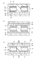
- (A)-(c) is sectional drawing which shows the manufacturing method of the light-emitting device of embodiment of this invention in order of a process. It is sectional drawing which shows the light-emitting device obtained with the manufacturing method of the light-emitting device of embodiment of this invention.
- (A) is a schematic plan view which shows an example of the arrangement state of a light emitting element
- (b) is a schematic plan view which shows the other example of the arrangement state of a light emitting element.
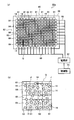
- (A) is a typical top view which shows the other example of the light-emitting device obtained with the manufacturing method of the light-emitting device of embodiment of this invention
- (b) is a principal part enlarged view of Fig.7 (a). is there.
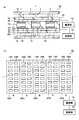
- (A) is sectional drawing which shows the illuminating device using the light-emitting device obtained with the manufacturing method of the light-emitting device of embodiment of this invention
- (b) is the manufacturing method of the light-emitting device of embodiment of this invention. It is a top view which shows the display apparatus using the obtained light-emitting device.
- FIG. 1 is a flowchart showing a method for manufacturing a light emitting device according to an embodiment of the present invention.
- 2 (a) to 2 (c) are schematic perspective views showing a manufacturing method of an LED chip used in the light emitting device according to the embodiment of the present invention in the order of steps.
- an LED chip including an upper electrode and a lower electrode facing each other is used as the light emitting element.
- Each electrode of the LED chip is provided with a conductive member having approximately the same size as the electrode.
- an insulating resin layer is provided between a pair of substrates on which a conductive layer is formed, an LED chip is disposed in the resin layer, and each electrode and each conductive layer are electrically connected via a conductive member. Connected.
- the manufacturing method of the light-emitting device of this embodiment is demonstrated concretely.
- step S10 an LED chip is obtained as a light emitting element (step S10).
- step S10 as shown in FIG. 2A, first, an LED wafer 10 (base material) on which a plurality of LED chips (not shown in FIG. 2A) are formed is prepared.
- the conductive layer 11 is provided on the entire front surface 10a and back surface 10b of the LED wafer 10, respectively.
- the method for forming the conductive layer 11 is not particularly limited.
- the conductive layer 11 may be formed by attaching a conductive sheet, or may be formed by applying a conductive adhesive.
- the conductive layer 11 corresponds to the conductive material of the present invention.
- the configuration of the conductive layer 11 is not particularly limited as long as it has conductivity.
- the conductive layer 11 can be composed of ITO, ZnO, or a conductor containing Ag nanoparticles or Ag nanowires. .
- the conductive layer 11 may be composed of an anisotropic conductive adhesive.
- the conductive layer 11 is preferably transparent, but at least one of the front surface 10a side and the back surface 10b side may be opaque.
- the term “transparent” means that the average transmittance in the emission wavelength range of the light emitting element is preferably 50% or more, more preferably 80% or more, and most preferably 90% or more.
- the emission wavelength range is a range having a light amount of 10% or more of the peak intensity. In the following, even if transparency is not particularly described, transparency is the above-mentioned definition. Opaque means that the above-mentioned transparency is not satisfied.
- the LED wafer 10 is cut out together with the conductive layer 11, and the LED chip 14 shown in FIG. obtain.
- the LED chip 14 is formed with electrodes corresponding to the front surface 10a and the back surface 10b of the LED wafer 10, and the LED chip 14 has an upper electrode 16a and a lower electrode 16b facing each other.
- the LED chip 14 emits light from the upper electrode 16a side and the lower electrode 16b side.
- the conductive member 12 is provided in substantially the same size as each of the upper electrode 16a and the lower electrode 16b.
- the upper electrode 16a corresponds to the first electrode of the present invention
- the lower electrode 16b corresponds to the second electrode of the present invention.
- the obtained LED chip 14 is put into, for example, a binder such as an insulating adhesive and mixed to obtain a coating solution for applying the LED chip 14 to the substrate (step S12).
- a binder such as an insulating adhesive
- the insulating adhesive for example, a thermosetting resin agent, a thermoplastic resin agent, and a synthetic rubber are used.
- a viscosity modifier, a solvent, particles serving as a spacer, particles for improving optical properties, and the like can be appropriately added. Each of the particles serving as the spacer and the particles for improving the optical characteristics may be a filler.
- the content of the LED chip 14 in the coating liquid is an amount corresponding to the area ratio of the LED chip 14 with respect to the substrate.
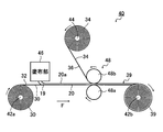
- the manufacturing apparatus 40 is a roll-to-roll apparatus, and includes a rotating shaft 42 a that rolls the first substrate 30 on which the conductive layer 32 is formed, and a second substrate 34 on which the conductive layer 36 is formed.
- a winding shaft 42b is provided for winding the laminated body 39, which is laminated with the first substrate 30 and pressed and heated, into a roll shape.
- the application unit 46 is for applying the above-described application liquid on the conductive layer 32 of the first substrate 30 to form the application film 20.
- the coating liquid 19 for example, slit coating, bar coating, or screen printing is used.
- the roller pair 48 includes rollers 48a and 48b each provided with a heater, and the second substrate 34 is drawn by the roller 48b and is set in advance while being stacked on the first substrate 30 on which the coating film 20 is formed.
- the laminated body 39 is obtained by applying pressure and heat treatment for a predetermined time at the applied pressure and temperature.
- the pressure of the roller 48b with respect to the roller 48a is gradually increased from the initial stage, thereby applying a force in the transport direction F to the LED chip 14 and the upper electrode 16a of the LED chip 14. Can face the conductive layers 32, 36.
- a force in the transport direction F is applied to the LED chip 14 so that the upper electrode 16a of the LED chip 14 faces the conductive layers 32 and 36.
- This control can be made more accurate by installing a plurality of pressure and heating rollers. Since a certain amount of pressure is applied in the wound state, the adhesion can be further increased by further heating.
- the first substrate 30 unwound from the rotating shaft 42a is wound in advance on the winding shaft 42b via the roller pair 48. Then, while winding the first substrate 30 in the transport direction F by the winding shaft 42 b, the coating liquid 19 containing the LED chip 14 and the insulating adhesive 18 is applied from the coating unit 46 to the conductive layer 32 of the first substrate 30.
- the coating film 20 is formed on the conductive layer 32 of the first substrate 30 (see FIG. 4A).
- the LED chip 14 is disposed on the conductive layer 32 of the first substrate 30. At this time, the LED chip 14 is preferably aligned in the direction of the electrodes so that the lower electrode 16b faces the conductive layer 32.
- the direction of the electrodes does not need to be aligned and a mixture of electrodes having different directions is mixed. May be.
- the LED chip 14 can be disposed only by forming the coating film 20 using the coating liquid 19 containing the LED chip 14. Further, when forming the coating film 20, the surface 20 a (see FIG. 3) may be leveled so that the LED chip 14 is oriented so that the lower electrode 16 b of the LED chip 14 faces the conductive layer 32. Thereby, it is suppressed that the electrode of LED chip 14 will be in the state which does not face the conductive layers 32 and 36.
- the roll-shaped second substrate 34 is rewound and placed on the roller 48b of the roller pair 48, and the first substrate 30 is conveyed in the conveying direction F, while the first substrate 30 is shown in FIG.
- the substrate 30 and the second substrate 34 are stacked in the stacking direction C (step S16).
- the rollers 48a and 48b are set to a preset temperature, and at the same time as lamination, pressure is applied in the lamination direction C of the first substrate 30 and the second substrate 34 as shown in FIG.
- heating and pressurizing processes are performed while maintaining a predetermined temperature for a predetermined time (step S18).
- the heating and pressurizing treatment is performed, for example, at a temperature of 150 ° C. for 10 seconds.
- the upper electrode 16 a and the lower electrode 16 b are electrically connected to the conductive layers 32 and 36 according to the direction of the LED chip 14 with respect to the stacking direction C, and between the second substrate 34 and the first substrate 30.
- a resin layer 38 surrounding the periphery of the LED chip 14 is formed, and a laminate 39 is obtained.
- the laminated body 39 is wound up in a roll shape around the winding shaft 42b.
- the laminate 39 is cut to a predetermined size, and as shown in FIG. 5, the power source 52 is connected to the conductive layers 32 and 36, and the controller 54 is further connected to the power source 52 to emit light.
- a device 50 can be obtained.
- the power supply unit 52 applies a voltage to the LED chip 14 through the conductive layers 32 and 36, and can generate a DC voltage or an AC voltage.
- the control unit 54 generates a DC voltage or an AC voltage in the power supply unit 52 and applies the DC voltage or the AC voltage to the LED chip 14. Thereby, the light L can be emitted from the first substrate 30 and the second substrate 34.
- the LED chip 14 is cut out together with the conductive layer 11, thereby The LED chip 14 provided with the conductive member 12 having approximately the same size as the lower electrode 16b can be easily obtained.
- the light emitting device 50 can be easily manufactured by applying the coating solution containing the LED chip 14 to the first substrate 30, and then laminating the second substrate 34, and performing heating and pressure treatment. .
- the conductive member 12 substantially the same size as the upper electrode 16a and the lower electrode 16b, the amount of light absorbed by the conductive member 12 out of the light emitted from the LED chip 14 is reduced, and the LED chip 14 The light emitted from can be effectively used.
- the manufacturing method of a light-emitting device is not limited to a roll-to-roll system, A single wafer type can also be used.
- the heating and pressurizing processes are performed by, for example, using a pair of flat plates to pressurize to a preset pressure sandwiched between the first substrate 30 and the second substrate 34 and the stacking direction C thereof. Heat to set temperature, hold for a preset time, pressurize and heat treatment.
- a coating liquid is prepared and applied.
- the present invention is not limited to this, and an insulating adhesive is applied and LED chips are sprayed thereon. Then, an insulating adhesive may be applied again so as to cover the LED chip 14.
- the light emitting device 50 can be a flexible light emitting device 50 as a whole by making the first substrate 30, the second substrate 34, and the conductive layers 32 and 36 flexible.
- the polarity of the upper electrode 16a and the lower electrode 16b is not particularly limited as long as one is a positive pole and the other is a negative pole.
- the upper electrode 16a and the lower electrode 16b may be transparent or opaque. When opaque, the light is emitted from the side surface side of the LED chip 14. Further, the wavelength of light emitted from the LED chip 14 is not particularly limited.
- the shape of the LED chip 14 is not particularly limited, as shown in FIG. 5, the LED chip 14 has a thickness of T ( ⁇ m) and a width of Y ( ⁇ m). It is preferable that 5 ⁇ Y. In the case of a rectangular parallelepiped, Y is a short width.
- the shape of the LED chip 14 may not be a rectangular parallelepiped, but may be a hexagonal column or an octagonal column. At that time, the width is Y which is the shortest diagonal.
- the distance between the first substrate 30 and the second substrate 34 is K ( ⁇ m), it is preferable that K ⁇ Y. Accordingly, when the second substrate 34 is stacked on the first substrate 30, the LED chip 14 can easily face the upper electrode 16 a and the lower electrode 16 b of the LED chip 14 to the conductive layers 32 and 36.
- the distance K between the substrates is about 10 to 500 ⁇ m.
- the conductive member 12 provided on the LED chip 14 in order to make the upper electrode 16 a and the lower electrode 16 b of the LED chip 14 easily face the conductive layers 32 and 36 when applied, the length of the conductive member 12 in the width direction is set. The length may be longer than the width Y described above.
- the LED chip 14 has been described as an example of the light emitting element.
- the present invention is not limited to this, and an inorganic light emitting element or an organic light emitting element can be used, for example, an inorganic EL chip or an organic EL element.
- a chip can be used.
- the directions of the LED chips 14 with respect to the stacking direction C are uniform, but those having different directions may be mixed.
- the LED chip 14 can emit light by applying an alternating voltage.
- the arrangement of the LED chip 14 is not particularly limited. For example, it is preferable to arrange regularly as shown in FIG. 6A, but may be arranged randomly as shown in FIG. 6B. Even in this case, the LED chips 14 may be aligned in the stacking direction C as described above, or may be mixed in different directions with respect to the stacking direction C.
- the area ratio of the LED chip 14 with respect to the first substrate 30 is, for example, 0.01 to 90%, preferably 0.1 to 50%, and more preferably 1 to 30%.
- both the first substrate 30 and the second substrate 34 are preferably transparent, but are not necessarily transparent, and at least one of them may be opaque. One may be transparent and the rest may reflect light.
- the first substrate 30 and the second substrate 34 are, for example, triacetyl cellulose (TAC), polyethylene terephthalate (PET), polyethylene naphthalate (PEN), syndiotactic polystyrene (SPS), polyphenylene sulfide (PPS), It can be composed of polycarbonate (PC), polyarylate (PAr), polysulfone (PSF), polyester sulfone (PES), polyetherimide (PEI), cyclic polyolefin, polyimide (PI), or the like.
- resin when resin is used for a board
- the conductive layers 32 and 36 are made of, for example, ITO, ZnO, or a conductor containing Ag nanoparticles or Ag nanowires.
- the conductive layers 32 and 36 are preferably transparent, but are not necessarily transparent, and at least one of them may be opaque. Further, the conductive layers 32 and 36 do not cover the entire surface but are partially removed so that light may be transmitted. Further, when the LED chip 14 has sufficient conductivity, the conductive layers 32 and 36 may not be provided.
- the resin layer 38 is made of an insulator as described above, and is in accordance with the composition of a binder such as an insulating adhesive of the coating liquid 19.
- the resin layer 38 may include particles serving as spacers, particles for improving optical characteristics, and the like.
- the resin layer 38 is preferably transparent.
- the light-emitting device manufactured by the present invention is not limited to the light-emitting device 50 shown in FIG. 5, but may have the configuration shown in the light-emitting device 50a shown in FIGS. 7 (a) and 7 (b).
- FIG. 7B is an enlarged view of the region Q in FIG.
- the same components as those of the light emitting device 50 shown in FIG. 5 are denoted by the same reference numerals, and detailed description thereof is omitted.
- the conductive layers 60 and 62 are formed in a strip pattern, and the first substrate 30 and the second substrate 34 are orthogonal to each other between the conductive layer 60 and the conductive layer 62.
- the conductive layer 60 corresponds to the conductive layer 36 of the light emitting device 50
- the conductive layer 62 corresponds to the conductive layer 32 of the light emitting device 50.
- the conductive portion 61 is connected to the power supply portion 52 through the wiring 66
- the conductive layer 62 is connected to the power supply portion 52 in the conductive portion 64 through the wiring 68.
- a voltage is applied to the LED chip 14 between the conductive portion 61 of the conductive layer 60 and the conductive portion 64 of the conductive layer 62 in the stacking direction C (see FIG. 5) of the first substrate 30 and the second substrate 34. Emits light.
- a method generally called a matrix driving method is used, and is located between the conductive portion 61 of the conductive layer 60 and the conductive portion 64 of the conductive layer 62, that is, at the intersection of the conductive portion 61 and the conductive portion 64.
- the LED chip 14 at an arbitrary position can emit light.
- the length of the longest diagonal line of the LED chip 14 is set such that the width between the conductive layers 60 (the width of the region 63 between the conductive portions 61) and the width between the conductive layers 62 (the region 65 between the conductive portions 64) from the viewpoint of suppressing a short circuit. Shorter than the width).
- the arrangement state of the LED chip 14 is not particularly limited as long as the LED chip 14 is arranged on the conductive layers 60 and 62.
- the LED chip 14 may be provided in a region 63 between the conductive portions 61 of the conductive layer 60 and a region 65 between the conductive portions 64 of the conductive layer 62 in the planar direction of the substrate. In this case, since no voltage is supplied to the LED chip 14 that is not between the conductive layer 60 and the conductive layer 62 in the stacking direction of the first substrate 30 and the second substrate 34, no light is emitted.
- the positioning accuracy can be lowered, and the LED chip 14 can be provided simply by applying the coating liquid containing the LED chip 14 as described above.
- the LED chips 14 may be aligned in the stacking direction C or may be mixed in different directions. A DC voltage is applied if all the LED chips 14 are aligned in the stacking direction C, and an AC voltage is applied if the directions are mixed.
- the light-emitting devices 50 and 50a described above can be applied to, for example, the lighting device illustrated in FIG.
- a scattering plate 72 is disposed on the second substrate 34 of the light emitting device 50, and a reflecting plate 74 is disposed below the lower surface 30 b of the first substrate 30 of the light emitting device 50. It has been done.
- the light L emitted to the second substrate 34 side is transmitted through the scattering plate 72 and emitted to the outside by causing the LED chip 14 to emit light, and the light L emitted to the first substrate 30 side is emitted.
- the light is reflected by the reflecting plate 74 toward the second substrate 34 and is emitted from the scattering plate 72 to the outside.
- the scattering plate 72 and the reflection plate 74 known ones can be used as appropriate.
- the scattering plate may also serve as the second substrate 34 and the reflecting plate may serve as the first substrate 30.
- the light emitting device 50a shown in FIG. 7 can be used instead of the light emitting device 50 shown in FIG.
- the LED chip 14 at a specific position can be caused to emit light by the matrix driving method.
- the scattering plate may serve as the second substrate 34 and the reflecting plate may serve as the first substrate 30.
- the light emitting device 50a it is preferable that there are a plurality of LED chips 14 at each intersection J between the conductive portion 61 and the conductive portion 64 as described above (see FIG. 7B).
- the length of the longest diagonal line of the LED chip 14 is also preferably shorter than the width between the conductive layers 60 and the width between the conductive layers 62 from the viewpoint of suppressing a short circuit as described above.
- the flexible lighting device 70 that can be bent can be obtained.
- the flexible lighting device 70 that can be bent is obtained by making the first substrate 30, the second substrate 34, and the conductive layers 60 and 62 flexible. be able to.
- the display device 80 shown in FIG. 8B can be obtained.
- a plurality of LED chips 14R that emit red light are arranged to constitute a red pixel 82R
- a plurality of LED chips 14G that emit green light are arranged to constitute a green pixel 82G
- a plurality of LED chips 14B that emit blue light are arranged.
- a blue pixel 82B is formed.
- the red pixel 82R, the green pixel 82G, and the blue pixel 82B are respectively connected to the power supply unit 52, and when the voltage is applied from the power supply unit 52, the LED chip 14R, the LED chip 14G, and the LED chip 14B emit light in each color.
- control unit 54 controls an image by causing the red pixel 82R, the green pixel 82G, and the blue pixel 82B to emit light at a preset light emission timing for a preset time according to what is displayed.
- LED chip 14R, LED chip 14G, and LED chip 14B are preferably aligned in direction.
- the display device 80 can display an image using a known driving method by arranging the red pixels 82R, the green pixels 82G, and the blue pixels 82B in the same manner as the known display devices. If a pixel is constituted by one light emitting element, pixel display cannot be performed if this light emitting element becomes defective. On the other hand, the display device 80 can be constituted to be one pixel by a plurality of light emitting elements. Defects do not stand out. Further, by increasing the brightness of a pixel in which a defect has occurred in the light emitting element, the same amount of light as that of surrounding pixels can be obtained. Furthermore, by providing a known control circuit composed of TFT elements or the like for each pixel, higher control becomes possible.
- the present invention is basically configured as described above. Although the manufacturing method of the light emitting device of the present invention has been described in detail above, the present invention is not limited to the above-described embodiment, and various improvements or modifications may be made without departing from the gist of the present invention. Of course.
Landscapes
- Engineering & Computer Science (AREA)
- Manufacturing & Machinery (AREA)
- Led Device Packages (AREA)
- Electroluminescent Light Sources (AREA)
- Planar Illumination Modules (AREA)
Abstract
発光装置の製造方法は、対向する第1の電極と第2の電極とを備えた発光素子が複数形成された基材の両面に導電材を設け、基材から導電材と一緒に発光素子を切出し、第1の電極と第2の電極にそれぞれ第1の電極と第2の電極と略同じ大きさの導電部材が設けられた発光素子を得る工程と、発光素子を、絶縁性を有するバインダに混ぜて塗布液を得て、塗布液を導電層が形成された第1の基板に塗布し、塗布層を形成する工程と、第1の基板上に塗布層を挟むようにして、導電層が形成された第2の基板を積層する工程と、第1の基板と第2の基板との積層方向に圧力を印加し、圧力を印加した状態で、予め設定された温度で予め設定された時間保持する工程とを有する。
Description
本発明は、無機発光素子または有機発光素子等の発光素子を塗布法を用いて設けた発光装置の製造方法に関し、特に、容易に製造することができる発光装置の製造方法に関する。
現在、薄型ディスプレイのバックライトユニット、および面状の照明装置等について、薄いものが要求されている。LEDチップを用いた発光装置が提案されている。
従来のLEDチップを用いた発光装置では、LEDチップをダイボンドで電極を上向きにして接着し、ワイヤボンディングでLEDチップの電極と基板の配線とを接続し、基板に実装することがなされている。これ以外に、LEDチップの電極を下側におき、下側の電極と基板の配線を導電性材料で接続するフリップチップ方法を用いて基板に実装することがなされている。この場合、LEDチップと基板の配線の位置を調整する必要がある。
そこで、LEDチップを位置決めすることなく、実装する方法が提案されている(例えば、特許文献1、2参照)。
従来のLEDチップを用いた発光装置では、LEDチップをダイボンドで電極を上向きにして接着し、ワイヤボンディングでLEDチップの電極と基板の配線とを接続し、基板に実装することがなされている。これ以外に、LEDチップの電極を下側におき、下側の電極と基板の配線を導電性材料で接続するフリップチップ方法を用いて基板に実装することがなされている。この場合、LEDチップと基板の配線の位置を調整する必要がある。
そこで、LEDチップを位置決めすることなく、実装する方法が提案されている(例えば、特許文献1、2参照)。
特許文献1には、LEDチップの上部電極と下部電極とが異方性導電性樹脂を用いて、それぞれ導電性シートに導電層に接続されており、LEDチップの周囲が、絶縁ビーズを含んだ非導電性接着剤で満たされている発光装置が記載されている。
特許文献2には、略六角柱上のダイオード(例えば、図1~図3参照)を用いた照明装置が記載されている(例えば、図76~図79参照)。ダイオードとしては、横が約10~50ミクロンで、高さが約5~25ミクロンのものが用いられることが記載されている。
特許文献2では、ダイオードが溶媒に分散したダイオードインクを、塗布法を用いて塗布し、ダイオードを導電層に設けることが記載されている。さらには、ダイオードインクを、例えば、LEDベースの照明装置、または他の可撓性シートに印刷できることが記載されている。なお、ダイオードインクは、実質的に化学的に不活性な複数の粒子が含まれる。
特許文献2では、ダイオードが溶媒に分散したダイオードインクを、塗布法を用いて塗布し、ダイオードを導電層に設けることが記載されている。さらには、ダイオードインクを、例えば、LEDベースの照明装置、または他の可撓性シートに印刷できることが記載されている。なお、ダイオードインクは、実質的に化学的に不活性な複数の粒子が含まれる。
上述の特許文献1の発光装置の製造に際して、異方性導電性樹脂をLEDチップ毎に付ける必要があり、製造工程が煩雑になるという問題点がある。
また、上述の特許文献2では、ダイオードを、略六角柱状の特殊な形状に加工する必要があり、製造工程が煩雑になり、しかも製造コストが嵩むという問題点がある。
また、上述の特許文献2では、ダイオードを、略六角柱状の特殊な形状に加工する必要があり、製造工程が煩雑になり、しかも製造コストが嵩むという問題点がある。
本発明の目的は、前記従来技術に基づく問題点を解消し、容易に製造することができる発光装置の製造方法を提供することにある。
上述の目的を達成するために、本発明は、対向する第1の電極と第2の電極とを備えた発光素子が複数形成された基材の両面に導電材を設け、基材から導電材と一緒に発光素子を切出し、第1の電極と第2の電極にそれぞれ第1の電極と第2の電極と略同じ大きさの導電部材が設けられた発光素子を得る工程と、発光素子を、絶縁性を有するバインダに混ぜて塗布液を得て、塗布液を導電層が形成された第1の基板に塗布し、塗布層を形成する工程と、第1の基板上に塗布層を挟むようにして、導電層が形成された第2の基板を積層する工程と、第1の基板と第2の基板との積層方向に圧力を印加し、圧力を印加した状態で、予め設定された温度で予め設定された時間保持する工程とを有することを特徴とする発光装置の製造方法を提供するものである。
導電部材は、透明であることが好ましい。また、発光素子には、例えば、無機発光素子または有機発光素子を用いることができる。
本発明によれば、発光装置を容易に製造することができる。また、発光素子に設けられる導電部材を第1の電極と第2の電極と略同じ大きさにすることにより、発光素子から出射する光のうち、導電部材に吸収される光の量が小さくなり、発光素子から出射する光を有効に利用することができる。
以下に、添付の図面に示す好適実施形態に基づいて、本発明の発光装置の製造方法を詳細に説明する。
図1は、本発明の実施形態の発光装置の製造方法を示すフローチャートである。図2(a)~(c)は、本発明の実施形態の発光装置に用いられるLEDチップの製造方法を工程順に示す模式的斜視図である。
図1は、本発明の実施形態の発光装置の製造方法を示すフローチャートである。図2(a)~(c)は、本発明の実施形態の発光装置に用いられるLEDチップの製造方法を工程順に示す模式的斜視図である。
本実施形態の発光装置の製造方法では、発光素子に、例えば、対向する上部電極と下部電極を備えたLEDチップを用いる。このLEDチップの各電極には、電極と略同じ大きさの導電部材が設けられている。発光装置においては、導電層が形成された1対の基板間に絶縁性の樹脂層を設け、この樹脂層中にLEDチップを配置し、各電極と各導電層とが導電部材を介して電気的に接続されている。
以下、本実施形態の発光装置の製造方法について具体的に説明する。
以下、本実施形態の発光装置の製造方法について具体的に説明する。
本実施形態の発光装置の製造方法では、まず、発光素子として、例えば、LEDチップを取得する(ステップS10)。
ステップS10では、図2(a)に示すように、まず、LEDチップ(図2(a)では図示せず)が複数形成されたLEDウエハ10(基材)を用意する。
ステップS10では、図2(a)に示すように、まず、LEDチップ(図2(a)では図示せず)が複数形成されたLEDウエハ10(基材)を用意する。
次に、LEDウエハ10の表面10aおよび裏面10bの全面に、それぞれ図2(b)に示すように導電層11を設ける。導電層11の形成方法は、特に限定されるものではない。例えば、導電層11は、導電性を有するシートを貼り付けて形成してもよく、導電性接着剤を塗布して形成してもよい。導電層11が本発明の導電材に相当する。
導電層11は、導電性を有するものであれば、その構成は特に限定されるものではなく、例えば、ITO、ZnO、またはAgナノ粒子もしくはAgナノワイヤを含有する導電体等で構成することができる。これ以外に導電層11は、異方性導電性接着剤で構成してもよい。なお、導電層11は透明であることが好ましいが、表面10a側および裏面10b側のうち、少なくとも一方が不透明であってもよい。
導電層11は、導電性を有するものであれば、その構成は特に限定されるものではなく、例えば、ITO、ZnO、またはAgナノ粒子もしくはAgナノワイヤを含有する導電体等で構成することができる。これ以外に導電層11は、異方性導電性接着剤で構成してもよい。なお、導電層11は透明であることが好ましいが、表面10a側および裏面10b側のうち、少なくとも一方が不透明であってもよい。
ここで、透明とは、透過率として、発光素子の発光波長範囲の平均透過率が50%以上であることが好ましく、さらに好ましくは80%以上、最も好ましくは90%以上であることをいう。発光波長範囲とは、ピーク強度の10%以上の光量を有する範囲のこととする。なお、以下、透明について特に説明しなくとも、透明とは上述の規定のことである。不透明とは、上述の透明の規定を満たさないもののことである。
次に、図2(b)に示すようにLEDウエハ10に導電層11を形成した後、LEDウエハ10を導電層11と一緒にLEDチップを切出し、図2(c)に示すLEDチップ14を得る。LEDチップ14には、LEDウエハ10の表面10aおよび裏面10bに対応して電極が形成されており、LEDチップ14は、対向する上部電極16aと下部電極16bとを有する。例えば、このLEDチップ14は、上部電極16a側と下部電極16b側から光を出射する。
図2(c)に示すLEDチップ14には、各上部電極16aと下部電極16bと略同じ大きさに導電部材12が設けられている。
なお、上部電極16aが本発明の第1の電極に相当し、下部電極16bが本発明の第2の電極に相当する。
図2(c)に示すLEDチップ14には、各上部電極16aと下部電極16bと略同じ大きさに導電部材12が設けられている。
なお、上部電極16aが本発明の第1の電極に相当し、下部電極16bが本発明の第2の電極に相当する。
次に、得られたLEDチップ14を、例えば、絶縁性接着剤等のバインダに投入し混ぜて、LEDチップ14を基板に塗布するための塗布液を得る(ステップS12)。絶縁性接着剤としては、例えば、熱硬化性樹脂剤、熱可塑性樹脂剤、および合成ゴム等が用いられる。塗布液には、粘度調整剤、溶剤、ならびにスペーサとなる粒子および光学特性を改善するための粒子等を適宜添加することができる。スペーサとなる粒子および光学特性を改善するための粒子は、それぞれフィラーであってもよい。
また、塗布液のLEDチップ14の含有量は、LEDチップ14の基板に対する面積率等に応じた量である。
また、塗布液のLEDチップ14の含有量は、LEDチップ14の基板に対する面積率等に応じた量である。
次に、本実施形態の発光装置は、例えば、図3に示す製造装置40を用いて製造される。
以下、図7に示す発光装置の製造に用いられる製造装置40について説明する。
製造装置40は、ロールツーロール方式の装置であり、導電層32が形成された第1の基板30をロール状の巻回する回転軸42aと、導電層36が形成された第2の基板34をロール状の巻回する回転軸44と、塗布部46と、第1の基板30に第2の基板34を積層し、かつ加圧、加熱処理するローラ対48と、第2の基板34と第1の基板30とが積層されて加圧、加熱処理された積層体39をロール状に巻き取る巻取軸42bとを有する。
塗布部46は、第1の基板30の導電層32上に上述の塗布液を塗布し、塗布膜20を形成するものである。塗布液19の塗布には、例えば、スリットコーティング、バーコーティング、またはスクリーン印刷法が用いられる。
以下、図7に示す発光装置の製造に用いられる製造装置40について説明する。
製造装置40は、ロールツーロール方式の装置であり、導電層32が形成された第1の基板30をロール状の巻回する回転軸42aと、導電層36が形成された第2の基板34をロール状の巻回する回転軸44と、塗布部46と、第1の基板30に第2の基板34を積層し、かつ加圧、加熱処理するローラ対48と、第2の基板34と第1の基板30とが積層されて加圧、加熱処理された積層体39をロール状に巻き取る巻取軸42bとを有する。
塗布部46は、第1の基板30の導電層32上に上述の塗布液を塗布し、塗布膜20を形成するものである。塗布液19の塗布には、例えば、スリットコーティング、バーコーティング、またはスクリーン印刷法が用いられる。
ローラ対48は、内部にヒータが設けられたローラ48a、48bを有し、ローラ48bで第2の基板34を引き込み、塗布膜20が形成された第1の基板30に積層しつつ、予め設定された圧力および温度にて所定時間、加圧、加熱処理して積層体39を得るものである。
ローラ対48では、加圧、加熱処理時に、ローラ48aに対するローラ48bの圧力を初期段階から徐々に高くすることにより、LEDチップ14に搬送方向Fの力を与えて、LEDチップ14の上部電極16aが導電層32、36と向き合うようにすることができる。
また、ローラ48aに対するローラ48bの周速を初期段階から徐々に速くすることによっても、LEDチップ14に搬送方向Fの力を与えて、LEDチップ14の上部電極16aが導電層32、36と向き合うようにすることができる。加圧と加熱のローラを複数設置することで、この制御はより高精度にすることができる。
巻き取った状態で、ある程度の圧力がかかっているので、さらに加熱することで、密着をさらに高めることも可能である。
ローラ対48では、加圧、加熱処理時に、ローラ48aに対するローラ48bの圧力を初期段階から徐々に高くすることにより、LEDチップ14に搬送方向Fの力を与えて、LEDチップ14の上部電極16aが導電層32、36と向き合うようにすることができる。
また、ローラ48aに対するローラ48bの周速を初期段階から徐々に速くすることによっても、LEDチップ14に搬送方向Fの力を与えて、LEDチップ14の上部電極16aが導電層32、36と向き合うようにすることができる。加圧と加熱のローラを複数設置することで、この制御はより高精度にすることができる。
巻き取った状態で、ある程度の圧力がかかっているので、さらに加熱することで、密着をさらに高めることも可能である。
製造装置40では、予め、回転軸42aから巻き解いた第1の基板30を、ローラ対48を経て巻取軸42bに巻き取らせておく。そして、巻取軸42bで第1の基板30を搬送方向Fに巻き取りつつ、塗布部46から、LEDチップ14および絶縁性接着剤18を含む塗布液19を第1の基板30の導電層32上に塗布し(ステップS14)、第1の基板30の導電層32上に塗布膜20を形成する(図4(a)参照)。これにより、第1の基板30の導電層32上にLEDチップ14が配置される。このとき、LEDチップ14は、下部電極16bが導電層32と向き合うように電極の向きが揃っていることが好ましいが、電極の向きが揃っている必要はなく電極の向きが異なるものが混在してもよい。これにより、LEDチップ14を含有する塗布液19を用いた塗布膜20を形成するだけで、LEDチップ14を配置することができる。
また、塗布膜20の形成に際して、その表面20a(図3参照)をならして、LEDチップ14の向きを、LEDチップ14の下部電極16bが導電層32と向き合うようにしてもよい。これにより、LEDチップ14の電極が、導電層32、36と向き合わない状態になることが抑制される。
また、塗布膜20の形成に際して、その表面20a(図3参照)をならして、LEDチップ14の向きを、LEDチップ14の下部電極16bが導電層32と向き合うようにしてもよい。これにより、LEDチップ14の電極が、導電層32、36と向き合わない状態になることが抑制される。
次に、ロール状の第2の基板34を巻き戻してローラ対48のローラ48bに掛けて、第1の基板30を搬送方向Fに搬送しつつ、図4(b)に示すように第1の基板30と第2の基板34とを積層方向Cに積層する(ステップS16)。このとき、ローラ48a、48bは、予め設定された温度にされており、積層と同時に、図4(c)に示すように第1の基板30と第2の基板34との積層方向Cに圧力加えつつ、所定温度で所定時間保持して加熱、加圧処理を行う(ステップS18)。加熱、加圧処理は、例えば、温度150℃で10秒間の条件でなされる。
これにより、LEDチップ14の積層方向Cに対する向きに応じて上部電極16aおよび下部電極16bが導電層32、36と電気的に接続され、かつ第2の基板34と第1の基板30の間にLEDチップ14の周囲を囲む樹脂層38が形成されて積層体39が得られる。積層体39が巻取軸42bにロール状に巻き取られる。
これにより、LEDチップ14の積層方向Cに対する向きに応じて上部電極16aおよび下部電極16bが導電層32、36と電気的に接続され、かつ第2の基板34と第1の基板30の間にLEDチップ14の周囲を囲む樹脂層38が形成されて積層体39が得られる。積層体39が巻取軸42bにロール状に巻き取られる。
その後、予め設定された大きさに積層体39を切断し、図5に示すように、導電層32、36に電源部52を接続し、さらに電源部52に制御部54を接続することにより発光装置50を得ることができる。
電源部52は導電層32、36を介してLEDチップ14に電圧を印加するものであり、直流電圧または交流電圧を発生することができる。制御部54により、電源部52で直流電圧または交流電圧を発生させて、LEDチップ14に直流電圧または交流電圧を印加する。これにより、第1の基板30および第2の基板34から光Lを出射させることができる。
電源部52は導電層32、36を介してLEDチップ14に電圧を印加するものであり、直流電圧または交流電圧を発生することができる。制御部54により、電源部52で直流電圧または交流電圧を発生させて、LEDチップ14に直流電圧または交流電圧を印加する。これにより、第1の基板30および第2の基板34から光Lを出射させることができる。
本実施形態の発光装置の製造方法では、導電層11をLEDウエハ10の表面10aおよび裏面10bの全面に形成した後に、導電層11と一緒にLEDチップ14を切出すことにより、上部電極16aと下部電極16bと略同じ大きさの導電部材12が設けられたLEDチップ14を容易に得ることができる。このLEDチップ14を含有する塗布液を第1の基板30に塗布し、その後、第2の基板34を積層し、加熱、加圧処理することで、発光装置50を容易に製造することができる。
しかも、導電部材12を上部電極16aと下部電極16bと略同じ大きさにすることにより、LEDチップ14から出射する光のうち、導電部材12に吸収される光の量が小さくなり、LEDチップ14から出射する光を有効に利用することができる。
しかも、導電部材12を上部電極16aと下部電極16bと略同じ大きさにすることにより、LEDチップ14から出射する光のうち、導電部材12に吸収される光の量が小さくなり、LEDチップ14から出射する光を有効に利用することができる。
なお、発光装置の製造方法は、ロールツーロール方式に限定されるものではなく、枚葉式を用いることもできる。この場合、加熱、加圧処理は、例えば、1対の平板を用いて、第1の基板30と第2の基板34と、その積層方向Cで挟んで予め設定された圧力に加圧し、予め設定された温度に加熱し、予め設定された時間保持して、加圧、加熱処理する。
また、本実施形態の製造方法では、塗布液を作製し、これを塗布する方法としたが、これに限定されるものではなく、絶縁性接着剤を塗布し、その上にLEDチップを散布し、その後、LEDチップ14を覆うようにして再度、絶縁性接着剤を塗布してもよい。
また、本実施形態の製造方法では、塗布液を作製し、これを塗布する方法としたが、これに限定されるものではなく、絶縁性接着剤を塗布し、その上にLEDチップを散布し、その後、LEDチップ14を覆うようにして再度、絶縁性接着剤を塗布してもよい。
発光装置50は、第1の基板30、第2の基板34および導電層32、36を可撓性を有するものとすることにより、全体としてフレキシブルな発光装置50とすることができる。
また、LEDチップ14において、上部電極16aと下部電極16bの極性は、一方がプラス極で、他方がマイナス極であれば、特に限定されるものではない。上部電極16aと下部電極16bは、透明であっても不透明であってもよい。不透明な場合、光はLEDチップ14の側面側から出射される。また、LEDチップ14が出射する光の波長は特に限定されるものではない。
また、LEDチップ14において、上部電極16aと下部電極16bの極性は、一方がプラス極で、他方がマイナス極であれば、特に限定されるものではない。上部電極16aと下部電極16bは、透明であっても不透明であってもよい。不透明な場合、光はLEDチップ14の側面側から出射される。また、LEDチップ14が出射する光の波長は特に限定されるものではない。
LEDチップ14の形状は、特に限定されるものはないが、図5に示すように、LEDチップ14は、厚さをT(μm)とし、幅をY(μm)とするとき、T×1.5≦Yであることが好ましい。直方体の場合は、短い幅をYとする。LEDチップ14を、このような形態とすることにより、LEDチップ14を含有する塗布液を塗布した際、LEDチップ14が、その上部電極16a、下部電極16bを導電層32、36に対向しやすくなる。
LEDチップ14の形状は、直方体でなくても、六角柱、八角柱といった形状でもかまわない。そのとき、幅とは、もっとも短い対角をYとする。
LEDチップ14の形状は、直方体でなくても、六角柱、八角柱といった形状でもかまわない。そのとき、幅とは、もっとも短い対角をYとする。
また、第1の基板30と第2の基板34の間の距離をK(μm)とするとき、K<Yであることが好ましい。これにより、第1の基板30に第2の基板34を積層する際に、LEDチップ14がLEDチップ14の上部電極16a、下部電極16bを導電層32、36に対向しやすくなる。なお、基板間の距離Kは10~500μm程度である。
LEDチップ14に設けられる導電部材12については、塗布した際に、LEDチップ14の上部電極16a、下部電極16bを導電層32、36に対向しやすくするために、導電部材12の幅方向の長さを上述の幅Yよりも長くしてもよい。
本実施形態では、発光素子として、LEDチップ14を例にして説明したが、これに限定されるものではく、無機発光素子または有機発光素子を用いることができ、例えば、無機ELチップまたは有機ELチップを用いることができる。
LEDチップ14に設けられる導電部材12については、塗布した際に、LEDチップ14の上部電極16a、下部電極16bを導電層32、36に対向しやすくするために、導電部材12の幅方向の長さを上述の幅Yよりも長くしてもよい。
本実施形態では、発光素子として、LEDチップ14を例にして説明したが、これに限定されるものではく、無機発光素子または有機発光素子を用いることができ、例えば、無機ELチップまたは有機ELチップを用いることができる。
上述のように、LEDチップ14の積層方向Cに対する向きは揃っていることが好ましいが、向きが異なるものが混在していてもよい。LEDチップ14の積層方向Cに対する向きが混在している場合には、交流電圧を印加することにより、LEDチップ14を発光させることができる。
LEDチップ14の配置は、特に限定されるものではない。例えば、図6(a)に示すように規則的に配置することが好ましいが、図6(b)に示すようにランダムな配置でもよい。この場合においても、LEDチップ14の積層方向Cに対する向きは、上述のように揃っていても、積層方向Cに対する向きが異なるものが混在してもよい。
例えば、第1の基板30に対するLEDチップ14の面積率は、例えば、0.01~90%であり、好ましくは0.1~50%、さらに好ましくは1~30%である。
例えば、第1の基板30に対するLEDチップ14の面積率は、例えば、0.01~90%であり、好ましくは0.1~50%、さらに好ましくは1~30%である。
本実施形態において、第1の基板30および第2の基板34は、いずれも透明であることが好ましいが、必ずしも透明である必要はなく、少なくとも一方が不透明であってもよい。また、1つが透明で、残りが光を反射するものであってもよい。
第1の基板30および第2の基板34は、例えば、トリアセチルセルロース(TAC)、ポリエチレンテレフタレート(PET)、ポリエチレンナフタレート(PEN)、シンジオタクチックポリスチレンン(SPS)、ポリフェニレンスルフィド(PPS)、ポリカーボネート(PC)、ポリアリレート(PAr)、ポリスルホン(PSF)、ポリエステルスルホン(PES)、ポリエーテルイミド(PEI)、環状ポリオレフィン、またはポリイミド(PI)等で構成することができる。このように基板に樹脂を用いた場合、上述のようにフレキシブルな構成にできる。なお、第1の基板30および第2の基板34は、ガラス基板で構成してもよい。
第1の基板30および第2の基板34は、例えば、トリアセチルセルロース(TAC)、ポリエチレンテレフタレート(PET)、ポリエチレンナフタレート(PEN)、シンジオタクチックポリスチレンン(SPS)、ポリフェニレンスルフィド(PPS)、ポリカーボネート(PC)、ポリアリレート(PAr)、ポリスルホン(PSF)、ポリエステルスルホン(PES)、ポリエーテルイミド(PEI)、環状ポリオレフィン、またはポリイミド(PI)等で構成することができる。このように基板に樹脂を用いた場合、上述のようにフレキシブルな構成にできる。なお、第1の基板30および第2の基板34は、ガラス基板で構成してもよい。
導電層32、36は、例えば、ITO、ZnO、またはAgナノ粒子もしくはAgナノワイヤを含有する導電体等で構成される。導電層32、36は、いずれも透明であることが好ましいが、必ずしも透明である必要はなく、少なくとも一方が不透明であってもよい。
また、導電層32、36が全面を覆わず、一部抜けていることで、光が透過するようにしてもよい。また、LEDチップ14が充分な導電率を有する場合、導電層32、36がなくてもよい。
樹脂層38は、上述のように絶縁体で構成されるものであり、塗布液19の絶縁性接着剤等のバインダ等の組成に応じたものとなる。樹脂層38は、スペーサとなる粒子および光学特性を改善するための粒子等を有してもよい。なお、樹脂層38は、透明であることが好ましい。
また、導電層32、36が全面を覆わず、一部抜けていることで、光が透過するようにしてもよい。また、LEDチップ14が充分な導電率を有する場合、導電層32、36がなくてもよい。
樹脂層38は、上述のように絶縁体で構成されるものであり、塗布液19の絶縁性接着剤等のバインダ等の組成に応じたものとなる。樹脂層38は、スペーサとなる粒子および光学特性を改善するための粒子等を有してもよい。なお、樹脂層38は、透明であることが好ましい。
本発明で製造される発光装置は、図5に示す発光装置50に限定されるものではなく、図7(a)、(b)に示す発光装置50aに示す構成でもよい。図7(b)は、図7(a)の領域Qの拡大図である。図7(a)に示す発光装置50aにおいては、図5に示す発光装置50と同一構成物には同一符号を付し、その詳細な説明は省略する。
図7(a)に示す発光装置50aでは、導電層60、62を短冊状のパターンに形成し、第1の基板30と第2の基板34とを、導電層60と導電層62とで直交する格子が構成されるように配置する。なお、導電層60が発光装置50の導電層36に対応し、導電層62が、発光装置50の導電層32に対応する。
導電層60は導電部61が配線66を介して、導電層62は導電部64が配線68を介して電源部52に接続されている。
第1の基板30と第2の基板34との積層方向C(図5参照)における導電層60の導電部61と導電層62の導電部64の間にあるLEDチップ14に電圧が印加されて発光する。発光装置50aでは、一般的にマトリクス駆動方式と呼ばれる方式を用いて、導電層60の導電部61と導電層62の導電部64の間、すなわち、導電部61と導電部64との交点にある任意の位置のLEDチップ14を発光させることができる。
発光装置50aでは、図7(b)に示すように、導電部61と導電部64との各交点Jに複数のLEDチップ14があることが好ましい。また、LEDチップ14の最長対角線の長さは、短絡の抑制の観点から導電層60間幅(導電部61間の領域63の幅)および導電層62間幅(導電部64間の領域65の幅)よりも短いことが好ましい。
図7(a)に示す発光装置50aでは、導電層60、62を短冊状のパターンに形成し、第1の基板30と第2の基板34とを、導電層60と導電層62とで直交する格子が構成されるように配置する。なお、導電層60が発光装置50の導電層36に対応し、導電層62が、発光装置50の導電層32に対応する。
導電層60は導電部61が配線66を介して、導電層62は導電部64が配線68を介して電源部52に接続されている。
第1の基板30と第2の基板34との積層方向C(図5参照)における導電層60の導電部61と導電層62の導電部64の間にあるLEDチップ14に電圧が印加されて発光する。発光装置50aでは、一般的にマトリクス駆動方式と呼ばれる方式を用いて、導電層60の導電部61と導電層62の導電部64の間、すなわち、導電部61と導電部64との交点にある任意の位置のLEDチップ14を発光させることができる。
発光装置50aでは、図7(b)に示すように、導電部61と導電部64との各交点Jに複数のLEDチップ14があることが好ましい。また、LEDチップ14の最長対角線の長さは、短絡の抑制の観点から導電層60間幅(導電部61間の領域63の幅)および導電層62間幅(導電部64間の領域65の幅)よりも短いことが好ましい。
発光装置50aでは、LEDチップ14は、導電層60、62上に配置されていれば、その配置状態は特に限定されるものではない。基板の平面方向における導電層60の導電部61間の領域63および導電層62の導電部64間の領域65にLEDチップ14があってもよい。この場合、第1の基板30と第2の基板34との積層方向における導電層60と導電層62の間にないLEDチップ14には電圧が供給されないため発光しない。しかしながら、LEDチップ14の配置を限定しないことにより、位置決め精度を低くでき、上述のようにLEDチップ14を含む塗布液を単に塗布するだけで、LEDチップ14を設けることができる。
なお、発光装置50aにおいても、LEDチップ14の積層方向Cに対する向きは揃っていても、向きが異なるものが混在していてもよい。LEDチップ14の積層方向Cに対する向きが全て揃っていれば直流電圧を印加し、向きが混在していれば交流電圧を印加する。
なお、発光装置50aにおいても、LEDチップ14の積層方向Cに対する向きは揃っていても、向きが異なるものが混在していてもよい。LEDチップ14の積層方向Cに対する向きが全て揃っていれば直流電圧を印加し、向きが混在していれば交流電圧を印加する。
上述の発光装置50、50aは、例えば、図8(a)に示す照明装置に適用することができる。
図8(a)に示す照明装置70は、発光装置50の第2の基板34上に散乱板72が配置され、発光装置50の第1の基板30の下面30bの下方に反射板74が配置されたものである。照明装置70では、LEDチップ14を発光させることにより、第2の基板34側に出射した光Lは散乱板72を透過して外部に出射し、第1の基板30側に出射した光Lは反射板74により、第2の基板34側に反射されて散乱板72から外部に出射する。散乱板72および反射板74は、公知のものを適宜用いることができる。また、散乱板を第2の基板34と、反射板を第1の基板30と兼ねてもよい。
図8(a)に示す照明装置70は、発光装置50の第2の基板34上に散乱板72が配置され、発光装置50の第1の基板30の下面30bの下方に反射板74が配置されたものである。照明装置70では、LEDチップ14を発光させることにより、第2の基板34側に出射した光Lは散乱板72を透過して外部に出射し、第1の基板30側に出射した光Lは反射板74により、第2の基板34側に反射されて散乱板72から外部に出射する。散乱板72および反射板74は、公知のものを適宜用いることができる。また、散乱板を第2の基板34と、反射板を第1の基板30と兼ねてもよい。
なお、照明装置70では、図5に示す発光装置50ではなく、図7に示す発光装置50aを用いることもできる。この場合、マトリクス駆動方式により、ある特定の位置にあるLEDチップ14を発光させることができる。発光装置50aを用いた場合でも、散乱板を第2の基板34と、反射板を第1の基板30と兼ねてもよい。
さらには、発光装置50aを用いた場合、上述のように、導電部61と導電部64との各交点Jに複数のLEDチップ14があることが好ましい(図7(b)参照)。LEDチップ14の最長対角線の長さについても、上述のように短絡の抑制の観点から導電層60間幅および導電層62間幅よりも短いことが好ましい。
さらには、発光装置50aを用いた場合、上述のように、導電部61と導電部64との各交点Jに複数のLEDチップ14があることが好ましい(図7(b)参照)。LEDチップ14の最長対角線の長さについても、上述のように短絡の抑制の観点から導電層60間幅および導電層62間幅よりも短いことが好ましい。
また、発光装置50の第1の基板30、第2の基板34および導電層32、36を可撓性を有するものとすることにより、曲げることが可能なフレキシブルな照明装置70とすることができる。発光装置50aを用いた場合でも、第1の基板30、第2の基板34および導電層60、62を可撓性を有するものとすることにより、曲げることが可能なフレキシブルな照明装置70とすることができる。
また、発光素子について、赤、緑および青の3原色のものを用いることにより、図8(b)に示す表示装置80とすることができる。この場合、赤を発光するLEDチップ14Rを複数配置し赤画素82Rを構成し、緑を発光するLEDチップ14Gを複数配置し緑画素82Gを構成し、青を発光するLEDチップ14Bを複数配置し青画素82Bを構成する。赤画素82R、緑画素82Gおよび青画素82Bは、それぞれ電源部52に接続されており、電源部52から電圧が印加されてLEDチップ14R、LEDチップ14GおよびLEDチップ14Bは各色に発光する。電源部52による電圧の印加は制御部54で制御される。制御部54は、例えば、表示するものに応じて、赤画素82R、緑画素82Gおよび青画素82Bを予め設定された発光タイミングで予め設定された時間、発光させて画像を表示する。LEDチップ14R、LEDチップ14GおよびLEDチップ14Bは、向きが揃っていることが好ましい。
なお、表示装置80は、公知の表示装置と同様に赤画素82R、緑画素82Gおよび青画素82Bの配置し、公知の駆動方式を用いて、画像を表示することができる。
発光素子1個で画素を構成すると、この発光素子が不良になると画素表示ができなくなるのに対し、表示装置80は、複数個の発光素子で1画素となるように構成できるので、発光素子の不良が目立たなくなる。さらに発光素子に不良が発生した画素の明るさを増すことにより、周辺画素と同一光量にできる。さらに、各画素毎に、TFT素子等で構成される公知の制御回路を配することで、より高い制御が可能となる。
発光素子1個で画素を構成すると、この発光素子が不良になると画素表示ができなくなるのに対し、表示装置80は、複数個の発光素子で1画素となるように構成できるので、発光素子の不良が目立たなくなる。さらに発光素子に不良が発生した画素の明るさを増すことにより、周辺画素と同一光量にできる。さらに、各画素毎に、TFT素子等で構成される公知の制御回路を配することで、より高い制御が可能となる。
本発明は、基本的に以上のように構成されるものである。以上、本発明の発光装置の製造方法について詳細に説明したが、本発明は上述の実施形態に限定されず、本発明の主旨を逸脱しない範囲において、種々の改良または変更をしてもよいのはもちろんである。
10 LEDウエハ
11 導電層
12 導電部材
14 LEDチップ
16a 上部電極
16b 下部電極
20 塗布膜
30 第1の基板
32、36 導電層
34 第2の基板
38 樹脂層
40 製造装置
50、50a 発光装置
70 照明装置
80 表示装置
11 導電層
12 導電部材
14 LEDチップ
16a 上部電極
16b 下部電極
20 塗布膜
30 第1の基板
32、36 導電層
34 第2の基板
38 樹脂層
40 製造装置
50、50a 発光装置
70 照明装置
80 表示装置
Claims (3)
- 対向する第1の電極と第2の電極とを備えた発光素子が複数形成された基材の両面に導電材を設け、前記基材から前記導電材と一緒に前記発光素子を切出し、前記第1の電極と前記第2の電極にそれぞれ前記第1の電極と前記第2の電極と略同じ大きさの導電部材が設けられた前記発光素子を得る工程と、
前記発光素子を、絶縁性を有するバインダに混ぜて塗布液を得て、前記塗布液を導電層が形成された第1の基板に塗布し、塗布層を形成する工程と、
前記第1の基板上に前記塗布層を挟むようにして、導電層が形成された第2の基板を積層する工程と、
前記第1の基板と前記第2の基板との積層方向に圧力を印加し、前記圧力を印加した状態で、予め設定された温度で予め設定された時間保持する工程とを有することを特徴とする発光装置の製造方法。 - 前記導電部材は、透明である請求項1に記載の発光装置の製造方法。
- 前記発光素子は、無機発光素子または有機発光素子である請求項1または2に記載の発光装置の製造方法。
Priority Applications (1)
| Application Number | Priority Date | Filing Date | Title |
|---|---|---|---|
| US14/995,641 US20160133795A1 (en) | 2013-08-02 | 2016-01-14 | Method for manufacturing light-emitting device |
Applications Claiming Priority (2)
| Application Number | Priority Date | Filing Date | Title |
|---|---|---|---|
| JP2013161599A JP5961148B2 (ja) | 2013-08-02 | 2013-08-02 | 発光装置の製造方法 |
| JP2013-161599 | 2013-08-02 |
Related Child Applications (1)
| Application Number | Title | Priority Date | Filing Date |
|---|---|---|---|
| US14/995,641 Continuation US20160133795A1 (en) | 2013-08-02 | 2016-01-14 | Method for manufacturing light-emitting device |
Publications (1)
| Publication Number | Publication Date |
|---|---|
| WO2015015897A1 true WO2015015897A1 (ja) | 2015-02-05 |
Family
ID=52431442
Family Applications (1)
| Application Number | Title | Priority Date | Filing Date |
|---|---|---|---|
| PCT/JP2014/064903 Ceased WO2015015897A1 (ja) | 2013-08-02 | 2014-06-05 | 発光装置の製造方法 |
Country Status (4)
| Country | Link |
|---|---|
| US (1) | US20160133795A1 (ja) |
| JP (1) | JP5961148B2 (ja) |
| TW (1) | TWI663755B (ja) |
| WO (1) | WO2015015897A1 (ja) |
Cited By (2)
| Publication number | Priority date | Publication date | Assignee | Title |
|---|---|---|---|---|
| CN106469780A (zh) * | 2015-08-18 | 2017-03-01 | 江苏诚睿达光电有限公司 | 一种基于串联滚压的有机硅树脂光转换体贴合封装led的工艺方法 |
| EP3316306A4 (en) * | 2015-06-25 | 2019-01-16 | Boe Technology Group Co. Ltd. | ARRAY-TYPE DOUBLE-SIDED LIGHT-EMITTING DEVICE AND METHOD OF MANUFACTURING THEREOF AND DOUBLE-SIDED DISPLAY DEVICE |
Families Citing this family (8)
| Publication number | Priority date | Publication date | Assignee | Title |
|---|---|---|---|---|
| WO2017146477A1 (ko) | 2016-02-26 | 2017-08-31 | 서울반도체주식회사 | 디스플레이 장치 및 그의 제조 방법 |
| DE102016113168A1 (de) * | 2016-07-18 | 2018-01-18 | Osram Opto Semiconductors Gmbh | Modul für eine videowand |
| US20180308909A1 (en) * | 2017-04-19 | 2018-10-25 | Int Tech Co., Ltd. | Light emitting device |
| JP7240091B2 (ja) * | 2017-10-03 | 2023-03-15 | 日東電工株式会社 | 偏光板、画像表示装置、および偏光板の製造方法 |
| KR102244667B1 (ko) * | 2019-10-17 | 2021-04-23 | 이명종 | 마이크로 엘이디 픽셀 패키지의 제조 방법 및 이에 의해 제조된 마이크로 엘이디 픽셀 패키지 |
| JP6842783B1 (ja) * | 2019-10-31 | 2021-03-17 | アルディーテック株式会社 | マイクロledディスプレイの製造方法およびマイクロledディスプレイ |
| US11476390B2 (en) | 2020-01-31 | 2022-10-18 | Ostendo Technologies, Inc. | III-V light emitting device with pixels enabling lower cost through-layer vias |
| CN113540357B (zh) * | 2021-06-21 | 2024-02-23 | 南京邮电大学 | 一种柔性有机太阳能电池及其制备方法 |
Citations (5)
| Publication number | Priority date | Publication date | Assignee | Title |
|---|---|---|---|---|
| JP2007531321A (ja) * | 2004-03-29 | 2007-11-01 | アーティキュレイテッド・テクノロジーズ、エル・エル・シー | ロール・ツー・ロールで製作された光学シートおよび封入された半導体回路デバイス |
| JP2008141026A (ja) * | 2006-12-04 | 2008-06-19 | Sony Corp | 電子機器及びその製造方法、並びに、発光ダイオード表示装置及びその製造方法 |
| JP2008525206A (ja) * | 2004-12-22 | 2008-07-17 | イーストマン コダック カンパニー | 熱制御流体自己組立 |
| JP2011134926A (ja) * | 2009-12-25 | 2011-07-07 | Nichia Corp | 半導体発光装置及びその製造方法 |
| WO2012031178A2 (en) * | 2010-09-03 | 2012-03-08 | The Procter & Gamble Company | A light emitting apparatus |
Family Cites Families (9)
| Publication number | Priority date | Publication date | Assignee | Title |
|---|---|---|---|---|
| US6555408B1 (en) * | 1999-02-05 | 2003-04-29 | Alien Technology Corporation | Methods for transferring elements from a template to a substrate |
| JP4820536B2 (ja) * | 2003-06-25 | 2011-11-24 | 彬雄 谷口 | 有機エレクトロルミネッセンス素子の製造方法 |
| US7259030B2 (en) * | 2004-03-29 | 2007-08-21 | Articulated Technologies, Llc | Roll-to-roll fabricated light sheet and encapsulated semiconductor circuit devices |
| US7858994B2 (en) * | 2006-06-16 | 2010-12-28 | Articulated Technologies, Llc | Solid state light sheet and bare die semiconductor circuits with series connected bare die circuit elements |
| US20070090387A1 (en) * | 2004-03-29 | 2007-04-26 | Articulated Technologies, Llc | Solid state light sheet and encapsulated bare die semiconductor circuits |
| US8852467B2 (en) * | 2007-05-31 | 2014-10-07 | Nthdegree Technologies Worldwide Inc | Method of manufacturing a printable composition of a liquid or gel suspension of diodes |
| JP5162979B2 (ja) * | 2007-06-28 | 2013-03-13 | 日亜化学工業株式会社 | 発光装置 |
| CN103155182A (zh) * | 2011-06-24 | 2013-06-12 | 松下电器产业株式会社 | 氮化镓类半导体发光元件、光源和凹凸构造形成方法 |
| CN104703779B (zh) * | 2012-10-05 | 2017-04-12 | 吉坤日矿日石能源株式会社 | 使用膜状模具的光学基板的制造方法、制造装置以及所得到的光学基板 |
-
2013
- 2013-08-02 JP JP2013161599A patent/JP5961148B2/ja not_active Expired - Fee Related
-
2014
- 2014-06-05 WO PCT/JP2014/064903 patent/WO2015015897A1/ja not_active Ceased
- 2014-06-19 TW TW103121123A patent/TWI663755B/zh not_active IP Right Cessation
-
2016
- 2016-01-14 US US14/995,641 patent/US20160133795A1/en not_active Abandoned
Patent Citations (5)
| Publication number | Priority date | Publication date | Assignee | Title |
|---|---|---|---|---|
| JP2007531321A (ja) * | 2004-03-29 | 2007-11-01 | アーティキュレイテッド・テクノロジーズ、エル・エル・シー | ロール・ツー・ロールで製作された光学シートおよび封入された半導体回路デバイス |
| JP2008525206A (ja) * | 2004-12-22 | 2008-07-17 | イーストマン コダック カンパニー | 熱制御流体自己組立 |
| JP2008141026A (ja) * | 2006-12-04 | 2008-06-19 | Sony Corp | 電子機器及びその製造方法、並びに、発光ダイオード表示装置及びその製造方法 |
| JP2011134926A (ja) * | 2009-12-25 | 2011-07-07 | Nichia Corp | 半導体発光装置及びその製造方法 |
| WO2012031178A2 (en) * | 2010-09-03 | 2012-03-08 | The Procter & Gamble Company | A light emitting apparatus |
Cited By (2)
| Publication number | Priority date | Publication date | Assignee | Title |
|---|---|---|---|---|
| EP3316306A4 (en) * | 2015-06-25 | 2019-01-16 | Boe Technology Group Co. Ltd. | ARRAY-TYPE DOUBLE-SIDED LIGHT-EMITTING DEVICE AND METHOD OF MANUFACTURING THEREOF AND DOUBLE-SIDED DISPLAY DEVICE |
| CN106469780A (zh) * | 2015-08-18 | 2017-03-01 | 江苏诚睿达光电有限公司 | 一种基于串联滚压的有机硅树脂光转换体贴合封装led的工艺方法 |
Also Published As
| Publication number | Publication date |
|---|---|
| JP5961148B2 (ja) | 2016-08-02 |
| US20160133795A1 (en) | 2016-05-12 |
| JP2015032703A (ja) | 2015-02-16 |
| TWI663755B (zh) | 2019-06-21 |
| TW201507217A (zh) | 2015-02-16 |
Similar Documents
| Publication | Publication Date | Title |
|---|---|---|
| JP5961148B2 (ja) | 発光装置の製造方法 | |
| JP6010003B2 (ja) | 発光装置およびその製造方法 | |
| US8889216B2 (en) | Method of manufacturing addressable and static electronic displays | |
| US11079625B2 (en) | Reflection sheet, lighting device and display device | |
| CN101958315B (zh) | 发光装置、显示器及其制造方法 | |
| US20080297071A1 (en) | Addressable or Static Light Emitting or Electronic Apparatus | |
| US10247988B2 (en) | Display device | |
| CN104133307A (zh) | 显示面板及显示装置 | |
| JP2011227205A (ja) | 表示装置 | |
| CN105116602B (zh) | 一种显示面板和显示装置 | |
| CN103026524A (zh) | 面光源装置和照明器具 | |
| WO2017077679A1 (ja) | 表示装置及びその製造方法 | |
| WO2011111420A1 (ja) | 液晶表示装置とその製造方法 | |
| US10018873B2 (en) | Display substrate, display panel, and display device having a full color gamut, absent a color filter, and using infrared light and up-conversion material | |
| WO2016194666A1 (ja) | Led用蛍光膜、led用蛍光膜の製造方法、led面発光装置、及び画像形成装置 | |
| US20130279152A1 (en) | Touch panel | |
| CN113759607A (zh) | 背光模组及其制备方法、显示装置 | |
| CN115989538B (zh) | 显示设备和用于制造该显示设备的方法 | |
| CN112447649B (zh) | 显示设备 | |
| CN104765197A (zh) | 显示基板、显示面板、显示装置及显示基板的制造方法 | |
| TWI532087B (zh) | 矩陣電路基板、顯示裝置及矩陣電路基板的製造方法 | |
| CN115148111A (zh) | 显示装置及其制备方法 | |
| KR20250054637A (ko) | 마이크로 엘이디 전사용 중계 기판 및 마이크로 엘이디 전사 방법 | |
| CN107329315A (zh) | 一种显示面板、显示装置及其制备方法 | |
| CN109683389A (zh) | 一种背光模组及显示装置 |
Legal Events
| Date | Code | Title | Description |
|---|---|---|---|
| 121 | Ep: the epo has been informed by wipo that ep was designated in this application |
Ref document number: 14831778 Country of ref document: EP Kind code of ref document: A1 |
|
| NENP | Non-entry into the national phase |
Ref country code: DE |
|
| 122 | Ep: pct application non-entry in european phase |
Ref document number: 14831778 Country of ref document: EP Kind code of ref document: A1 |