WO2015012347A1 - 位相差フィルム、位相差フィルムの製造方法、この位相差フィルムを用いた偏光板及び画像表示装置、この画像表示装置を使用した3d画像表示システム - Google Patents
位相差フィルム、位相差フィルムの製造方法、この位相差フィルムを用いた偏光板及び画像表示装置、この画像表示装置を使用した3d画像表示システム Download PDFInfo
- Publication number
- WO2015012347A1 WO2015012347A1 PCT/JP2014/069543 JP2014069543W WO2015012347A1 WO 2015012347 A1 WO2015012347 A1 WO 2015012347A1 JP 2014069543 W JP2014069543 W JP 2014069543W WO 2015012347 A1 WO2015012347 A1 WO 2015012347A1
- Authority
- WO
- WIPO (PCT)
- Prior art keywords
- layer
- retardation
- retardation film
- alignment
- refractive index
- Prior art date
- Legal status (The legal status is an assumption and is not a legal conclusion. Google has not performed a legal analysis and makes no representation as to the accuracy of the status listed.)
- Ceased
Links
Images



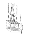
Classifications
-
- G—PHYSICS
- G02—OPTICS
- G02B—OPTICAL ELEMENTS, SYSTEMS OR APPARATUS
- G02B5/00—Optical elements other than lenses
- G02B5/30—Polarising elements
- G02B5/3083—Birefringent or phase retarding elements
-
- B—PERFORMING OPERATIONS; TRANSPORTING
- B29—WORKING OF PLASTICS; WORKING OF SUBSTANCES IN A PLASTIC STATE IN GENERAL
- B29D—PRODUCING PARTICULAR ARTICLES FROM PLASTICS OR FROM SUBSTANCES IN A PLASTIC STATE
- B29D11/00—Producing optical elements, e.g. lenses or prisms
- B29D11/00634—Production of filters
- B29D11/00644—Production of filters polarizing
-
- G—PHYSICS
- G02—OPTICS
- G02B—OPTICAL ELEMENTS, SYSTEMS OR APPARATUS
- G02B30/00—Optical systems or apparatus for producing three-dimensional [3D] effects, e.g. stereoscopic images
- G02B30/20—Optical systems or apparatus for producing three-dimensional [3D] effects, e.g. stereoscopic images by providing first and second parallax images to an observer's left and right eyes
- G02B30/26—Optical systems or apparatus for producing three-dimensional [3D] effects, e.g. stereoscopic images by providing first and second parallax images to an observer's left and right eyes of the autostereoscopic type
- G02B30/27—Optical systems or apparatus for producing three-dimensional [3D] effects, e.g. stereoscopic images by providing first and second parallax images to an observer's left and right eyes of the autostereoscopic type involving lenticular arrays
-
- G—PHYSICS
- G02—OPTICS
- G02B—OPTICAL ELEMENTS, SYSTEMS OR APPARATUS
- G02B5/00—Optical elements other than lenses
- G02B5/30—Polarising elements
- G02B5/3016—Polarising elements involving passive liquid crystal elements
-
- G—PHYSICS
- G02—OPTICS
- G02B—OPTICAL ELEMENTS, SYSTEMS OR APPARATUS
- G02B1/00—Optical elements characterised by the material of which they are made; Optical coatings for optical elements
- G02B1/10—Optical coatings produced by application to, or surface treatment of, optical elements
- G02B1/11—Anti-reflection coatings
-
- G—PHYSICS
- G02—OPTICS
- G02F—OPTICAL DEVICES OR ARRANGEMENTS FOR THE CONTROL OF LIGHT BY MODIFICATION OF THE OPTICAL PROPERTIES OF THE MEDIA OF THE ELEMENTS INVOLVED THEREIN; NON-LINEAR OPTICS; FREQUENCY-CHANGING OF LIGHT; OPTICAL LOGIC ELEMENTS; OPTICAL ANALOGUE/DIGITAL CONVERTERS
- G02F1/00—Devices or arrangements for the control of the intensity, colour, phase, polarisation or direction of light arriving from an independent light source, e.g. switching, gating or modulating; Non-linear optics
- G02F1/01—Devices or arrangements for the control of the intensity, colour, phase, polarisation or direction of light arriving from an independent light source, e.g. switching, gating or modulating; Non-linear optics for the control of the intensity, phase, polarisation or colour
- G02F1/13—Devices or arrangements for the control of the intensity, colour, phase, polarisation or direction of light arriving from an independent light source, e.g. switching, gating or modulating; Non-linear optics for the control of the intensity, phase, polarisation or colour based on liquid crystals, e.g. single liquid crystal display cells
- G02F1/133—Constructional arrangements; Operation of liquid crystal cells; Circuit arrangements
- G02F1/1333—Constructional arrangements; Manufacturing methods
- G02F1/1335—Structural association of cells with optical devices, e.g. polarisers or reflectors
- G02F1/13363—Birefringent elements, e.g. for optical compensation
- G02F1/133631—Birefringent elements, e.g. for optical compensation with a spatial distribution of the retardation value
-
- G—PHYSICS
- G02—OPTICS
- G02F—OPTICAL DEVICES OR ARRANGEMENTS FOR THE CONTROL OF LIGHT BY MODIFICATION OF THE OPTICAL PROPERTIES OF THE MEDIA OF THE ELEMENTS INVOLVED THEREIN; NON-LINEAR OPTICS; FREQUENCY-CHANGING OF LIGHT; OPTICAL LOGIC ELEMENTS; OPTICAL ANALOGUE/DIGITAL CONVERTERS
- G02F2202/00—Materials and properties
- G02F2202/36—Micro- or nanomaterials
Definitions
- the present invention relates to a retardation film comprising a substrate, an alignment layer, and a retardation layer containing a liquid crystal compound, a production method thereof, an image display device using the retardation film, and the like.
- FIG. 13 is a schematic diagram showing an example of a passive three-dimensional display using a liquid crystal display panel. In the example of FIG.
- pixels that are continuous in the vertical direction of the liquid crystal display panel are sequentially and alternately assigned to a right-eye pixel that displays a right-eye image and a left-eye pixel that displays a left-eye image. And driving with the image data for the left eye, thereby displaying the image for the right eye and the image for the left eye simultaneously.
- the screen of the liquid crystal display panel alternates between a region for displaying a right-eye image and a region for displaying a left-eye image, for example, by a strip-shaped region having a short side in a vertical direction and a long side in a horizontal direction. It is divided into.
- a pattern retardation film which is a retardation film provided with a patterned retardation layer, is arranged on the panel surface of the liquid crystal display panel, and light emitted by linearly polarized light from pixels for the right eye and the left eye is received. , Converted into circularly polarized light having different rotation directions for the right eye and the left eye. Therefore, in the pattern retardation film, two types of band-like regions in which the slow axis direction (direction in which the refractive index is maximum) are orthogonal to each other are sequentially formed corresponding to the setting of the region in the liquid crystal display panel.
- the passive method glasses equipped with corresponding polarizing filters are worn, and a right-eye image and a left-eye image are selectively provided to the viewer's right eye and left eye, respectively.
- the slow axis direction of the adjacent belt-like regions is usually a combination of + 45 ° and ⁇ 45 ° or 0 ° and + 90 ° with respect to the horizontal direction.
- the long side direction of the screen is shown as the horizontal direction in accordance with the name in the normal image display device.
- This passive method can also be applied to a liquid crystal display device with a slow response speed, and can also display three-dimensionally with a simple configuration using a pattern retardation film and circularly polarized glasses.
- Patent Document 1 discloses a method of forming a retardation layer by forming a photo-alignment layer with controlled orientation regulating force on a glass substrate and patterning the alignment of liquid crystals with this photo-alignment layer. It is disclosed. Further, in Patent Document 2, a photo-alignment layer is prepared by exposing the entire surface and then exposing using a mask, and aligning and curing the liquid crystal layer by the alignment regulating force of the photo-alignment layer. A method for producing a pattern retardation film is disclosed.
- so-called polarizing plate surface materials used for various display surfaces employ various light reflection prevention methods.
- One of the reflection prevention methods is a low refractive index thin film (so-called clear antireflection surface). Is formed on one side of the transparent substrate to form a clear antireflection layer with a low haze (cloudiness) of 0.5% or less, ensuring transparency and reducing reflectivity The method to do is adopted.
- various devices have been proposed in Patent Document 3 and the like.
- the antireflection by this clear surface material is achieved by creating a surface film made of a low refractive index material on the surface of the antireflection object, so that the reflected light reflected on the front side of this surface layer and the lower side surface of this surface layer The amount of the reflected light is reduced by interference with the reflected light reflected at, thereby preventing reflection.
- retardation film In an optical film such as a patterned retardation film (hereinafter referred to as “retardation film”), the difference in refractive index is generated based on a large difference in refractive index between the retardation layer and the alignment layer. There is a problem that unevenness occurs due to thin film interference and interference fringes occur. Accordingly, there is a demand for a retardation film that can effectively suppress interference fringes generated from the difference in refractive index between the retardation layer and the base material or alignment layer.
- Patent Document 4 a hard coat layer and a low refractive index layer are provided on the other surface of the transparent substrate against interference unevenness caused by refractive index difference and film thickness unevenness.
- an optical film that reduces the interference unevenness is disclosed.
- studies have been made to adjust the refractive index by adding an additive, but there is a problem that the orientation of the film is lowered. Therefore, there is a need for a retardation film that suppresses the generation of interference fringes while maintaining the orientation.
- antireflection is achieved by forming a clear antireflection layer on one side of the transparent base material, it can be placed on an image display panel for high quality. It is thought that the image of can be displayed.
- antiglare layer anti-glare: AG, which is another example of an antireflection layer.
- haze There is a problem that interference fringes due to thin film interference between the retardation layer and the transparent substrate are more easily seen than in the case of forming 1.0% or more). Accordingly, there is a need for a retardation film that can effectively suppress the occurrence of such interference fringes even when a clear antireflection layer is formed to prevent reflection.
- the present invention has been made in view of the situation as described above, and effectively suppresses interference fringes generated from the refractive index difference between the retardation layer and the alignment layer while maintaining the orientation in the retardation film.
- the purpose is to be able to.
- Another object of the present invention is to make it possible to effectively suppress interference fringes generated from a difference in refractive index between a retardation layer and a substrate or a pattern alignment layer.
- an optical film such as a pattern retardation film, it is intended to be able to effectively suppress the generation of interference fringes even when a clear antireflection layer is formed to prevent reflection. To do.
- the present inventor has included a high refractive index epoxy monomer in a predetermined ratio in the alignment layer, thereby maintaining the alignment property and preventing interference fringes.
- the inventors have found that generation can be effectively suppressed and completed the present invention.
- the inventor of the present invention includes an interference fringe even in the case where a clear antireflection layer is formed to prevent reflection by containing alkoxysilane, which is a low refractive index material, in a predetermined ratio in the retardation layer.
- the present invention was completed by finding that it can be effectively suppressed.
- the present inventor effectively prevents interference fringes even when a clear antireflection layer is formed to prevent reflection by incorporating predetermined fine particles having a low refractive index in the retardation layer.
- the inventors have found that it can be suppressed, and have completed the present invention. That is, the present invention provides the following.
- the present invention is a retardation film including a base material, an alignment layer containing a photo-alignment material, and a retardation layer containing a liquid crystal compound, and the alignment layer is 100 masses of the photo-alignment material. It is a retardation film containing an epoxy monomer having a refractive index of 1.60 or more in a proportion of 3.0 parts by mass or more and 8.0 parts by mass or less with respect to parts.
- the present invention is also the above-described (1) invention, wherein the epoxy monomer is a retardation film having a refractive index of 1.70 or more.
- the present invention has an in-plane variation of the optical axis defined by the standard deviation ( ⁇ ) when the optical axis is measured is less than 1.5. It is a certain retardation film.
- the present invention is the retardation film according to any one of the above-described inventions (1), (2), and (3), wherein the alignment layer has an alignment pattern.
- this invention is a polarizing plate provided with the phase difference film in any one of (1) to (4).
- this invention is an image display apparatus provided with the phase difference film in any one of (1) to (4).
- this invention is a 3D image display system provided with the image display apparatus as described in (6).
- this invention is a manufacturing method of retardation film containing the base material, the alignment layer containing a photo-alignment material, and the retardation layer containing a liquid crystal compound, Comprising: 100 mass parts of said photo-alignment materials
- An alignment layer composition containing an epoxy monomer having a refractive index of 1.60 or more in a proportion of 3.0 parts by mass or more and 8.0 parts by mass or less is used, and the alignment layer composition is applied onto the substrate. It is the manufacturing method of the retardation film which forms the said orientation layer by making it harden
- the present invention is a retardation film comprising a substrate, an alignment layer, and a retardation layer containing a liquid crystal compound, wherein the retardation layer is alkoxysilane with respect to 100 parts by mass of the liquid crystal compound.
- the present invention is the retardation film according to the above-described invention (9), wherein the alkoxysilane has a refractive index of 1.50 or less.
- the present invention has an in-plane variation of the optical axis defined by the standard deviation ( ⁇ ) when the optical axis is measured is less than 1.5. It is a certain retardation film.
- the orientation layer is a retardation film having an orientation pattern.
- this invention is a polarizing plate provided with the phase difference film in any one of (9) to (12).
- the present invention is an image display device including the retardation film according to any one of (9) to (12).
- this invention is a 3D image display system provided with the image display apparatus as described in (14).
- this invention is a manufacturing method of the retardation film containing a base material, an orientation layer, and the phase difference layer containing a liquid crystal compound, Comprising: 2 alkoxysilane is added with respect to 100 mass parts of said liquid crystal compounds.
- the present invention is also a retardation film in which an antireflection layer, a transparent substrate, an alignment layer, and a retardation layer including a polymerized liquid crystal are sequentially laminated, and the retardation layer gives a retardation to transmitted light.
- the antireflection layer is a clear antireflection layer having a haze value of 0.5% or less according to JISK7105
- the retardation layer is a retardation film containing fine particles having a refractive index lower than that of the polymerized liquid crystal.
- the present invention is the retardation film according to the invention of (17), wherein the fine particles have a refractive index of 1.3 or more and 1.7 or less.
- the average particle diameter of the fine particles is a retardation film larger than the thickness of the retardation layer.
- the fine particles are silica, and the content of the fine particles in the retardation layer is 0.01% by mass or more and 10% by mass. It is the following retardation film.
- the present invention is the retardation film according to any one of (17) to (20), wherein the retardation layer has a surface roughness Ra of 3 nm to 200 nm.
- the present invention is the retardation film according to any one of (17) to (21), wherein the transparent substrate is an acrylic resin and the thickness is 80 ⁇ m or less.
- the liquid crystal display device and the retardation layer of the pattern retardation film are close to each other, and the viewing angle of 3D display can be expanded.
- the present invention is also the retardation film according to any one of claims 17 to 22, wherein the alignment layer has an alignment pattern.
- this invention is a polarizing plate provided with the phase difference film in any one of (17) to (23).
- this invention is an image display apparatus provided with the phase difference film in any one of (17) to (23).
- this invention is a 3D image display system provided with the image display apparatus as described in (25).
- interference fringes caused by the retardation layer and the film interface are particularly easy to see.
- the refractive index of the phase difference layer By reducing the refractive index of the phase difference layer and bringing it closer to the refractive index of the transparent substrate, it is possible to provide an image display device and a 3D image display system that can suppress the generation of interference fringes.
- the present invention is also a retardation film in which an antireflection layer, a retardation layer containing a polymerized liquid crystal, an alignment layer, and a transparent substrate are sequentially laminated, and the retardation layer gives a retardation to transmitted light.
- the antireflection layer is a clear antireflection layer having a haze value of 0.5% or less according to JISK7105
- the retardation layer is a retardation film containing fine particles having a refractive index lower than that of the polymerized liquid crystal.
- the present invention is a retardation film in which an antireflection layer, a transparent substrate, an alignment layer, and a retardation layer containing a polymerized liquid crystal are sequentially laminated, and the retardation film gives a retardation to transmitted light.
- the antireflection layer is a clear antireflection layer having a haze value of 0.5% or less according to JISK7105,
- the refractive index of the transparent substrate is n1
- the refractive index of the alignment layer is n2
- the refractive index of the retardation layer is n3, n1 ⁇ n2 ⁇ n3,
- the occurrence of interference fringes can be suppressed by setting the refractive index of the alignment layer to a substantially intermediate value between the refractive index of the transparent substrate and the refractive index of the retardation layer.
- the present invention is the retardation film according to the invention of (28), wherein the transparent substrate is an acrylic resin having a thickness of 80 ⁇ m or less.
- the liquid crystal display device and the retardation layer of the pattern retardation film are brought closer to each other, and the viewing angle of 3D display can be expanded.
- the present invention is the retardation film according to the invention (28) or (29), wherein the refractive index n2 of the alignment layer is 1.53 or more and 1.56 or less.
- the generation of interference fringes can be particularly effectively suppressed when the transparent substrate is an acrylic resin and the refractive index is around 1.50.
- the present invention is the retardation film according to any one of (28) to (30), wherein the alignment layer is composed of a light dimerization type polymer material.
- the alignment layer includes a photodimerization-type polymer material and an additive for adjusting a refractive index. It is a film.
- the refractive index of the light dimerization type polymer material in addition to the refractive index of the light dimerization type polymer material, it can be adjusted to a desired refractive index by an additive.
- the present invention is the retardation film according to any one of (28) to (32), wherein the alignment layer has an alignment pattern.
- the present invention is a polarizing plate comprising the retardation film according to any one of (28) to (33).
- the present invention is an image display device comprising the retardation film according to any one of (28) to (33).
- the occurrence of interference fringes can be suppressed by adjusting the refractive index of the alignment layer so as to have a substantially intermediate value between the refractive index of the transparent substrate and the refractive index of the retardation layer.
- the present invention is a 3D image display system including the image display device according to (35).
- the present invention is a retardation film in which an antireflection layer, a retardation layer containing a polymerized liquid crystal, an alignment layer, and a transparent substrate are sequentially laminated, and the retardation layer gives a retardation to transmitted light.
- the antireflection layer is a clear antireflection layer having a haze value of 0.5% or less according to JISK7105,
- the refractive index of the transparent substrate is n1
- the refractive index of the alignment layer is n2
- the refractive index of the retardation layer is n3, n1 ⁇ n2 ⁇ n3,
- the occurrence of interference fringes can be suppressed by setting the refractive index of the alignment layer to a substantially intermediate value between the refractive index of the transparent substrate and the refractive index of the retardation layer.
- the present invention by containing an epoxy monomer in a predetermined ratio in the alignment layer, it is possible to effectively suppress interference fringes generated from the difference in refractive index of the film while maintaining good alignment. Moreover, according to this invention, the interference fringe which arises from the refractive index difference of a film
- membrane can be suppressed by making a retardation layer contain alkoxysilane by a predetermined ratio. Moreover, even when the additive is added to the retardation layer in this way, interference fringes can be effectively suppressed while maintaining good orientation. Further, according to the present invention, even when a clear antireflection layer is formed to prevent reflection, the generation of interference fringes can be suppressed.
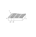
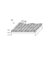
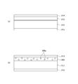
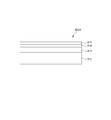
- FIG. 1 It is the schematic which shows an example of the pattern phase difference film which concerns on 4th Embodiment. It is an expanded sectional view of FIG. It is an expanded sectional view which shows the pattern phase difference film by another example. It is a figure where it uses for description of the three-dimensional image display by a passive system.
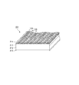
- FIG. 1 is a diagram showing a pattern retardation film applied to the image display device according to the first embodiment of the present invention.
- the pixels of the liquid crystal display panel that are continuous in the vertical direction sequentially and alternately display the right-eye image.
- the pixels are assigned to the left-eye pixels for displaying the left-eye image and the left-eye image, and are driven by the right-eye and left-eye image data, respectively.
- the image display device alternately divides the display screen into a band-like region for displaying an image for the right eye and a band-like region for displaying an image for the left eye, so that the image for the right eye and the image for the left eye are divided. Display at the same time.
- a pattern phase difference film 1 is disposed on the panel surface (viewer side surface) of the liquid crystal display panel, and the pattern phase difference film 1 corresponds to light emitted from right-eye and left-eye pixels, respectively. To give the phase difference.
- this image display apparatus displays a desired three-dimensional image by a passive method.
- video content related to 3D image display is provided from a desired source source and displayed on the image display device, and the corresponding circular polarized glasses are attached to view the 3D video content.
- the image display device is premised on the application of a liquid crystal display panel, the polarizing plate is bonded to a linear polarizing plate provided on the exit surface side of the liquid crystal display panel so as to include a pattern retardation film. You may make it supply.
- the pattern retardation film 1 is a retardation film provided with a patterned retardation layer.
- the pattern retardation film 1 is characterized in that the pattern alignment layer 12 contains a high refractive index epoxy monomer at a predetermined ratio.
- the base material 11 is a transparent film material, has a function of supporting the pattern alignment layer 12, and is formed in a long shape.
- the substrate 11 preferably has a small phase difference, and an in-plane retardation (in-plane retardation value, hereinafter also referred to as “Re value”) is preferably in the range of 0 nm or more and 10 nm or less, and 0 nm or more. More preferably, it is in the range of 5 nm or less, and further preferably in the range of 0 nm or more and 3 nm or less. If the Re value exceeds 10 nm, the display quality of a flat panel display using a pattern alignment layer may be deteriorated, which is not preferable.
- in-plane retardation value in-plane retardation value
- the Re value is an index indicating the degree of birefringence in the in-plane direction of the refractive index anisotropic body.
- the refractive index in the slow axis direction having the largest refractive index in the in-plane direction is Nx
- the slow axis direction is in the slow axis direction.
- Re [nm] (Nx ⁇ Ny) ⁇ d [nm] It is a value represented by.
- the Re value can be measured by, for example, a parallel Nicol rotation method using a phase difference measuring device KOBRA-WR (manufactured by Oji Scientific Instruments). Further, in this specification, unless otherwise specified, the Re value means a value at a wavelength of 589 nm.
- the transmittance of the substrate 11 in the visible light region is preferably 80% or more, and more preferably 90% or more.
- the transmittance of the transparent film substrate can be measured according to JIS K7361-1 (Plastic—Testing method of total light transmittance of transparent material).
- flexible materials include acrylic polymers, cellulose derivatives, norbornene polymers, cycloolefin polymers, polymethyl methacrylate, polyvinyl alcohol, polyimide, polyarylate, polyethylene terephthalate, polysulfone, polyethersulfone, amorphous polyolefin, polystyrene, Examples include epoxy resins, polycarbonates, polyesters, and the like.
- the cellulose derivative is excellent in optical isotropy and can produce a pattern alignment layer having excellent optical properties.
- the cellulose derivative is not particularly limited, but it is preferable to use a cellulose ester, and more preferable to use cellulose acylates because they are widely used industrially and are easily available.
- lower fatty acid esters having 2 to 4 carbon atoms are preferable.
- the lower fatty acid ester may include only a single lower fatty acid ester such as cellulose acetate, and may include a plurality of fatty acid esters such as cellulose acetate butyrate and cellulose acetate propionate. Good.
- cellulose acetate can be particularly preferably used.
- TAC having an average acetylation degree of 57.5% or more and 62.5% or less (substitution degree: 2.6 or more and 3.0 or less) is most preferably used.
- the degree of acetylation means the amount of bound acetic acid per unit mass of cellulose.
- the degree of acetylation can be determined by measuring and calculating the degree of acetylation in ASTM: D-817-91 (Testing method for cellulose acetate and the like).
- the acetylation degree of TAC can be calculated
- An acrylic polymer (acrylic base material) such as PMMA has a refractive index of about 1.40 to 1.60, has no refractive index difference in the thickness direction of the base material, and has a dimensional shrinkage ratio against humidity. Low dependency. Therefore, for example, the film thickness can be reduced as compared with TAC, which can contribute to the expansion of the viewing angle of the 3D panel.
- the thickness of the substrate 11 is not particularly limited as long as it is within a range in which the necessary self-supporting property can be imparted to the retardation film, depending on the use of the retardation film produced using the pattern alignment layer. Usually, it is preferably in the range of 25 ⁇ m or more and 125 ⁇ m or less, more preferably in the range of 40 ⁇ m or more and 100 ⁇ m or less, and further preferably in the range of 40 ⁇ m or more and 80 ⁇ m or less. If the thickness is less than 25 ⁇ m, the necessary self-supporting property may not be imparted to the retardation film, which is not preferable. On the other hand, when the thickness exceeds 125 ⁇ m, when the retardation film is long, processing waste increases when the long retardation film is cut into a single-phase retardation film. Or wear of the cutting blade may be accelerated.
- the substrate 11 is not limited to a single layer configuration, and may have a configuration in which a plurality of layers are stacked.
- the layer of the same composition may be laminated
- FIG. 2 is a schematic view of the pattern alignment layer 2.
- the pattern alignment layer 2 is made of a cured product obtained by coating (coating) a composition for pattern alignment layer (alignment layer composition) on the substrate 11 and curing the pattern alignment layer 2.
- An alignment layer 12 is formed.
- the pattern alignment layer 2 has two types of alignment patterns (first alignment region 12A and second alignment region 12B) alternately.
- the alignment pattern in the pattern alignment layer 2 can be formed by a photo-alignment method in which alignment is performed by light irradiation using a photo-alignment material that exhibits photo-alignment properties by irradiation with polarized light.
- an ultraviolet curable resin is apply
- the orientation pattern is transcribe
- the pattern alignment layer 12 When forming the pattern alignment layer 12 by a photo-alignment method, the pattern alignment layer 12 contains a composition for a pattern alignment layer (alignment layer composition), and this alignment layer composition exhibits photo-alignment properties by irradiation with polarized light.
- a photo-alignment material A photo-alignment material.
- the photo-alignment material refers to a material that can exhibit an alignment regulating force by irradiation with polarized ultraviolet rays.
- the alignment regulating force means that when an alignment layer containing a photo-alignment material is formed and a layer (retardation layer 13) made of a polymerizable liquid crystal compound (also referred to as “rod-like compound”) is formed on the alignment layer, It refers to the function of aligning liquid crystal compounds in a predetermined direction.
- the photo-alignment material is not particularly limited as long as it exerts alignment regulating power by irradiating polarized light.
- Such photo-alignment materials include a photoisomerization material that reversibly changes the alignment regulating force by changing only the molecular shape by cis-trans change, and a photoreaction material that changes the molecule itself by irradiating polarized light. Can be broadly classified.
- any of the above-mentioned photoisomerization material and photoreaction material can be suitably used, but it is more preferable to use a photoreaction material.
- the photoreactive material is a material that reacts with polarized light and reacts with molecules to develop an orientation regulating force. Therefore, it is possible to irreversibly develop an orientation regulating force, and the stability over time of the orientation regulating force is achieved. Excellent in.
- photoreactive materials include photodimerization-type materials that exhibit orientation-regulating power due to photo-dimerization reactions, photo-decomposable materials that exhibit orientation-controlling power due to photodecomposition reactions, and photo-bonding reactions that occur. It can be divided into a photo-coupled material that exhibits an orientation regulating force and a photodecomposition-coupled material that exhibits an orientation regulating force due to the occurrence of a photodecomposition reaction and a photo-coupling reaction.
- any of the photoreactive materials described above can be suitably used, but it is more preferable to use a photodimerization type material.
- the photodimerization type material is not particularly limited as long as it is a material capable of expressing the alignment regulating force by causing the photodimerization reaction, but the wavelength of light causing the photodimerization reaction is 280 nm or more from the point that the alignment regulating force is good. Preferably, it is in the range of 280 nm or more and 400 nm or less, and more preferably in the range of 300 nm or more and 380 nm or less.
- Examples of such a photodimerization type material include polymers having cinnamate, coumarin, benzylidenephthalimidine, benzylideneacetophenone, diphenylacetylene, stilbazole, uracil, quinolinone, maleimide, or cinnamilidene acetic acid derivatives.
- a polymer having one or both of cinnamate and coumarin is preferably used from the viewpoint of good alignment regulating power.
- Specific examples of such a photodimerization type material include compounds described in, for example, JP-A-9-118717, JP-T-10-506420, JP-T2003-505561, and WO2010 / 150748. Can be mentioned.
- the photo-alignment material used in this Embodiment may be only one type, and may use 2 or more types.
- the refractive index of the alignment layer which usually constitutes a general pattern alignment layer is about 1.54.
- the refractive index of the polymerizable liquid crystal is about 1.55 to 1.75, which is higher than the refractive index of the pattern alignment layer. For this reason, unevenness due to thin film interference between the retardation layer and the substrate may occur due to a difference in refractive index between the pattern alignment layer and the retardation layer, and interference fringes may occur.
- the pattern alignment layer 12 does not contribute to the alignment of the liquid crystal compound even if it is exposed to a high refractive index material. It is characterized by containing a predetermined percentage of epoxy monomer.
- Such a pattern alignment layer 12 is obtained by coating the alignment layer composition with a photo-alignment material together with an epoxy monomer at a predetermined ratio and coating the substrate 11 using the alignment layer composition. be able to.
- the refractive index of the pattern alignment layer 12 is effectively increased by containing the epoxy monomer having a high refractive index in a predetermined ratio in the pattern alignment layer 12 as described above.
- Generation of interference fringes due to a difference in refractive index between the pattern alignment layer 12 and the retardation layer 13 can be suppressed.
- interference fringes can be effectively suppressed without narrowing the range of selection of materials constituting the pattern alignment layer 12 and the retardation layer 13.
- the in-plane variation of the optical axis in the micro area when measured with the optical axis is less than 1.5 in standard deviation ( ⁇ ).
- ⁇ standard deviation
- the variation in the optical axis can be defined by the standard deviation ( ⁇ ) (unit: °) of the optical axis.
- the bifunctional type epoxy which has a fluorene skeleton which is a compound (compound shown by the formula (1) described in the said gazette) of Unexamined-Japanese-Patent No. 2012-102228 Mention may be made of monomers.
- this high refractive index epoxy monomer has a refractive index of 1.60 or more.
- the refractive index of the epoxy monomer is more preferably 1.70 or more. If the refractive index is less than 1.60, it is difficult to adjust the refractive index and the generation of interference fringes may not be sufficiently suppressed.
- the content of the high refractive index epoxy monomer in the pattern alignment layer 12 is also important, and is 3.0 parts by mass or more and 8.0 parts by mass or less with respect to 100 parts by mass of the photo-alignment material included in the pattern alignment layer 12. Range.
- the content is preferably in the range of 3.0 parts by mass or more and 7.0 parts by mass or less, more preferably about 5.0 parts by mass with respect to 100 parts by mass of the photo-alignment material. If the content is less than 3.0 parts by mass, the refractive index of the pattern alignment layer 12 cannot be sufficiently increased, and the generation of interference fringes cannot be effectively suppressed. On the other hand, if the content exceeds 8.0 parts by mass, not only the interference fringes cannot be effectively suppressed, but also the orientation may be lowered, which is not preferable.
- the solvent used in the alignment layer composition is not particularly limited as long as it can dissolve the photo-alignment material and the above-described high refractive index epoxy monomer at a desired concentration.
- hydrocarbons such as benzene and hexane Solvents, ketone solvents such as methyl ethyl ketone, methyl isobutyl ketone, cyclohexanone (CHN), ether solvents such as tetrahydrofuran, 1,2-dimethoxyethane, propylene glycol monoethyl ether (PGME), alkyl halides such as chloroform and dichloromethane Solvents, ester solvents such as methyl acetate, ethyl acetate, butyl acetate, propylene glycol monomethyl ether acetate (PGMEA), amide solvents such as N, N-dimethylformamide, sulfoxide solvents such as dimethyl sulfoxide, cyclohexane Sol
- the amount of the solvent is preferably 600 parts by mass or more and 3900 parts by mass or less with respect to 100 parts by mass of the photo-alignment material, for example. If it is less than 600 parts by mass, the photo-alignment material may not be dissolved uniformly, which is not preferable. When the amount of the solvent exceeds 3900 parts by mass, a part of the solvent remains, and the solvent remaining when the alignment layer composition is applied onto the base material 11 is impregnated into the base material 11 so that the photo-alignment property is obtained. And the adhesion to the base material 11 are undesirably lowered.
- the retardation layer 13 contains a polymerizable liquid crystal composition.
- This polymerizable liquid crystal composition contains a liquid crystal compound (rod-like compound) exhibiting liquid crystallinity and having a polymerizable functional group in the molecule.
- the liquid crystal compound has a refractive index anisotropy, and has a function of imparting a desired retardation by regularly arranging along the alignment pattern.
- the liquid crystal compound include materials exhibiting a liquid crystal phase such as a nematic phase and a smectic phase, but the nematic phase is easier to arrange regularly than liquid crystal compounds exhibiting other liquid crystal phases. It is more preferable to use the liquid crystal compound shown.
- the liquid crystal compound exhibiting a nematic phase it is preferable to use a material having spacers at both ends of the mesogen. Since the liquid crystal compound having spacers at both ends of the mesogen is excellent in flexibility, the pattern retardation film 1 can be made excellent in transparency by using such a liquid crystal compound.
- the liquid crystal compound has a polymerizable functional group in the molecule as described above. By having a polymerizable functional group, it is possible to polymerize and fix the liquid crystal compound, so that the alignment stability is excellent and the phase change is less likely to occur over time.
- the liquid crystal compound more preferably has a polymerizable functional group capable of three-dimensional crosslinking in the molecule. By having a polymerizable functional group capable of three-dimensional crosslinking, the sequence stability can be further enhanced. Note that “three-dimensional crosslinking” means that liquid crystal molecules are polymerized three-dimensionally to form a network structure.
- polymerizable functional group examples include polymerizable functional groups that are polymerized by the action of ionizing radiation such as ultraviolet rays and electron beams, or heat.
- polymerizable functional groups include radically polymerizable functional groups or cationic polymerizable functional groups.
- radically polymerizable functional groups include functional groups having at least one addition-polymerizable ethylenically unsaturated double bond, and specific examples include vinyl groups and acrylates with or without substituents.
- Group (a generic name including an acryloyl group, a methacryloyl group, an acryloyloxy group, and a methacryloyloxy group).
- examples of the polymerizable functional group include an isocyanate group and an unsaturated triple bond.
- a functional group having an ethylenically unsaturated double bond is preferably used from the viewpoint of the process.
- the liquid crystal compound has a polymerizable functional group at the terminal.
- a liquid crystal compound for example, they can be polymerized three-dimensionally to form a network structure, so that they have column stability and excellent optical properties.
- Pattern retardation film 1 can be formed.
- the amount of the liquid crystal compound is not particularly limited as long as the viscosity of the retardation layer forming coating liquid (liquid crystal composition) can be adjusted to a desired value according to the coating method applied on the pattern alignment layer 12.
- the amount in the liquid crystal composition is preferably in the range of 5 to 40 parts by weight, and more preferably in the range of 10 to 30 parts by weight. If the amount is less than 5 parts by mass, the amount of liquid crystal compound is too small, and therefore, there is a possibility that the incident light to the retardation layer 13 may not be properly aligned. On the other hand, when the amount exceeds 30 parts by mass, the viscosity of the retardation layer forming coating solution becomes too high, which is not preferable because workability is inferior.
- liquid crystal compound having one or more polymerizable functional groups at both ends and a liquid crystal compound having one or more polymerizable functional groups at one end are mixed and used as a liquid crystal compound, Polymerization density (crosslinking density) and optical characteristics can be arbitrarily adjusted. From the viewpoint of ensuring reliability, it is preferable to use a liquid crystal compound having one or more polymerizable functional groups at both ends, but from the viewpoint of liquid crystal alignment, a liquid crystal compound having one polymerizable functional group at both ends is used. It is preferable to use it.
- solvent The liquid crystal compound described above is usually dissolved in a solvent.
- the solvent is not particularly limited as long as the liquid crystal compound can be uniformly dispersed.
- hydrocarbon solvents such as benzene and hexane
- ketone solvents such as methyl ethyl ketone, methyl isobutyl ketone, and cyclohexanone (CHN).
- Ether solvents such as tetrahydrofuran, 1,2-dimethoxyethane, propylene glycol monoethyl ether (PGME), alkyl halide solvents such as chloroform and dichloromethane, methyl acetate, ethyl acetate, butyl acetate, propylene glycol monomethyl ether acetate ( Ester solvents such as PGMEA), amide solvents such as N, N-dimethylformamide, sulfoxide solvents such as dimethyl sulfoxide, anone solvents such as cyclohexane, methanol, ethanol, isopropyl Alcohol can be exemplified (hereinafter referred to as "IPA”.) Alcoholic solvents such as but not limited thereto. Moreover, one type of solvent may be sufficient and the mixed solvent of two or more types of solvents may be sufficient.
- the amount of the solvent is preferably 66 parts by mass or more and 900 parts by mass or less with respect to 100 parts by mass of the liquid crystal compound. If the amount of the solvent is less than 66 parts by mass, the liquid crystal compound may not be dissolved uniformly, which is not preferable. On the other hand, when the amount exceeds 900 parts by mass, a part of the solvent remains, which may reduce reliability and may not be uniformly applied.
- the liquid crystal composition may contain other compounds as necessary.
- Other compounds are not particularly limited as long as they do not impair the alignment order of the liquid crystal compounds described above. Examples include polymerization initiators, polymerization inhibitors, plasticizers, surfactants, and silane coupling agents. Can be mentioned. For example, when a silicone-based high molecular weight leveling agent is added as a leveling agent, the addition amount is about 0.1% or more and less than 1%.
- the thickness of the retardation layer 13 is not particularly limited, but is preferably 500 nm or more and 2000 nm or less in order to obtain appropriate alignment performance.
- the manufacturing method of the pattern phase difference film 1 is demonstrated.
- the pattern retardation film 1 may be formed by the shaping UV method.
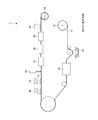
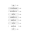
- FIG. 3 is a diagram schematically showing the flow of the manufacturing process of the pattern retardation film 1.
- a substrate 11 is provided from a long film wound on a roll 31, and a pattern alignment layer composition (alignment layer composition) 32 is applied on the substrate 11.
- a pattern alignment layer composition (alignment layer composition) 32 is applied on the substrate 11.
- a pattern alignment layer forming layer forming process is performed in which the alignment layer composition is thermally cured by a dryer 33 to form a thin film pattern alignment layer forming layer 12 ′.
- (C) the ultraviolet irradiation process of irradiating the pattern alignment layer forming layer 12 ′ with ultraviolet rays from the ultraviolet irradiation devices 34 and 35 is performed.
- the pattern alignment layer 12 is formed by the processes (A) to (C).
- a retardation layer forming coating solution 13 ′ is applied from a retardation layer forming coating solution supply device 36 containing a polymerizable liquid crystal composition for forming a retardation layer.
- a coating solution for forming a retardation layer for forming a layer forming layer is applied.
- a leveling process is performed using the leveling device 37 to make the thickness of the retardation layer forming layer uniform.
- the pattern alignment layer 12 mentioned above has by heating the liquid crystal compound contained in the coating film of the coating liquid 13 ′ for retardation layer formation using the dryer 38 to the liquid crystal phase formation temperature or higher.
- Alignment treatment is performed to align the liquid crystal compounds along different alignment directions of the first alignment region 12A corresponding to the right-eye region and the second alignment region 12B corresponding to the left-eye region.
- the retardation layer forming layer becomes the retardation layer 13.
- the base material 11 is provided from the long film wound up by the roll 31, and the orientation layer composition coating process which coats the composition 32 for pattern orientation layers on this base material 11 is performed.
- the method using a general conveyance means can be used. Specific examples include a method using an unwinder that feeds a roll-shaped long film, a winder that winds the long film, and a method that uses a belt conveyor, a transport roll, and the like. Moreover, the method of using the floating type conveyance stand which conveys in the state which floated the film for elongate orientation layer formation by performing discharge and suction
- the color of the conveying means is preferably a color that does not reflect the ultraviolet light that has passed through the long film when it is disposed at a site where the long film is irradiated with ultraviolet light.
- black is preferable. Examples of such a black method include a method of chromium treatment of the surface.
- the shape of the roll 31 is not particularly limited as long as it can stably convey a long film, but when it is arranged at a site where the long film is irradiated with ultraviolet rays, It is preferable that the distance between the surface of the long film and the ultraviolet irradiation device can be kept constant, and it is usually preferable to have a perfect circle shape.
- the base material 11 is pulled out from the roll 31 and sequentially subjected to anti-glare treatment (AG treatment), anti-reflection treatment (AR treatment), etc.
- An antireflection layer can be formed.
- the coating method includes die coating method, gravure coating method, reverse coating method, knife coating method, dip coating method, spray coating method, air knife coating method, spin coating method, roll.
- a coating method, a printing method, a dipping method, a curtain coating method, a casting method, a bar coating method, an extrusion coating method, an E-type coating method, and the like can be used.
- the thickness of the pattern alignment layer forming layer 12 ′ is not particularly limited as long as the desired planarity can be achieved, but is preferably in the range of 0.1 ⁇ m or more and 10 ⁇ m or less, More preferably, it is in the range of 0.1 ⁇ m or more and 5 ⁇ m or less, and further preferably in the range of 0.1 ⁇ m or more and 3 ⁇ m or less.
- the alignment layer composition 32 an epoxy monomer having a refractive index of 1.60 or more is combined with the photo-alignment material by 3.0 parts by mass or more and 8 parts by mass with respect to 100 parts by mass of the photo-alignment material.
- the composition contained in the range of 0.0 part by mass or less is used.
- the alignment layer composition 32 applied to the substrate 11 using the dryer 33 is thermally cured.
- the base material 11 coated with the alignment layer composition 32 is guided to a dryer 33, and the alignment layer composition 32 is thermally cured and then sent to the next step in a semi-dry state.
- the curing temperature of the alignment layer composition 32 is preferably 100 ° C. or higher and 130 ° C. or lower. When the curing temperature is less than 100 ° C., the alignment layer composition 32 cannot be uniformly cured by heat, and the thin film may become non-uniform. On the other hand, if the curing temperature exceeds 130 ° C., the substrate 11 and the thin film may shrink, which is not preferable.
- the curing time of the alignment layer composition 32 is preferably 1 minute or more and less than 10 minutes. If the curing time is less than 1 minute, it cannot be thermally cured and the thin film may become non-uniform, which is not preferable. On the other hand, if the curing time is 10 minutes or longer, there is a possibility that repelling or defects may occur, and the base material 11 or the thin film may shrink.
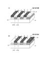
- an ultraviolet irradiation process for irradiating the pattern alignment layer forming layer 12 'with ultraviolet rays is performed.
- this ultraviolet irradiation process first, as shown in FIG. 4A, the first alignment preparation region 12′A corresponding to the right eye region is not shielded, and the second alignment preparation corresponding to the left eye region is performed.
- the pattern alignment layer forming layer 12 ′ with ultraviolet rays polarized ultraviolet rays
- the first alignment preparation region 12′A is first irradiated with polarized ultraviolet light, and then the second alignment preparation region 12′B is irradiated with polarized ultraviolet light.
- the second alignment preparation region 12′B may be irradiated with polarized ultraviolet light
- the first alignment preparation region 12′A may be irradiated with polarized ultraviolet light.
- the masks 21 and 22 are used for both the first irradiation and the second irradiation, but the mask 21 is used only for the first irradiation and the mask 22 is not used for the second irradiation. May be performed.
- the mask pattern that is, the pattern irradiation pattern, stabilizes the first alignment region 12A (see FIG. 2) corresponding to the right eye region and the second alignment region 12B (see FIG. 2) corresponding to the left eye region.
- it can be a pattern shape such as a band pattern, a mosaic pattern, or a staggered pattern.
- a belt-like pattern is preferable, and in particular, a belt-like pattern parallel to each other in the longitudinal direction of the long film, that is, pattern irradiation is polarized into a belt-like pattern parallel to each other in the longitudinal direction of the long film. It is preferable to irradiate with ultraviolet rays.
- the pattern width of the mask that is, the irradiation width and irradiation interval (non-irradiation width) of polarized ultraviolet rays may be the same or different, but the width of the region corresponding to the right eye region
- the width of the region corresponding to the region for the left eye is preferably the same.
- the pattern in which the region corresponding to the region for the right eye and the region corresponding to the region for the left eye are formed and the stripe pattern of the color filter have a correspondence relationship. It is preferable to irradiate with such a width.
- the pattern width is preferably in the range of 50 ⁇ m or more and 1000 ⁇ m or less, and more preferably in the range of 100 ⁇ m or more and 800 ⁇ m or less.
- the pattern width here refers to the pattern width of the pattern orientation layer 12 when the base material 11 is in a stably contracted state.
- the material constituting the mask is not particularly limited as long as a desired opening can be formed, and examples thereof include metals and quartz that are hardly deteriorated by ultraviolet rays.
- a metal substrate such as SUS that has been patterned by etching, laser processing, or electroforming, and further subjected to surface treatment such as nickel plating as necessary can be used.
- a light shielding film made of emulsion (silver salt) or chromium can be provided on a substrate made of soda lime glass or quartz.
- Cr is patterned on synthetic quartz. Excellent in dimensional stability and ultraviolet transmittance with respect to temperature change, humidity change, etc., and the pattern alignment layer forming layer 12 'made of a cured product of the pattern alignment layer composition can be irradiated with ultraviolet rays with high accuracy, resulting in a highly accurate pattern.
- the alignment layer 12 can be formed.
- the thickness of the synthetic quartz mask is not particularly limited as long as it can form a pattern with high dimensional accuracy, but is preferably in the range of 1 mm to 20 mm, and preferably in the range of 5 mm to 18 mm. More preferably, it is in the range of 9 mm or more and 16 mm or less. When the thickness is within the above-described range, it can be prevented from bending and can have high dimensional accuracy. Moreover, it is preferable also from the point of the handleability as a photomask.
- the polarization direction of the polarized ultraviolet light is not particularly limited as long as the polarization direction with respect to the region corresponding to the region for the right eye and the polarization direction with respect to the region corresponding to the region for the left eye are different. It is preferable that the difference is 90 °.
- the direction different by 90 ° means that when a display device capable of three-dimensional display is formed using the phase difference film obtained by cutting out the long pattern phase difference film 1, three-dimensional display can be performed with high accuracy. If it is, it will not specifically limit. Usually, it is preferably within a range of 90 ° ⁇ 3 °, more preferably within a range of about 90 ° ⁇ 2 °, and further preferably within a range of about 90 ° ⁇ 1 °.
- the polarized ultraviolet light may be collected or may not be collected. However, when the pattern irradiation is performed on the long film on the transport roll, that is, the polarized ultraviolet light. When there is a difference in the distance from the light source of polarized ultraviolet light within the region irradiated with, the light is preferably condensed with respect to the transport direction. Thereby, the influence by the distance from a light source can be reduced, and an orientation area
- the wavelength of the polarized ultraviolet light is appropriately set according to the photo-alignment material and the like, and can be a wavelength used when expressing the alignment regulating force in a general photo-alignment material.
- Irradiation light having a wavelength of 210 nm to 380 nm, preferably 230 nm to 380 nm, and more preferably 250 nm to 380 nm is preferably used.
- the method for generating polarized ultraviolet rays is not particularly limited as long as it is a method capable of stably irradiating polarized ultraviolet rays, but a method of irradiating ultraviolet rays through a polarizer that can pass only polarized light in a certain direction is used. it can.
- a polarizer one that is generally used for generation of polarized light can be used.
- a wire grid polarizer having a slit-shaped opening or a plurality of quartz plates are laminated. Examples thereof include a method of performing polarization separation using a Brewster angle, and a method of using a method of performing polarization separation using a Brewster angle of vapor-deposited multilayer films having different refractive indexes.
- the irradiation amount (integrated light amount) of polarized ultraviolet rays is not particularly limited as long as an alignment region having a desired alignment regulating force can be formed.
- the wavelength is 310 nm
- 5 mJ / cm. preferably in the range of 2 or more 500 mJ / cm 2 or less, more preferably in the range of 7 mJ / cm 2 or more 300 mJ / cm 2 or less, 10 mJ / cm 2 or more 100 mJ / cm 2 within the range More preferably it is.
- an alignment region having a sufficient alignment regulating force can be formed.
- the temperature of the thin film is preferably 15 ° C. or higher and 90 ° C. or lower, and more preferably 15 ° C. or higher and 60 ° C. or lower.
- Examples of the temperature control method include a method using a temperature control device such as a general heating / cooling device.
- the retardation layer forming coating solution is applied from the supply device 36 of the retardation layer forming coating solution onto the formed pattern alignment layer 12.
- the coating method is not particularly limited as long as it is a method capable of stably coating a coating film made of a retardation layer forming coating liquid on the pattern alignment layer 12, and (A) alignment layer composition coating is not limited. The same thing as what was demonstrated by the construction process can be illustrated.
- the retardation layer 13 exhibits a retardation by containing a liquid crystal compound, and the degree of the retardation depends on the type of the liquid crystal compound and the thickness of the retardation layer 13. To be determined. Accordingly, the thickness of the phase difference layer forming layer is not particularly limited as long as it is within a range in which a predetermined retardation can be achieved, and is appropriately determined according to the use of the pattern retardation film 1 and the like. Can do.
- the leveling device 37 is used to perform a leveling process for making the thickness of the retardation layer forming layer uniform.
- the retardation layer forming layer is formed by coating the retardation layer forming coating liquid so that the in-plane retardation of the retardation layer 13 formed thereafter has a thickness within a range corresponding to ⁇ / 4 minutes. It is preferable to apply.
- the linearly polarized light passing through the first retardation region 13A and the second retardation region 13B can be made into circularly polarized light that is orthogonal to each other, and as a result, a three-dimensional image can be displayed with higher accuracy. it can.
- the specific distance is appropriately determined according to the type of the liquid crystal compound.
- the distance is in the range of 0.5 ⁇ m to 2 ⁇ m, but is not limited thereto.
- the liquid crystal compound contained in the coating film of the retardation layer forming coating liquid is changed along the different alignment directions of the first alignment region 12A and the second alignment region 12B included in the pattern alignment layer 12.
- the method for aligning the liquid crystal compound is not particularly limited as long as it can be aligned in a desired direction.
- the liquid crystal compound is heated to a temperature higher than the liquid crystal phase formation temperature by using a dryer 38. Methods and the like.
- the pattern of the retardation layer 13 formed by this alignment treatment is the same as the pattern of the pattern alignment layer 12, and on the first alignment region 12A corresponding to the right eye region, the first corresponding to the right eye region is formed.
- a phase difference region 13A is formed, and a second phase difference region 13B corresponding to the left eye region is formed on the second alignment region 12B corresponding to the left eye region.
- the method for polymerizing the polymerizable liquid crystal compound may be arbitrarily determined according to the type of the polymerizable functional group possessed by the polymerizable liquid crystal compound, but is a method in which an appropriate amount of a polymerization initiator is added and cured by irradiation with actinic radiation. Is preferred.
- the actinic radiation is not particularly limited as long as it is a radiation capable of polymerizing a polymerizable liquid crystal compound, but usually, ultraviolet light or visible light can be used from the viewpoint of the ease of the apparatus.
- the liquid crystal compounds are polymerized with each other to be in a network structure, have a column stability, and have excellent optical characteristics. 13 can be formed.
- Example 1-1 As a base material, an acrylic film 40 ⁇ m (refractive index: 1.48) whose surface is antiglare-treated is used, and on the back side thereof, a polyvinyl cinnamate (PVCi) group is formed so that the film thickness after curing is 200 nm.
- PVCi polyvinyl cinnamate
- a photo-alignment material having a refractive index of 3.0 and 3.0 parts by mass of an epoxy monomer having a refractive index of 1.70 (a bifunctional epoxy monomer having a fluorene skeleton, trade name: Oxol CG-500, Osaka Gas Chemical)
- the photo-alignment layer composition dissolved in a mixed solvent containing isobutyl acetate to a solid content ratio of 5% was applied by a die coating method. And it was made to dry for 2 minutes within the dryer adjusted at 100 degreeC, the solvent was evaporated, and the composition was thermosetted, and the photo-alignment layer (refractive index 1.57) was formed.
- the photo-alignment layer is irradiated with polarized ultraviolet rays having an integrated light amount of 40 mJ / cm 2 in a pattern shape with an interval of about 500 ⁇ m in a direction parallel to the transport direction of the original fabric to form a pattern alignment layer having a thickness of 200 nm.
- the polarized ultraviolet light has a polarization axis having an angle of ⁇ 45 degrees with respect to the film transport direction.
- a liquid crystal composition of photopolymerizable nematic liquid crystal (solid content 30%, using MIBK as a solvent) is applied on the formed pattern alignment layer by a die coating method and dried, and then polymerized by ultraviolet irradiation.
- a retardation layer (refractive index of 1.60) having a thickness of 1 ⁇ m was formed to obtain a retardation film.
- Example 1-2 A retardation film was obtained in the same manner as in Example 1-1, except that the same epoxy monomer as in Example 1-1 was contained at a ratio of 5.0 parts by mass with respect to 100 parts by mass of the photoalignment material.
- Example 1-3 A retardation film was obtained in the same manner as in Example 1-1, except that the same epoxy monomer as in Example 1-1 was contained at a ratio of 7.0 parts by mass with respect to 100 parts by mass of the photoalignment material.
- Example 1-3 Except for containing an inorganic particle-containing resin having a refractive index of 1.79 (trade name: ASR-179S50, manufactured by Kyoeisha Chemical Co., Ltd.) at a ratio of 3.0 parts by mass with respect to 100 parts by mass of the photo-alignment material. A retardation film was obtained in the same manner as in Example 1-1.
- Example 1-10 A retardation film was obtained in the same manner as in Example 1-1, except that the same epoxy monomer as in Example 1-1 was contained at a ratio of 2.0 parts by mass with respect to 100 parts by mass of the photoalignment material.
- Example 1-11 A retardation film was obtained in the same manner as in Example 1-1, except that the same epoxy monomer as in Example 1-1 was contained in a proportion of 9.0 parts by mass with respect to 100 parts by mass of the photoalignment material.
- the phase difference layer side was bonded to a black acrylic plate, and visual evaluation (appearance evaluation) of interference fringes from the substrate side was performed under fluorescent lamps. “ ⁇ ”, “ ⁇ ” if interference fringe generation was slightly improved, “ ⁇ ” if there was little improvement in interference fringe generation, and “ ⁇ ” if there was no improvement in interference fringe generation. , “ ⁇ ” and “ ⁇ ” were evaluated as good, and “ ⁇ ” and “ ⁇ ” were evaluated as bad. “-” Indicates that the generation of interference fringes could not be evaluated.
- the orientation was evaluated based on the in-plane variation of the optical axis in the minute region when the optical axis was measured for nine measurement samples using a phase difference measurement device AxoStep (Axometrics).
- the variation in the optical axis is defined by the standard deviation ( ⁇ ) of the optical axis of the measured sample.
- the ⁇ value (unit: °) is less than 1.0 “ ⁇ ”, and 1.0 to less than 1.5 “ ⁇ ”. ”1.5” and less than 2.0 “ ⁇ ”, 2.0 and above “ ⁇ ”, “ ⁇ ” and “ ⁇ ” have good orientation, “ ⁇ ” and “ ⁇ ”
- the orientation was evaluated as poor.
- Table 1 summarizes the evaluation of the compound added to the pattern alignment layer and the amount added (ratio to 100 parts by mass of the photo-alignment material), the generation of interference fringes and the orientation of the retardation film.
- a high refractive index resin (refractive index 1.61), an inorganic particle-containing resin (refractive index 1.79), epoxy ester (refractive index 1.53), acrylate (refractive index 1.62).
- a retardation layer for example, Comparative Example 1-2 containing 7.0 parts by mass of the high refractive index resin and 5.0 parts by mass of acrylate are contained.
- Comparative Example 1-6 although the effect of reducing the generation of interference fringes was observed, the orientation was lowered, and in other cases, the generation of interference fringes could not be effectively suppressed.
- FIG. 5 is a diagram illustrating an example of the pattern retardation film 101 according to the second embodiment of the present invention.
- the pattern retardation film 101 constitutes an image display device and a 3D image display system.
- the pattern retardation film 101 includes a substrate 111, a pattern alignment layer 12 that is an alignment layer having an alignment pattern, and a retardation layer 113 containing a liquid crystal compound.
- the patterned retardation film 101 is characterized in that the retardation layer 113 contains alkoxysilane in a predetermined ratio.
- the base material 111 is configured the same as the base material 11 according to the pattern retardation film described above for the first embodiment.
- the pattern alignment layer 112 is configured the same as the pattern alignment layer 12 described above for the first embodiment, except that it does not contain the high refractive index epoxy monomer described above for the first embodiment. It may be configured to contain an epoxy monomer having a high refractive index.
- the retardation layer 113 is configured in the same manner as the retardation layer 13 described above with respect to the first embodiment except that it contains alkoxysilane in a predetermined ratio.
- the refractive index of the base material is generally about 1.48 when a TAC base material is used as the base material, for example, and constitutes a pattern alignment layer.
- the refractive index of the alignment film is about 1.54.
- the refractive index of the polymerizable liquid crystal is generally about 1.55 to 1.75, which is higher than the refractive index of the substrate or the pattern alignment layer. For this reason, unevenness due to thin film interference between the retardation layer and the substrate may occur due to the difference in refractive index between the substrate or the pattern alignment film and the retardation layer, and interference fringes may occur.
- the patterned retardation film 101 is characterized in that the retardation layer 113 contains a low refractive index material, specifically, alkoxysilane having a molecular weight of 300 or less in a predetermined ratio.
- a retardation layer 113 is obtained by coating the polymerizable liquid crystal composition with an alkoxysilane in a predetermined ratio together with a liquid crystal compound, and coating the pattern alignment layer 12 using the liquid crystal composition. be able to.
- the refractive index of the retardation layer 113 is effectively lowered by containing alkoxysilane in the retardation layer 113 at a predetermined ratio in this way, and the above-described film refraction is performed. Generation of interference fringes due to the rate difference can be suppressed.
- This alkoxysilane is considered to form a certain distribution in the retardation layer 113, thereby effectively reducing the refractive index of the retardation layer 113.
- interference fringes can be effectively suppressed without narrowing the selection range of materials constituting the substrate 111, the pattern alignment layer 12, and the phase difference layer 113.
- the in-plane variation of the optical axis in a minute region when measured with the optical axis is less than 1.5 in standard deviation ( ⁇ ).
- ⁇ standard deviation
- the variation in the optical axis can be defined by the standard deviation ( ⁇ ) (unit: °) of the optical axis.
- the alkoxysilane is a compound having an alkoxy group and an aryl group such as an alkyl group or a phenyl group as a functional group together with an alkoxy group, and includes those in which the terminal of the functional group is halogen-substituted with fluorine or the like.
- the alkoxysilane is not particularly limited, but for example, methyltrimethoxysilane, methyltriethoxysilane, ethyltrimethoxysilane, propyltrimethoxysilane, butyltrimethoxysilane, hexyltrimethoxysilane, decyltrimethoxysilane , Dodecyltrimethoxysilane, trifluoropropyltrimethoxysilane, phenyltriethoxysilane, and the like.
- the preferred range of the refractive index of alkoxysilane varies depending on the type of substrate and pattern orientation layer used, but is preferably 1.50 or less, more preferably 1.48 or less. If the refractive index exceeds 1.50, it is difficult to adjust the refractive index and the generation of interference fringes may not be sufficiently suppressed.
- an alkoxysilane having a refractive index of 1.48 or less is preferably used because the refractive index of the TAC substrate is about 1.48.
- the lower limit value of the refractive index of alkoxysilane is not particularly limited. However, since alkoxysilane having a low refractive index is difficult to obtain, it should be about 1.30 or more.
- the content of alkoxysilane in the retardation layer 113 is also important, and the range is 2.0 parts by mass or more and 14.0 parts by mass or less with respect to 100 parts by mass of the liquid crystal compound contained in the retardation layer 113. Further, the content is preferably in the range of 3.0 parts by mass or more and 7.0 parts by mass or less, more preferably about 5.0 parts by mass with respect to 100 parts by mass of the liquid crystal compound.
- the content is less than 2.0 parts by mass, the refractive index of the retardation layer 113 cannot be sufficiently lowered, and the generation of interference fringes cannot be effectively suppressed.
- the content exceeds 14.0 parts by mass not only the interference fringes cannot be effectively suppressed, but also the orientation may be deteriorated, which is not preferable.
- solvent Alkoxysilane which is a low refractive index material, is usually dissolved in a solvent.
- the solvent is not particularly limited as long as the liquid crystal compound and the like can be uniformly dispersed, and various solvents described above for the first embodiment can be applied.
- the amount of the solvent is preferably 66 parts by mass or more and 900 parts by mass or less with respect to 100 parts by mass of the liquid crystal compound. If the amount of the solvent is less than 66 parts by mass, the liquid crystal compound may not be dissolved uniformly, which is not preferable. On the other hand, when the amount exceeds 900 parts by mass, a part of the solvent remains, which may reduce reliability and may not be uniformly applied.
- the pattern retardation film 101 can be produced in the same manner as the pattern retardation film 1 described above for the first embodiment.
- the coating liquid for forming the retardation layer that is, the liquid crystal composition, together with the liquid crystal compound, alkoxysilane is contained in an amount of 2.0 parts by mass or more and 14.0 parts by mass or less with respect to 100 parts by mass of the liquid crystal compound.
- the composition contained in the range is used.
- Example 2-1 As a base material, a TAC film 60 ⁇ m (refractive index: 1.48) having an antiglare treatment on the surface is used, and on the back side thereof, a polyvinyl cinnamate (PVCi) group is formed so that the film thickness after curing is 200 nm.
- a photo-alignment film composition (using isobutyl acetate as a solvent) containing a photo-alignment material having the above was applied by a die coating method. And it was made to dry for 2 minutes in the dryer adjusted at 100 degreeC, the solvent was evaporated, and the composition was thermosetted, and the photo-alignment film (refractive index 1.56) was formed.
- the photo-alignment film is irradiated with polarized ultraviolet rays having an integrated light amount of 40 mJ / cm 2 in a pattern shape with an interval of about 500 ⁇ m in a direction parallel to the transport direction of the original fabric, thereby forming a pattern alignment layer having a thickness of 200 nm.
- the polarized ultraviolet light has a polarization axis having an angle of ⁇ 45 degrees with respect to the film transport direction.
- alkoxysilane methyltrimethoxysilane
- KBM13 manufactured by Shin-Etsu Chemical Co., Ltd.
- a molecular weight of 136.9 is a liquid crystal compound of 100 mass.
- Liquid crystal composition of photopolymerizable nematic liquid crystal reffractive index of polymerized liquid crystal alone, 1.62, trade name: licrive (registered trademark) RMS03-013C, manufactured by Merck & Co., Inc.
- MIBK as a diluting solvent
- Example 2-2 A ratio of 5.0 parts by mass of alkoxysilane (decyltrimethoxysilane) (trade name: KBM3103, manufactured by Shin-Etsu Chemical Co., Ltd.) having a refractive index of 1.42 and a molecular weight of 262.5 to 100 parts by mass of the liquid crystal compound A retardation film was obtained in the same manner as in Example 2-1, except that it was contained.
- alkoxysilane decyltrimethoxysilane
- KBM3103 manufactured by Shin-Etsu Chemical Co., Ltd.
- Example 2-3 5.0 parts by mass of alkoxysilane (trifluoropropyltrimethoxysilane) having a refractive index of 1.35 and a molecular weight of 218.2 (trade name: KBM7103, manufactured by Shin-Etsu Chemical Co., Ltd.) with respect to 100 parts by mass of the liquid crystal compound A retardation film was obtained in the same manner as in Example 2-1, except that it was contained in a proportion of.
- Example 2-4 A ratio of 3.0 parts by mass of alkoxysilane (decyltrimethoxysilane) (trade name: KBM3103, manufactured by Shin-Etsu Chemical Co., Ltd.) having a refractive index of 1.42 and a molecular weight of 262.5 to 100 parts by mass of the liquid crystal compound A retardation film was obtained in the same manner as in Example 2-1, except that it was contained.
- alkoxysilane decyltrimethoxysilane
- KBM3103 manufactured by Shin-Etsu Chemical Co., Ltd.
- Example 2-5 A ratio of 7.0 parts by mass of alkoxysilane (decyltrimethoxysilane) having a refractive index of 1.42 and a molecular weight of 262.5 (trade name: KBM3103, manufactured by Shin-Etsu Chemical Co., Ltd.) with respect to 100 parts by mass of the liquid crystal compound.
- a retardation film was obtained in the same manner as in Example 2-1, except that it was contained.
- Example 2-6 A ratio of 10.0 parts by mass of alkoxysilane (decyltrimethoxysilane) (trade name: KBM3103, manufactured by Shin-Etsu Chemical Co., Ltd.) having a refractive index of 1.42 and a molecular weight of 262.5 to 100 parts by mass of the liquid crystal compound A retardation film was obtained in the same manner as in Example 2-1, except that it was contained.
- alkoxysilane decyltrimethoxysilane
- KBM3103 manufactured by Shin-Etsu Chemical Co., Ltd.
- Example 2-1 An acrylic monomer having a refractive index of 1.39 and a molecular weight of 570.3 (trade name: LINC-162A, manufactured by Kyoeisha Chemical Co., Ltd.) was contained at a ratio of 5.0 parts by mass with respect to 100 parts by mass of the liquid crystal compound. A retardation film was obtained in the same manner as in Example 2-1, except for the above.
- Example 2-3 A silane coupling agent (trade name: KBM403, manufactured by Shin-Etsu Chemical Co., Ltd.) having a refractive index of 1.43 and a molecular weight of 236.3 was contained at a ratio of 5.0 parts by mass with respect to 100 parts by mass of the liquid crystal compound. Except for the above, a retardation film was obtained in the same manner as in Example 2-1.
- KBM403 manufactured by Shin-Etsu Chemical Co., Ltd.
- Example 2-4 A silane coupling agent (trade name: KBE903, manufactured by Shin-Etsu Chemical Co., Ltd.) having a refractive index of 1.42 and a molecular weight of 221.4 was contained at a ratio of 5.0 parts by mass with respect to 100 parts by mass of the liquid crystal compound. Except for the above, a retardation film was obtained in the same manner as in Example 2-1.
- Example 2-5 A retardation film in the same manner as in Example 2-1, except that an Si-based leveling agent (trade name: BYK323, manufactured by BYK) is contained at a ratio of 0.15 parts by mass with respect to 100 parts by mass of the liquid crystal compound. Got.
- an Si-based leveling agent trade name: BYK323, manufactured by BYK
- Example 2-6 A retardation film in the same manner as in Example 2-1, except that an Si-based leveling agent (trade name: BYK323, manufactured by BYK) is contained in a proportion of 5.0 parts by mass with respect to 100 parts by mass of the liquid crystal compound. Got.
- an Si-based leveling agent trade name: BYK323, manufactured by BYK
- the phase difference layer side was bonded to a black acrylic plate, and visual evaluation (appearance evaluation) of interference fringes from the substrate side was performed under fluorescent lamps. “ ⁇ ”, “ ⁇ ” if interference fringe generation was slightly improved, “ ⁇ ” if there was little improvement in interference fringe generation, and “ ⁇ ” if there was no improvement in interference fringe generation. , “ ⁇ ” and “ ⁇ ” were evaluated as good, and “ ⁇ ” and “ ⁇ ” were evaluated as bad.
- the orientation was evaluated based on the in-plane variation of the optical axis in the minute region when the optical axis was measured for nine measurement samples using a phase difference measurement device AxoStep (Axometrics).
- the variation in the optical axis is defined by the standard deviation ( ⁇ ) of the optical axis of the measured sample.
- the ⁇ value (unit: °) is less than 1.0 “ ⁇ ”, and 1.0 to less than 1.5 “ ⁇ ”. ”1.5” and less than 2.0 “ ⁇ ”, 2.0 and above “ ⁇ ”, “ ⁇ ” and “ ⁇ ” have good orientation, “ ⁇ ” and “ ⁇ ”
- the orientation was evaluated as poor.
- Table 1 summarizes the evaluation of the compound added to the retardation layer and the amount added (ratio to 100 parts by mass of the liquid crystal compound), the occurrence of interference fringes and the orientation of the retardation film.
- FIG. 6 is a diagram illustrating an example of a patterned retardation film 201 according to the third embodiment of the present invention.
- the pattern retardation film 201 constitutes an image display device and a 3D image display system.
- an orientation layer 213 and a retardation layer 214 are sequentially provided on one surface of the substrate 212.
- a pressure-sensitive adhesive layer and a separator film may be further laminated as necessary.
- the pattern retardation film 1 is peeled off the separator film to expose the pressure-sensitive adhesive layer, and is adhered and held on the panel surface of the image display panel by the pressure-sensitive adhesive layer.
- an acrylic transparent base material such as PMMA is preferably used in the present invention.
- the refractive index of the acrylic transparent substrate is about 1.40 to 1.60.
- Acrylic transparent base material is a material with no difference in refractive index in the thickness direction of the base material and low dependency of dimensional shrinkage on humidity. Therefore, the film thickness can be reduced compared to TAC, and the viewing angle of 3D panels can be expanded. Can contribute.
- the thickness of the acrylic transparent substrate film is preferably 120 m or less, more preferably 100 ⁇ m or less, and particularly preferably 80 ⁇ m or less. However, when the film thickness is reduced, the problem that the interference fringes between the retardation layer and the transparent substrate are easily seen is likely to occur.
- a retardation layer 214 is formed of a liquid crystal material that is solidified (cured) while maintaining refractive index anisotropy, and the alignment of the liquid crystal material is patterned by the alignment regulating force of the alignment layer 213. .
- the alignment of the liquid crystal molecules is exaggerated by a long and narrow ellipse in FIG.
- the pattern retardation film 1 has a right width region (first region, first retardation region) 13A and a left eye region with a certain width corresponding to the pixel assignment in the liquid crystal display panel.
- (Second region: second phase difference region) 13B are alternately formed in a band shape, and give phase differences corresponding to light emitted from the right-eye and left-eye pixels, respectively.
- the pattern retardation film 1 is irradiated with ultraviolet rays by linearly polarized light by a so-called photo-alignment method, and the photo-alignment method is thereby changed.
- the alignment layer 213 is formed.
- the ultraviolet rays applied to the photo-alignment material layer are set such that the direction of polarization is different by 90 degrees between the right-eye region 13A and the left-eye region 13B, and thereby the liquid crystal provided in the retardation layer 214 Regarding the material, the liquid crystal molecules are aligned in the corresponding directions in the right eye region 13A and the left eye region 13B, and a phase difference corresponding to the transmitted light is given.
- the alignment is not changed by ultraviolet irradiation after the alignment, for example, a light dimerization type. Use materials. For this light dimerization type material, see “M.
- examples of the polymerizable liquid crystal used in the retardation layer include polymerizable functional groups that are polymerized by the action of ionizing radiation such as ultraviolet rays and electron beams, or heat.
- Representative examples of these polymerizable functional groups include radically polymerizable functional groups or cationic polymerizable functional groups.
- radical polymerizable functional group examples include a functional group having at least one addition-polymerizable ethylenically unsaturated double bond, and specific examples include a vinyl group having or not having a substituent, An acrylate group (generic name including an acryloyl group, a methacryloyl group, an acryloyloxy group, and a methacryloyloxy group) and the like can be given. Moreover, an epoxy group etc. are mentioned as a specific example of the said cation polymerizable functional group.
- examples of the polymerizable functional group include an isocyanate group and an unsaturated triple bond. Among these, from the viewpoint of the process, a functional group having an ethylenically unsaturated double bond is preferably used.
- the liquid crystal material has the polymerizable functional group at the terminal.
- a liquid crystal material for example, it can be polymerized three-dimensionally to form a network structure, so that it has column stability and excellent optical characteristics. This is because the above can be formed.
- the alignment can be stabilized by crosslinking with other molecules.
- the anti-reflection layer 215 is sequentially provided on the other surface of the substrate 212 in the pattern retardation film 1.
- a protective film may be formed on the antireflection layer 215 as necessary.
- the protective film is disposed to prevent the antireflection layer 215 from sticking to other parts in the production process, and to prevent the pattern retardation film 1 from being damaged in the production process and the conveyance process.
- a transparent film having a small orientation is applied so as not to interfere with the inspection of optical characteristics (defects), which is a subsequent process. More specifically, a polyethylene film, a PET (Polyethylene terephthalate) film, or the like can be applied.
- the antireflection layer 215 in the present invention is a clear antireflection layer having a haze value according to JISK7105 of 0.5% or less.
- the reflectance (Y value) is preferably 2% or less.
- a hard coat layer or the like may be further laminated between the base material and the low reflectance layer.
- the clear antireflection layer is different from the antiglare layer (also referred to as anti-glare: AG, generally having a haze of 1% or more), which is another example of the antireflection layer, and the clear antireflection layer is low. Interference fringes are easy to see because of haze.
- the haze value in this invention is a value measured in the state which laminated
- the haze of the pattern retardation film 1 is also preferably 0.5% or less.
- the clear antireflection layer is not particularly limited as long as it is selected from those described in Patent Documents 3 and 4 and having a haze value of 0.5% or less.
- TAC base-based clear LR CV-LC manufactured by FUJIFILM Corporation
- RealLook manufactured by NOF Corporation
- FIG. 7 is a flowchart showing the manufacturing process of the pattern retardation film 1.
- the base 212 is provided by a long film wound around a roll, and the clear antireflection layer 215 is obtained by sequentially drawing out the base 212 from the roll and performing a clear antireflection treatment. Is produced (SP1-SP2).
- the base material 212 is once wound on a roll, and the base material 212 is transported to the layering process of the photo-alignment layer, or directly, the base material 212 is transported to the layering process of the photo-alignment layer.
- An alignment material layer is sequentially formed (SP3).
- a coating liquid in which the photo-alignment material is dispersed in a solvent such as benzene is applied by a die or the like. , Produced by drying.
- the photo-alignment layer 213 is produced by irradiating ultraviolet rays in the exposure process (SP4).
- SP4 irradiating ultraviolet rays in the exposure process
- the exposure process after selectively exposing the region corresponding to the right eye region or the left eye region by irradiation of the ultraviolet light with the linearly polarized light using the mask, the entire surface is irradiated with the linearly polarized ultraviolet light whose polarization direction is orthogonal. It is executed by irradiating with.
- the liquid crystal material coating liquid is applied with a die or the like, and then the liquid crystal material is cured by irradiation with ultraviolet rays, so that the retardation layer 214 is manufactured (SP5). ).
- the base material 212 formed by manufacturing the clear antireflection layer 215, the alignment layer 213, and the retardation layer 214 is wound on a roll. Thereby, the intermediate product of the pattern retardation film which is an optical film is completed.
- the roll which is an intermediate product, is conveyed to a cutting process and cut into a desired size to produce a pattern retardation film 1 (SP7).
- the pattern retardation film 1 may be supplied to the manufacturing process of the liquid crystal display panel by being integrated with a linearly polarizing plate disposed on the emission surface side of the liquid crystal display panel.
- the substrate drawn from the roll is used.
- the optical functional layer related to the linearly polarizing plate is provided on the material 212, it is cut into a desired size by a cutting process.
- a pressure-sensitive adhesive layer related to the arrangement on the panel surface of the liquid crystal display panel or polarizer bonding with a UV adhesive may be provided.
- the base material 212 drawn from the roll is provided with a pressure-sensitive adhesive layer, a separator film, etc. After being cut, it is cut into a desired size by a cutting process. In this manufacturing process, the pattern retardation film 1 thus produced is inspected and shipped in the product inspection process (steps SP8 to SP9).
- the retardation layer 214 contains a polymerized liquid crystal obtained by polymerizing a polymerizable liquid crystal material and fine particles having a predetermined refractive index.
- the refractive index of the transparent base material 212 is about 1.50 for the acrylic transparent base material, about 1.48 for the TAC base material, and is about 1.45 to 1.55.
- the refractive index of the polymerized liquid crystal is as high as about 1.55 to 1.75. Due to this refractive index difference, interference fringes are generated due to thin film interference between the retardation layer and the transparent substrate.
- the retardation layer 214 contains fine particles 214a having a refractive index lower than the refractive index of the polymerized liquid crystal, so that the retardation layer is contained.
- the refractive index is reduced to suppress interference fringes.
- the refractive index of the fine particles is preferably 1.3 or more and 1.7 or less. If it is less than 1.3, it is not preferable because the difference from the refractive index of the retardation layer is large, and it tends to cause white turbidity due to internal scattering.
- the refractive index difference between the transparent base material and the average refractive index of the transparent base material-retardation layer is preferably 0.01 or more and 0.1 or less from the viewpoint of suppressing interference fringes. .
- the average particle diameter of the fine particles 214a is made larger than the thickness of the retardation layer, it is possible to suppress the interference fringes by forming irregularities on the surface of the retardation layer 214.
- the unevenness is formed by setting the average thickness of the phase difference layer 214 excluding the fine particles to 0.7 to 1.3 ⁇ m and the fine particle 214a to have an average particle size of 1.0 to 2.0 ⁇ m. It is preferable to do.
- the average thickness of the portion of the retardation layer 214 excluding the fine particles—the average particle size of the fine particles 214a is preferably 0.3 to 1.3 ⁇ m.
- the fine particles are not particularly limited, and silica, alumina, zirconia, gold, zinc oxide and the like can be used, but silica and hollow silica are preferably used from the viewpoint of cost, durability, and refractive index.
- the content of fine particles in the retardation layer 214 is preferably 0.01% by mass or more from the viewpoint of interference fringes and blocking properties, and 10% by mass or less from the viewpoint of haze and liquid crystal orientation.
- the surface roughness Ra of the retardation layer 214 is preferably 3 nm to 200 nm, more preferably 5 nm to 150 nm.
- stacking the antireflection layer 215, the transparent base material 212, the orientation film 3, and the phase difference layer 214 containing a polymerization liquid crystal in this order is demonstrated.
- the present invention is not limited to this, and as another embodiment, as shown in an enlarged cross-sectional view in FIG. 9, an antireflection layer 215, a retardation layer 214 including a polymerized liquid crystal, an alignment film 3, and a transparent substrate 212. Can be used as a pattern retardation film 201A laminated in this order.
- each layer can have the same configuration as in the first embodiment. That is, the antireflection layer 215 is a clear antireflection layer having a haze value according to JISK7105 of 0.5% or less, and preferably has a reflectance (Y value) of 2% or less.
- the retardation layer 214 contains polymerized liquid crystal obtained by polymerizing a polymerizable liquid crystal material and fine particles 214a having a refractive index lower than that of the polymerized liquid crystal. According to the patterned retardation film 1A having such a configuration, it is possible to effectively suppress interference fringes by reducing the refractive index of the retardation layer.
- this pattern phase difference film 1A As a manufacturing method of this pattern phase difference film 1A, first, a photo-alignment material layer is prepared on a base material 212 provided from a long film wound on a roll, and an ultraviolet ray is irradiated by an exposure process to form the photo-alignment layer 213. Is made. Subsequently, a liquid crystal material coating liquid is applied onto the photo-alignment layer, and then the liquid crystal material is cured by irradiation with ultraviolet rays to produce the retardation layer 214. Then, with respect to the patterned retardation film in which the base material 212, the alignment layer 213, and the retardation layer 214 are sequentially laminated, the retardation layer 214 (on the opposite side to the alignment layer 213) is manufactured.
- the clear antireflection layer 215 is produced by performing a clear antireflection treatment on the surface.
- the patterned retardation film 1A in which the antireflection layer 215, the retardation layer 214 containing polymerized liquid crystal, the alignment film 3, and the transparent substrate 212 are laminated in this order can be manufactured.
- the base material 212 and the antireflection layer 215 are a laminate (10 ⁇ m) of clear HC (hard coat) formed on an acrylic film 40 ⁇ m (refractive index 1.50) and a low antireflection layer (haze 0). .3%).
- an alignment layer 213 (a compound (low molecule) having a photo-alignment group and a hydroxyl group described in Nissan Chemical Industries, Ltd.
- WO2011 / 126022 A coating solution of a polymer and a crosslinking agent (C)) is applied by coating with a die and dried, and then irradiated with a pattern of ultraviolet light by linearly polarized light with a light quantity of 20 mJ / cm 2 to form an alignment layer having a thickness of about 0.1 ⁇ m 213 was produced.
- the linearly polarized light at this time was light having an angle of ⁇ 45 degrees with respect to the transport direction MD.
- the refractive index of the entire retardation layer 214 of Example 3-1 was 1.59, and the average thickness of the portion of the retardation layer 214 excluding the fine particles was 1 ⁇ m.
- Example 3-1 a pattern phase difference was obtained in the same manner as in Example 3-1, except that 0.5% of silica fine particles having a refractive index of 1.45 and an average particle diameter of 2.0 ⁇ m were contained in a solid content mass ratio. A film was obtained.
- the refractive index of the entire retardation layer 214 of Example 3-2 was 1.55, and the average thickness of the portion excluding the fine particles of the retardation layer 214 was 1 ⁇ m.
- Example 3-3 In Example 3-1, the pattern position was the same as in Example 3-1, except that hollow silica fine particles having a refractive index of 1.40 and an average particle size of 0.07 ⁇ m were contained in an amount of 0.1% by mass. A phase difference film was obtained.
- the refractive index of the entire retardation layer 214 of Example 3-3 was 1.53, and the average thickness of the portion excluding the fine particles of the retardation layer 214 was 1 ⁇ m.
- Example 3-4> A pattern retardation film having the structure shown in the enlarged sectional view of FIG. 9 was produced. That is, it was produced in the same manner as in Example 3-1, except that the pattern retardation film was formed by laminating the antireflection layer 215, the retardation layer 214, the alignment film 3, and the transparent substrate 212 in this order.
- the coating liquid of the alignment layer 213 is applied and dried on a transparent substrate made of an acrylic film of 40 ⁇ m (refractive index of 1.50) by die coating, and then ultraviolet rays by linearly polarized light with a light amount of 20 mJ / cm 2.
- the pattern was irradiated to form an alignment layer 213 having a thickness of about 0.1 ⁇ m.
- the retardation layer 214 a photopolymerizable nematic liquid crystal containing a silica fine particle having a refractive index of 1.50 and an average particle diameter of 1.5 ⁇ m in a solid content mass ratio of 1% (a refractive index of the polymerized liquid crystal alone is 1.62).
- the liquid crystal layer composition was applied onto the alignment film 3 by die coating and dried, and then polymerized by UV irradiation to obtain a pattern retardation film. Then, a clear antireflection treatment is performed on the retardation layer 214 of the obtained pattern retardation film to produce a low antireflection layer, and a clear HC (hard coat) (surface material) is laminated to form a pattern. A retardation film was prepared. In addition, the same materials as in Example 3-1 were used as the coating liquid and other materials constituting each layer.
- the refractive index of the entire retardation layer 214 of Example 3-4 was 1.59, and the average thickness of the portion excluding the fine particles of the retardation layer 214 was 1 ⁇ m.
- Example 3-1 A pattern retardation film was obtained in the same manner as in Example 3-1, except that fine particles were not contained in Example 3-1.
- the refractive index of the entire retardation layer 214 of Comparative Example 3-1 was 1.62, and the average thickness of the retardation layer 214 was 1 ⁇ m.
- Example 3-1 A pattern retardation film was obtained in the same manner as in Example 3-1, except that 15% of the fine particles were contained in Example 3-1.
- the refractive index of the entire retardation layer 214 of Test Example 3-1 was 1.57, and the average thickness of the retardation layer 214 was 1 ⁇ m.
- the reflection Y value (%) which is the visual reflectance of the CIE color system
- the reflection Y value (%) was measured when the incident angle and the reflection angle were 5 degrees.
- the surface roughness Ra value surface roughness measuring machine SE-3400 (manufactured by Kosaka Laboratory)
- the haze (%) of the film after forming the retardation layer was measured with a haze meter (HM-150: manufactured by Murakami Color). The results are shown in Table 1.
- FIG. 10 is a diagram illustrating an example of the retardation film 301 according to the third embodiment of the present invention.
- the retardation film 301 constitutes an image display device and a 3D image display system.
- an orientation layer 313 and a retardation layer 314 are sequentially provided on one surface of the substrate 312.
- a pressure-sensitive adhesive layer and a separator film may be further laminated as necessary.
- the pattern retardation film 1 is peeled off the separator film to expose the pressure-sensitive adhesive layer, and is adhered and held on the panel surface of the image display panel by the pressure-sensitive adhesive layer.
- the antireflection layer 5 is sequentially provided on the other surface of the substrate 312.
- the substrate 312, the alignment layer 313, and the antireflection layer 315 are configured in the same manner as the substrate 212, the alignment layer 213, and the antireflection layer 215 of the pattern retardation film 201 described above for the third embodiment.
- the retardation layer 314 is configured in the same manner as the retardation layer 214 of the pattern retardation film 201 described above for the third embodiment, except that it does not contain alkoxysilane.
- the antireflection layer 315 is constituted by a clear antireflection layer having a haze value of 0.5% or less.
- the refractive index of each layer is set so as to satisfy the following conditions.
- n 1 the refractive index of the alignment layer
- n 2 the refractive index of the retardation layer
- n 3 n 1 ⁇ n 2 ⁇ n 3
- n AVE (n 1 + n 3 ) / 2, which is the average value of n 1 and n 3
- the alignment layer is formed so as to satisfy the above condition. That is, the occurrence of interference fringes can be suppressed by setting the refractive index of the alignment layer to a substantially intermediate value between the refractive index of the transparent substrate and the refractive index of the retardation layer.
- the refractive index n 1 of the transparent substrate is about 1.50 for an acrylic transparent substrate, about 1.48 for TAC, and generally about 1.45 to 1.55.
- the refractive index of the polymerized liquid crystal is as high as about 1.55 to 1.75. Due to this refractive index difference, interference fringes are generated due to thin film interference in the retardation layer. Therefore, in the present invention, the refractive index of the intermediate alignment layer is adjusted so as to be adjusted to a substantially intermediate value between them, specifically, within the range of ⁇ 0.01.
- FIGS. 11 (a) and 11 (b) are enlarged sectional views of FIG.
- FIG. 11A shows the first embodiment
- FIG. 11B shows the second embodiment.
- FIG. 11A shows the selection of the refractive index after curing of the light dimerization type liquid crystal material itself constituting the alignment layer.
- an acrylic transparent substrate has a refractive index of 1.50
- a liquid crystal material having a refractive index having an intermediate value of 1.55 ⁇ 0.01 is selected.
- the polymer material constituting the alignment layer includes a photo-alignment layer made of an azobenzene derivative having a refractive index of 1.72 (described in Example 1 of Japanese Patent No.
- refractive index a refractive index of 1.56
- ROP-103 Reactive Technologies Ltd. It is known that there are various refractive indices such as photoreactive dendrimers whose terminal groups are hydrogen or photoreactive groups. A suitable refractive index can be selected as appropriate.
- FIG. 11B shows an example in which the alignment layer 330 contains an additive 330a for adjusting the refractive index in addition to the above-described polymer material, and the refractive index of the entire alignment layer can also be adjusted by this aspect.
- Refractive index of the additive 330a can be suitably selected, when the refractive index after curing of the polymeric material itself is higher than the target refractive index n 2 may be selected from the lower low refractive index material it the high When the refractive index after curing of the molecular material itself is lower than the target refractive index n 2 , a higher refractive index material may be selected.
- the additive is not particularly limited, and silica, alumina oxide, zirconia, gold, zinc oxide and the like can be used, but silica and hollow silica are preferably used from the viewpoint of cost, durability, and refractive index.
- the average particle diameter of the additive is preferably 0.5 ⁇ m or more from the viewpoint of adjusting the refractive index of the retardation layer, and 2.5 ⁇ m or less from the viewpoint of orientation and haze suppression.
- the content of the fine particles is preferably 0.01% by mass or more from the viewpoint of refractive index adjustment (interference fringes) and 10% by mass or less from the viewpoint of haze and liquid crystal orientation.
- stacking the retardation layer 314 containing the antireflection layer 315, the transparent base material 312, the orientation layer 313, and the polymerization liquid crystal in this order is demonstrated.
- the present invention is not limited to this, and as another embodiment, as shown in an enlarged cross-sectional view in FIG. 12, an antireflection layer 315, a retardation layer 314 including a polymerized liquid crystal, an alignment layer 313, a transparent substrate 312 Can be obtained as a pattern retardation film 301A laminated in this order.
- each layer can have the same configuration as that of the first embodiment. That is, the antireflection layer 315 is a clear antireflection layer having a haze value of 0.5% or less according to JISK7105, and preferably has a reflectance (Y value) of 2% or less.
- the refractive index of each layer the refractive index of the transparent substrate n 1, the refractive index of the alignment layer n 2, the refractive index of the retardation layer in the case of the n 3, n 1 ⁇ n 2 ⁇ n 3 and
- n AVE (n 1 + n 3 ) / 2, which is the average value of n 1 and n 3 , n AVE +0.01> n 2 > n AVE ⁇ 0.01
- An alignment layer is formed to satisfy the above.
- the occurrence of interference fringes is effective by setting the refractive index of the alignment layer to a substantially intermediate value between the refractive index of the transparent substrate and the refractive index of the retardation layer. Can be suppressed.
- this pattern retardation film 301A As a manufacturing method of this pattern retardation film 301A, first, a photo-alignment material layer is prepared on a base material 312 provided from a long film wound on a roll, and an ultraviolet ray is irradiated by an exposure process to form the photo-alignment layer 313. Is made. Subsequently, a liquid crystal material coating solution is applied onto the photo-alignment layer, and then the liquid crystal material is cured by irradiation with ultraviolet rays to produce a retardation layer 314. And with respect to the retardation film 314 on which the substrate 312, the alignment layer 313, and the retardation layer 314 were sequentially laminated, the retardation layer 314 (on the opposite side to the alignment layer 313) was manufactured.
- the clear antireflection layer 315 is produced by performing a clear antireflection treatment on the surface.
- the patterned retardation film 301A in which the antireflection layer 315, the retardation layer 314 containing polymerized liquid crystal, the alignment layer 313, and the transparent substrate 312 are laminated in this order can be manufactured.
- the base material 312 and the antireflection layer 315 are a laminate of clear HC (hard coat) formed on an acrylic film 40 ⁇ m (refractive index 1.50) and a low antireflection layer 10 ⁇ m (trade name Real Look reflectance 1). 0.0%: NOF Corporation).
- a coating solution of an orientation layer 313 (with a refractive index of 1.56 (“ROP-103” (Rolic technologies Ltd.)) is applied by die coating and dried.
- ultraviolet rays by linearly polarized light with a light amount of 20 mJ / cm 2 were patterned to produce an alignment layer 313 having a thickness of 0.1 ⁇ m, and the linearly polarized light at this time was ⁇ 45 degrees with respect to the transport direction MD.
- the light has an angle.
- a liquid crystal layer composition (using MIBK as a diluting solvent) of a photopolymerizable nematic liquid crystal (a refractive index of polymerized liquid crystal alone is 1.60) is applied on the alignment layer 313 by die coating.
- the film was dried and then polymerized by UV irradiation to form a retardation layer having a thickness of 1 ⁇ m to obtain a pattern retardation film.
- Example 4-2 ⁇ Example 4-2>
- a photodimerized polymer material having a refractive index of 1.52 was used, and alumina oxide fine particles having a refractive index of 1.57 and an average particle size of 1.5 ⁇ m were used as refractive index adjusting fine particles in a mass ratio.
- a pattern retardation film was obtained in the same manner as in Example 4-1, except that the refractive index of the entire alignment layer was adjusted to 1.54.
- Example 4-3 A pattern retardation film having the structure shown in the enlarged sectional view of FIG. 12 was produced. That is, it was produced in the same manner as in Example 4-1, except that the pattern retardation film was formed by laminating the antireflection layer 315, the retardation layer 314, the alignment layer 313, and the transparent substrate 312 in this order.
- a coating liquid for the alignment layer 313 (refractive index 1.56) is applied and dried on a transparent substrate made of an acrylic film 40 ⁇ m (refractive index 1.50) by die coating, and then 20 mJ / cm 2.
- An alignment layer 313 having a thickness of about 0.1 ⁇ m was produced by pattern irradiation with linearly polarized ultraviolet light having a light quantity of.
- a liquid crystal layer composition of a photopolymerizable nematic liquid crystal (refractive index 1.60 of the polymerized liquid crystal alone) is applied on the alignment layer 313 by die coating and dried, and then UV irradiation is performed.
- a patterned retardation film was obtained by polymerizing to form a retardation layer having a thickness of 1 ⁇ m. Then, a clear antireflection treatment is performed on the retardation layer 314 of the obtained pattern retardation film to produce a low antireflection layer, and a clear HC (hard coat) (surface material) is laminated to form a pattern.
- a retardation film was prepared. In addition, the same material as that of Example 4-1 was used as a material such as a coating solution constituting each layer.
- Example 4-1 a liquid crystal layer composition (using MIBK as a solvent) of a photopolymerizable nematic liquid crystal (with a refractive index of 1.58 of a polymerized liquid crystal alone) was used alone as the retardation layer 314.
- Example 4 Pattern retardation film was obtained in the same manner as -1.
- Example 4-2 a patterned retardation film was obtained in the same manner as in Example 4-1, except that the alignment layer contained 15% of fine particles.
- the refractive index of the entire alignment layer of Comparative Example 4-2 was 1.52.
- the pattern position of the present invention in which the refractive index of the alignment layer 313 is close to an intermediate value of 1.55 between the refractive index of the transparent substrate 312 of 1.50 and the retardation layer 314 of 1.60. It can be understood that the generation of interference fringes is suppressed in the phase difference film. In addition, since the value of Y value is also low, it can be understood that internal reflection is also suppressed in the embodiment.
- the present invention is not limited to this, and the right eye is used. Also, it can be widely applied to the case where the allocation of the pixels for the left eye is executed in the vertical direction and the horizontal direction, and the first and second regions are set by the arrangement of the checkered pattern in pixel units.
- the present invention is not limited to this, and the case where the alignment layer is manufactured by forming a fine uneven shape by a shaping process. Can also be widely applied.
- the present invention is not limited thereto, and any retardation layer is used.
- it can be widely applied to various A plates such as a quarter-wave plate and a half-wave plate that are not patterned.
- such an A plate may be applied to an image display device in combination with a linear polarizing plate, such as a circular polarizing plate, so that the linear polarizing plate and the A plate are configured.
- a polarizing plate may be provided by laminating with a retardation film so as to include the retardation film.
Landscapes
- Physics & Mathematics (AREA)
- General Physics & Mathematics (AREA)
- Optics & Photonics (AREA)
- Engineering & Computer Science (AREA)
- Chemical & Material Sciences (AREA)
- Crystallography & Structural Chemistry (AREA)
- Health & Medical Sciences (AREA)
- Manufacturing & Machinery (AREA)
- Ophthalmology & Optometry (AREA)
- Mechanical Engineering (AREA)
- Liquid Crystal (AREA)
- Polarising Elements (AREA)
Abstract
Description
また位相差フィルムにおいて、位相差層と基材やパターン配向層との膜の屈折率差から発生する干渉縞を有効に抑制することができるようにすることを目的とする。
またさらにパターン位相差フィルム等の光学フィルムに関して、クリア系反射防止層を形成して反射防止を図る場合にあっても、干渉縞の発生を有効に抑制することができるようにすることを目的とする。
また本発明者は、位相差層中に低屈折率材料であるアルコキシシランを所定割合で含有させることで、クリア系反射防止層を形成して反射防止を図る場合にあっても、干渉縞を効果的に抑制できることを見出し、本発明を完成させた。
またさらに本発明者は、位相差層中で低屈折率の所定の微粒子を含有させることによって、クリア系反射防止層を形成して反射防止を図る場合にあっても、干渉縞を効果的に抑制できることを見出し、本発明を完成するに至った。すなわち、本発明では、以下のようなものを提供する。
前記反射防止層は、JISK7105によるヘイズ値が0.5%以下のクリア系反射防止層であり、
前記位相差層は、前記重合液晶の屈折率より低い屈折率を有する微粒子を含有することを特徴とする位相差フィルムである。
前記反射防止層は、JISK7105によるヘイズ値が0.5%以下のクリア系反射防止層であり、
前記位相差層は、前記重合液晶の屈折率より低い屈折率を有する微粒子を含有することを特徴とする位相差フィルムである。
前記反射防止層は、JISK7105によるヘイズ値が0.5%以下のクリア系反射防止層であり、
前記透明基材の屈折率をn1、前記配向層の屈折率をn2、前記位相差層の屈折率をn3とした場合に、
n1<n2<n3であって、
n1とn3の平均値であるnAVE=(n1+n3)/2に対して、
nAVE+0.01>n2>nAVE-0.01
を満たすことを特徴とする位相差フィルムである。
前記反射防止層は、JISK7105によるヘイズ値が0.5%以下のクリア系反射防止層であり、
前記透明基材の屈折率をn1、前記配向層の屈折率をn2、前記位相差層の屈折率をn3とした場合に、
n1<n2<n3であって、
n1とn3の平均値であるnAVE=(n1+n3)/2に対して、
nAVE+0.01>n2>nAVE-0.01
を満たすことを特徴とする位相差フィルムである。
また本発明によれば、位相差層にアルコキシシランを所定割合で含有させることで、膜の屈折率差から発生する干渉縞を抑制することができる。しかも、このように位相差層に添加物を添加した場合でも、良好な配向性を維持したままで、干渉縞を有効に抑制できる。
また本発明によれば、クリア系反射防止層を形成して反射防止を図る場合にあっても、干渉縞の発生を抑制できる。
<画像表示装置及び画像表示システム>
図1は、本発明の第1実施形態に係る画像表示装置に適用されるパターン位相差フィルムを示す図である。この第1実施形態に係る画像表示装置は、垂直方向(図1においては左右方向が対応する方向である)に連続する液晶表示パネルの画素が、順次交互に、右目用の画像を表示する右目用画素、左目用の画像を表示する左目用画素に振り分けられて、それぞれ右目用及び左目用の画像データで駆動される。これにより画像表示装置は、右目用の画像を表示する帯状の領域と、左目用の画像を表示する帯状の領域とに表示画面が交互に区分され、右目用の画像と左目用の画像とを同時に表示する。この画像表示装置は、この液晶表示パネルのパネル面(視聴者側面)に、パターン位相差フィルム1が配置され、このパターン位相差フィルム1により右目用及び左目用の画素からの出射光にそれぞれ対応する位相差を与える。これによりこの画像表示装置は、パッシブ方式により所望の立体画像を表示する。またこれによりこの実施形態に係る3D実施形態では、所望のソース源より3D画像表示に係る映像コンテンツを提供して画像表示装置で表示し、対応する円偏光メガネを装着して3D映像コンテンツを視聴する。なおこれにより画像表示装置は液晶表示パネルが適用されることを前提とするものの、この液晶表示パネルの出射面側に設けられる直線偏光板と貼り合せて、パターン位相差フィルムを含むようにして偏光板を供給するようにしてもよい。
パターン位相差フィルム1は、パターン状の位相差層を備えた位相差フィルムであり、基材11と、配向パターンを有する配向層であるパターン配向層12と、液晶化合物を含有する位相差層13とを含むものである。そして、このパターン位相差フィルム1においては、パターン配向層12に、高屈折率のエポキシモノマーを所定割合で含有することを特徴としている。
基材11は、透明フィルム材であり、パターン配向層12を支持する機能を有し、長尺に形成されている。
Re[nm]=(Nx-Ny)×d[nm]
で表わされる値である。Re値は、例えば位相差測定装置KOBRA-WR(王子計測機器社製)を用い、平行ニコル回転法により測定することができる。また、本明細書においては、特に別段の記載をしない限り、Re値は波長589nmにおける値を意味するものとする。
図2は、パターン配向層2の概略図である。パターン配向層2は、基材11上にパターン配向層用組成物(配向層組成物)を塗工(塗膜)して硬化させて得られた硬化物からなり、このパターン配向層2によりパターン配向層12が形成される。
ここで、光配向材料とは、偏光紫外線の照射により配向規制力を発現できる材料をいう。配向規制力とは、光配向材料を含む配向層を形成し、この配向層上に重合性液晶化合物(「棒状化合物」ともいう。)からなる層(位相差層13)を形成したとき、その液晶化合物を所定の方向に配列させる機能をいう。
さてここで、通常一般的なパターン配向層を構成する配向層の屈折率は1.54程度である。一方で、重合性液晶の屈折率は、1.55から1.75程度であり、パターン配向層の屈折率に比べて高い。このことから、パターン配向層と位相差層との屈折率差により、位相差層と基材との薄膜干渉によるムラが生じ、干渉縞が発生することがある。
配向層組成物中に用いる溶媒は、光配向材料や上述した高屈折率エポキシモノマーを所望の濃度に溶解できるものであれば特に限定されるものでなく、例えば、ベンゼン、ヘキサン等の炭化水素系溶媒、メチルエチルケトン、メチルイソブチルケトン、シクロヘキサノン(CHN)等のケトン系溶媒、テトラヒドロフラン、1,2-ジメトキシエタン、プロピレングリコールモノエチルエーテル(PGME)等のエーテル系溶媒、クロロホルム、ジクロロメタン等のハロゲン化アルキル系溶媒、酢酸メチル、酢酸エチル、酢酸ブチル、プロピレングリコールモノメチルエーテルアセテート(PGMEA)等のエステル系溶媒、N,N-ジメチルホルムアミド等のアミド系溶媒、ジメチルスルホキシド等のスルホキシド系溶媒、シクロヘキサン等のアノン系溶媒、メタノール、エタノール、イソプロピルアルコール(以下「IPA」という。)等のアルコール系溶媒を例示することができるが、これらに限られるものではない。また、溶媒は、1種類であってもよいし、2種類以上の溶媒の混合溶媒であってもよい。
位相差層13は、重合性液晶組成物を含有する。この重合性液晶組成物は、液晶性を示し分子内に重合性官能基を有する液晶化合物(棒状化合物)を含有する。
液晶化合物は、屈折率異方性を有し、配向パターンに沿って規則的に配列することにより、所望の位相差性を付与する機能を有する。液晶化合物として、例えば、ネマチック相、スメクチック相等の液晶相を示す材料が挙げられるが、他の液晶相を示す液晶化合物と比較して規則的に配列させることが容易である点で、ネマチック相を示す液晶化合物を用いることがより好ましい。
上述した液晶化合物は、通常、溶媒に溶かされている。溶媒としては、液晶化合物を均一に分散できるものであれば特に限定されるものではなく、例えば、ベンゼン、ヘキサン等の炭化水素系溶媒、メチルエチルケトン、メチルイソブチルケトン、シクロヘキサノン(CHN)等のケトン系溶媒、テトラヒドロフラン、1,2-ジメトキシエタン、プロピレングリコールモノエチルエーテル(PGME)等のエーテル系溶媒、クロロホルム、ジクロロメタン等のハロゲン化アルキル系溶媒、酢酸メチル、酢酸エチル、酢酸ブチル、プロピレングリコールモノメチルエーテルアセテート(PGMEA)等のエステル系溶媒、N,N-ジメチルホルムアミド等のアミド系溶媒、ジメチルスルホキシド等のスルホキシド系溶媒、シクロヘキサン等のアノン系溶媒、メタノール、エタノール、イソプロピルアルコール(以下「IPA」という。)等のアルコール系溶媒を例示することができるが、これらに限られるものではない。また、溶媒は、1種類であってもよいし、2種類以上の溶媒の混合溶媒であってもよい。
また、液晶組成物は、必要に応じて他の化合物を含むものであってもよい。他の化合物としては、上述した液晶化合物の配列秩序を害するものでなければ特に限定されるものではなく、例えば、重合開始剤、重合禁止剤、可塑剤、界面活性剤及びシランカップリング剤等を挙げることができる。なお、例えば、レベリング剤としてシリコーン系の高分子量レベリング剤を添加する場合においての添加量は、0.1%以上1%未満程度である。
位相差層13の厚さとしては、特に限定されるものでないが、適切な配向性能を得るためには、500nm以上2000nm以下であることが好ましい。
次に、パターン位相差フィルム1の製造方法について説明する。なお、以下では、光配向方式によってパターン位相差フィルム1を形成する場合の製造方法について説明するが、パターン位相差フィルム1は賦型UV方式によって形成されたものであってもよい。
先ず、ロール31に巻き取った長尺フィルムから基材11を提供し、この基材11上にパターン配向層用組成物32を塗工する配向層組成物塗工処理を行う。
基材11の提供にあたっては、長尺フィルムを連続的に搬送できるものであれば、特に限定されるものではなく、一般的な搬送手段を用いる方法を用いることができる。具体的には、ロール状の長尺フィルムを供給する巻き出し機及び長尺フィルムを巻き取る巻き取り機等を用いる方法、ベルトコンベア、搬送用ロール等を用いる方法を挙げることができる。また、エアの吐出と吸引とを行うことにより、長尺配向層形成用フィルムを浮上させた状態で搬送する浮上式搬送台を用いる方法であってもよい。また、搬送時においては、所定のテンションを加えた状態で搬送することが好ましく、これにより、より安定的に連続搬送することができる。
配向層組成物32を塗工するにあたり、塗工方法としては、ダイコート法、グラビアコート法、リバースコート法、ナイフコート法、ディップコート法、スプレーコート法、エアーナイフコート法、スピンコート法、ロールコート法、プリント法、浸漬引き上げ法、カーテンコート法、キャスティング法、バーコート法、エクストルージョンコート法、E型塗布方法等を用いることができる。これら塗工方法により配向層組成物32を基材11に塗工することで、パターン配向層形成用層12’を形成する。
パターン配向層形成用層形成処理では、乾燥機33を用いて基材11に塗工した配向層組成物32を熱硬化させる。この処理では、配向層組成物32が塗工された基材11を乾燥機33に導き、その配向層組成物32を熱硬化させた後、半乾きの状態で次の工程に送出する。
続いて、パターン配向層形成用層12’に対して紫外線を照射する紫外線照射処理を行う。この紫外線照射処理では、先ず、図4の(A)に示すように、右目用の領域に対応する第1配向準備領域12’Aを遮光せず、左目用の領域に対応する第2配向準備領域12’Bだけを遮光したマスク21を介して、直線偏光による紫外線(偏光紫外線)をパターン配向層形成用層12’に向けて照射することにより、遮光されていない第1配向準備領域12’Aを所望の方向に配向させる。次に、図4の(B)に示すように、第1配向準備領域12’Aだけを遮光し、第2配向準備領域12’Bを遮光しないマスク22を介して、1回目の照射とは偏光方向が90°異なる直線偏光により紫外線をパターン配向層形成用層12’に向けて照射し、遮光されていない第2配向準備領域12’Bを所望の方向に配向させる。これら2回の紫外線照射により、2種類の配向パターンが形成される。
次に、位相差層形成用塗工液塗工処理では、形成したパターン配向層12上に、位相差層形成用塗工液の供給装置36から位相差層形成用塗工液を塗工する。塗工方法としては、パターン配向層12上に位相差層形成用塗工液からなる塗膜を安定的に塗布できる方法であれば特に限定されるものではなく、(A)配向層組成物塗工処理で説明したものと同じものを例示できる。
続いて、レベリング装置37を用いて、位相差層形成用層の層厚を均一にするレベリング処理を行う。位相差層形成用層は、その後に形成される位相差層13の面内位相差がλ/4分に相当するような範囲内の厚さとなるように、位相差層形成用塗工液を塗布することが好ましい。これにより、第1位相差領域13A及び第2位相差領域13Bを通過する直線偏光を、互いに直交関係にある円偏光にすることができ、結果として、より精度良く三次元映像を表示することができる。
続いて、位相差層形成用塗工液の塗膜に含まれる液晶化合物を、パターン配向層12に含まれる第1配向領域12A及び第2配向領域12Bの異なる配向方向に沿って、液晶化合物を配列させる。液晶化合物を配列させる方法としては、所望の方向に配列させることができる方法であれば特に限定されるものではなく、例えば、乾燥機38を用いて液晶化合物を液晶相形成温度以上に加温する方法等が挙げられる。
その後、冷却機39を用いて、基材11/パターン配向層12/位相差層13からなる積層体を冷却する冷却処理を行う。この冷却処理は、例えば積層体が室温になる程度まで行えばよい。
続いて、重合性液晶化合物を重合し硬化させる硬化処理を行う。重合性液晶化合物を重合させる方法としては、重合性液晶化合物が有する重合性官能基の種類に応じて任意に決定すればよいが、適量の重合開始剤を加えて活性放射線の照射により硬化させる方法が好ましい。その活性放射線としては、重合性液晶化合物を重合することが可能な放射線であれば特に限定されるものではないが、通常は装置の容易性等の観点から紫外光又は可視光を使用することが好ましく、具体的には、パターン配向層12を形成する際に用いた紫外線と同様とすることができる。このような硬化処理を行うことで、液晶化合物が互いに重合して、網目(ネットワーク)構造の状態にすることができ、列安定性を備え、かつ、光学特性の発現性に優れた位相差層13を形成できる。
続いて、フィルムを巻き取りリール41に巻き取る。その後、フィルムを所望の大きさに切り出す。以上のような工程を経て、パターン位相差フィルム1が作製される。
以下、実施例によりさらに具体的に説明するが、本発明は以下の実施例に限定されるものではない。
基材として、表面に防眩処理が施されたアクリルフィルム40μm(屈折率1.48)を用い、その裏面側に、硬化後の膜厚が200nmとなるように、ポリビニルシンナメート(PVCi)基を有する光配向材料100質量部と、屈折率1.70であるエポキシモノマー(フルオレン骨格を有する2官能タイプのエポキシモノマー、商品名:オクゾールCG-500,大阪ガスケミカル)3.0質量部とを、酢酸イソブチルを含む混合溶媒に溶解させて固形分比率5%とした光配向層組成物を用いてダイコート法により塗布した。そして、100℃で調整した乾燥機内で2分間乾燥させ、溶媒を蒸発させるとともに組成物を熱硬化させて光配向層(屈折率1.57)を形成した。
実施例1-1と同じエポキシモノマーを光配向材料100質量部に対して5.0質量部の割合で含有させたこと以外は、実施例1-1と同様にして位相差フィルムを得た。
実施例1-1と同じエポキシモノマーを光配向材料100質量部に対して7.0質量部の割合で含有させたこと以外は、実施例1-1と同様にして位相差フィルムを得た。
屈折率1.61である高屈折率樹脂(商品名:HIC-GL,共栄社化学(株)製)を光配向材料100質量部に対して5.0質量部の割合で含有させたこと以外は、実施例1-1と同様にして位相差フィルムを得た。
屈折率1.61である高屈折率樹脂(商品名:HIC-GL,共栄社化学(株)製)を光配向材料100質量部に対して7.0質量部の割合で含有させたこと以外は、実施例1-1と同様にして位相差フィルムを得た。
屈折率1.79である無機粒子含有樹脂(商品名:ASR-179S50,共栄社化学(株)製)を光配向材料100質量部に対して3.0質量部の割合で含有させたこと以外は、実施例1-1と同様にして位相差フィルムを得た。
屈折率1.53であるエポキシエステル(商品名:M-600A,共栄社化学(株)製)を光配向材料100質量部に対して3.0質量部の割合で含有させたこと以外は、実施例1-1と同様にして位相差フィルムを得た。
屈折率1.53であるエポキシエステル(商品名:M-600A,共栄社化学(株)製)を光配向材料100質量部に対して5.0質量部の割合で含有させたこと以外は、実施例1-1と同様にして位相差フィルムを得た。
屈折率1.62であるアクリレート(商品名:EA-0200,大阪ガスケミカル(株)製)を光配向材料100質量部に対して5.0質量部の割合で含有させたこと以外は、実施例1-1と同様にして位相差フィルムを得た。
屈折率1.48であるPETA(商品名:PET-30,日本化薬(株)製)を光配向材料100質量部に対して5.0質量部の割合で含有させたこと以外は、実施例1-1と同様にして位相差フィルムを得た。
屈折率1.49であるDPHA(商品名:A-DPH,新中村化学工業(株)製)を光配向材料100質量部に対して5.0質量部の割合で含有させたこと以外は、実施例1-1と同様にして位相差フィルムを得た。
屈折率1.49であるアクリルポリマー(商品名:バナレジン GH-1203,新中村化学工業(株)製)を光配向材料100質量部に対して5.0質量部の割合で含有させたこと以外は、実施例1-1と同様にして位相差フィルムを得た。
実施例1-1と同じエポキシモノマーを光配向材料100質量部に対して2.0質量部の割合で含有させたこと以外は、実施例1-1と同様にして位相差フィルムを得た。
実施例1-1と同じエポキシモノマーを光配向材料100質量部に対して9.0質量部の割合で含有させたこと以外は、実施例1-1と同様にして位相差フィルムを得た。
実施例及び比較例にて得られた位相差フィルムについて、干渉縞の発生の程度及び配向性を評価した。

図5は、本発明の第2実施形態に係るパターン位相差フィルム101の一例を示す図である。この実施形態では、このパターン位相差フィルム101により画像表示装置、3D画像表示システムが構成される。パターン位相差フィルム101は、基材111と、配向パターンを有する配向層であるパターン配向層12と、液晶化合物を含有する位相差層113とを含むものである。そして、このパターン位相差フィルム101においては、位相差層113に、アルコキシシランを所定割合で含有することを特徴としている。
基材111は、第1実施形態について上述したパターン位相差フィルムに係る基材11と同一に構成される。
パターン配向層112は、第1実施形態について上述した高屈折率のエポキシモノマーを含有していない点を除いて、第1実施形態について上述したパターン配向層12と同一に構成される。なお高屈折率のエポキシモノマーを含有するように構成してもよい。
位相差層113は、アルコキシシランを所定割合で含有する点を除いて、第1実施形態について上述した位相差層13と同一に構成される。
ここで、各層の屈折率を検討すると、一般的に、基材の屈折率は、例えば基材としてTAC基材を用いた場合には1.48程度であり、また、パターン配向層を構成する配向膜の屈折率は1.54程度である。一方で、重合性液晶の屈折率は、一般的には、1.55から1.75程度であり、基材やパターン配向層の屈折率に比べて高い。このことから、基材やパターン配向膜と位相差層との屈折率差により、位相差層と基材との薄膜干渉によるムラが生じ、干渉縞が発生することがある。
低屈折率材料であるアルコキシシランは、通常、溶媒に溶かされている。溶媒としては、液晶化合物等を均一に分散できるものであれば特に限定されるものではなく、第1実施形態について上述した各種の溶剤を適用することができる。
パターン位相差フィルム101は、第1実施形態について上述したパターン位相差フィルム1と同一に作成することができる。
基材として、表面に防眩処理が施されたTACフィルム60μm(屈折率1.48)を用い、その裏面側に、硬化後の膜厚が200nmとなるように、ポリビニルシンナメート(PVCi)基を有する光配向材料を含有した光配向膜組成物(溶剤として酢酸イソブチルを使用)をダイコート法により塗布した。そして、100℃で調整した乾燥機内で2分間乾燥させ、溶媒を蒸発させるとともに組成物を熱硬化させて光配向膜(屈折率1.56)を形成した。
屈折率1.42で分子量262.5であるアルコキシシラン(デシルトリメトキシシラン)(商品名:KBM3103,信越化学工業(株)製)を液晶化合物100質量部に対して5.0質量部の割合で含有させたこと以外は、実施例2-1と同様にして位相差フィルムを得た。
屈折率1.35で分子量218.2であるアルコキシシラン(トリフルオロプロピルトリメトキシシラン)(商品名:KBM7103,信越化学工業(株)製)を液晶化合物100質量部に対して5.0質量部の割合で含有させたこと以外は、実施例2-1と同様にして位相差フィルムを得た。
屈折率1.42で分子量262.5であるアルコキシシラン(デシルトリメトキシシラン)(商品名:KBM3103,信越化学工業(株)製)を液晶化合物100質量部に対して3.0質量部の割合で含有させたこと以外は、実施例2-1と同様にして位相差フィルムを得た。
屈折率1.42で分子量262.5であるアルコキシシラン(デシルトリメトキシシラン)(商品名:KBM3103,信越化学工業(株)製)を液晶化合物100質量部に対して7.0質量部の割合で含有させたこと以外は、実施例2-1と同様にして位相差フィルムを得た。
屈折率1.42で分子量262.5であるアルコキシシラン(デシルトリメトキシシラン)(商品名:KBM3103,信越化学工業(株)製)を液晶化合物100質量部に対して10.0質量部の割合で含有させたこと以外は、実施例2-1と同様にして位相差フィルムを得た。
屈折率1.39で分子量570.3であるアクリルモノマー(商品名:LINC-162A,共栄社化学(株)製)を液晶化合物100質量部に対して5.0質量部の割合で含有させたこと以外は、実施例2-1と同様にして位相差フィルムを得た。
屈折率1.45で分子量114.1であるアクリルモノマー(商品名:ライトエステルM-3F,共栄社化学(株)製)を液晶化合物100質量部に対して5.0質量部の割合で含有させたこと以外は、実施例2-1と同様にして位相差フィルムを得た。
屈折率1.43で分子量236.3であるシランカップリング剤(商品名:KBM403,信越化学工業(株)製)を液晶化合物100質量部に対して5.0質量部の割合で含有させたこと以外は、実施例2-1と同様にして位相差フィルムを得た。
屈折率1.42で分子量221.4であるシランカップリング剤(商品名:KBE903,信越化学工業(株)製)を液晶化合物100質量部に対して5.0質量部の割合で含有させたこと以外は、実施例2-1と同様にして位相差フィルムを得た。
Si系レベリング剤(商品名:BYK323,BYK社製)を液晶化合物100質量部に対して0.15質量部の割合で含有させたこと以外は、実施例2-1と同様にして位相差フィルムを得た。
Si系レベリング剤(商品名:BYK323,BYK社製)を液晶化合物100質量部に対して5.0質量部の割合で含有させたこと以外は、実施例2-1と同様にして位相差フィルムを得た。
Si系レベリング剤(商品名:KP341,信越化学工業(株)製)を液晶化合物100質量部に対して0.15質量部の割合で含有させたこと以外は、実施例2-1と同様にして位相差フィルムを得た。
Si系レベリング剤(商品名:KP341,信越化学工業(株)製)を液晶化合物100質量部に対して5.0質量部の割合で含有させたこと以外は、実施例2-1と同様にして位相差フィルムを得た。
屈折率1.42で分子量262.5であるアルコキシシラン(デシルトリメトキシシラン)(商品名:KBM3103,信越化学工業(株)製)を液晶化合物100質量部に対して1.0質量部の割合で含有させたこと以外は、実施例2-1と同様にして位相差フィルムを得た。
屈折率1.42で分子量262.5であるアルコキシシラン(デシルトリメトキシシラン)(商品名:KBM3103,信越化学工業(株)製)を液晶化合物100質量部に対して15.0質量部の割合で含有させたこと以外は、実施例2-1と同様にして位相差フィルムを得た。
実施例及び比較例にて得られた位相差フィルムについて、干渉縞の発生の程度及び配向性を評価した。
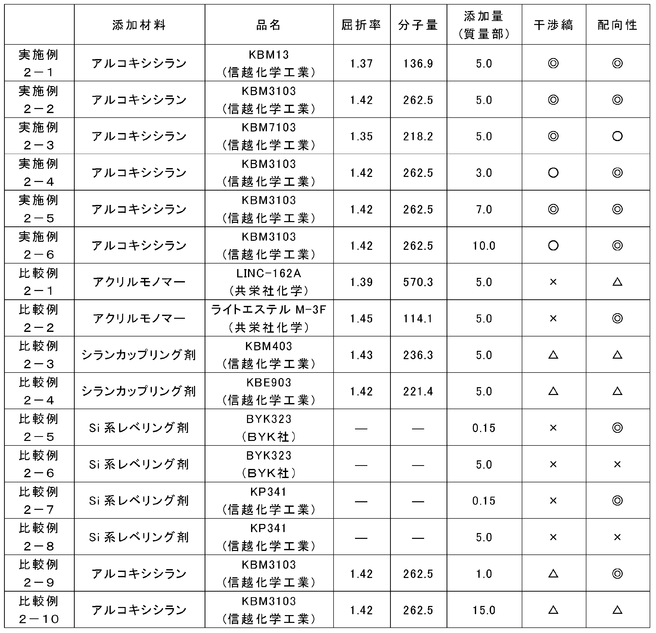
<1.パターン位相差フィルムの構成>
図6は、本発明の第3実施形態に係るパターン位相差フィルム201の一例を示す図である。この実施形態では、このパターン位相差フィルム201により画像表示装置、3D画像表示システムが構成される。
本発明においては、位相差層214が、重合性液晶材料を重合してなる重合液晶と、所定の屈折率を有する微粒子とを含有する。ここで、上記のように、透明基材212の屈折率は、アクリル系透明基材が1.50程度、TAC基材が1.48程度であり、概ね1.45から1.55程度である。一方、重合液晶の屈折率は、1.55から1.75程度と高い。この屈折率差により、位相差層と透明基材との薄膜干渉による干渉縞が発生する。
なお上述した第3の実施形態においては、反射防止層215、透明基材212、配向膜3、重合液晶を含む位相差層214がこの順で積層されてなるパターン位相差フィルム1の態様について説明したが、本発明はこれに限らず、他の実施形態として、図9に拡大断面図を示すように、反射防止層215、重合液晶を含む位相差層214、配向膜3、透明基材212がこの順で積層されてなるパターン位相差フィルム201Aとすることができる。
〔実施例〕
図6、図8の構成のパターン位相差フィルムを作製した。ここで、基材212及び反射防止層215は、アクリルフィルム40μm(屈折率1.50)上に形成されたクリアHC(ハードコート)と低反射防止層の積層体(10μm)である(ヘイズ0.3%)。この反射防止層と反対側の面の透明基材上に、配向層213(日産化学工業WO2011/126022(A)に記載される、光配向性基及びヒドロキシル基を有する化合物(低分子)、(B)ポリマー、架橋剤(C)の混合物)の塗工液をダイコーティングにより塗布乾燥した後、20mJ/cm2の光量による直線偏光による紫外線をパターン照射して厚さ0.1μm程度の配向層213を作製した。このときの直線偏光光は、搬送方向MDに対して±45度の角度を持った光とした。
実施例3-1において、屈折率が1.45で平均粒径2.0μmのシリカ微粒子を固形分質量比で0.5%含有させた以外は実施例3-1と同様にしてパターン位相差フィルムを得た。
実施例3-1において、屈折率が1.40で平均粒径0.07μmの中空シリカ微粒子を固形分質量比で0.1%含有させた以外は実施例3-1と同様にしてパターン位相差フィルムを得た。
図9の拡大断面図に示す構成のパターン位相差フィルムを作製した。すなわち、反射防止層215、位相差層214、配向膜3、透明基材212がこの順で積層されてなるパターン位相差フィルムとしたこと以外は、実施例3-1と同様にして作製した。
実施例3-1において、微粒子を含有させなかった以外は実施例3-1と同様にしてパターン位相差フィルムを得た。
実施例3-1において、微粒子を15%含有させた以外は実施例3-1と同様にしてパターン位相差フィルムを得た。
実施例及び比較例、並びに試験例のパターン位相差フィルムについて、CIE表色系の視認反射率である反射Y値(%):(株)島津製作所製分光光度計(UV-3100PC)を用いて、入射角と反射角がそれぞれ、5度のときの反射Y値(%)を測定した。また、位相差層の表面凹凸測定による表面粗さRa値(表面粗さ測定機SE-3400(小坂研究所製))の評価と、黒アクリル板に位相差層面側を貼合し、蛍光灯下にて反射防止層側からの干渉縞の目視評価、を行った。また、ヘイズメーター(HM-150:村上色彩製)にて位相差層形成後のフィルムのヘイズ(%)を測定した。その結果を表1に示す。

図10は、本発明の第3実施形態に係る位相差フィルム301の一例を示す図である。この実施形態では、この位相差フィルム301により画像表示装置、3D画像表示システムが構成される。
本発明においては、透明基材の屈折率をn1、配向層の屈折率をn2、位相差層の屈折率をn3とした場合に、
n1<n2<n3であって、
n1とn3の平均値であるnAVE=(n1+n3)/2に対して、
nAVE+0.01>n2>nAVE-0.01
を満たすように、前記配向層が形成されていることを特徴としている。すなわち、配向層の屈折率を、透明基材の屈折率と位相差層の屈折率との略中間値とすることで、干渉縞の発生を抑制することができる。
なお上述した第4の実施形態においては、反射防止層315、透明基材312、配向層313、重合液晶を含む位相差層314がこの順で積層されてなるパターン位相差フィルム301の態様について説明したが、本発明はこれに限らず、他の実施形態として、図12に拡大断面図を示すように、反射防止層315、重合液晶を含む位相差層314、配向層313、透明基材312がこの順で積層されてなるパターン位相差フィルム301Aとすることができる。
n1<n2<n3であって、
n1とn3の平均値であるnAVE=(n1+n3)/2に対して、
nAVE+0.01>n2>nAVE-0.01
を満たすように、配向層が形成されていることを特徴としている。このような構成のパターン位相差フィルム301Aによれば、配向層の屈折率を、透明基材の屈折率と位相差層の屈折率との略中間値とすることで、干渉縞の発生を効果的に抑制することができる。
<実施例4-1>
図11(a)の構成のパターン位相差フィルムを作製した。ここで、基材312及び反射防止層315は、アクリルフィルム40μm(屈折率1.50)上に形成されたクリアHC(ハードコート)と低反射防止層の積層体10μm(商品名ReaLook反射率1.0%:日油社製)である。この反射防止層と反対側の面の透明基材上に、配向層313(屈折率1.56の(「ROP-103」(Rolic technologies Ltd.社製)の塗工液をダイコーティングにより塗布乾燥した後、20mJ/cm2の光量による直線偏光による紫外線をパターン照射して厚さ0.1μmの配向層313を作製した。このときの直線偏光光は、搬送方向MDに対して±45度の角度を持った光とした。
実施例4-1において、屈折率1.52の光2量化高分子材料を用い、そこに屈折率が1.57で平均粒径1.5μmの酸化アルミナ微粒子を、屈折率調整微粒子として質量比で1%含有させて配向層全体の屈折率を1.54に調整した以外は実施例4-1と同様にしてパターン位相差フィルムを得た。
図12の拡大断面図に示す構成のパターン位相差フィルムを作製した。すなわち、反射防止層315、位相差層314、配向層313、透明基材312がこの順で積層されてなるパターン位相差フィルムとしたこと以外は、実施例4-1と同様にして作製した。
実施例4-1において、位相差層314として、光重合性ネマチック液晶(重合液晶単独の屈折率1.58)の液晶層組成物(溶剤としてMIBK使用)を単独で用いた以外は実施例4-1と同様にしてパターン位相差フィルムを得た。
実施例4-2において、配向層に微粒子を15%含有させた以外は実施例4-1と同様にしてパターン位相差フィルムを得た。
実施例4-及び比較例のパターン位相差フィルムについて、CIE表色系の視認反射率である反射Y値(%):(株)島津製作所製分光光度計(UV-3100PC)を用いて、入射角と反射角がそれぞれ、5度のときの反射Y値(%)を測定した。黒アクリル板に位相差層面側を貼合し、蛍光灯下にて反射防止層側からの干渉縞の目視評価、を行った。その結果を表1に示す。
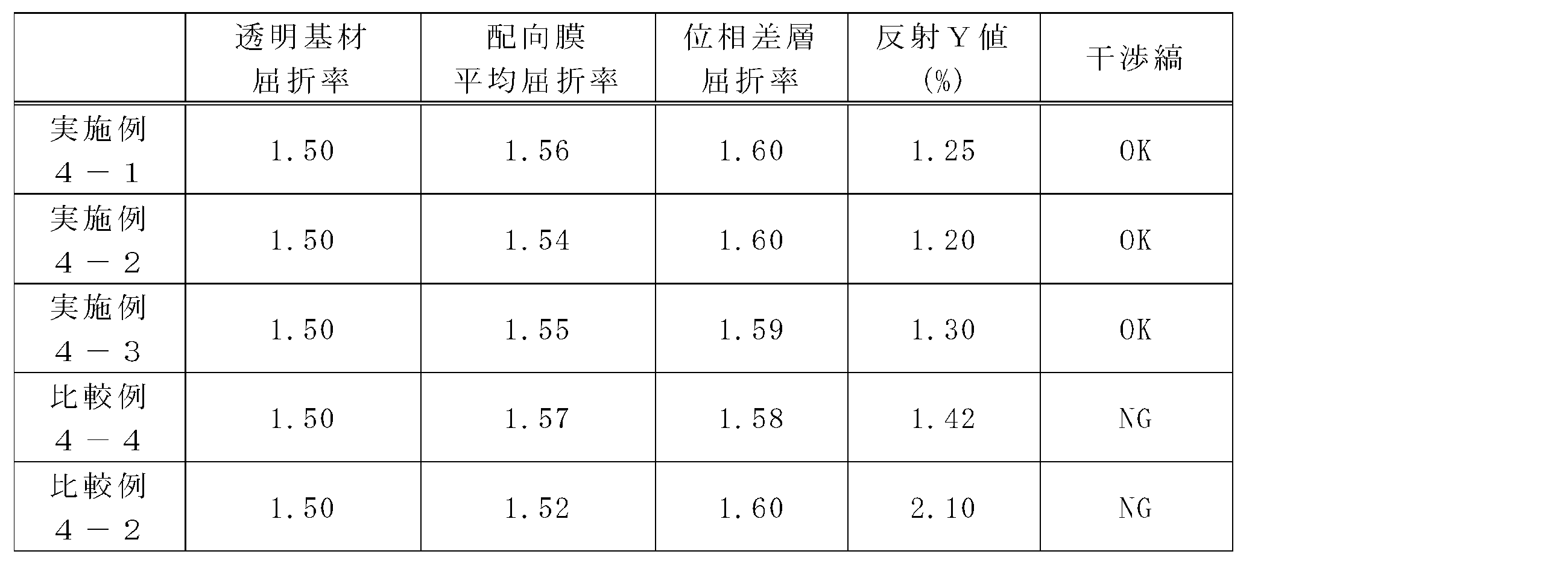
以上、本発明の実施に好適な具体的な構成を詳述したが、本発明は、本発明の趣旨を逸脱しない範囲で、上述の実施形態の構成を種々に変更することができる。
11、111、212、312 基材
12、112、213、313、330 配向層
13、113、214、314 位相差層
214a 微粒子
215、315 反射防止層
330a 添加剤
Claims (37)
- 基材と、光配向材料を含有する配向層と、液晶化合物を含有する位相差層とを含む位相差フィルムであって、
前記配向層は、前記光配向材料100質量部に対し、屈折率1.60以上のエポキシモノマーを3.0質量部以上8.0質量部以下の割合で含有する位相差フィルム。 - 前記エポキシモノマーは、その屈折率が1.70以上である請求項1に記載の位相差フィルム。
- 光軸測定したときの、標準偏差(σ)で定義される光軸の面内バラツキが、1.5未満である請求項1又は請求項2に記載の位相差フィルム。
- 前記配向層が、配向パターンを有する請求項1、請求項2、請求項3の何れかに記載の位相差フィルム。
- 請求項1から請求項4の何れかに記載の位相差フィルムを備える偏光板。
- 請求項1から請求項4の何れかに記載の位相差フィルムを備える画像表示装置。
- 請求項6に記載の画像表示装置を備える3D画像表示システム。
- 基材と、光配向材料を含有する配向層と、液晶化合物を含有する位相差層とを含む位相差フィルムの製造方法であって、
前記光配向材料100質量部に対して屈折率1.60以上のエポキシモノマーを3.0質量部以上8.0質量部以下の割合で含有する配向層組成物を用い、前記基材上に該配向層組成物を塗工して硬化させることで前記配向層を形成する位相差フィルムの製造方法。 - 基材と、配向層と、液晶化合物を含有する位相差層とを含む位相差フィルムであって、
前記位相差層は、前記液晶化合物100質量部に対してアルコキシシランを2.0質量部以上14.0質量部以下の割合で含有する位相差フィルム。 - 前記アルコキシシランの屈折率が1.50以下である請求項9に記載の位相差フィルム。
- 光軸測定したときの、標準偏差(σ)で定義される光軸の面内バラツキが、1.5未満である請求項9又は請求項10に記載の位相差フィルム。
- 前記配向層が、配向パターンを有する請求項9から請求項11の何れかに記載の位相差フィルム。
- 請求項9から請求項12の何れかに記載の位相差フィルムを備える偏光板。
- 請求項9から請求項12の何れかに記載の位相差フィルムを備える画像表示装置。
- 請求項14に記載の画像表示装置を備える3D画像表示システム。
- 基材と、配向層と、液晶化合物を含有する位相差層とを含む位相差フィルムの製造方法であって、
前記液晶化合物100質量部に対してアルコキシシランを2.0質量部以上14.0質量部以下の割合で含有する液晶組成物を用い、前記配向層上に該液晶組成物を塗工して硬化させることで前記位相差層を形成する位相差フィルムの製造方法。 - 反射防止層、透明基材、配向層、重合液晶を含む位相差層、が順次積層されており、前記位相差層により透過光に位相差を与える位相差フィルムであって、
前記反射防止層は、JISK7105によるヘイズ値が0.5%以下のクリア系反射防止層であり、
前記位相差層は、前記重合液晶の屈折率より低い屈折率を有する微粒子を含有することを特徴とする位相差フィルム。 - 前記微粒子の屈折率は1.3以上1.7以下である請求項17に記載の位相差フィルム。
- 前記微粒子の平均粒径は前記位相差層の膜厚より大きい請求項17又は請求項18に記載の位相差フィルム。
- 前記微粒子がシリカであって、前記位相差層中の微粒子の含有量が0.01質量%以上10質量%以下である請求項17から請求項19の何れかに記載の位相差フィルム。
- 前記位相差層の表面粗さRaが3nm以上200nmである請求項17から請求項20の何れかに記載の位相差フィルム。
- 前記透明基材がアクリル系樹脂であり、厚さが80μm以下である請求項17から請求項21の何れかに記載の位相差フィルム。
- 前記配向層が、配向パターンを有する請求項17から請求項22の何れかに記載の位相差フィルム。
- 請求項17から請求項23の何れかに記載の位相差フィルムを備える偏光板。
- 請求項17から請求項23の何れかに記載の位相差フィルムを備える画像表示装置。
- 請求項25に記載の画像表示装置を備える3D画像表示システム。
- 反射防止層、重合液晶を含む位相差層、配向層、透明基材、が順次積層されており、前記位相差層により透過光に位相差を与える位相差フィルムであって、
前記反射防止層は、JISK7105によるヘイズ値が0.5%以下のクリア系反射防止層であり、
前記位相差層は、前記重合液晶の屈折率より低い屈折率を有する微粒子を含有することを特徴とする位相差フィルム。 - 反射防止層、透明基材、配向層、重合液晶を含む位相差層、が順次積層されており、前記位相差層により透過光に位相差を与える位相差フィルムであって、
前記反射防止層は、JISK7105によるヘイズ値が0.5%以下のクリア系反射防止層であり、
前記透明基材の屈折率をn1、前記配向層の屈折率をn2、前記位相差層の屈折率をn3とした場合に、
n1<n2<n3であって、
n1とn3の平均値であるnAVE=(n1+n3)/2に対して、
nAVE+0.01>n2>nAVE-0.01
を満たすことを特徴とする位相差フィルム。 - 前記透明基材が、厚さが80μm以下のアクリル系樹脂である請求項28に記載の位相差フィルム。
- 前記配向層の屈折率n2が1.53以上1.56以下である請求項28又は請求項29に記載の位相差フィルム。
- 前記配向層が、光2量化型の高分子材料で構成されている請求項28から請求項30の何れかに記載の位相差フィルム。
- 前記配向層が、光2量化型の高分子材料と、屈折率を調整する添加剤とを含有する請求項28から請求項31の何れかに記載の位相差フィルム。
- 前記配向層が、配向パターンを有する請求項28から請求項32の何れかに記載の位相差フィルム。
- 請求項28から請求項33の何れかに記載の位相差フィルムを備える偏光板。
- 請求項28から請求項33の何れかに記載の位相差フィルムを備える画像表示装置。
- 請求項35に記載の画像表示装置を備える3D画像表示システム。
- 反射防止層、重合液晶を含む位相差層、配向層、透明基材、が順次積層されており、前記位相差層により透過光に位相差を与える位相差フィルムであって、
前記反射防止層は、JISK7105によるヘイズ値が0.5%以下のクリア系反射防止層であり、
前記透明基材の屈折率をn1、前記配向層の屈折率をn2、前記位相差層の屈折率をn3とした場合に、
n1<n2<n3であって、
n1とn3の平均値であるnAVE=(n1+n3)/2に対して、
nAVE+0.01>n2>nAVE-0.01
を満たすことを特徴とする位相差フィルム。
Priority Applications (4)
| Application Number | Priority Date | Filing Date | Title |
|---|---|---|---|
| JP2015528328A JP6586882B2 (ja) | 2013-07-24 | 2014-07-24 | 位相差フィルム、位相差フィルムの製造方法、この位相差フィルムを用いた偏光板及び画像表示装置、この画像表示装置を使用した3d画像表示システム |
| CN201480031701.XA CN105264408B (zh) | 2013-07-24 | 2014-07-24 | 相位差薄膜及其制造方法、采用其的偏振片及图像显示装置、使用该装置的3d图像显示系统 |
| US14/902,993 US20160139314A1 (en) | 2013-07-24 | 2014-07-24 | Retardation film, method for manufacturing retardation film, polarizing plate and image display device which use retardation film, and 3d image display system using image display device |
| KR1020167000599A KR20160034285A (ko) | 2013-07-24 | 2014-07-24 | 위상차 필름, 위상차 필름의 제조 방법, 이 위상차 필름을 사용한 편광판 및 화상 표시 장치, 이 화상 표시 장치를 사용한 3d 화상 표시 시스템 |
Applications Claiming Priority (12)
| Application Number | Priority Date | Filing Date | Title |
|---|---|---|---|
| JP2013153446 | 2013-07-24 | ||
| JP2013-153446 | 2013-07-24 | ||
| JP2013-154219 | 2013-07-25 | ||
| JP2013154219 | 2013-07-25 | ||
| JP2013188203 | 2013-09-11 | ||
| JP2013-188204 | 2013-09-11 | ||
| JP2013188204 | 2013-09-11 | ||
| JP2013-188203 | 2013-09-11 | ||
| JP2014001868 | 2014-01-08 | ||
| JP2014001869 | 2014-01-08 | ||
| JP2014-001868 | 2014-01-08 | ||
| JP2014-001869 | 2014-01-08 |
Publications (1)
| Publication Number | Publication Date |
|---|---|
| WO2015012347A1 true WO2015012347A1 (ja) | 2015-01-29 |
Family
ID=52393381
Family Applications (1)
| Application Number | Title | Priority Date | Filing Date |
|---|---|---|---|
| PCT/JP2014/069543 Ceased WO2015012347A1 (ja) | 2013-07-24 | 2014-07-24 | 位相差フィルム、位相差フィルムの製造方法、この位相差フィルムを用いた偏光板及び画像表示装置、この画像表示装置を使用した3d画像表示システム |
Country Status (6)
| Country | Link |
|---|---|
| US (1) | US20160139314A1 (ja) |
| JP (1) | JP6586882B2 (ja) |
| KR (1) | KR20160034285A (ja) |
| CN (1) | CN105264408B (ja) |
| TW (1) | TW201510584A (ja) |
| WO (1) | WO2015012347A1 (ja) |
Cited By (3)
| Publication number | Priority date | Publication date | Assignee | Title |
|---|---|---|---|---|
| JP2016170315A (ja) * | 2015-03-13 | 2016-09-23 | 日本電信電話株式会社 | 領域分割波長板およびその製造方法 |
| KR20230108880A (ko) * | 2022-01-12 | 2023-07-19 | 삼성에스디아이 주식회사 | 액정 위상차 필름, 편광판 및 광학 표시 장치 |
| WO2025094817A1 (ja) * | 2023-10-31 | 2025-05-08 | 富士フイルム株式会社 | 光学積層体、積層光学フィルムおよび光学物品 |
Families Citing this family (5)
| Publication number | Priority date | Publication date | Assignee | Title |
|---|---|---|---|---|
| CN103885229B (zh) * | 2014-03-07 | 2017-01-11 | 京东方科技集团股份有限公司 | 一种液晶面板及其制作方法、3d显示装置 |
| CN105116625B (zh) * | 2015-09-23 | 2018-01-02 | 京东方科技集团股份有限公司 | 一种液晶光取向的控制方法 |
| JP6748920B2 (ja) * | 2017-03-13 | 2020-09-02 | 日本電気硝子株式会社 | ガラスフィルムの製造方法 |
| CN106918863B (zh) | 2017-05-12 | 2019-09-13 | 京东方科技集团股份有限公司 | 相位膜基板及其制造方法和显示装置 |
| US12276884B1 (en) * | 2023-10-31 | 2025-04-15 | The Hong Kong University Of Science And Technology | Electrically switchable liquid crystal grating cell based on photoalignment with an amplitude mask |
Citations (5)
| Publication number | Priority date | Publication date | Assignee | Title |
|---|---|---|---|---|
| JP2005049865A (ja) * | 2003-07-17 | 2005-02-24 | Arisawa Mfg Co Ltd | 光学位相差素子の製造方法 |
| JP2009300698A (ja) * | 2008-06-12 | 2009-12-24 | Sony Chemical & Information Device Corp | 液晶性位相差フィルムの製造方法、及び液晶表示装置 |
| JP2010286597A (ja) * | 2009-06-10 | 2010-12-24 | Dainippon Printing Co Ltd | 位相差板 |
| JP2012237928A (ja) * | 2011-05-13 | 2012-12-06 | Fujifilm Corp | 光学フィルム、偏光板、画像表示装置及び3d画像表示システム |
| JP2013057803A (ja) * | 2011-09-08 | 2013-03-28 | Dic Corp | 光配向性基板、光学異方体及び液晶表示素子 |
Family Cites Families (5)
| Publication number | Priority date | Publication date | Assignee | Title |
|---|---|---|---|---|
| TWI383191B (zh) * | 2004-05-07 | 2013-01-21 | Fujifilm Corp | 液晶顯示裝置 |
| JP2010026097A (ja) * | 2008-07-16 | 2010-02-04 | Sekisui Chem Co Ltd | 位相差フィルム、複合偏光板、偏光板および液晶表示装置 |
| JP5581180B2 (ja) * | 2010-11-10 | 2014-08-27 | 大阪ガスケミカル株式会社 | フルオレン骨格を有するエポキシ樹脂組成物およびその硬化物 |
| TWI465483B (zh) * | 2010-12-28 | 2014-12-21 | Chi Mei Corp | 液晶配向劑,液晶配向膜,及含有該液晶配向膜的液晶顯示元件 |
| US9151869B2 (en) * | 2011-01-25 | 2015-10-06 | Lg Chem, Ltd. | Liquid crystal film |
-
2014
- 2014-07-24 CN CN201480031701.XA patent/CN105264408B/zh active Active
- 2014-07-24 US US14/902,993 patent/US20160139314A1/en not_active Abandoned
- 2014-07-24 TW TW103125296A patent/TW201510584A/zh unknown
- 2014-07-24 JP JP2015528328A patent/JP6586882B2/ja active Active
- 2014-07-24 KR KR1020167000599A patent/KR20160034285A/ko not_active Withdrawn
- 2014-07-24 WO PCT/JP2014/069543 patent/WO2015012347A1/ja not_active Ceased
Patent Citations (5)
| Publication number | Priority date | Publication date | Assignee | Title |
|---|---|---|---|---|
| JP2005049865A (ja) * | 2003-07-17 | 2005-02-24 | Arisawa Mfg Co Ltd | 光学位相差素子の製造方法 |
| JP2009300698A (ja) * | 2008-06-12 | 2009-12-24 | Sony Chemical & Information Device Corp | 液晶性位相差フィルムの製造方法、及び液晶表示装置 |
| JP2010286597A (ja) * | 2009-06-10 | 2010-12-24 | Dainippon Printing Co Ltd | 位相差板 |
| JP2012237928A (ja) * | 2011-05-13 | 2012-12-06 | Fujifilm Corp | 光学フィルム、偏光板、画像表示装置及び3d画像表示システム |
| JP2013057803A (ja) * | 2011-09-08 | 2013-03-28 | Dic Corp | 光配向性基板、光学異方体及び液晶表示素子 |
Cited By (4)
| Publication number | Priority date | Publication date | Assignee | Title |
|---|---|---|---|---|
| JP2016170315A (ja) * | 2015-03-13 | 2016-09-23 | 日本電信電話株式会社 | 領域分割波長板およびその製造方法 |
| KR20230108880A (ko) * | 2022-01-12 | 2023-07-19 | 삼성에스디아이 주식회사 | 액정 위상차 필름, 편광판 및 광학 표시 장치 |
| KR102886878B1 (ko) | 2022-01-12 | 2025-11-14 | 삼성에스디아이 주식회사 | 액정 위상차 필름, 편광판 및 광학 표시 장치 |
| WO2025094817A1 (ja) * | 2023-10-31 | 2025-05-08 | 富士フイルム株式会社 | 光学積層体、積層光学フィルムおよび光学物品 |
Also Published As
| Publication number | Publication date |
|---|---|
| TW201510584A (zh) | 2015-03-16 |
| JPWO2015012347A1 (ja) | 2017-03-02 |
| US20160139314A1 (en) | 2016-05-19 |
| KR20160034285A (ko) | 2016-03-29 |
| CN105264408B (zh) | 2019-11-05 |
| CN105264408A (zh) | 2016-01-20 |
| JP6586882B2 (ja) | 2019-10-09 |
Similar Documents
| Publication | Publication Date | Title |
|---|---|---|
| JP6586882B2 (ja) | 位相差フィルム、位相差フィルムの製造方法、この位相差フィルムを用いた偏光板及び画像表示装置、この画像表示装置を使用した3d画像表示システム | |
| CN103842858B (zh) | 长条型图案取向膜及使用其的长条型图案相位差薄膜 | |
| JP5720795B2 (ja) | パターン位相差フィルム及びその製造方法 | |
| KR20180097453A (ko) | 광학 필름 및 그 제조 방법 | |
| KR20190027826A (ko) | 타원 편광판 | |
| TWI799570B (zh) | 偏光板 | |
| JP7513136B2 (ja) | 位相差フィルム、偏光板補償フィルム、及び外光反射防止フィルム | |
| JPWO2018146995A1 (ja) | 加飾フィルム | |
| JP2020134678A (ja) | 位相差層積層偏光板およびそれを用いた画像表示装置 | |
| JP6724297B2 (ja) | 光学積層体の製造方法、円偏光板の製造方法及び有機エレクトロルミネッセンス表示装置の製造方法 | |
| KR20220012288A (ko) | 화상 표시 장치의 제조 방법 및 편광자 전사용 적층체 | |
| JP5545262B2 (ja) | 発光型表示装置 | |
| JP2015052679A (ja) | 位相差フィルム及びその製造方法 | |
| JP6287371B2 (ja) | 光学フィルム、光学フィルム用転写体、及び画像表示装置 | |
| JP2015068949A (ja) | 位相差フィルム及びその製造方法、偏光板、並びに、画像表示装置 | |
| JP6697216B2 (ja) | 位相差フィルム | |
| JP2012073514A (ja) | 位相差フィルム、偏光子付き位相差フィルム、積層型パターン位相差板、および液晶表示装置 | |
| TWI548896B (zh) | 長型圖案配向膜及使用其之長型圖案相位差薄膜 | |
| JP2014119569A (ja) | パターン位相差フィルム及びその製造方法 | |
| JP2013076762A (ja) | パターン配向層用組成物、並びにパターン配向膜及びパターン位相差フィルムの製造方法 | |
| JP6830914B2 (ja) | 光学フィルム、光学フィルム用転写体、及び画像表示装置 | |
| JP2016191874A (ja) | 光学フィルム | |
| JP5780268B2 (ja) | 三次元表示用途のパターン位相差フィルム | |
| JP2015084074A (ja) | 位相差フィルム | |
| JPWO2013128692A1 (ja) | 長尺パターン配向膜およびそれを用いた長尺パターン位相差フィルム |
Legal Events
| Date | Code | Title | Description |
|---|---|---|---|
| WWE | Wipo information: entry into national phase |
Ref document number: 201480031701.X Country of ref document: CN |
|
| 121 | Ep: the epo has been informed by wipo that ep was designated in this application |
Ref document number: 14829776 Country of ref document: EP Kind code of ref document: A1 |
|
| WWE | Wipo information: entry into national phase |
Ref document number: 14902993 Country of ref document: US |
|
| ENP | Entry into the national phase |
Ref document number: 20167000599 Country of ref document: KR Kind code of ref document: A |
|
| ENP | Entry into the national phase |
Ref document number: 2015528328 Country of ref document: JP Kind code of ref document: A |
|
| NENP | Non-entry into the national phase |
Ref country code: DE |
|
| 122 | Ep: pct application non-entry in european phase |
Ref document number: 14829776 Country of ref document: EP Kind code of ref document: A1 |