WO2015001900A1 - 弾性波デバイス - Google Patents
弾性波デバイス Download PDFInfo
- Publication number
- WO2015001900A1 WO2015001900A1 PCT/JP2014/064945 JP2014064945W WO2015001900A1 WO 2015001900 A1 WO2015001900 A1 WO 2015001900A1 JP 2014064945 W JP2014064945 W JP 2014064945W WO 2015001900 A1 WO2015001900 A1 WO 2015001900A1
- Authority
- WO
- WIPO (PCT)
- Prior art keywords
- acoustic wave
- wave device
- substrate
- piezoelectric substrate
- elastic wave
- Prior art date
- Legal status (The legal status is an assumption and is not a legal conclusion. Google has not performed a legal analysis and makes no representation as to the accuracy of the status listed.)
- Ceased
Links
Images


Classifications
-
- H—ELECTRICITY
- H03—ELECTRONIC CIRCUITRY
- H03H—IMPEDANCE NETWORKS, e.g. RESONANT CIRCUITS; RESONATORS
- H03H9/00—Networks comprising electromechanical or electro-acoustic elements; Electromechanical resonators
- H03H9/25—Constructional features of resonators using surface acoustic waves
-
- H—ELECTRICITY
- H03—ELECTRONIC CIRCUITRY
- H03H—IMPEDANCE NETWORKS, e.g. RESONANT CIRCUITS; RESONATORS
- H03H9/00—Networks comprising electromechanical or electro-acoustic elements; Electromechanical resonators
- H03H9/02—Details
- H03H9/02535—Details of surface acoustic wave devices
- H03H9/02637—Details concerning reflective or coupling arrays
- H03H9/02669—Edge reflection structures, i.e. resonating structures without metallic reflectors, e.g. Bleustein-Gulyaev-Shimizu [BGS], shear horizontal [SH], shear transverse [ST], Love waves devices
-
- H—ELECTRICITY
- H03—ELECTRONIC CIRCUITRY
- H03H—IMPEDANCE NETWORKS, e.g. RESONANT CIRCUITS; RESONATORS
- H03H9/00—Networks comprising electromechanical or electro-acoustic elements; Electromechanical resonators
- H03H9/02—Details
- H03H9/02535—Details of surface acoustic wave devices
- H03H9/02543—Characteristics of substrate, e.g. cutting angles
- H03H9/02574—Characteristics of substrate, e.g. cutting angles of combined substrates, multilayered substrates, piezoelectrical layers on not-piezoelectrical substrate
-
- H—ELECTRICITY
- H03—ELECTRONIC CIRCUITRY
- H03H—IMPEDANCE NETWORKS, e.g. RESONANT CIRCUITS; RESONATORS
- H03H9/00—Networks comprising electromechanical or electro-acoustic elements; Electromechanical resonators
- H03H9/02—Details
- H03H9/125—Driving means, e.g. electrodes, coils
- H03H9/145—Driving means, e.g. electrodes, coils for networks using surface acoustic waves
Definitions
- the present invention relates to an acoustic wave device.
- an end face reflection type acoustic wave device using reflection of an elastic wave at a substrate end face.
- an elastic wave excited by an IDT (Interdigital-Transducer) electrode formed on a piezoelectric substrate propagates to the end surface of the substrate and is reflected by the end surface.
- IDT Interdigital-Transducer
- Such an end surface reflection type acoustic wave device is manufactured as follows, for example. That is, first, a disk-shaped piezoelectric wafer and a support wafer having a smaller coefficient of thermal expansion than that of the piezoelectric wafer are bonded to produce a disk-shaped composite wafer.
- the composite wafer is cut into rectangular regions by a cutting device such as a dicing saw.
- a cutting device such as a dicing saw.
- an elastic wave device including a substantially rectangular parallelepiped composite substrate in which the piezoelectric substrate and the support substrate are joined and an IDT electrode formed on the piezoelectric substrate is obtained.
- the reason why the composite substrate is used is to suppress the change in the frequency characteristic with respect to the temperature change of the acoustic wave device by reducing the change in the size of the piezoelectric substrate when the temperature changes.
- Patent Documents 1 and 2 employ the following manufacturing method. That is, in Patent Document 1, (1) a cutting groove is provided by a dicing saw around a rectangular area before forming an IDT electrode, and (2) the surface of the piezoelectric wafer is then polished to perform chipping near the opening of the cutting groove. (3) Next, an IDT electrode is formed, and (4) an acoustic wave device is then cut out using a dicing saw having a narrower width than the cutting groove.
- Patent Document 2 (1) IDT electrodes are formed on each of a large number of rectangular regions provided on a piezoelectric wafer of a composite wafer. (2) Next, a piezoelectric wafer is formed from the support wafer side by laser activation. A procedure is adopted in which cutting is made for each rectangular region to a depth that does not reach, and (3) the elastic wave device is cut by applying stress that divides the supporting wafer.
- Patent Documents 1 and 2 describe that the spurious is suppressed by removing the chipping of the end face where the elastic wave is reflected, that is, the end face orthogonal to the elastic wave propagation direction, the elastic wave propagation direction is described.
- the end face parallel to is not considered.
- the present inventors reflect that unnecessary elastic waves are reflected at this end surface, which increases spurious. I found it.
- the present invention has been made to solve such problems, and has as its main object to more reliably suppress spurious in an end face reflection type elastic wave device.
- the acoustic wave device of the present invention is An end face reflection type acoustic wave device in which a pair of IDT electrodes are disposed on the piezoelectric substrate of the substantially rectangular parallelepiped composite substrate in which the support substrate and the piezoelectric substrate are joined,
- the chipping size of the first side surface orthogonal to the elastic wave propagation direction among the side surfaces of the piezoelectric substrate is 1/10 or less of the wavelength ⁇ of the elastic wave
- the chipping size of the second side surface parallel to the elastic wave propagation direction among the side surfaces of the piezoelectric substrate is larger than the chipping size of the first side surface and is not less than 1/2 and not more than 50 times the wavelength ⁇ of the elastic wave. Is.
- the chipping size of the first side surface where the elastic wave having a desired wavelength is reflected is 1/10 or less of the wavelength ⁇ of the elastic wave, the amount of reflection on the first side surface is sufficiently high.
- the phase change of the elastic wave due to the displacement of the position of the first side surface hardly occurs, the occurrence of spurious due to the phase change can be suppressed.
- the chipping size of the second side surface is larger than the chipping size of the first side surface and is 1 ⁇ 2 or more and 50 times or less of the wavelength ⁇ of the elastic wave, the elastic wave of unnecessary wavelength is difficult to be reflected on the second side surface, Also in this respect, generation of spurious can be suppressed.
- the chipping size of the second side surface is less than 1 ⁇ 2 of the wavelength ⁇ , it is not preferable because an elastic wave having an unnecessary wavelength is easily reflected on the second side surface and spurious is easily generated.
- the chipping size of the second side surface exceeds 50 times the wavelength ⁇ , it is not preferable because the Q value of the resonator is deteriorated.
- the chipping size of the second side surface is preferably 12.5 times to 50 times the wavelength ⁇ of the acoustic wave.
- the support substrate preferably has a smaller thermal expansion coefficient than the piezoelectric substrate. By doing so, it is possible to reduce the change in the size of the piezoelectric substrate when the temperature changes, and to suppress the change in the frequency characteristic with respect to the temperature change of the acoustic wave device.
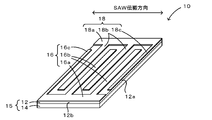
- FIG. 1 is a perspective view of an acoustic wave device 10.
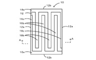
- FIG. FIG. 2 is a plan view of the acoustic wave device 10.
- FIG. 3 is a cross-sectional view taken along line AA in FIG. 2.
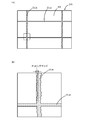
- FIG. 3 is a perspective view showing a manufacturing flow of the acoustic wave device 10. Explanatory drawing of dicing.
- FIG. 1 and 2 are a perspective view and a plan view of the acoustic wave device 10 of the present embodiment
- FIG. 3 is a cross-sectional view taken along the line AA of FIG.
- the acoustic wave device 10 is an end surface reflection type acoustic wave device, and a pair of IDT electrodes 16 and 18 are provided on a piezoelectric substrate 12 of a substantially rectangular parallelepiped composite substrate 15 in which a piezoelectric substrate 12 and a support substrate 14 are joined. They are arranged so as to enter each other.
- the piezoelectric substrate 12 is a substrate capable of propagating surface acoustic waves (SAW).
- SAW surface acoustic waves
- LT or LN is preferred. This is because LT and LN have high SAW propagation speed and a large electromechanical coupling coefficient, and are therefore suitable as high-frequency and wideband frequency acoustic wave devices.
- the thickness of the piezoelectric substrate 12 is not particularly limited, but may be 0.2 to 50 ⁇ m, for example.
- the piezoelectric substrate 12 has a first side surface 12a orthogonal to the elastic wave propagation direction (SAW propagation direction) and a second side surface 12b parallel to the SAW propagation direction. If the wavelength of the excited SAW is ⁇ , and the distance between the first side surfaces 12a facing each other is L (see FIG. 3), L is designed to be an integral multiple of ⁇ / 2.
- the support substrate 14 has a smaller thermal expansion coefficient than the piezoelectric substrate 12 and is bonded to the back surface of the piezoelectric substrate 12 by direct bonding or via an organic adhesive layer.
- the support substrate 14 has a coefficient of thermal expansion smaller than that of the piezoelectric substrate 12, a change in the size of the piezoelectric substrate 12 when the temperature changes is suppressed, and the composite substrate 15 is used for the acoustic wave device 10.
- the temperature change of the frequency characteristic can be suppressed.
- Examples of the material of the support substrate 14 include silicon, sapphire, aluminum nitride, alumina, borosilicate glass, and quartz glass. Silicon or sapphire is preferable.
- the thickness of the support substrate 14 is not particularly limited, but may be, for example, 200 to 1200 ⁇ m.
- the composite substrate 15 is obtained by bonding the piezoelectric substrate 12 and the support substrate 14 together.
- the bonding may be direct bonding or indirect bonding that is bonded via an organic adhesive layer.
- Such a composite substrate 15 is a substantially rectangular parallelepiped, and the size thereof is not particularly limited.
- the length and width may be 1 mm ⁇ 2 mm or 2 mm ⁇ 2.5 mm.
- the IDT electrode 16 includes a base portion 16a parallel to the SAW propagation direction, a wide electrode finger 16b extending from the base portion 16a in a direction orthogonal to the SAW propagation direction, and a SAW propagation extending from the base portion 16a in a direction orthogonal to the SAW propagation direction.
- a narrow electrode finger 16c disposed at the end in the direction.
- the IDT electrode 18 includes a base portion 18a, a wide electrode finger 18b, and a narrow electrode finger 18c. Both IDT electrodes 16 and 18 are spaced apart so as not to contact each other.
- one of the two wide electrode fingers 16b of the IDT electrode 16 is disposed so as to enter between two adjacent wide electrode fingers 18b of the IDT electrode 18, and the other is formed of the wide electrode finger 18b.
- the narrow electrode finger 18c is ⁇ / 8.
- the SAW having the wavelength ⁇ excited by the IDT electrodes 16 and 18 propagates to the first side surface 12a of the piezoelectric substrate 12 and is reflected by the first side surface 12a.
- the chipping size of the first side surface 12a is 1/10 or less of the SAW wavelength ⁇
- the amount of reflection at the first side surface 12a is sufficiently high.
- the surface accuracy of the first side surface 12a is high, the phase change of the SAW due to the displacement of the position of the first side surface 12a is difficult to occur, so that the occurrence of spurious due to the phase change can be suppressed.
- the chipping size of the second side surface 12b is larger than the chipping size of the first side surface 12a, specifically, it is not less than 1/2 and not more than 50 times the wavelength ⁇ . Therefore, the SAW having an unnecessary wavelength is difficult to be reflected by the second side surface 12b, and spurious generation can be suppressed also in this respect.
- FIG. 4 is a perspective view showing a manufacturing flow of the acoustic wave device 10.
- a disk-shaped piezoelectric wafer 22 having an orientation flat (OF) and a support wafer 24 having the same shape are prepared (see FIG. 4A).
- the bonding surfaces of both wafers 22 and 24 are washed to remove dirt adhering to the bonding surfaces.
- an inert gas such as argon
- the remaining impurities oxide film, adsorbed material, etc.
- the wafers 22 and 24 are bonded together after being aligned in vacuum so that the OFs of the wafers 22 and 24 match at room temperature (see FIG. 4B).
- the surface of the piezoelectric wafer 22 is polished to a predetermined thickness to complete the composite wafer 25 (see FIG. 4C).
- an electrode for an acoustic wave device is formed on the surface of the piezoelectric wafer 22 in the composite wafer 25.
- the surface of the piezoelectric wafer 22 is partitioned so that a large number of acoustic wave devices are formed, and the IDT electrodes 16 and 18 described above are formed at a position corresponding to each acoustic wave device by using a photolithography technique.
- a large number of acoustic wave devices 10 are obtained by dicing the composite wafer 25 along the section (see FIG. 4D).
- FIG. 5 is an explanatory view of dicing, (a) is a plan view of the composite wafer 25, and (b) is an enlarged view of a portion surrounded by a dotted line in (a).
- the blade is selected and cut so that the cut surface of the cut line CLa that becomes the first side surface 12 a of the acoustic wave device 10 has a chipping size of 1/10 or less of the wavelength ⁇ .
- the cut surface of the cut line CLb that becomes the second side surface 12b of the acoustic wave device 10 can be adjusted in rotation speed, feed rate, roughness, thickness, etc. so that the chipping size is 1 ⁇ 2 to 50 times the wavelength ⁇ . Select different blades and cut.
- the chipping size refers to the maximum value of the unevenness on the cut surface.
- the chipping size of the first side surface 12a reflected by the SAW having the desired wavelength ⁇ is 1/10 or less of the wavelength ⁇ of the SAW.
- the amount of reflection is sufficiently high.
- the chipping size of the second side surface 12b is larger than the chipping size of the first side surface 12a (specifically, not less than 1/2 and not more than 50 times the wavelength ⁇ ), an unnecessary wavelength SAW is reflected by the second side surface 12b. It is difficult to suppress the occurrence of spurious.
- the cut line CLa and the cut line CLb are cut using a blade, but may be cut using a laser activation method.
- the laser irradiation conditions may be set so as to match the chipping size of each of the cut lines CLa and CLb.
- the chipping size may be increased by roughening the cut surface of the cut line CLb with a file or the like.
- the piezoelectric wafer 22 and the support wafer 24 are bonded together by direct bonding using an ion beam.
- a method using plasma or a neutral atom beam may be adopted. .
- the piezoelectric wafer 22 and the support wafer 24 are bonded together by direct bonding, but may be bonded via an organic adhesive layer.
- the organic adhesive may be uniformly applied to one or both of the front surface of the support substrate 14 and the back surface of the piezoelectric substrate 12, and the organic adhesive may be solidified in a state where they are overlapped.
- Example 1 As a piezoelectric wafer, a disc-shaped 42 ° Y-cut X-propagation LT substrate (thickness 250 ⁇ m) having a SAW propagation direction X and a cutting angle of a rotating Y-cut plate was prepared. In addition, a disc-shaped Si (111) substrate (thickness: 230 ⁇ m) was prepared as a support wafer. Both wafers were put into a vacuum chamber of 2 ⁇ 10 ⁇ 6 (Pa), and the surface was irradiated with an argon beam for 60 seconds.
- the irradiated surfaces of both wafers were brought into contact with each other, pressurized with 2000 kg, and both wafers were bonded by direct bonding.
- the joined body was taken out from the vacuum chamber, and the LT surface was ground to 30 ⁇ m. Then, it grind
- IDT electrodes were formed on a large number of rectangular regions (2 mm ⁇ 1 mm) on the LT surface of the composite wafer by a photolithographic process, and diced to the size of the rectangular regions to obtain a large number of acoustic wave devices.
- the design value of the wavelength ⁇ of the SAW was 4 ⁇ m.
- Dicing was performed using a blade.
- the blade cut along the direction orthogonal to the SAW propagation direction (cut line CLa in FIG. 5) was cut using a thickness of 0.05 mm and # 2000 at a rotation speed of 29000 rpm and a feed rate of 20 mm / s.
- a blade cut along a direction parallel to the SAW propagation direction (cut line CLb in FIG.
- Example 5 was a blade having a thickness of 0.1 mm and # 500, and was cut at a rotational speed of 29000 rpm and a feed rate of 50 mm / s.
- the chipping size of the first side surface orthogonal to the SAW propagation direction is 0.4 ⁇ m (0.1 times ⁇ )
- the chipping size of the second side surface parallel to the SAW propagation direction is 50 ⁇ m ( ⁇ of 12 .5 times).
- Table 1 The data for Example 1 is summarized in Table 1.
- Example 2 In the same manner as in Example 1, a composite wafer on which IDT electrodes were formed was produced. This composite wafer was diced under the processing conditions shown in Example 2 of Table 1. The obtained acoustic wave device had a first side chipping size of 0.4 ⁇ m (0.1 times ⁇ ) and a second side chipping size of 2 ⁇ m (0.5 times ⁇ ).
- Example 3 In the same manner as in Example 1, a composite wafer on which IDT electrodes were formed was produced. This composite wafer was diced under the processing conditions shown in Example 3 of Table 1. The obtained acoustic wave device had a first side chipping size of 0.4 ⁇ m (0.1 times ⁇ ) and a second side chipping size of 200 ⁇ m (50 times ⁇ ).
- Comparative Example 1 In the same manner as in Example 1, a composite wafer on which IDT electrodes were formed was produced. This composite wafer was diced under the processing conditions shown in Comparative Example 1 of Table 1. The chipping sizes of the first and second side surfaces of the obtained acoustic wave device were both 10 ⁇ m or less, specifically 0.4 ⁇ m (0.1 times ⁇ ).
- Example 2 In the same manner as in Example 1, a composite wafer on which IDT electrodes were formed was produced. This composite wafer was diced under the processing conditions shown in Comparative Example 2 of Table 1. The obtained elastic wave device had a first side chipping size of 0.4 ⁇ m (0.1 times ⁇ ) and a second side chipping size of 240 ⁇ m (60 times ⁇ ).
- Example 3 In the same manner as in Example 1, a composite wafer on which IDT electrodes were formed was produced. This composite wafer was diced under the processing conditions shown in Comparative Example 3 of Table 1. The resulting acoustic wave device had a first side chipping size of 2.0 ⁇ m (0.5 times ⁇ ) and a second side chipping size of 50 ⁇ m (12.5 times ⁇ ).
- the present invention can be used for an acoustic wave device such as a SAW filter.
- 10 acoustic wave device 12 piezoelectric substrate, 12a first side, 12b second side, 14 support substrate, 15 composite substrate, 16, 18 IDT electrode, 16a, 18a base, 16b, 18b wide electrode fingers, 16c, 18c width Narrow electrode fingers, 22 piezoelectric wafers, 24 support wafers, 25 composite wafers.
Landscapes
- Physics & Mathematics (AREA)
- Acoustics & Sound (AREA)
- Surface Acoustic Wave Elements And Circuit Networks Thereof (AREA)
Abstract
Description
支持基板と圧電基板とが接合された略直方体の複合基板のうちの前記圧電基板上に一対のIDT電極が互いに入り込むように配置された端面反射型の弾性波デバイスであって、
前記圧電基板の側面のうち弾性波伝搬方向と直交する第1側面のチッピングサイズは、弾性波の波長λの1/10以下であり、
前記圧電基板の側面のうち弾性波伝搬方向と平行な第2側面のチッピングサイズは、前記第1側面のチッピングサイズより大きく、弾性波の波長λの1/2以上50倍以下である、
ものである。
圧電ウェハーとして、SAWの伝搬方向をXとし、切り出し角が回転Yカット板である円盤状の42°YカットX伝搬LT基板(厚さ250μm)を用意した。また、支持ウェハーとして、円盤状のSi(111)基板(厚さ230μm)を用意した。両ウェハーを2×10-6(Pa)の真空チャンバーに投入し、アルゴンビームを表面に60秒照射した。照射後、両ウェハーの照射面同士をコンタクトさせ、2000kgで加圧し、直接接合により両ウェハーを接合した。接合体を真空チャンバーから取り出し、LT面を30μmまで研削した。その後、ダイヤモンドスラリー(粒径1μm)を滴下しながら錫定盤で25μmまで研磨した。更に、コロイダルシリカ(粒径20nm)を滴下しながら、ウレタンパッドで20μmまで研磨して、弾性波デバイス用の複合ウェハーとした。続いて、フォトリソプロセスで、複合ウェハーのLT表面上の多数の矩形領域(2mm×1mm)にIDT電極を形成し、その矩形領域のサイズにダイシングして多数の弾性波デバイスを得た。SAWの波長λの設計値は、4μmとした。ダイシングはブレードを用いて行った。SAW伝搬方向と直交する方向(図5のカットラインCLa)に沿って切断するブレードは、厚さ0.05mm、#2000を用い、回転数29000rpm、送り速度20mm/sで切断した。SAW伝搬方向と平行な方向(図5のカットラインCLb)に沿って切断するブレードは、厚さ0.1mm、#500のブレードを用い、回転数29000rpm、送り速度50mm/sで切断した。得られた弾性波デバイスのSAW伝搬方向と直交する第1側面のチッピングサイズは0.4μm(λの0.1倍)、SAW伝搬方向と平行な第2側面のチッピングサイズは50μm(λの12.5倍)であった。実施例1に関するデータを表1にまとめた。
実施例1と同様にして、IDT電極が形成された複合ウェハーを作製した。この複合ウェハーを、表1の実施例2に示す加工条件でダイシングを行った。得られた弾性波デバイスの第1側面のチッピングサイズは0.4μm(λの0.1倍)、第2側面のチッピングサイズは2μm(λの0.5倍)であった。
実施例1と同様にして、IDT電極が形成された複合ウェハーを作製した。この複合ウェハーを、表1の実施例3に示す加工条件でダイシングを行った。得られた弾性波デバイスの第1側面のチッピングサイズは0.4μm(λの0.1倍)、第2側面のチッピングサイズは200μm(λの50倍)であった。
実施例1と同様にして、IDT電極が形成された複合ウェハーを作製した。この複合ウェハーを、表1の比較例1に示す加工条件でダイシングを行った。得られた弾性波デバイスの第1及び第2側面のチッピングサイズは、いずれも10μm以下、具体的には0.4μm(λの0.1倍)であった。
実施例1と同様にして、IDT電極が形成された複合ウェハーを作製した。この複合ウェハーを、表1の比較例2に示す加工条件でダイシングを行った。得られた弾性波デバイスの第1側面のチッピングサイズは0.4μm(λの0.1倍)、第2側面のチッピングサイズは240μm(λの60倍)であった。
実施例1と同様にして、IDT電極が形成された複合ウェハーを作製した。この複合ウェハーを、表1の比較例3に示す加工条件でダイシングを行った。得られた弾性波デバイスの第1側面のチッピングサイズは2.0μm(λの0.5倍)、第2側面のチッピングサイズは50μm(λの12.5倍)であった。

実施例1~3及び比較例1~3について、1ポート共振器の特性を評価した。そうしたところ、スプリアスピークの強度は、表1に示すように、実施例1~3では2~2.7dBであったのに対して、比較例1~3では5~7dBであった。この結果から、第1側面のチッピングサイズを弾性波の波長λの1/10以下、第2側面のチッピングサイズを弾性波の波長λの1/2以上50倍以下(特に12.5倍以上50倍以下)とすることがスプリアスの発生を抑制するうえで好ましいことがわかった。
Claims (3)
- 支持基板と圧電基板とが接合された略直方体の複合基板のうちの前記圧電基板上に一対のIDT電極が互いに入り込むように配置された端面反射型の弾性波デバイスであって、
前記圧電基板の側面のうち弾性波伝搬方向と直交する第1側面のチッピングサイズは、弾性波の波長λの1/10以下であり、
前記圧電基板の側面のうち弾性波伝搬方向と平行な第2側面のチッピングサイズは、前記第1側面のチッピングサイズより大きく、弾性波の波長λの1/2以上50倍以下である、
弾性波デバイス。 - 前記第2側面のチッピングサイズは、弾性波の波長λの12.5倍以上50倍以下である、
請求項1に記載の弾性波デバイス。 - 前記支持基板は、前記圧電基板よりも熱膨張係数が小さい、
請求項1又は2に記載の弾性波デバイス。
Priority Applications (5)
| Application Number | Priority Date | Filing Date | Title |
|---|---|---|---|
| JP2015525107A JP6426089B2 (ja) | 2013-07-02 | 2014-06-05 | 弾性波デバイス |
| KR1020157036233A KR102254964B1 (ko) | 2013-07-02 | 2014-06-05 | 탄성파 디바이스 |
| DE112014003124.0T DE112014003124B4 (de) | 2013-07-02 | 2014-06-05 | Schallwellenvorrichtung |
| CN201480036216.1A CN105340178B (zh) | 2013-07-02 | 2014-06-05 | 弹性波装置 |
| US14/978,055 US10230349B2 (en) | 2013-07-02 | 2015-12-22 | Acoustic wave device |
Applications Claiming Priority (2)
| Application Number | Priority Date | Filing Date | Title |
|---|---|---|---|
| JP2013138588 | 2013-07-02 | ||
| JP2013-138588 | 2013-07-02 |
Related Child Applications (1)
| Application Number | Title | Priority Date | Filing Date |
|---|---|---|---|
| US14/978,055 Continuation US10230349B2 (en) | 2013-07-02 | 2015-12-22 | Acoustic wave device |
Publications (1)
| Publication Number | Publication Date |
|---|---|
| WO2015001900A1 true WO2015001900A1 (ja) | 2015-01-08 |
Family
ID=52143486
Family Applications (1)
| Application Number | Title | Priority Date | Filing Date |
|---|---|---|---|
| PCT/JP2014/064945 Ceased WO2015001900A1 (ja) | 2013-07-02 | 2014-06-05 | 弾性波デバイス |
Country Status (7)
| Country | Link |
|---|---|
| US (1) | US10230349B2 (ja) |
| JP (1) | JP6426089B2 (ja) |
| KR (1) | KR102254964B1 (ja) |
| CN (1) | CN105340178B (ja) |
| DE (1) | DE112014003124B4 (ja) |
| TW (1) | TWI613844B (ja) |
| WO (1) | WO2015001900A1 (ja) |
Cited By (2)
| Publication number | Priority date | Publication date | Assignee | Title |
|---|---|---|---|---|
| JP2020009804A (ja) * | 2018-07-03 | 2020-01-16 | 日東電工株式会社 | 封止用シートおよび電子素子装置の製造方法 |
| WO2020050396A1 (ja) * | 2018-09-06 | 2020-03-12 | 京セラ株式会社 | 複合基板、圧電素子および複合基板の製造方法 |
Families Citing this family (7)
| Publication number | Priority date | Publication date | Assignee | Title |
|---|---|---|---|---|
| TWD174921S (zh) * | 2014-12-17 | 2016-04-11 | 日本碍子股份有限公司 | 複合基板之部分 |
| JP2018042208A (ja) * | 2016-09-09 | 2018-03-15 | 株式会社ディスコ | 表面弾性波デバイスチップの製造方法 |
| US10848121B2 (en) | 2016-10-14 | 2020-11-24 | Qorvo Us, Inc. | Guided SAW device |
| US10924085B2 (en) * | 2016-10-17 | 2021-02-16 | Qorvo Us, Inc. | Guided acoustic wave device |
| TWI604641B (zh) * | 2016-11-09 | 2017-11-01 | Crystalwise Tech Inc | Acoustic wave device and its composite substrate |
| GB2608902B (en) * | 2018-08-22 | 2023-05-17 | Skyworks Solutions Inc | Multilayer piezolelectric substrate |
| JP2020182035A (ja) * | 2019-04-23 | 2020-11-05 | 株式会社ディスコ | Sawフィルタの製造方法及びsawフィルタ |
Citations (5)
| Publication number | Priority date | Publication date | Assignee | Title |
|---|---|---|---|---|
| JPS6213020U (ja) * | 1985-07-05 | 1987-01-26 | ||
| JPH0486114A (ja) * | 1990-07-30 | 1992-03-18 | Murata Mfg Co Ltd | 表面波装置 |
| JPH04298113A (ja) * | 1991-03-27 | 1992-10-21 | Toshiba Corp | 弾性表面波デバイスおよびその製造方法 |
| JP2002009583A (ja) * | 2000-06-26 | 2002-01-11 | Matsushita Electric Ind Co Ltd | 圧電デバイス及びその製造方法 |
| JP2009118504A (ja) * | 1999-06-14 | 2009-05-28 | Panasonic Corp | 弾性表面波素子 |
Family Cites Families (6)
| Publication number | Priority date | Publication date | Assignee | Title |
|---|---|---|---|---|
| JPH0823260A (ja) * | 1994-07-11 | 1996-01-23 | Oki Electric Ind Co Ltd | 弾性表面波共振器 |
| JP3106912B2 (ja) * | 1995-06-30 | 2000-11-06 | 株式会社村田製作所 | 端面反射型表面波装置の製造方法 |
| JP2002261559A (ja) | 2001-02-28 | 2002-09-13 | Toyo Commun Equip Co Ltd | 端面反射型表面波装置の製造方法 |
| JP3760378B2 (ja) * | 2001-09-14 | 2006-03-29 | 株式会社村田製作所 | 端面反射型表面波装置及びその製造方法 |
| JP2004336503A (ja) * | 2003-05-09 | 2004-11-25 | Fujitsu Media Device Kk | 弾性表面波素子及びその製造方法 |
| CN202998019U (zh) * | 2012-11-08 | 2013-06-12 | 日本碍子株式会社 | 弹性波滤波器及具备该弹性波滤波器的弹性波装置 |
-
2014
- 2014-06-05 DE DE112014003124.0T patent/DE112014003124B4/de active Active
- 2014-06-05 CN CN201480036216.1A patent/CN105340178B/zh active Active
- 2014-06-05 WO PCT/JP2014/064945 patent/WO2015001900A1/ja not_active Ceased
- 2014-06-05 JP JP2015525107A patent/JP6426089B2/ja active Active
- 2014-06-05 KR KR1020157036233A patent/KR102254964B1/ko active Active
- 2014-06-06 TW TW103119668A patent/TWI613844B/zh active
-
2015
- 2015-12-22 US US14/978,055 patent/US10230349B2/en active Active
Patent Citations (5)
| Publication number | Priority date | Publication date | Assignee | Title |
|---|---|---|---|---|
| JPS6213020U (ja) * | 1985-07-05 | 1987-01-26 | ||
| JPH0486114A (ja) * | 1990-07-30 | 1992-03-18 | Murata Mfg Co Ltd | 表面波装置 |
| JPH04298113A (ja) * | 1991-03-27 | 1992-10-21 | Toshiba Corp | 弾性表面波デバイスおよびその製造方法 |
| JP2009118504A (ja) * | 1999-06-14 | 2009-05-28 | Panasonic Corp | 弾性表面波素子 |
| JP2002009583A (ja) * | 2000-06-26 | 2002-01-11 | Matsushita Electric Ind Co Ltd | 圧電デバイス及びその製造方法 |
Cited By (5)
| Publication number | Priority date | Publication date | Assignee | Title |
|---|---|---|---|---|
| JP2020009804A (ja) * | 2018-07-03 | 2020-01-16 | 日東電工株式会社 | 封止用シートおよび電子素子装置の製造方法 |
| JP7110011B2 (ja) | 2018-07-03 | 2022-08-01 | 日東電工株式会社 | 封止用シートおよび電子素子装置の製造方法 |
| WO2020050396A1 (ja) * | 2018-09-06 | 2020-03-12 | 京セラ株式会社 | 複合基板、圧電素子および複合基板の製造方法 |
| JPWO2020050396A1 (ja) * | 2018-09-06 | 2021-08-30 | 京セラ株式会社 | 複合基板、圧電素子および複合基板の製造方法 |
| JP7163395B2 (ja) | 2018-09-06 | 2022-10-31 | 京セラ株式会社 | 複合基板、圧電素子および複合基板の製造方法 |
Also Published As
| Publication number | Publication date |
|---|---|
| TWI613844B (zh) | 2018-02-01 |
| CN105340178B (zh) | 2018-10-19 |
| JP6426089B2 (ja) | 2018-11-21 |
| US10230349B2 (en) | 2019-03-12 |
| JPWO2015001900A1 (ja) | 2017-02-23 |
| TW201519483A (zh) | 2015-05-16 |
| KR102254964B1 (ko) | 2021-05-24 |
| KR20160026890A (ko) | 2016-03-09 |
| DE112014003124T5 (de) | 2016-04-21 |
| DE112014003124B4 (de) | 2025-06-26 |
| US20160112029A1 (en) | 2016-04-21 |
| CN105340178A (zh) | 2016-02-17 |
Similar Documents
| Publication | Publication Date | Title |
|---|---|---|
| JP6426089B2 (ja) | 弾性波デバイス | |
| EP2736169B1 (en) | Composite substrate, elastic surface wave device, and method for producing composite substrate | |
| KR102183134B1 (ko) | 접합체 및 탄성파 소자 | |
| JP3187231U (ja) | 複合基板 | |
| JP5850137B2 (ja) | 弾性波装置及びその製造方法 | |
| JP6567970B2 (ja) | 複合基板の製法 | |
| US8847469B2 (en) | Composite substrate and method for manufacturing the composite substrate | |
| CN105027436B (zh) | 复合基板、弹性波装置及弹性波装置的制造方法 | |
| TWI780103B (zh) | 彈性波元件及其製造方法 | |
| KR20150034715A (ko) | 복합 기판, 압전 디바이스 및 복합 기판의 제법 | |
| SG181225A1 (en) | Acoustic wave device | |
| JP6646058B2 (ja) | 接合基板及びその製造方法とこの接合基板を用いた弾性表面波デバイス | |
| JP6247054B2 (ja) | 弾性波デバイス及びその製法 | |
| JP2021158553A (ja) | 弾性波デバイスおよびその製造方法、フィルタ、マルチプレクサおよびウエハ | |
| JP4863097B2 (ja) | 弾性表面波素子の製造方法 | |
| JP2018093329A (ja) | 弾性波素子 | |
| CN116366017A (zh) | 声波器件、晶圆和制造晶圆的方法 | |
| JP2010251827A (ja) | 弾性表面波素子 |
Legal Events
| Date | Code | Title | Description |
|---|---|---|---|
| WWE | Wipo information: entry into national phase |
Ref document number: 201480036216.1 Country of ref document: CN |
|
| 121 | Ep: the epo has been informed by wipo that ep was designated in this application |
Ref document number: 14820428 Country of ref document: EP Kind code of ref document: A1 |
|
| ENP | Entry into the national phase |
Ref document number: 2015525107 Country of ref document: JP Kind code of ref document: A |
|
| ENP | Entry into the national phase |
Ref document number: 20157036233 Country of ref document: KR Kind code of ref document: A |
|
| WWE | Wipo information: entry into national phase |
Ref document number: 112014003124 Country of ref document: DE |
|
| 122 | Ep: pct application non-entry in european phase |
Ref document number: 14820428 Country of ref document: EP Kind code of ref document: A1 |
|
| WWG | Wipo information: grant in national office |
Ref document number: 112014003124 Country of ref document: DE |