WO2014208048A1 - Pilote de diode laser, dispositif d'amplification de lumière directe, système de transmission de signal lumineux et procédé de pilotage de diode laser - Google Patents
Pilote de diode laser, dispositif d'amplification de lumière directe, système de transmission de signal lumineux et procédé de pilotage de diode laser Download PDFInfo
- Publication number
- WO2014208048A1 WO2014208048A1 PCT/JP2014/003245 JP2014003245W WO2014208048A1 WO 2014208048 A1 WO2014208048 A1 WO 2014208048A1 JP 2014003245 W JP2014003245 W JP 2014003245W WO 2014208048 A1 WO2014208048 A1 WO 2014208048A1
- Authority
- WO
- WIPO (PCT)
- Prior art keywords
- laser diode
- excitation
- optical
- output
- current
- Prior art date
Links
Images


Classifications
-
- H—ELECTRICITY
- H01—ELECTRIC ELEMENTS
- H01S—DEVICES USING THE PROCESS OF LIGHT AMPLIFICATION BY STIMULATED EMISSION OF RADIATION [LASER] TO AMPLIFY OR GENERATE LIGHT; DEVICES USING STIMULATED EMISSION OF ELECTROMAGNETIC RADIATION IN WAVE RANGES OTHER THAN OPTICAL
- H01S5/00—Semiconductor lasers
- H01S5/06—Arrangements for controlling the laser output parameters, e.g. by operating on the active medium
- H01S5/068—Stabilisation of laser output parameters
- H01S5/06825—Protecting the laser, e.g. during switch-on/off, detection of malfunctioning or degradation
-
- H—ELECTRICITY
- H04—ELECTRIC COMMUNICATION TECHNIQUE
- H04B—TRANSMISSION
- H04B10/00—Transmission systems employing electromagnetic waves other than radio-waves, e.g. infrared, visible or ultraviolet light, or employing corpuscular radiation, e.g. quantum communication
- H04B10/03—Arrangements for fault recovery
-
- H—ELECTRICITY
- H04—ELECTRIC COMMUNICATION TECHNIQUE
- H04B—TRANSMISSION
- H04B10/00—Transmission systems employing electromagnetic waves other than radio-waves, e.g. infrared, visible or ultraviolet light, or employing corpuscular radiation, e.g. quantum communication
- H04B10/29—Repeaters
- H04B10/291—Repeaters in which processing or amplification is carried out without conversion of the main signal from optical form
-
- H—ELECTRICITY
- H01—ELECTRIC ELEMENTS
- H01S—DEVICES USING THE PROCESS OF LIGHT AMPLIFICATION BY STIMULATED EMISSION OF RADIATION [LASER] TO AMPLIFY OR GENERATE LIGHT; DEVICES USING STIMULATED EMISSION OF ELECTROMAGNETIC RADIATION IN WAVE RANGES OTHER THAN OPTICAL
- H01S5/00—Semiconductor lasers
- H01S5/04—Processes or apparatus for excitation, e.g. pumping, e.g. by electron beams
- H01S5/042—Electrical excitation ; Circuits therefor
-
- H—ELECTRICITY
- H01—ELECTRIC ELEMENTS
- H01S—DEVICES USING THE PROCESS OF LIGHT AMPLIFICATION BY STIMULATED EMISSION OF RADIATION [LASER] TO AMPLIFY OR GENERATE LIGHT; DEVICES USING STIMULATED EMISSION OF ELECTROMAGNETIC RADIATION IN WAVE RANGES OTHER THAN OPTICAL
- H01S5/00—Semiconductor lasers
- H01S5/06—Arrangements for controlling the laser output parameters, e.g. by operating on the active medium
- H01S5/068—Stabilisation of laser output parameters
- H01S5/0683—Stabilisation of laser output parameters by monitoring the optical output parameters
-
- H—ELECTRICITY
- H01—ELECTRIC ELEMENTS
- H01S—DEVICES USING THE PROCESS OF LIGHT AMPLIFICATION BY STIMULATED EMISSION OF RADIATION [LASER] TO AMPLIFY OR GENERATE LIGHT; DEVICES USING STIMULATED EMISSION OF ELECTROMAGNETIC RADIATION IN WAVE RANGES OTHER THAN OPTICAL
- H01S5/00—Semiconductor lasers
- H01S5/40—Arrangement of two or more semiconductor lasers, not provided for in groups H01S5/02 - H01S5/30
- H01S5/4018—Lasers electrically in series
Definitions
- the present invention relates to a laser diode driving device, an optical direct amplification device, an optical signal transmission system, and a laser diode driving method.
- the present invention relates to a laser diode driving device for an optical direct amplifier used in a long-distance optical signal transmission system such as a submarine cable system.
- a plurality of pumping laser diodes (hereinafter referred to as LDs) are mounted on an optical direct amplifier used in a long-distance optical signal transmission system laid on the seabed (LD: Laser Diode).
- LD Laser Diode
- a general optical direct amplifying apparatus has a configuration in which only the current pumping LD is mounted and driven. For this reason, when some of the pumping LDs fail, there is a problem that the total pumping LD intensity decreases and the output of the optical direct amplifier decreases.
- Patent Document 1 discloses a laser diode drive circuit that controls the flow of a bias current bypassing an LD whose light output is low when the light output of the LD is equal to or less than a predetermined value.
- Patent Document 2 discloses a method for driving a pumping light source for optical amplification, in which a plurality of light sources for pumping light that are input into an optical fiber together with signal light to amplify the light are provided, and a deteriorated operating light source is replaced with a standby light source. It is disclosed.
- the pumping light source for optical amplification of Patent Document 2 has a problem that the total light output changes when the deteriorated light source is replaced with a light source on standby.
- the laser diode driving device of the present invention includes driving means for controlling driving of a predetermined laser diode according to the output state of a plurality of laser diodes connected in series between two power supplies.
- the laser diode driving method of the present invention controls driving of a predetermined laser diode according to the output state of a plurality of laser diodes connected in series between two power supplies.
- the present invention it is possible to provide a laser diode driving device in which the overall excitation laser diode intensity does not change even when any of the current excitation laser diodes is switched to a spare excitation laser diode. it can.
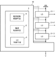
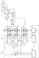
- FIG. 1 shows a laser diode driving apparatus 10 according to an outline of an embodiment of the present invention.
- the laser diode driving device 10 is a laser diode driving circuit that drives a plurality of laser diodes 31 connected in series between two power sources.
- FIG. 1 shows an example in which a plurality of laser diodes 31 are constituted by three laser diodes 31-1 to 31-3.
- the laser diode driving apparatus 10 includes driving means 3 that controls driving of a predetermined laser diode in accordance with the output state of the plurality of laser diodes 31.
- the laser diodes 31-1 and 31-2 are driven as working LDs
- the laser diode 31-3 is a predetermined laser diode (LD: Laser Diode).
- the predetermined laser diode is a spare LD that is used in place of the LD that cannot be used when any of the current LDs cannot be used due to a failure or the like.
- the predetermined laser diode is included in the plurality of laser diodes 31.
- the driving means 3 includes a current path control means 4, a current control means 5, and a laser diode control means 6 (LD control means 6 in FIG. 1).
- the current path control means 4 receives a signal corresponding to the output of each laser diode as input, and controls the current control means 5 according to the input signal.
- the current control means 5 receives a signal corresponding to the output of each laser diode, and controls the current supplied to each laser diode in accordance with the input signal.
- Laser diode control means 6 receives a signal corresponding to the output of each laser diode as input, and controls the current supplied between the two power supplies.
- the laser diode driving apparatus 10 According to the laser diode driving apparatus 10 according to the present embodiment described above, there is no change in the overall excitation laser diode intensity even when the excitation laser diode is switched. Therefore, in the optical direct amplification device using the laser diode driving device according to the present embodiment, the output does not change even when the excitation laser diode is switched.
- the laser diode driving device 10 according to the present embodiment will be described in more detail below.
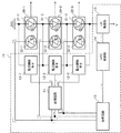
- the excitation LD drive circuit 10 includes a logic circuit 11, a bypass current control element 12 (12-1, 12-2, 12-3), an adder circuit 13, and an APC.
- the control part 14 and the LD drive part 15 are provided (APC: Automatic Power Control).
- the logic circuit 11 in FIG. 2 corresponds to the current path control means 4 in FIG.
- the current control element 12 in FIG. 2 corresponds to the current control means 5 in FIG.
- the adding circuit 13, the APC control unit 14, and the LD driving unit 15 in FIG. 2 are included in the driving unit 3 in FIG.
- the addition circuit 13 is also called addition means
- the APC control unit 14 is also called output control means
- the LD drive unit 15 is also called laser diode drive means.
- the excitation LD drive circuit 10 includes an excitation LD 31 (31-1, 31-2, 31-3) and a built-in PD 32 (32-1, 32-2, 32-3).
- the outputs of a plurality of pumping LD modules 30 (30-1, 30-2, 30-3) having (PD) are controlled (PD: Photodiode).
- the light output of the plurality of excitation LDs 31 is converted into a current value by the built-in PD 32 provided for each excitation LD 31.
- the output (signal) from each built-in PD 32 corresponds to the optical output of the corresponding excitation LD 31, and the total value of these outputs (signals) is the sum of the optical outputs from the plurality of excitation LD modules 30 (both the total output). Can be monitored).
- the optical outputs of the plurality of excitation LDs 31 may be detected not by a method of detecting a signal converted into a current value by the built-in PD 32 but by another method.
- the pumping LD modules 30-1 and 30-2 are used as active and the pumping LD module 30-3 is used as a backup.
- the configuration of the three-stage excitation LD 31 is illustrated, but it may be configured with four or more stages of excitation LD 31, or may be configured with two-stage excitation LD 31. May be.
- the logic circuit 11 receives outputs from the three built-in PDs 32 as inputs.
- the logic circuit 11 is connected to a plurality of bypass current control elements 12 connected in the subsequent stage, and controls the bypass current control elements 12.
- the logic circuit 11 is a current path control unit that takes the output of each excitation LD 31 as an input and controls the operation of each excitation LD 31 according to the output of each excitation LD 31.
- the logic circuit 11 controls the current value bypassed to the bypass current control element 12 with the use of the excitation LD 31. For example, when the output of the excitation LD 31 is sufficient, the current value bypassed to the bypass current control element 12 is increased, and when the output of the excitation LD 31 is insufficient, the current value bypassed to the bypass current control element 12 is increased. What is necessary is just to set so that it may become small. Note that the current value bypassed when the current excitation LD 31 is being driven is generally smaller than the current value bypassed to stop the spare excitation LD 31.
- the logic circuit 11 bypasses the bypass current control element 12 connected in parallel to the spare excitation LD 31. -3 is controlled.
- the current bypassed by the bypass current control element 12-3 is supplied to the spare excitation LD 31 by the control of the logic circuit 11.
- the spare excitation LD 31 emits light.
- the logic circuit 11 controls the bypass current control element 12 (12-1 or 12-2) connected in parallel to the excitation LD 31 (31-1 or 31-2) whose output is reduced.
- the bypass current control element 12 connected in parallel to the excitation LD 31 whose output is reduced bypasses the current supplied to the excitation LD 31 whose output is reduced, and the current excitation LD 31 whose output is reduced is stopped. To do.
- the logic circuit 11 executes drive control of the preliminary excitation LD 31-3 and stop control of the excitation LD 31 whose output is reduced. Note that the drive control and stop control by the logic circuit 11 may be executed sequentially or simultaneously.
- the bypass current control elements 12 (12-1, 12-2, 12-3) are connected to the plurality of pumping LD modules 30 (30-1, 30-2, 30-3) in parallel. It is an element.
- the bypass current control element 12 is installed at the subsequent stage of the logic circuit 10 and bypasses the current according to the output of the corresponding excitation LD 31.
- the bypass current control elements 12 (12-1, 12-2) operate according to the control from the logic circuit 11 when the output of the current excitation LD module 30 (30-1, 30-2) decreases. To do.
- the bypass current control element 12-3 connected to the spare excitation LD module 30-3 bypasses the current, and the excitation LD 31-3 is stopped. Electric power can be suppressed.
- the bypass current control element 12 When the bypass current control element 12 performs a bypass operation, the current supplied to the corresponding excitation LD module 30 is diverted to the bypass current control element 12. In other words, the bypass current control element 12 bypasses the current corresponding to the excitation LD 31 or the spare excitation LD 31-3 whose output has decreased. As a result, the excitation LD module 30 that is OFF does not generate a voltage drop due to the excitation LD 31, and is driven with the voltage distribution of two always operating. Therefore, compared with a pumping LD module having a configuration in which the pumping LD module 30-3 as a spare is not provided, the voltage distribution is the same as that in the general configuration, although one pumping LD is added in series. It is possible to control with.
- bypass current control element 12 performs a bypass operation, a small amount of current is assumed to flow through the corresponding excitation LD 31, but there is a problem if the bypassed excitation LD 31 does not emit light. Absent. Further, in the laser diode driving apparatus 10 of the present embodiment, a switch or a circuit that cuts off a very small amount of current flowing into the excitation LD 31 that is bypassed may be configured.
- the addition circuit 13 is addition means for inputting a signal obtained by converting the optical output of the excitation LD 31 into an electrical signal by the built-in PD 32.
- the signal input to the adder circuit 13 is the same as the signal input to the logic circuit 11.
- the adder circuit 13 receives the outputs from the built-in PDs 32 of the three excitation LD modules 30, calculates the total output (total output) of those outputs, and outputs a signal related to the total output to the APC control unit 14.
- the APC control unit 14 is an output control unit of the excitation LD module 30 and is an output control unit that controls the LD driving unit 15 in accordance with a signal from the addition circuit 13. Normally, a signal relating to the total output (total output value) of all the excitation LD modules 30 is input from the adder circuit 13. The APC control unit 14 controls the LD driving unit 15 so that the total output of the excitation LD module 30 is constant.
- the LD driving unit 15 is a laser diode driving unit that controls the pumping LD 31 included in the pumping LD module 30 according to a control signal from the APC control unit 14 so that the total output from the pumping LD module 30 is constant. It is.
- the LD driving unit 15 is connected in series with a three-stage excitation LD 31 between two power sources as shown in FIG.
- the LD driving unit 15 side (lower part) is set to the voltage V
- the excitation LD 31-1 side (upper part) is grounded (0 V).
- the power supply terminal and the ground terminal of the voltage V are called power supplies
- the power supply terminal and the ground terminal of the voltage V are called between power supplies.
- the LD drive unit 15 drives the current excitation LDs 31-1 and 31-2.
- the spare excitation LD 31-3 is not driven because the current is bypassed by the current control element 15-3 connected in parallel. Even if the spare excitation LD 31-3 is not driven, a current may flow through the excitation LD 31-3 as long as the excitation LD 31-3 does not emit light.
- the spare excitation LD 31-3 is driven.
- the LD driving unit 15 does not need to perform an operation of switching any of the excitation LDs 31-1 and 31-2 to the excitation LD 31-3, and in response to a control signal from the APC control unit 14, What is necessary is just to continue performing the control which drives LD31.
- the present invention is not limited to the above-described configuration.
- the circuit is configured to monitor the optical output of the pumping LD 31, detect a decrease in the output of the pumping LD 31 based on the variation of the monitored light output value, and operate the spare pumping LD 31, the present invention It is included in the range.
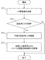
- the excitation LD drive circuit 10 In the excitation LD drive circuit 10 according to the present embodiment, two (30-1 and 30-2) of the three excitation LD modules 30 are driven as active. Further, it is assumed that the spare excitation LD module 30-3 is not driven in the initial state.
- the output of the built-in PD 32 of each excitation LD module 30 is subjected to current / voltage conversion and output to the adder circuit 13.
- the APC control unit 14 controls the LD drive unit 15 so that the total output of the two excitation LDs 31-1 and 31-2 calculated by the adder circuit 13 is constant (step S11).
- the logic circuit 11 When the current excitation LD 31 (31-1 or 31-2) fails and the output decreases (Yes in step S12), the logic circuit 11 is configured so that the spare excitation LD 31-3 is driven.
- the bypass current control element 12-3 is controlled (step S13). Specifically, the logic circuit 11 controls the current value bypassed by the bypass current control element 12-3 to be small, and a current sufficient for the excitation LD 31-3 to emit light is generated. -3.
- the APC control unit 14 performs control so that the total output of the excitation LD module 30 is constant.
- the logic circuit 11 performs control to operate the bypass current control element 12 (12-1 or 12-2) connected in parallel to the failed excitation LD 31 (31-1 or 31-2) (step S1). S14). Specifically, the logic circuit 11 performs control to increase the current value bypassed to the bypass current control element 12 connected in parallel to the failed excitation LD 31. At this time, the current supplied to the failed excitation LD 31 is bypassed by the bypass current control element 12, and the failed excitation LD 31 stops. As a result, even if any one of the current excitation LDs 31 fails, the total output of the excitation LD 31 is controlled to be constant.
- the excitation LD drive circuit As described above, in the excitation LD drive circuit according to the first embodiment of the present invention, when the current excitation LD fails, the spare excitation LD is started and the failed excitation LD is stopped. Thus, the output of the optical direct amplifier is not changed. As a result, it is possible to improve the reliability of the optical direct amplifying device equipped with the pumping LD drive circuit according to the present embodiment, and further the optical signal transmission system provided with the optical direct amplifying device.
- the excitation LD drive circuit according to the first embodiment of the present invention is particularly useful as an excitation LD drive circuit for an optical direct amplifying apparatus installed in a submarine cable system or the like that is difficult to repair after installation. is there.
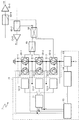
- the optical direct amplifying apparatus 1 includes an LD driving circuit 10, a pumping LD module 30, a polarization combining coupler 40, a 3 dB coupler 50, a WDM coupler 60, and an optical amplifier 70 (WDM: Wavelength Division Multiplexing).
- excitation LD drive circuit 10 and the excitation LD module 30 are the same as those in the first embodiment, description thereof is omitted.
- the polarization beam combiner 40 receives the optical output from the current pumping LD 31 and multiplexes the input optical outputs.
- the optical signal combined by the polarization beam combiner 40 is output to the 3 dB coupler 50.
- the combined output of the polarization combining coupler 40 is half, that is, one pumping LD 31.
- the 3 dB coupler 50 is a branching coupler that branches the optical output combined by the polarization beam combining coupler 40 toward the upstream / downstream transmission path.
- Each of the optical signals branched by the 3 dB coupler 50 has an intensity equivalent to one excitation LD 31.
- the WDM couplers 60-1 and 60-2 each output an optical signal having the intensity of one excitation LD 31.
- the 3 dB coupler 50 When one of the current pumping LDs 31 fails, the 3 dB coupler 50 also receives the optical output from the spare pumping LD 31-3. Therefore, as in the case where the current pumping LD 31 is not out of order, an optical signal having an intensity equivalent to one pumping LD 31 is output to each of the WDM couplers 60-1 and 60-2.
- the WDM couplers 60 are wavelength division multiplexing couplers that input the optical output of the 3 dB coupler 50, combine and demultiplex, and output the demultiplexed light to the optical amplifier 70. .
- the optical amplifiers 70 are optical direct amplifiers that receive the optical signal from the WDM coupler 60 and output the optical signal in the upstream / downstream transmission path.
- the optical amplifier 70 an optical fiber in which rare earth ions such as trivalent erbium are added to quartz fiber can be used.
- the output of the optical amplifier 70 does not decrease. For this reason, the excitation LD intensity input to the optical amplifier 70 is always equal to the output of one excitation LD 31.
- the above is the description of the configuration of the optical direct amplification device 1 according to the second embodiment of the present invention.
- the configuration of the embodiment shown in FIG. 4 is an example, and does not limit the scope of the present invention.
- the output of the built-in PD 32 of each excitation LD module 30 is subjected to current / voltage conversion and output to the adder circuit 13.
- the APC control unit 14 controls the LD driving unit 15 in the adding circuit 13 so that the total output of the two excitation LDs 31-1 and 31-2 is constant (step S21).
- the polarization beam combiner 40 multiplexes the optical outputs of the pumping LDs 31-1 and 31-2. This is output to the 3 dB coupler 50 (step S23).
- the 3 dB coupler 50 receives the optical output of the polarization beam combining coupler 40, and outputs an optical signal branched toward the upstream / downstream transmission path via the WDM coupler 60 and the optical amplifier 70 (step S24).
- the logic circuit 11 drives the spare pumping LD 31-3.
- the bypass control element 12-3 is controlled (step S25). That is, the logic circuit 11 performs control to reduce the current value bypassed to the bypass control element 12-3 and to supply the excitation LD 31-3 with a current sufficient for the excitation LD 31-3 to emit light. I do.
- the APC control unit 14 performs control so that the total output of the excitation LD module 30 is constant.
- Step S26 the logic circuit 11 performs control to bypass current to the bypass current control element 12 (12-1 or 12-2) connected in parallel to the failed excitation LD 31 (31-1 or 31-2).
- Step S26 the logic circuit 11 performs control such that current is bypassed to the bypass current control element 12.
- the malfunctioning excitation LD 31 stops operating.
- steps S25 and S26 controls the total output of the excitation LD 31 to be constant even when any one of the current excitation LDs 31 breaks down.
- the polarization beam combiner 40 receives the optical output from the pumping LD 31 that is not out of the current pumping LDs 31, and multiplexes / demultiplexes the input optical output (step S27).
- the 3 dB coupler 50 receives the optical output of the polarization combining coupler 40 and also receives the optical output of the spare excitation LD 31-3, and multiplexes / demultiplexes the two optical outputs (step S28).
- the 3 dB coupler 50 outputs an optical signal toward the upstream / downstream transmission path via the WDM coupler 60 and the optical amplifier 70 (step S29).
- the optical output of the pumping LD 31 is multiplexed by the polarization beam combining coupler 40 and then the up / down signal is output by the 3 dB coupler 50. It is demultiplexed toward the transmission line.
- the excitation LD intensity input to the optical amplifier 70 of each transmission line is equal to the output of one excitation LD 31.
- the output of the optical amplifier 70 does not decrease even when the current pumping LD 31 fails.
- the excitation LD drive circuit 101 in FIG. 6 is configured to mount and drive only the current excitation LD 31 (31-1, 31-2).
- the excitation LD drive circuit 101 includes a constant current source unit 110, two APC control units 114 (114-1, 114-2), and two LD drive units 115 (115-1, 115-2). I have.
- the constant current source unit 110 is connected in series with the excitation LD 31 (31-1, 31-2) and supplies a constant current to the excitation LD 31.
- the APC control unit 114 (114-1, 114-2) detects the optical output of the excitation LD 31 (31-1, 31-2) included in each excitation LD module 30 (30-1, 30-2).
- the output of the built-in PD 32 (32-1, 32-2) is input.
- the APC control unit 114 controls the LD driving unit 115 according to the output of the built-in PD 32.
- the LD driving unit 115 drives the excitation LD 31 in accordance with the control of each APC control unit 114.
- the 3 dB coupler 50 combines the optical outputs of the pumping LDs 31 and outputs optical signals to the WDM couplers 60 (60-1 and 60-2) in the upstream / downstream transmission path.
- the WDM coupler 60 receives the output of the WDM coupler 60 (60-1, 60-2) and outputs it to the optical amplifier 70 (70-1, 70-2).
- the optical amplifier 70 receives the output of the WDM coupler 60 (60-1, 60-2), amplifies it, and then outputs the amplified optical signal to the upstream / downstream transmission path.
- the total pumping LD intensity is halved. That is, since the optical output input to the 3 dB coupler 50 is reduced, the output of the optical amplifier 70 is reduced.
- the output drop due to the failure mode is recovered after several relays. Therefore, even if one of the excitation LDs fails, there is no major problem in the system.
- the constant pumping light intensity control method it is necessary to use a highly reliable pumping LD, and there is a problem that the cost of the transmission line system including the optical direct amplifying device increases.
- the optical direct amplifying device using the excitation LD drive circuit according to the present embodiment even if a general excitation LD is used, if the excitation LD fails, a spare excitation LD Therefore, the output of the optical direct amplifying device does not decrease.
- a general excitation LD drive circuit it is necessary to provide an LD drive circuit for each excitation LD.
- an operation is performed with a single LD drive circuit. It becomes possible to make it. That is, according to the embodiment of the present invention, the configuration of the circuit / device is simplified as compared with a general excitation LD drive circuit.
- the excitation LD drive circuit 20 according to the third embodiment has basically the same configuration as the excitation LD drive circuit 10 according to the first embodiment. The difference is that, in addition to the current excitation LD 31 (31-1, 31-2), an LD module including a plurality of spare excitation LDs 31 (31-n) is controlled. Since other points are the same as those in the first embodiment, detailed description thereof is omitted.
- the logic circuit 11 selects any of the spare excitation LDs 31-n and selects the spare excitation LD 31-n selected in the same manner as in the first embodiment.
- the bypass current control element 12 is controlled so as to be driven.
- the logic circuit 11 is illustrated so that only the bypass current control element 12-n among the bypass current control elements 12 connected to the plurality of spare excitation LD modules 30 is connected. Actually, the bypass current control elements 12 connected to all the spare excitation LD modules 30 are connected to the logic circuit 11.
- the driven spare excitation LD 31-n operates as a new working excitation LD 31 together with the working excitation LD 31 that has not failed. Therefore, when one of the new working excitation LDs 31 in operation fails, another spare excitation LD 31-n can be driven.
- the excitation LD drive circuit 20 since a plurality of spare excitation LDs 31-n are mounted, the reliability of the system is further increased.
- An optical direct amplifying device 2 includes a pumping LD drive circuit 20, a pumping LD module 30, a polarization beam combining coupler 40, a 3 dB coupler 50, and the like according to the third embodiment.
- a WDM coupler 60 and an optical amplifier 70 are provided.
- the configurations other than the excitation LD drive circuit 20 and the excitation LD module 30 (30-1, 30-2,..., 30-n,...) Are the same as those in the second embodiment. Detailed description of the same configuration and operation is omitted.
- the input to the 3 dB coupler 50 is illustrated as being connected only to the spare excitation LD 31-n, but in reality, it is connected to all the spare excitation LDs 31. Yes.
- the spare pumping LD 31 is used. -N is driven. Since the optical output from the spare pumping LD 31-n is input to the 3 dB coupler 50, the output of the optical amplifier 70 does not decrease as in the second embodiment.
- the optical direct amplifying device 2 according to the fourth embodiment after the pumping LD 31 once fails, the spare pumping LD 31 is driven even if another pumping LD 31 fails again. As a result, the output of the optical amplifier 70 can be made constant. Therefore, the reliability of the entire optical signal transmission system using the optical direct amplification device 2 according to the present embodiment can be improved.
- An optical signal transmission system 200 includes an optical direct amplification device 201, an optical transmission device 202, an optical reception device 203, and a transmission path 204.
- the optical direct amplifying device 201 has the same configuration and function as the optical direct amplifying device 1 or 2 according to the second or fourth embodiment.
- the optical direct amplifying device 201 is included in an optical repeater or the like. Also good.
- FIG. 9 only the configuration necessary for the optical signal transmission system 200 according to the present embodiment is illustrated, and thus specific devices and devices that are actually configured as an optical communication system are omitted. .
- the optical transmitter 202 is connected to an external communication network such as the Internet, converts an electrical signal input from the communication network into an optical signal, and outputs the converted optical signal to the transmission line 204 toward the optical receiver 203.
- an external communication network such as the Internet
- the optical receiver 203 receives an optical signal from the transmission path 204, converts the received optical signal into an electrical signal, and outputs the electrical signal to an external communication network.
- the transmission line 204 is laid between the optical transmitter 202 and the optical receiver 203 and propagates an optical signal.
- the transmission path 204 is composed of an optical fiber whose main component is, for example, quartz.
- the optical fiber may be made of plastic.
- an optical fiber is laid by being covered with a protective member containing plastic or metal.
- the optical direct amplifier 201 is installed on the transmission line 204 and compensates for the waveform of the optical signal lost in the transmission line 204.
- a plurality of optical direct amplifiers 201 may be installed on the transmission line 204. Further, it is more preferable to insert isolators before and after the optical direct amplifier 200 because an optical signal traveling backward in the transmission path 204 can be removed.
- the optical signal transmission system 200 configured as described above, when the pumping LD 31 inside the optical direct amplifying device 201 fails, the faulty pumping LD31 is bypassed and the spare pumping LD31 is driven. A constant light output can be obtained stably.
- the optical signal transmission system 200 of this embodiment even if it is difficult to directly repair the pumping LD 31 that has failed after the transmission line 204 is laid, such as a submarine cable system, the pumping LD 31 is self-healing. Is done. Therefore, by applying the optical signal transmission system 200 of this embodiment, a highly reliable system can be configured. Further, the optical signal transmission system 200 of the present embodiment does not need to use a highly reliable pumping LD used in a pumping light intensity constant control method or the like, as compared with a general optical signal transmission system. It becomes possible to reduce the apparatus cost.
- the spare excitation LD when the excitation LD fails, the spare excitation LD is activated. As a result, there is no change in the total intensity of the excitation LD, and as a result, the first effect that the output from the optical direct amplification device does not change is obtained.
- the current excitation LD it is possible to drive the current excitation LD with a voltage distribution of two stages while the current excitation LD is in operation, despite the configuration in which the excitation LD is connected in series in three stages.
- the voltage distribution used in the LD driving circuit having a general configuration can be used as it is.
- the reliability of the apparatus is increased by mounting the spare excitation LD, it is possible to set a high failure rate to be allocated to the excitation LD module. As a result, it is possible to obtain a third effect that the purchase price of the pumping LD can be reduced, and the apparatus / system price of the optical direct amplifier and the optical signal transmission system can be reduced.
Abstract
Afin d'éviter que l'intensité de diode laser d'excitation globale ne change quand l'une quelconque d'une pluralité de diodes laser d'excitation en cours d'utilisation est commutée vers une diode laser d'excitation de réserve, la présente invention concerne un pilote de diode laser qui comporte un moyen de pilotage qui, en réponse à l'état de sortie d'une pluralité de diodes laser connectées en série entre deux sources d'énergie, commande le pilotage d'une diode laser prédéfinie. Le moyen de pilotage comprend un moyen de commande de courant prenant comme entrée un signal correspondant à la sortie d'une diode laser individuelle et commandant le courant alimentant la diode laser individuelle en réponse au signal d'entrée, un moyen de commande de chemin de courant permettant de commander le moyen de commande de courant en réponse au signal d'entrée, et un moyen de commande de diode laser permettant de commander le courant alimentant les sources d'énergie en réponse au signal d'entrée.
Applications Claiming Priority (2)
| Application Number | Priority Date | Filing Date | Title |
|---|---|---|---|
| JP2013131698 | 2013-06-24 | ||
| JP2013-131698 | 2013-06-24 |
Publications (1)
| Publication Number | Publication Date |
|---|---|
| WO2014208048A1 true WO2014208048A1 (fr) | 2014-12-31 |
Family
ID=52141415
Family Applications (1)
| Application Number | Title | Priority Date | Filing Date |
|---|---|---|---|
| PCT/JP2014/003245 WO2014208048A1 (fr) | 2013-06-24 | 2014-06-17 | Pilote de diode laser, dispositif d'amplification de lumière directe, système de transmission de signal lumineux et procédé de pilotage de diode laser |
Country Status (1)
| Country | Link |
|---|---|
| WO (1) | WO2014208048A1 (fr) |
Cited By (8)
| Publication number | Priority date | Publication date | Assignee | Title |
|---|---|---|---|---|
| WO2015115301A1 (fr) * | 2014-01-30 | 2015-08-06 | 三菱電機株式会社 | Dispositif de couplage de faisceaux et procédé de récupération de sortie pour dispositif de couplage de faisceaux |
| WO2018168696A1 (fr) | 2017-03-17 | 2018-09-20 | 日本電気株式会社 | Système de câble optique sous-marin et dispositif de relais optique sous-marin |
| JP2020068312A (ja) * | 2018-10-25 | 2020-04-30 | パナソニックIpマネジメント株式会社 | レーザ装置 |
| JP2021022593A (ja) * | 2019-07-24 | 2021-02-18 | パナソニックIpマネジメント株式会社 | レーザ加工装置 |
| US20220006259A1 (en) * | 2018-11-16 | 2022-01-06 | Sony Semiconductor Solutions Corporation | Detection circuit, driving circuit, and light emitting device |
| US20220006258A1 (en) * | 2018-11-27 | 2022-01-06 | Sony Semiconductor Solutions Corporation | Drive device and light emitting device |
| WO2022207377A1 (fr) * | 2021-03-30 | 2022-10-06 | Signify Holding B.V. | Circuit d'éclairage à diodes laser |
| WO2023188086A1 (fr) * | 2022-03-30 | 2023-10-05 | 日本電気株式会社 | Répéteur optique et système de communication optique |
Citations (11)
| Publication number | Priority date | Publication date | Assignee | Title |
|---|---|---|---|---|
| JPH043029A (ja) * | 1990-04-20 | 1992-01-08 | Fujitsu Ltd | 光増幅用ポンピング光源の駆動方法 |
| JPH05252116A (ja) * | 1992-03-06 | 1993-09-28 | Fujitsu Ltd | 光増幅装置 |
| JPH06338647A (ja) * | 1993-05-31 | 1994-12-06 | Fujitsu Ltd | 発光素子の駆動回路及びこれを用いた光増幅中継器 |
| JPH10284789A (ja) * | 1997-04-08 | 1998-10-23 | Nec Corp | レーザダイオード駆動回路 |
| JPH11121849A (ja) * | 1997-10-17 | 1999-04-30 | Fujitsu Ltd | 光通信装置における光増幅器 |
| JP2001007768A (ja) * | 1999-04-23 | 2001-01-12 | Fujitsu Ltd | ラマン増幅による光伝送パワーの波長特性制御方法、並びに、それを用いた波長多重光通信システムおよび光増幅器 |
| JP2001044557A (ja) * | 1999-08-04 | 2001-02-16 | Mitsubishi Electric Corp | 光ファイバ増幅装置および励起光生成回路 |
| JP2005057036A (ja) * | 2003-08-04 | 2005-03-03 | Laserfront Technologies Inc | レーザダイオードの故障検出方法,半導体レーザ装置,及び,半導体レーザ励起固体レーザ装置 |
| JP2005065173A (ja) * | 2003-08-20 | 2005-03-10 | Matsushita Electric Ind Co Ltd | 予備光源切替装置 |
| JP2007104064A (ja) * | 2005-09-30 | 2007-04-19 | Nippon Telegr & Teleph Corp <Ntt> | 光通信システムおよび半導体光増幅部 |
| US20110176201A1 (en) * | 2008-10-06 | 2011-07-21 | Cesnet, Zajmove Sdruzeni Pravnickych Osob | Modular set of devices for optical amplification of signal by raman fiber amplifier |
-
2014
- 2014-06-17 WO PCT/JP2014/003245 patent/WO2014208048A1/fr active Application Filing
Patent Citations (11)
| Publication number | Priority date | Publication date | Assignee | Title |
|---|---|---|---|---|
| JPH043029A (ja) * | 1990-04-20 | 1992-01-08 | Fujitsu Ltd | 光増幅用ポンピング光源の駆動方法 |
| JPH05252116A (ja) * | 1992-03-06 | 1993-09-28 | Fujitsu Ltd | 光増幅装置 |
| JPH06338647A (ja) * | 1993-05-31 | 1994-12-06 | Fujitsu Ltd | 発光素子の駆動回路及びこれを用いた光増幅中継器 |
| JPH10284789A (ja) * | 1997-04-08 | 1998-10-23 | Nec Corp | レーザダイオード駆動回路 |
| JPH11121849A (ja) * | 1997-10-17 | 1999-04-30 | Fujitsu Ltd | 光通信装置における光増幅器 |
| JP2001007768A (ja) * | 1999-04-23 | 2001-01-12 | Fujitsu Ltd | ラマン増幅による光伝送パワーの波長特性制御方法、並びに、それを用いた波長多重光通信システムおよび光増幅器 |
| JP2001044557A (ja) * | 1999-08-04 | 2001-02-16 | Mitsubishi Electric Corp | 光ファイバ増幅装置および励起光生成回路 |
| JP2005057036A (ja) * | 2003-08-04 | 2005-03-03 | Laserfront Technologies Inc | レーザダイオードの故障検出方法,半導体レーザ装置,及び,半導体レーザ励起固体レーザ装置 |
| JP2005065173A (ja) * | 2003-08-20 | 2005-03-10 | Matsushita Electric Ind Co Ltd | 予備光源切替装置 |
| JP2007104064A (ja) * | 2005-09-30 | 2007-04-19 | Nippon Telegr & Teleph Corp <Ntt> | 光通信システムおよび半導体光増幅部 |
| US20110176201A1 (en) * | 2008-10-06 | 2011-07-21 | Cesnet, Zajmove Sdruzeni Pravnickych Osob | Modular set of devices for optical amplification of signal by raman fiber amplifier |
Cited By (14)
| Publication number | Priority date | Publication date | Assignee | Title |
|---|---|---|---|---|
| JPWO2015115301A1 (ja) * | 2014-01-30 | 2017-03-23 | 三菱電機株式会社 | ビーム結合装置およびビーム結合装置の出力回復方法 |
| WO2015115301A1 (fr) * | 2014-01-30 | 2015-08-06 | 三菱電機株式会社 | Dispositif de couplage de faisceaux et procédé de récupération de sortie pour dispositif de couplage de faisceaux |
| US11223427B2 (en) | 2017-03-17 | 2022-01-11 | Nec Corporation | Optical submarine cable system and optical submarine relay apparatus |
| WO2018168696A1 (fr) | 2017-03-17 | 2018-09-20 | 日本電気株式会社 | Système de câble optique sous-marin et dispositif de relais optique sous-marin |
| EP3598668A4 (fr) * | 2017-03-17 | 2020-03-18 | Nec Corporation | Système de câble optique sous-marin et dispositif de relais optique sous-marin |
| JP2020068312A (ja) * | 2018-10-25 | 2020-04-30 | パナソニックIpマネジメント株式会社 | レーザ装置 |
| JP7199034B2 (ja) | 2018-10-25 | 2023-01-05 | パナソニックIpマネジメント株式会社 | レーザ装置 |
| US20220006259A1 (en) * | 2018-11-16 | 2022-01-06 | Sony Semiconductor Solutions Corporation | Detection circuit, driving circuit, and light emitting device |
| US11962124B2 (en) * | 2018-11-16 | 2024-04-16 | Sony Semiconductor Solutions Corporation | Detection circuit, driving circuit, and light emitting device |
| US20220006258A1 (en) * | 2018-11-27 | 2022-01-06 | Sony Semiconductor Solutions Corporation | Drive device and light emitting device |
| JP2021022593A (ja) * | 2019-07-24 | 2021-02-18 | パナソニックIpマネジメント株式会社 | レーザ加工装置 |
| JP7312956B2 (ja) | 2019-07-24 | 2023-07-24 | パナソニックIpマネジメント株式会社 | レーザ加工装置 |
| WO2022207377A1 (fr) * | 2021-03-30 | 2022-10-06 | Signify Holding B.V. | Circuit d'éclairage à diodes laser |
| WO2023188086A1 (fr) * | 2022-03-30 | 2023-10-05 | 日本電気株式会社 | Répéteur optique et système de communication optique |
Similar Documents
| Publication | Publication Date | Title |
|---|---|---|
| WO2014208048A1 (fr) | Pilote de diode laser, dispositif d'amplification de lumière directe, système de transmission de signal lumineux et procédé de pilotage de diode laser | |
| US9444219B2 (en) | Repeater, excitation light supply device used for the same, and excitation light supply method | |
| JP4973491B2 (ja) | 光伝送装置および光通信システム | |
| WO2012144585A1 (fr) | Dispositif de divergence avec fonction oadm et système de réseau optique à multiplexage par répartition en longueurs d'onde et procédé associé | |
| JPH1012954A (ja) | 光増幅器 | |
| US20070291349A1 (en) | Method, apparatus and system for cost effective optical transmission with fast raman tilt transient control | |
| WO2018097075A1 (fr) | Dispositif de communication optique et dispositif fournissant un faisceau d'excitation destiné à l'amplification de lumière | |
| US20190348812A1 (en) | Optical communication device, and device supplying excitation light for optical amplification | |
| US7917030B2 (en) | Fiber optic communication system with automatic line shutdown/power reduction | |
| JP4541574B2 (ja) | 光中継伝送システムおよび光中継伝送方法 | |
| US20070291351A1 (en) | Method, apparatus and system for cost effective optical transmission with fast raman tilt transient control | |
| CN110383717B (zh) | 光海底线缆系统和光海底中继设备 | |
| WO2014141684A1 (fr) | Amplificateur optique et procédé de commande de celui-ci | |
| JP2011243803A (ja) | 光ファイバ増幅装置、及び該光ファイバ増幅装置における光信号増幅方法 | |
| US8509615B2 (en) | Optical amplifier | |
| JP2004069831A (ja) | 光伝送システム及び光伝送システムの光増幅方法 | |
| US6809846B2 (en) | Optical switch and optical network | |
| JP2001223646A (ja) | 光増幅中継器とこれを用いた光伝送装置 | |
| JP2004242114A (ja) | 光増幅中継伝送システム | |
| US8325413B2 (en) | Method and apparatus for controlling an output of an optical amplifier | |
| JP4695713B2 (ja) | ラマン増幅器およびそれを用いた光伝送システム | |
| JP4266040B2 (ja) | 遠隔励起方式の波長多重光伝送システム | |
| JP3940926B2 (ja) | 波長多重光増幅装置 | |
| US20210306076A1 (en) | Undersea repeater and light-amplifying method | |
| JP4184377B2 (ja) | 遠隔励起方式の波長多重光伝送システム |
Legal Events
| Date | Code | Title | Description |
|---|---|---|---|
| 121 | Ep: the epo has been informed by wipo that ep was designated in this application |
Ref document number: 14818433 Country of ref document: EP Kind code of ref document: A1 |
|
| NENP | Non-entry into the national phase |
Ref country code: DE |
|
| 122 | Ep: pct application non-entry in european phase |
Ref document number: 14818433 Country of ref document: EP Kind code of ref document: A1 |
|
| NENP | Non-entry into the national phase |
Ref country code: JP |