WO2014199671A1 - ヘテロ接合電界効果トランジスタ - Google Patents
ヘテロ接合電界効果トランジスタ Download PDFInfo
- Publication number
- WO2014199671A1 WO2014199671A1 PCT/JP2014/055016 JP2014055016W WO2014199671A1 WO 2014199671 A1 WO2014199671 A1 WO 2014199671A1 JP 2014055016 W JP2014055016 W JP 2014055016W WO 2014199671 A1 WO2014199671 A1 WO 2014199671A1
- Authority
- WO
- WIPO (PCT)
- Prior art keywords
- electrode
- longitudinal direction
- electrodes
- drain
- source
- Prior art date
- Legal status (The legal status is an assumption and is not a legal conclusion. Google has not performed a legal analysis and makes no representation as to the accuracy of the status listed.)
- Ceased
Links
Images


Classifications
-
- H—ELECTRICITY
- H10—SEMICONDUCTOR DEVICES; ELECTRIC SOLID-STATE DEVICES NOT OTHERWISE PROVIDED FOR
- H10D—INORGANIC ELECTRIC SEMICONDUCTOR DEVICES
- H10D30/00—Field-effect transistors [FET]
- H10D30/40—FETs having zero-dimensional [0D], one-dimensional [1D] or two-dimensional [2D] charge carrier gas channels
- H10D30/47—FETs having zero-dimensional [0D], one-dimensional [1D] or two-dimensional [2D] charge carrier gas channels having two-dimensional [2D] charge carrier gas channels, e.g. nanoribbon FETs or high electron mobility transistors [HEMT]
-
- H—ELECTRICITY
- H10—SEMICONDUCTOR DEVICES; ELECTRIC SOLID-STATE DEVICES NOT OTHERWISE PROVIDED FOR
- H10D—INORGANIC ELECTRIC SEMICONDUCTOR DEVICES
- H10D30/00—Field-effect transistors [FET]
- H10D30/40—FETs having zero-dimensional [0D], one-dimensional [1D] or two-dimensional [2D] charge carrier gas channels
- H10D30/47—FETs having zero-dimensional [0D], one-dimensional [1D] or two-dimensional [2D] charge carrier gas channels having two-dimensional [2D] charge carrier gas channels, e.g. nanoribbon FETs or high electron mobility transistors [HEMT]
- H10D30/471—High electron mobility transistors [HEMT] or high hole mobility transistors [HHMT]
- H10D30/475—High electron mobility transistors [HEMT] or high hole mobility transistors [HHMT] having wider bandgap layer formed on top of lower bandgap active layer, e.g. undoped barrier HEMTs such as i-AlGaN/GaN HEMTs
-
- H—ELECTRICITY
- H10—SEMICONDUCTOR DEVICES; ELECTRIC SOLID-STATE DEVICES NOT OTHERWISE PROVIDED FOR
- H10D—INORGANIC ELECTRIC SEMICONDUCTOR DEVICES
- H10D62/00—Semiconductor bodies, or regions thereof, of devices having potential barriers
- H10D62/80—Semiconductor bodies, or regions thereof, of devices having potential barriers characterised by the materials
- H10D62/82—Heterojunctions
- H10D62/824—Heterojunctions comprising only Group III-V materials heterojunctions, e.g. GaN/AlGaN heterojunctions
-
- H—ELECTRICITY
- H10—SEMICONDUCTOR DEVICES; ELECTRIC SOLID-STATE DEVICES NOT OTHERWISE PROVIDED FOR
- H10D—INORGANIC ELECTRIC SEMICONDUCTOR DEVICES
- H10D64/00—Electrodes of devices having potential barriers
- H10D64/20—Electrodes characterised by their shapes, relative sizes or dispositions
- H10D64/23—Electrodes carrying the current to be rectified, amplified, oscillated or switched, e.g. sources, drains, anodes or cathodes
- H10D64/251—Source or drain electrodes for field-effect devices
-
- H—ELECTRICITY
- H10—SEMICONDUCTOR DEVICES; ELECTRIC SOLID-STATE DEVICES NOT OTHERWISE PROVIDED FOR
- H10D—INORGANIC ELECTRIC SEMICONDUCTOR DEVICES
- H10D64/00—Electrodes of devices having potential barriers
- H10D64/20—Electrodes characterised by their shapes, relative sizes or dispositions
- H10D64/23—Electrodes carrying the current to be rectified, amplified, oscillated or switched, e.g. sources, drains, anodes or cathodes
- H10D64/251—Source or drain electrodes for field-effect devices
- H10D64/257—Source or drain electrodes for field-effect devices for lateral devices wherein the source or drain electrodes are characterised by top-view geometrical layouts, e.g. interdigitated, semi-circular, annular or L-shaped electrodes
-
- H—ELECTRICITY
- H10—SEMICONDUCTOR DEVICES; ELECTRIC SOLID-STATE DEVICES NOT OTHERWISE PROVIDED FOR
- H10D—INORGANIC ELECTRIC SEMICONDUCTOR DEVICES
- H10D62/00—Semiconductor bodies, or regions thereof, of devices having potential barriers
- H10D62/80—Semiconductor bodies, or regions thereof, of devices having potential barriers characterised by the materials
- H10D62/85—Semiconductor bodies, or regions thereof, of devices having potential barriers characterised by the materials being Group III-V materials, e.g. GaAs
- H10D62/8503—Nitride Group III-V materials, e.g. AlN or GaN
-
- H—ELECTRICITY
- H10—SEMICONDUCTOR DEVICES; ELECTRIC SOLID-STATE DEVICES NOT OTHERWISE PROVIDED FOR
- H10D—INORGANIC ELECTRIC SEMICONDUCTOR DEVICES
- H10D64/00—Electrodes of devices having potential barriers
- H10D64/111—Field plates
-
- H—ELECTRICITY
- H10—SEMICONDUCTOR DEVICES; ELECTRIC SOLID-STATE DEVICES NOT OTHERWISE PROVIDED FOR
- H10D—INORGANIC ELECTRIC SEMICONDUCTOR DEVICES
- H10D64/00—Electrodes of devices having potential barriers
- H10D64/20—Electrodes characterised by their shapes, relative sizes or dispositions
- H10D64/23—Electrodes carrying the current to be rectified, amplified, oscillated or switched, e.g. sources, drains, anodes or cathodes
- H10D64/251—Source or drain electrodes for field-effect devices
- H10D64/256—Source or drain electrodes for field-effect devices for lateral devices wherein the source or drain electrodes are recessed in semiconductor bodies
-
- H—ELECTRICITY
- H10—SEMICONDUCTOR DEVICES; ELECTRIC SOLID-STATE DEVICES NOT OTHERWISE PROVIDED FOR
- H10D—INORGANIC ELECTRIC SEMICONDUCTOR DEVICES
- H10D64/00—Electrodes of devices having potential barriers
- H10D64/20—Electrodes characterised by their shapes, relative sizes or dispositions
- H10D64/27—Electrodes not carrying the current to be rectified, amplified, oscillated or switched, e.g. gates
- H10D64/311—Gate electrodes for field-effect devices
- H10D64/411—Gate electrodes for field-effect devices for FETs
Definitions
- the present invention relates to a GaN-based HFET (Hetero-junction Field Effect Transistor; heterojunction field effect transistor).
- GaN-based HFET Hetero-junction Field Effect Transistor; heterojunction field effect transistor
- GaN used in this HFET has a large band gap, a high breakdown voltage, a high electron drift velocity, and can utilize a two-dimensional electron gas due to a heterojunction.
- a two-dimensional electron gas is generated at the heterointerface due to both spontaneous polarization and piezoelectric polarization.
- An HFET using such a two-dimensional electron gas as a channel is known.
- This HFET can be applied to a power device for controlling a large current, and can take advantage of the characteristics of a GaN-based HFET such as a low on-resistance so that it can be reduced in size as compared with a Si-based HFET. There is.
- the source wiring and the drain wiring are provided on the active region of the device, and are electrically connected to the source wiring and the drain wiring from the source electrode and the drain electrode through the contact portion, respectively. Yes.
- an object of the present invention is to provide a GaN-based HFET capable of improving reliability by suppressing electric field concentration at the end of a contact portion and preventing element destruction and deterioration.
- the heterojunction field effect transistor of the present invention is A GaN-based laminate having a heterojunction; A plurality of drain electrodes formed in parallel with each other in a finger shape on the GaN-based laminate; On the GaN-based laminate, a plurality of source electrodes formed in parallel with each other in a finger shape so as to be alternately arranged with the plurality of drain electrodes in the arrangement direction of the plurality of drain electrodes, In plan view, gate electrodes formed between the drain electrode and the source electrode, An interlayer insulating film formed on the GaN-based laminate so as to cover the source electrode, the drain electrode, and the gate electrode; A first contact portion formed on at least a part of the source electrode and on the interlayer insulating film and extending in a longitudinal direction of the source electrode; A second contact portion formed on at least a part of each drain electrode and on the interlayer insulating film and extending in a longitudinal direction of the drain electrode; With The length in the longitudinal direction of the first contact portion is shorter than the length
- a source wiring formed on the interlayer insulating film and electrically connected to the source electrode via the first contact portion is provided.
- the gate electrode extends in the longitudinal direction of the drain electrode between the drain electrode and the source electrode in a plan view, and extends so as to surround both ends in the longitudinal direction of the drain electrode.
- the HFET of the present invention it is possible to provide a GaN-based HFET capable of improving reliability by suppressing electric field concentration at the end of the contact portion and preventing element breakdown and deterioration.
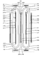
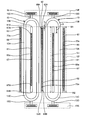
- FIG. 1 is a plan view schematically showing an electrode structure of a GaN-based HFET according to the first embodiment of the present invention.
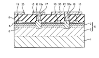
- FIG. 2 is a cross-sectional view taken along line BB in FIG.
- FIG. 3 is a view showing a cross section taken along line AA of FIG.
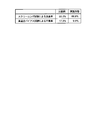
- FIG. 4 is a view showing a reliability test result between the first embodiment and the comparative GaN-based HFET.
- FIG. 5 is a plan view schematically showing the electrode structure of the GaN-based HFET of the comparative example.
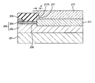
- 6 is a cross-sectional view taken along the line CC of FIG.
- FIG. 7 is a plan view schematically showing an electrode structure of a GaN-based HFET according to the second embodiment of the present invention.
- FIG. 1 is a plan view schematically showing an electrode structure of a GaN-based HFET according to the first embodiment of the present invention.
- FIG. 2 is a cross-sectional view taken along line BB in FIG.
- FIG. 3 is a view showing a cross section taken along line AA of FIG.
- an undoped GaN layer 2 and an undoped AlGaN layer 3 are formed on a Si substrate 1.
- the undoped GaN layer 2 and the undoped AlGaN layer 3 constitute a GaN-based stacked body 5 having a heterojunction.
- a channel layer is formed by generating 2DEG (two-dimensional electron gas) 6 at the interface between the undoped GaN layer 2 and the undoped AlGaN layer 3.
- a protective film 7 and an interlayer insulating film 8 are sequentially formed on the GaN-based laminate 5.
- This protective film 7 is made of SiN.
- the film thickness of the protective film 7 is 150 nm.
- SiO 2 is used as a material of the interlayer insulating film 8.
- a recess reaching the undoped GaN layer 2 through the protective film 7 and the interlayer insulating film 8 is formed in the GaN-based laminate 5, and a drain electrode 11 and a source electrode 12 are formed as ohmic electrodes in the recess. .
- the drain electrode 11 and the source electrode 12 are Ti / Al / TiN electrodes in which a Ti layer, an Al layer, and a TiN layer are sequentially stacked.
- the gate electrode 13 is a WN / W electrode in which a WN layer and a W layer are sequentially stacked, and is formed as a Schottky electrode that is in Schottky junction with the undoped AlGaN layer 3.
- the Schottky junction between the WN / W electrode and the undoped AlGaN layer 3 is used.
- a MISHFET Metal Insulator
- Semiconductor-Heterostructure-Field-Effect-Transistor Metal Insulator, Semiconductor, Heterojunction Field Effect Transistor).
- the interlayer insulating film 8 is formed so as to cover the drain electrode 11, the source electrode 12 and the gate electrode 13.
- a contact hole 17 is provided on a part of the drain electrode 11 of the interlayer insulating film 8.
- a contact hole 18 is provided on a partial region of the source electrode 12 of the interlayer insulating film 8.
- a drain wiring 15 is provided in the contact hole 17 and on the interlayer insulating film 8, and the drain wiring 15 is electrically connected to the drain electrode 11.
- the drain wiring 15 provided in the contact hole 17 forms the second contact portion 15a.
- a source wiring 20 is provided in the contact hole 18 and on the interlayer insulating film 8, and the source wiring 20 is electrically connected to the source electrode 12.
- a source wiring 20 provided in the contact hole 18 forms a first contact portion 20a.
- TiN / Al, Ti / Cu, Ti / Au, Ti / Al, or the like is used as the drain wiring 15 and the source wiring 20.
- this embodiment includes two finger-shaped drain electrodes 11 and three finger-shaped source electrodes 12.
- the two drain electrodes 11 are formed in parallel to each other.
- the three source electrodes 12 are formed in parallel to each other so as to be alternately arranged with the drain electrodes 11 in the arrangement direction of the drain electrodes 11.
- each source electrode 12 in the longitudinal direction is shorter than the length L1 of each drain electrode 11 in the longitudinal direction.
- each source electrode 12 is located between the end 11A in the longitudinal direction of each drain electrode 11 and the end 11B in the longitudinal direction.
- the first contact portion 20 a extends in the longitudinal direction of the source electrode 12.
- the length of the first contact portion 20a in the longitudinal direction is shorter than the length of the source electrode 12 in the longitudinal direction.
- the second contact portion 15 a extends in the longitudinal direction of the drain electrode 11.
- the length in the longitudinal direction of the second contact portion 15 a is shorter than the length in the longitudinal direction of the drain electrode 11.
- the gate electrode 13 includes a longitudinally extending portion 13A and curved portions 13B and 13C extending in the longitudinal direction of the drain electrode 11 between the finger-like drain electrode 11 and the finger-like source electrode 12 in plan view. And have.
- the curved portion 13B extends so as to surround the end 11A of the drain electrode 11 in a plan view, and is connected to one end of two longitudinally extending portions 13A adjacent to each other with the drain electrode 11 interposed therebetween. Further, the curved portion 13C extends so as to surround the end 11B of the drain electrode 11 in plan view, and continues to the other end of the two longitudinally extending portions 13A adjacent to each other with the drain electrode 11 interposed therebetween. .
- each longitudinally extending portion 13 ⁇ / b> A of the gate electrode 13 has a shorter distance from the source electrode 12 than the distance from the drain electrode 11 in the arrangement direction of the drain electrodes 11. Is located.
- the distance D2 between the drain electrode 11 and the longitudinal extension 13A of the gate electrode 13 in the arrangement direction, the ends 11A and 11B of the drain electrode 11 in the longitudinal direction of the drain electrode 11, and the curved portion of the gate electrode 13 is 1: 1.5.
- the distance X between the longitudinal ends 11A and 11B of the drain electrode 11 and the longitudinal ends 17A and 17B of the second contact portion 15a is equal to the longitudinal ends 12A and 12B of the source electrode 12 and the first contact. It is longer than the distance Y between the longitudinal ends 18A and 18B of the portion 20a.
- the GaN-based HFET configured as described above is a normally-on type, and is turned off by applying a negative voltage to the gate electrode 13.
- FIG. 4 shows the reliability test results of the GaN-based HFET of the first embodiment and the GaN-based HFET of the comparative example.
- FIG. 5 is a plan view schematically showing the electrode structure of the GaN-based HFET of the comparative example.
- the GaN-based HFET of the comparative example is an example for comparison and is not the present invention.
- the GaN-based HFET of the comparative example has a distance X ′ between the longitudinal end 211A of the drain electrode 211 and the longitudinal end 217A of the second contact portion 215a. Only the point equal to the distance Y between the longitudinal end 212A of 212 and the longitudinal end 218A of the first contact portion 220a is different from the first embodiment.
- the yield (non-defective product rate) according to the screening test of the GaN-based HFET of this comparative example was 66.2%.
- this screening test for example, 0 V is applied to the source electrode 212 and 600 V in increments of +100 V to the drain electrode 211 in an off state in which the application to the gate electrode 13 is continued at ⁇ 10 V. This is a test for observing whether destruction or characteristic deterioration occurs. In this screening test, a short circuit occurred between the source electrode 212 and the drain electrode 211.
- the defect rate by the high temperature reverse bias test of the above comparative example was 17.3%.
- this high temperature reverse bias test for example, 0 V is applied to the source electrode 212 and 600 V is applied to the drain electrode 211 in an off state in which the gate electrode 13 is continuously applied with ⁇ 10 V in a high temperature environment (200 ° C.).
- the device is continuously applied for 5 minutes to observe whether the device is broken or the device characteristics are deteriorated.
- the screening test was passed, a defect occurred in the high temperature reverse bias test with a high probability of a quarter.
- the cause of failure in the high temperature reverse bias test of the above comparative example is estimated as follows. That is, in the OFF state in which the voltage is continuously applied to the gate electrode 13, the ends 211A and 211B of the drain electrode 211 and the ends 217A and 217A of the second contact portion 215a are generated by an electric field when a high voltage of 600 V is applied to the drain electrode 211. The electric field concentrates on 217B. For this reason, current concentrates locally, acts on defects in the vicinity of the ends 211A and 211B of the drain electrode 211 and the ends 217A and 217B of the second contact portion 215a, and causes a failure in which the life deterioration is promoted and destroyed. I imagine that. That is, the cause of the failure due to the high temperature reverse bias test is assumed to be due to electric field concentration at the ends 211A and 211B of the drain electrode 211 and the ends 217A and 217B of the second contact portion 215a.
- the failure rate of the GaN-based HFET of this embodiment by the high temperature reverse bias test was 9.9%, which was improved by 7% or more compared to the failure rate of 17.3% in the comparative example.
- the screening test result of this embodiment was 68.8%, which was equivalent to the comparative example.
- the distance X between the ends 11A, 11B of the drain electrode 11 and the ends 17A, 17B of the second contact portion 15a is equal to the ends 12A, 12B of the source electrode 12 and the first contact portion. It is assumed that the electric field concentration at the ends 11A and 11B of the drain electrode 11 and the ends 17A and 17B of the second contact portion 15a can be alleviated by the configuration that is longer than the distance Y between the ends 18A and 18B of 20a.
- a plurality of finger-like drain electrodes 11 and source electrodes 12 are provided. Therefore, it is possible to remarkably suppress the occurrence of element destruction and deterioration at the ends 17A and 17B of the second contact portion 15a, and to improve the reliability.
- the source wiring 20 electrically connected via the first contact portion 20a is disposed on the source electrode 12. Therefore, the chip area can be reduced by such a three-dimensional structure.
- the gate electrode 13 extends so as to surround the ends 11A and 11B on both sides of the drain electrode 11 in the longitudinal direction. Therefore, the concentration of the electric field on the ends 11A and 11B of the drain electrode 11 can be suppressed during the off breakdown voltage test, and the static off breakdown voltage can be improved.
- FIG. 7 is a plan view schematically showing the electrode structure of the GaN-based HFET of the second embodiment.
- the distance X between the longitudinal ends 61A and 61B of the drain electrode 61 and the longitudinal ends 67A and 67B of the second contact portion 65a. Is longer than the distance Y between the longitudinal ends 62A, 62B of the source electrode 62 and the longitudinal ends 68A, 68B of the first contact portion 70a.
- virtual lines M1 and M2 extending from the longitudinal ends 62A and 62B of the source electrode 62 in the lateral direction perpendicular to the longitudinal direction are in contact with the ends 61A and 61B of the drain electrode 61. That is, the only difference from the first embodiment is that the positions of the ends 62A and 62B of the source electrode 62 in the longitudinal direction coincide with the positions of the ends 61A and 61B of the drain electrode 61, respectively.
- the high-temperature reverse bias test result of the GaN-based HFET of the second embodiment is improved to be equivalent to that of the GaN-based HFET of the first embodiment, which is higher than the failure rate of 17.3% of the comparative example shown in FIG. , Improved by more than 7%.
- the present embodiment as in the first embodiment, it is possible to remarkably suppress the occurrence of element destruction and deterioration at the ends 17A and 17B of the second contact portion 15a, thereby improving the reliability.
- two finger-shaped drain electrodes 11 and 61 are provided and three finger-shaped source electrodes 12 and 62 are provided.
- three finger-shaped drain electrodes are provided, Four finger-shaped source electrodes may be provided.
- the four source electrodes may be alternately arranged with the drain electrodes in the arrangement direction of the drain electrodes.
- one finger-shaped drain electrode may be provided, two finger-shaped source electrodes may be provided, four or more finger-shaped drain electrodes may be provided, and five or more finger-shaped source electrodes may be provided.
- the source electrode may be alternately arranged in the arrangement direction.
- the gate electrode 13 surrounds each finger-shaped drain electrode 11 in a ring shape, but the curved portion 13B may not be provided.
- each source electrode 12 is located between the end 11A in the longitudinal direction of each drain electrode 11 and the end 11B in the longitudinal direction. In the direction, it may not be located between both ends of the drain electrode in the longitudinal direction. Further, a part of the source electrode may be located between both ends of the drain electrode in the longitudinal direction. That is, only one end in the longitudinal direction of the source electrode may be located between both ends in the longitudinal direction of the drain electrode in the longitudinal direction.
- the substrate 1 is a Si substrate.
- the substrate 1 is not limited to a Si substrate, and a sapphire substrate or a SiC substrate may be used.
- a nitride semiconductor layer is grown on the sapphire substrate or the SiC substrate.
- a Ga-based semiconductor layer may be grown on a substrate made of a Ga-based semiconductor, such as by growing an AlGaN layer on a GaN substrate.
- a buffer layer may be appropriately formed between the substrate and each layer.
- a hetero improvement layer made of AlN may be formed between the undoped GaN layer and the undoped AlGaN layer.
- a GaN cap layer may be formed on the undoped AlGaN layer.
- the recess reaching the undoped GaN layer 2 is formed, and the drain electrodes 11 and 61 and the source electrodes 12 and 62 are formed as ohmic electrodes in the recess.
- the recess is formed.
- the drain electrode and the source electrode may be formed on the undoped AlGaN layer on the undoped GaN layer, and the drain electrode and the source electrode may be ohmic electrodes by reducing the thickness of the undoped AlGaN layer. Further, ion implantation may be performed so that the drain electrode and the source electrode are ohmic electrodes.
- the gate electrode 13 is made of WN / W, but may be made of TiN.
- the gate electrode may be made of Ti / Au or Ni / Au.
- the drain electrodes 11 and 61 and the source electrodes 12 and 62 are Ti / Al / TiN electrodes, but may be Ti / Al electrodes or Hf / Al electrodes.
- a Ti / AlCu / TiN electrode may be used.
- the drain electrode and the source electrode may be formed by stacking Ni / Au on Ti / Al or Hf / Al, or may be formed by stacking Pt / Au on Ti / Al or Hf / Al.
- Au may be laminated on Ti / Al or Hf / Al.
- the first contact portions 20a and 70a are part of the source wiring 20, but the first contact portion and the source wiring may be separated. Further, although the second contact portions 15a and 70a are part of the drain wiring 15, the second contact portion and the drain wiring may be separated.
- the protective film 7 is made of SiN.
- the protective film 7 may be made of SiO 2 , Al 2 O 3 or the like, and a laminated film in which a SiO 2 film is laminated on a SiN film. Also good.
- the thickness of the protective film 7 is 150 nm, but may be set in the range of 20 nm to 250 nm.
- the interlayer insulating film 8 is made of SiO 2.
- an insulating material such as SiN, SOG (Spin On Glass), BPSG (Boron Phosphorous Silicate Glass), or polyimide is used. Also good.
- the GaN-based stacked body 5 in the field effect transistor of the present invention includes a GaN-based semiconductor layer represented by Al X In Y Ga 1- XYN (X ⁇ 0, Y ⁇ 0, 0 ⁇ X + Y ⁇ 1). May be included. That is, the GaN-based laminate may include AlGaN, GaN, InGaN, or the like.
- the normally-on type HFET has been described.
- the normally-off type can achieve the same effect.
- the Schottky gate has been described, an insulated gate structure may be used.
- the heterojunction field effect transistor of the present invention is A GaN-based laminate 5 having a heterojunction; A plurality of drain electrodes 11, 61 formed in a finger shape on the GaN-based laminate 5 in parallel with each other; A plurality of source electrodes formed in parallel with each other in a finger shape on the GaN-based laminate 5 so as to be alternately arranged with the plurality of drain electrodes 11, 61 in the arrangement direction of the plurality of drain electrodes 11, 61.
- gate electrodes 13 formed between the drain electrodes 11 and 61 and the source electrodes 12 and 62, respectively;
- An interlayer insulating film 8 formed on the GaN-based laminate 5 so as to cover the source electrodes 12 and 62, the drain electrodes 11 and 61, and the gate electrode 13;
- First contact portions 20a, 70a formed on at least a part of the source electrodes 12, 62 and in the interlayer insulating film 8 and extending in the longitudinal direction of the source electrodes 12, 62;
- Second contact portions 15a and 65a formed on at least a part of the drain electrodes 11 and 61 and on the interlayer insulating film 8 and extending in the longitudinal direction of the drain electrodes 11 and 61;
- the length of the first contact portions 20a, 70a in the longitudinal direction is shorter than the length of the source electrodes 12, 62 in the longitudinal direction
- the length of the second contact portions 15a and 65a in the longitudinal direction is shorter than the length of the drain electrodes 11 and 61 in the longitudinal direction.
- each of the drain electrodes 11, 61 the ends 11A, 11B of the drain electrodes 11, 61 outside the second contact portions 15a, 65a from the ends 17A, 17B, 67A, 67B of the second contact portions 15a, 65a.
- the distance X to 61A, 61B is the end 12A, 12B of the source electrode 12, 62 outside the first contact portion 20a, 70a from the end 18A, 18B, 68A, 68B of the first contact portion 20a, 70a. It is characterized by being longer than each distance Y to 62A, 62B.
- the distance X between the ends 11A, 11B, 61A, 61B of the drain electrodes 11, 61 and the ends 17A, 17B, 67A, 67B of the second contact portions 15a, 65a is The distance Y between the ends 12A, 12B, 62A, 62B of the source electrodes 12, 62 and the ends 18A, 18B, 68A, 68B of the first contact portions 20a, 70a is longer. For this reason, when the high temperature reverse bias test is performed, the electric field concentration at the ends 17A, 17B, 67A, and 67B of the second contact portions 15a and 65a can be reduced.
- a plurality of finger-like drain electrodes 11 and 61 and source electrodes 12 and 62 are provided. Therefore, it is possible to remarkably suppress the occurrence of element destruction and deterioration at the ends 17A, 17B, 67A, and 67B of the second contact portions 15a and 65a, thereby improving the reliability.
- a source wiring 20 is formed on the interlayer insulating film 8 and electrically connected to the source electrodes 12 and 62 via the first contact portions 20a and 70a.
- the three-dimensional structure in which the source wiring 20 formed on the interlayer insulating film 8 and electrically connected to the source electrodes 12 and 62 via the first contact portions 20a and 70a is disposed.
- the chip area can be reduced.
- the gate electrode 13 extends in the longitudinal direction of the drain electrodes 11, 61 between the drain electrodes 11, 61 and the source electrodes 12, 62 in a plan view, and the drain electrodes 11, 61. It extends so as to surround the ends 11A, 11B, 61A, 61B on both sides in the longitudinal direction.
- the gate electrode 13 extends so as to surround the ends 11A, 11B, 61A, 61B on both sides in the longitudinal direction of the drain electrodes 11, 61. Concentration of the electric field on the ends 11A and 11B of the semiconductor device can be suppressed, and static off-breakdown voltage can be improved.
Landscapes
- Junction Field-Effect Transistors (AREA)
- Electrodes Of Semiconductors (AREA)
Abstract
Description
ヘテロ接合を有するGaN系積層体と、
上記GaN系積層体上にフィンガー状に互いに平行に形成された複数のドレイン電極と、
上記GaN系積層体上に、上記複数のドレイン電極の配列方向に上記複数のドレイン電極と交互に配列するようにフィンガー状に互いに平行に形成された複数のソース電極と、
平面視において、上記ドレイン電極と上記ソース電極との間にそれぞれ形成されたゲート電極と、
上記GaN系積層体上に、上記ソース電極、上記ドレイン電極、および上記ゲート電極を覆うように形成された層間絶縁膜と、
上記各ソース電極の少なくとも一部の領域上、かつ、上記層間絶縁膜に形成され、上記ソース電極の長手方向に延在している第1コンタクト部と、
上記各ドレイン電極の少なくとも一部の領域上、かつ、上記層間絶縁膜に形成され、上記ドレイン電極の長手方向に延在している第2コンタクト部と、
を備え、
上記第1コンタクト部の長手方向の長さは、上記ソース電極の長手方向の長さよりも短く、
上記第2コンタクト部の長手方向の長さは、上記ドレイン電極の長手方向の長さよりも短く、
上記各ドレイン電極において、上記第2コンタクト部の端から上記第2コンタクト部より外側の上記ドレイン電極の端までの距離は、上記第1コンタクト部の端から上記第1コンタクト部より外側の上記ソース電極の端までの距離よりも長いことを特徴としている。
上記層間絶縁膜上に形成され、上記ソース電極に上記第1コンタクト部を介して電気的に接続されたソース配線を備えている。
上記ゲート電極は、平面視において、上記ドレイン電極と上記ソース電極との間で上記ドレイン電極の長手方向に延在していると共に、上記ドレイン電極の長手方向の両側の端部を囲むように延在している。
図1は、本発明の第1実施形態であるGaN系のHFETの電極構造を模式的に示す平面図である。また、図2は、図1のB-B線断面を示す図である。また、図3は、図1のA-A線断面を示す図である。
次に、本発明の第2実施形態のGaN系のHFETを説明する。
ヘテロ接合を有するGaN系積層体5と、
上記GaN系積層体5上にフィンガー状に互いに平行に形成された複数のドレイン電極11,61と、
上記GaN系積層体5上に、上記複数のドレイン電極11,61の配列方向に上記複数のドレイン電極11,61と交互に配列するように、フィンガー状に互いに平行に形成された複数のソース電極12,62と、
平面視において、上記ドレイン電極11,61と上記ソース電極12,62との間にそれぞれ形成されたゲート電極13と、
上記GaN系積層体5上に、上記ソース電極12,62、上記ドレイン電極11,61、および上記ゲート電極13を覆うように形成された層間絶縁膜8と、
上記各ソース電極12,62の少なくとも一部の領域上、かつ、上記層間絶縁膜8に形成され、上記ソース電極12,62の長手方向に延在している第1コンタクト部20a,70aと、
上記各ドレイン電極11,61の少なくとも一部の領域上、かつ、上記層間絶縁膜8に形成され、上記ドレイン電極11,61の長手方向に延在している第2コンタクト部15a,65aと、
を備え、
上記第1コンタクト部20a,70aの長手方向の長さは、上記ソース電極12,62の長手方向の長さよりも短く、
上記第2コンタクト部15a,65aの長手方向の長さは、上記ドレイン電極11,61の長手方向の長さよりも短く、
上記各ドレイン電極11,61において、上記第2コンタクト部15a,65aの端17A,17B,67A,67Bから上記第2コンタクト部15a,65aより外側の上記ドレイン電極11,61の端11A,11B,61A,61Bまでの距離Xは、上記第1コンタクト部20a,70aの端18A,18B,68A,68Bから上記第1コンタクト部20a,70aより外側の上記ソース電極12,62の端12A,12B,62A,62Bまでのそれぞれの距離Yよりも長いことを特徴としている。
上記層間絶縁膜8上に形成され、上記ソース電極12,62に上記第1コンタクト部20a,70aを介して電気的に接続されたソース配線20を備える。
上記ゲート電極13は、平面視において、上記ドレイン電極11,61と上記ソース電極12,62との間で上記ドレイン電極11,61の長手方向に延在していると共に、上記ドレイン電極11,61の長手方向の両側の端11A,11B,61A,61Bを囲むように延在している。
2 アンドープGaN層
3 アンドープAlGaN層
5 GaN系積層体
6 2DEG(2次元電子ガス)
7 保護膜
8 層間絶縁膜
11,61 ドレイン電極
11A,11B,61A,61B 端
12,62 ソース電極
12A,12B,62A,62B 端
13 ゲート電極
13A 長手方向延在部
13B,13C 湾曲部
13D 枝部
13E 連接部
15 ドレイン配線
15a,65a 第2コンタクト部
17,18,19 コンタクトホール
17A,17B,67A,67B 端
18A,18B,68A,68B 端
20 ソース配線
20a,70a 第1コンタクト部
X,Y 距離
Claims (3)
- ヘテロ接合を有するGaN系積層体(5)と、
上記GaN系積層体(5)上にフィンガー状に互いに平行に形成された複数のドレイン電極(11,61)と、
上記GaN系積層体(5)上に、上記複数のドレイン電極(11,61)の配列方向に上記複数のドレイン電極(11,61)と交互に配列するように、フィンガー状に互いに平行に形成された複数のソース電極(12,62)と、
平面視において、上記ドレイン電極(11,61)と上記ソース電極(12,62)との間にそれぞれ形成されたゲート電極(13)と、
上記GaN系積層体(5)上に、上記ソース電極(12,62)、上記ドレイン電極(11,61)、および上記ゲート電極(13)を覆うように形成された層間絶縁膜(8)と、
上記各ソース電極(12,62)の少なくとも一部の領域上、かつ、上記層間絶縁膜(8)に形成され、上記ソース電極(12,62)の長手方向に延在している第1コンタクト部(20a,70a)と、
上記各ドレイン電極(11,61)の少なくとも一部の領域上、かつ、上記層間絶縁膜(8)に形成され、上記ドレイン電極(11,61)の長手方向に延在している第2コンタクト部(15a,65a)と、
を備え、
上記第1コンタクト部(20a,70a)の長手方向の長さは、上記ソース電極(12,62)の長手方向の長さよりも短く、
上記第2コンタクト部(15a,65a)の長手方向の長さは、上記ドレイン電極(11,61)の長手方向の長さよりも短く、
上記各ドレイン電極(11,61)において、上記第2コンタクト部(15a,65a)の端(17A,17B,67A,67B)から上記第2コンタクト部(15a,65a)より外側の上記ドレイン電極(11,61)の端(11A,11B,61A,61B)までの距離Xは、上記第1コンタクト部(20a,70a)の端(18A,18B,68A,68B)から上記第1コンタクト部(20a,70a)より外側の上記ソース電極(12,62)の端(12A,12B,62A,62B)までのそれぞれの距離Yよりも長いことを特徴とするヘテロ接合電界効果トランジスタ。 - 請求項1に記載のヘテロ接合電界効果トランジスタにおいて、
上記層間絶縁膜(8)上に形成され、上記ソース電極(12,62)に上記第1コンタクト部(20a,70a)を介して電気的に接続されたソース配線(20)を備えることを特徴とするヘテロ接合電界効果トランジスタ。 - 請求項1または2に記載のヘテロ接合電界効果トランジスタにおいて、
上記ゲート電極(13)は、
平面視において、上記ドレイン電極(11,61)と上記ソース電極(12,62)との間で上記ドレイン電極(11,61)の長手方向に延在していると共に、上記ドレイン電極(11,61)の長手方向の両側の端(11A,11B,61A,61B)を囲むように延在していることを特徴とするヘテロ接合電界効果トランジスタ。
Priority Applications (3)
| Application Number | Priority Date | Filing Date | Title |
|---|---|---|---|
| CN201480030382.0A CN105264650B (zh) | 2013-06-13 | 2014-02-28 | 异质结场效应晶体管 |
| JP2015522580A JP5948500B2 (ja) | 2013-06-13 | 2014-02-28 | ヘテロ接合電界効果トランジスタ |
| US14/785,504 US9461158B2 (en) | 2013-06-13 | 2014-02-28 | Heterojunction field effect transistor |
Applications Claiming Priority (2)
| Application Number | Priority Date | Filing Date | Title |
|---|---|---|---|
| JP2013124546 | 2013-06-13 | ||
| JP2013-124546 | 2013-06-13 |
Publications (1)
| Publication Number | Publication Date |
|---|---|
| WO2014199671A1 true WO2014199671A1 (ja) | 2014-12-18 |
Family
ID=52021978
Family Applications (1)
| Application Number | Title | Priority Date | Filing Date |
|---|---|---|---|
| PCT/JP2014/055016 Ceased WO2014199671A1 (ja) | 2013-06-13 | 2014-02-28 | ヘテロ接合電界効果トランジスタ |
Country Status (4)
| Country | Link |
|---|---|
| US (1) | US9461158B2 (ja) |
| JP (1) | JP5948500B2 (ja) |
| CN (1) | CN105264650B (ja) |
| WO (1) | WO2014199671A1 (ja) |
Cited By (3)
| Publication number | Priority date | Publication date | Assignee | Title |
|---|---|---|---|---|
| JP2018142664A (ja) * | 2017-02-28 | 2018-09-13 | パナソニックIpマネジメント株式会社 | 窒化物半導体装置 |
| US10545055B2 (en) | 2017-06-13 | 2020-01-28 | Semiconductor Components Industries, Llc | Electronic device including a temperature sensor |
| WO2026069411A1 (ja) * | 2024-09-24 | 2026-04-02 | 株式会社 東芝 | 半導体装置 |
Families Citing this family (5)
| Publication number | Priority date | Publication date | Assignee | Title |
|---|---|---|---|---|
| US9882041B1 (en) * | 2016-11-17 | 2018-01-30 | Texas Instruments Incorporated | HEMT having conduction barrier between drain fingertip and source |
| JP6812764B2 (ja) * | 2016-11-29 | 2021-01-13 | 日亜化学工業株式会社 | 電界効果トランジスタ |
| DE102020112069B4 (de) | 2020-02-27 | 2022-03-03 | Taiwan Semiconductor Manufacturing Co. Ltd. | Source-leckstromunterdrückung durch source-umgebende gate-struktur und verfahren zur herstellung der gate-struktur |
| US11791388B2 (en) * | 2020-02-27 | 2023-10-17 | Taiwan Semiconductor Manufacturing Company, Ltd. | Source leakage current suppression by source surrounding gate structure |
| US12112983B2 (en) | 2020-08-26 | 2024-10-08 | Macom Technology Solutions Holdings, Inc. | Atomic layer deposition of barrier metal layer for electrode of gallium nitride material device |
Citations (4)
| Publication number | Priority date | Publication date | Assignee | Title |
|---|---|---|---|---|
| JP2012018961A (ja) * | 2010-07-06 | 2012-01-26 | Sanken Electric Co Ltd | 半導体装置 |
| JP2012023210A (ja) * | 2010-07-14 | 2012-02-02 | Sumitomo Electric Ind Ltd | 半導体装置 |
| JP2012238808A (ja) * | 2011-05-13 | 2012-12-06 | Sharp Corp | 電界効果トランジスタ |
| JP2012248588A (ja) * | 2011-05-26 | 2012-12-13 | Renesas Electronics Corp | 半導体装置 |
Family Cites Families (10)
| Publication number | Priority date | Publication date | Assignee | Title |
|---|---|---|---|---|
| US7465997B2 (en) * | 2004-02-12 | 2008-12-16 | International Rectifier Corporation | III-nitride bidirectional switch |
| JP2007294769A (ja) * | 2006-04-26 | 2007-11-08 | Toshiba Corp | 窒化物半導体素子 |
| JP2010147349A (ja) | 2008-12-19 | 2010-07-01 | Advantest Corp | 半導体装置、半導体装置の製造方法およびスイッチ回路 |
| JP4985760B2 (ja) * | 2009-12-28 | 2012-07-25 | 住友電気工業株式会社 | 半導体装置およびその製造方法 |
| US8319256B2 (en) * | 2010-06-23 | 2012-11-27 | Power Integrations, Inc. | Layout design for a high power, GaN-based FET |
| JP5457292B2 (ja) * | 2010-07-12 | 2014-04-02 | パナソニック株式会社 | 窒化物半導体装置 |
| CN103229284B (zh) * | 2010-10-01 | 2016-05-25 | 夏普株式会社 | 氮化物半导体装置 |
| US9379231B2 (en) * | 2012-02-17 | 2016-06-28 | Infineon Technologies Americas Corp. | Transistor having increased breakdown voltage |
| JP5985282B2 (ja) * | 2012-07-12 | 2016-09-06 | ルネサスエレクトロニクス株式会社 | 半導体装置 |
| WO2014174550A1 (ja) * | 2013-04-23 | 2014-10-30 | パナソニックIpマネジメント株式会社 | 窒化物半導体装置 |
-
2014
- 2014-02-28 JP JP2015522580A patent/JP5948500B2/ja active Active
- 2014-02-28 WO PCT/JP2014/055016 patent/WO2014199671A1/ja not_active Ceased
- 2014-02-28 CN CN201480030382.0A patent/CN105264650B/zh active Active
- 2014-02-28 US US14/785,504 patent/US9461158B2/en active Active
Patent Citations (4)
| Publication number | Priority date | Publication date | Assignee | Title |
|---|---|---|---|---|
| JP2012018961A (ja) * | 2010-07-06 | 2012-01-26 | Sanken Electric Co Ltd | 半導体装置 |
| JP2012023210A (ja) * | 2010-07-14 | 2012-02-02 | Sumitomo Electric Ind Ltd | 半導体装置 |
| JP2012238808A (ja) * | 2011-05-13 | 2012-12-06 | Sharp Corp | 電界効果トランジスタ |
| JP2012248588A (ja) * | 2011-05-26 | 2012-12-13 | Renesas Electronics Corp | 半導体装置 |
Cited By (3)
| Publication number | Priority date | Publication date | Assignee | Title |
|---|---|---|---|---|
| JP2018142664A (ja) * | 2017-02-28 | 2018-09-13 | パナソニックIpマネジメント株式会社 | 窒化物半導体装置 |
| US10545055B2 (en) | 2017-06-13 | 2020-01-28 | Semiconductor Components Industries, Llc | Electronic device including a temperature sensor |
| WO2026069411A1 (ja) * | 2024-09-24 | 2026-04-02 | 株式会社 東芝 | 半導体装置 |
Also Published As
| Publication number | Publication date |
|---|---|
| US9461158B2 (en) | 2016-10-04 |
| JPWO2014199671A1 (ja) | 2017-02-23 |
| CN105264650B (zh) | 2017-10-31 |
| JP5948500B2 (ja) | 2016-07-06 |
| US20160079404A1 (en) | 2016-03-17 |
| CN105264650A (zh) | 2016-01-20 |
Similar Documents
| Publication | Publication Date | Title |
|---|---|---|
| US11699751B2 (en) | Semiconductor device | |
| JP5948500B2 (ja) | ヘテロ接合電界効果トランジスタ | |
| JP5649347B2 (ja) | 半導体装置 | |
| US9754932B2 (en) | Semiconductor device | |
| JP6133191B2 (ja) | 窒化物半導体装置、ダイオード、および電界効果トランジスタ | |
| JP5712516B2 (ja) | 半導体装置 | |
| US20170352753A1 (en) | Field-effect transistor | |
| US20170345920A1 (en) | Field-effect transistor | |
| JP2016139718A (ja) | 半導体装置 | |
| TWI626742B (zh) | 半導體裝置 | |
| JP6272557B2 (ja) | 窒化物半導体電界効果トランジスタ | |
| JP6584987B2 (ja) | 半導体装置 | |
| WO2012157480A1 (ja) | 電界効果トランジスタ | |
| JP5629736B2 (ja) | 電界効果トランジスタ | |
| WO2012144100A1 (ja) | 窒化物系半導体装置 | |
| JP2015038935A (ja) | 窒化物半導体装置 | |
| US20150171203A1 (en) | Field-effect transistor | |
| JP2011142182A (ja) | 電界効果トランジスタ | |
| CN106373996A (zh) | 半导体装置 | |
| WO2023157452A1 (ja) | 窒化物半導体装置 | |
| WO2016151905A1 (ja) | 窒化物半導体装置 | |
| JP2013021361A (ja) | 電界効果トランジスタ | |
| JP2015002330A (ja) | 窒化物半導体装置 |
Legal Events
| Date | Code | Title | Description |
|---|---|---|---|
| WWE | Wipo information: entry into national phase |
Ref document number: 201480030382.0 Country of ref document: CN |
|
| 121 | Ep: the epo has been informed by wipo that ep was designated in this application |
Ref document number: 14810843 Country of ref document: EP Kind code of ref document: A1 |
|
| ENP | Entry into the national phase |
Ref document number: 2015522580 Country of ref document: JP Kind code of ref document: A |
|
| WWE | Wipo information: entry into national phase |
Ref document number: 14785504 Country of ref document: US |
|
| NENP | Non-entry into the national phase |
Ref country code: DE |
|
| 122 | Ep: pct application non-entry in european phase |
Ref document number: 14810843 Country of ref document: EP Kind code of ref document: A1 |