WO2014199639A1 - コンデンサ - Google Patents
コンデンサ Download PDFInfo
- Publication number
- WO2014199639A1 WO2014199639A1 PCT/JP2014/003128 JP2014003128W WO2014199639A1 WO 2014199639 A1 WO2014199639 A1 WO 2014199639A1 JP 2014003128 W JP2014003128 W JP 2014003128W WO 2014199639 A1 WO2014199639 A1 WO 2014199639A1
- Authority
- WO
- WIPO (PCT)
- Prior art keywords
- electrolyte
- capacitor
- sealing plate
- current collector
- blocking
- Prior art date
Links
Images


Classifications
-
- H—ELECTRICITY
- H01—ELECTRIC ELEMENTS
- H01G—CAPACITORS; CAPACITORS, RECTIFIERS, DETECTORS, SWITCHING DEVICES OR LIGHT-SENSITIVE DEVICES, OF THE ELECTROLYTIC TYPE
- H01G11/00—Hybrid capacitors, i.e. capacitors having different positive and negative electrodes; Electric double-layer [EDL] capacitors; Processes for the manufacture thereof or of parts thereof
- H01G11/78—Cases; Housings; Encapsulations; Mountings
- H01G11/80—Gaskets; Sealings
-
- H—ELECTRICITY
- H01—ELECTRIC ELEMENTS
- H01G—CAPACITORS; CAPACITORS, RECTIFIERS, DETECTORS, SWITCHING DEVICES OR LIGHT-SENSITIVE DEVICES, OF THE ELECTROLYTIC TYPE
- H01G11/00—Hybrid capacitors, i.e. capacitors having different positive and negative electrodes; Electric double-layer [EDL] capacitors; Processes for the manufacture thereof or of parts thereof
- H01G11/14—Arrangements or processes for adjusting or protecting hybrid or EDL capacitors
- H01G11/18—Arrangements or processes for adjusting or protecting hybrid or EDL capacitors against thermal overloads, e.g. heating, cooling or ventilating
-
- H—ELECTRICITY
- H01—ELECTRIC ELEMENTS
- H01G—CAPACITORS; CAPACITORS, RECTIFIERS, DETECTORS, SWITCHING DEVICES OR LIGHT-SENSITIVE DEVICES, OF THE ELECTROLYTIC TYPE
- H01G11/00—Hybrid capacitors, i.e. capacitors having different positive and negative electrodes; Electric double-layer [EDL] capacitors; Processes for the manufacture thereof or of parts thereof
- H01G11/22—Electrodes
- H01G11/24—Electrodes characterised by structural features of the materials making up or comprised in the electrodes, e.g. form, surface area or porosity; characterised by the structural features of powders or particles used therefor
-
- H—ELECTRICITY
- H01—ELECTRIC ELEMENTS
- H01G—CAPACITORS; CAPACITORS, RECTIFIERS, DETECTORS, SWITCHING DEVICES OR LIGHT-SENSITIVE DEVICES, OF THE ELECTROLYTIC TYPE
- H01G11/00—Hybrid capacitors, i.e. capacitors having different positive and negative electrodes; Electric double-layer [EDL] capacitors; Processes for the manufacture thereof or of parts thereof
- H01G11/66—Current collectors
-
- H—ELECTRICITY
- H01—ELECTRIC ELEMENTS
- H01G—CAPACITORS; CAPACITORS, RECTIFIERS, DETECTORS, SWITCHING DEVICES OR LIGHT-SENSITIVE DEVICES, OF THE ELECTROLYTIC TYPE
- H01G11/00—Hybrid capacitors, i.e. capacitors having different positive and negative electrodes; Electric double-layer [EDL] capacitors; Processes for the manufacture thereof or of parts thereof
- H01G11/74—Terminals, e.g. extensions of current collectors
-
- H—ELECTRICITY
- H01—ELECTRIC ELEMENTS
- H01G—CAPACITORS; CAPACITORS, RECTIFIERS, DETECTORS, SWITCHING DEVICES OR LIGHT-SENSITIVE DEVICES, OF THE ELECTROLYTIC TYPE
- H01G9/00—Electrolytic capacitors, rectifiers, detectors, switching devices, light-sensitive or temperature-sensitive devices; Processes of their manufacture
- H01G9/004—Details
- H01G9/08—Housing; Encapsulation
- H01G9/12—Vents or other means allowing expansion
-
- Y—GENERAL TAGGING OF NEW TECHNOLOGICAL DEVELOPMENTS; GENERAL TAGGING OF CROSS-SECTIONAL TECHNOLOGIES SPANNING OVER SEVERAL SECTIONS OF THE IPC; TECHNICAL SUBJECTS COVERED BY FORMER USPC CROSS-REFERENCE ART COLLECTIONS [XRACs] AND DIGESTS
- Y02—TECHNOLOGIES OR APPLICATIONS FOR MITIGATION OR ADAPTATION AGAINST CLIMATE CHANGE
- Y02E—REDUCTION OF GREENHOUSE GAS [GHG] EMISSIONS, RELATED TO ENERGY GENERATION, TRANSMISSION OR DISTRIBUTION
- Y02E60/00—Enabling technologies; Technologies with a potential or indirect contribution to GHG emissions mitigation
- Y02E60/13—Energy storage using capacitors
Definitions
- the technology of the present disclosure relates to capacitors such as electric double layer capacitors and electrolytic capacitors.
- the electrolyte impregnated in the capacitor element stays in the case.
- a capacitor is provided with a gas release mechanism.
- This gas release mechanism discharges the gas accumulated in the outer case when the capacitor is driven.
- a safety valve having gas permeability is used for this gas release mechanism.
- Patent Document 2 When the cap of the resin case is fused to the lower case by ultrasonic waves, the electrolyte flowing out of the polarizable electrode due to vibration is blocked by a blocking wall provided on the cap side to prevent contamination of the fused portion by the electrolyte. It is known (for example, Patent Document 2).
- a capacitor having a gas release mechanism such as a safety valve on the sealing plate is usually mounted with the sealing plate side up.
- a gas release mechanism such as a safety valve on the sealing plate
- a predetermined amount of electrolyte may be enclosed in the outer case to extend the life of the capacitor.
- the electrolyte sealed in the outer case flows inside the capacitor.
- the gas permeation path is blocked by the electrolyte. If the electrolyte adheres to the valve function part, the gas pressure cannot be directly applied to the valve function part. If the valve function part is covered with the electrolyte, the valve function is deteriorated, for example, the gas permeability is deteriorated, and the explosion-proof function is impaired, for example, the valve opening is delayed with respect to the rapid pressure increase.
- Patent Document 1 and Patent Document 2 have no disclosure or suggestion, and there is no disclosure or suggestion about a configuration or the like for solving the request or problem.
- an object of the present invention is to prevent a decrease in gas discharge function due to adhesion of a flowing electrolyte.
- a capacitor comprising an electrode overhang formed on an end surface and a current collector plate installed between the external terminals, a gas release mechanism installed on the sealing plate for releasing the gas in the exterior case; And a blocking mechanism that is installed on at least one of the sealing plate and the current collecting plate and blocks the electrolyte with respect to the gas release mechanism.
- the blocking mechanism includes a first blocking wall that stands on the sealing plate and blocks the electrolyte, and a second blocking wall that stands on the current collector and blocks the electrolyte.
- the second blocking wall may be provided at a different position with respect to the first blocking wall.
- the electrode projecting portion is formed by projecting an anode-side electrode body and a cathode-side electrode body at different positions on one surface portion of the element end surface, and the anode-side electrode body is formed.
- the electrode overhanging portion may include the current collector plate on the anode side, and the electrode overhang portion on the cathode side may include the current collector plate on the cathode side.
- an insulating interval is provided between the current collector plate on the anode side and the current collector plate on the cathode side, and a third barrier wall for blocking the electrolyte is provided in the insulating interval. May be.
- an insulating interval may be provided at a position facing the gas release mechanism.
- an electrolyte absorbing material that absorbs the electrolyte and blocks the electrolyte with respect to the gas release mechanism may be provided.
- the electrolyte absorbing material may be disposed within an insulating interval formed between the current collector plate on the anode side and the current collector plate on the cathode side.
- the electrolyte absorber includes an edge of the current collector plate on the anode side and the second barrier wall, and an edge of the current collector plate on the cathode side and the second barrier wall. It may be sandwiched between and fixed.
- the electrolyte absorber may be sandwiched and fixed between the element end surface and / or the end surface of the current collector plate and the sealing plate.
- the electrolyte that has been bounced up due to vibration of the soot capacitor is shut off by the shut-off mechanism, so that the discharge function of the gas release mechanism is not deteriorated.
- the capacitor of the present invention includes a blocking mechanism 6 for the electrolytic solution 4 in order to prevent a decrease in gas discharge function due to the flow of the electrolytic solution 4 contained in an electric double layer capacitor (hereinafter simply referred to as “capacitor”) 2.
- the electrolytic solution 4 is an example of an electrolyte having fluidity.
- the blocking mechanism 6 In the first embodiment, an example of the blocking mechanism 6 will be described.
- the first or second electrolytic solution absorbers 8-1 and 8-2 are included. If you have said.
- the electrolytic solution absorbers 8-1 and 8-2 are examples of the electrolyte absorber.
- an installation state of the electrolytic solution absorbers 8-1, 8-2 is described.
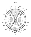
- FIG. 1 shows an example of a current collector plate and a capacitor element of the capacitor 2.
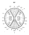
- FIG. 2 shows an example of the sealing plate.
- FIG. 3 shows a blocking mechanism 6 for the sealing plate and the current collecting plate.
- FIG. 4 shows a sealing part and a current collecting part of the capacitor 2.
- FIG. 5 shows the arrangement of the capacitor 2 and the electrolyte cutoff function.
- the capacitor 2 includes a capacitor element 10, an outer case 12, a sealing plate 14, and current collecting plates 18-1 and 18-2.
- the capacitor element 10 is impregnated with the electrolytic solution 4.
- the outer case 12 houses the electrolytic solution 4, the capacitor element 10, and current collector plates 18-1 and 18-2 and is sealed with a sealing plate 14.
- the electrolytic solution 4 is an example of an electrolyte and has fluidity.
- the sealing plate 14 is provided with a safety valve 16, and this safety valve 16 is an example of a gas vent valve and also an example of a gas release mechanism.
- the sealing plate 14 includes first blocking walls 6-11, 6-12, 6-13, 6-14, and the current collecting plates 18-1, 18-2 include second blocking walls 6-21, 6-22 is provided.
- the sealing plate 14 is provided with a third blocking wall 6-30.
- the blocking walls 6-11, 6-12, 6-13, 6-14, 6-21, 6-22 and 6-30 are examples of the blocking mechanism 6 that blocks the electrolyte solution 4 from the safety valve 16.
- FIG. 1A shows a part of the capacitor element 10.
- the capacitor element 10 is a winding element in which each of anode-side and cathode-side electrode foils and a separator 48 are overlapped and wound. This winding element is fixed by a fixing tape 50.
- a fixing tape 50 For example, an aluminum foil is used as a base material for the electrode foil, and polarizable electrodes including an active material such as activated carbon and a binder are formed on both surfaces of the aluminum foil.
- the capacitor element 10 has an element end face 52 formed by the edge of the separator 48.
- This element end face 52 is formed with anode-side and cathode-side electrode protruding portions 46-1 and 46-2 by drawing out the edge portions of the anode-side and cathode-side electrode foils.
- Each of the electrode overhang portions 46-1 and 46-2 is composed of a base member that exposes an aluminum surface on which no polarizable electrode is formed, and is formed by an edge portion of each electrode foil.
- each electrode overhanging portion 46-1 and 46-2 is formed in a fan shape having an angle of 120 degrees. For example, a cut is made in an arc portion having an angle of 40 degrees, It is flattened by bending to the side.
- an insulating interval is formed on the side of the opposing surface between the anode-side electrode overhanging portion 46-1 and the cathode-side electrode overhanging portion 46-2.
- This insulating interval includes a circular center portion formed at the center portion of the element end face 52 of the capacitor element 10.
- the current collector 18-1 shows the current collector 18-1 on the anode side.
- the current collector 18-1 is connected to the external terminal 24-1 on the anode side.
- the cathode side current collector 18-2 is similar to the current collector 18-1, and is connected to the cathode side external terminal 24-2.
- the current collector 18-1 includes a main body 32.
- the main body portion 32 is provided with linear edge portions 34 and 36 in the crossing direction, and includes a large-diameter arc portion 38 connecting the respective edge portions 34 and 36 and a small-diameter arc portion 40.
- the arc portion 38 is disposed on the peripheral side of the capacitor element 10, and the arc portion 40 is disposed near the center of the capacitor element 10.
- a triangular convex portion 70 is formed with one of its apexes facing the arc portion 40 of the current collector 18-1.
- One side of the convex portion 70 on the arc portion 38 side is a current collector connection surface portion 71 connected to the terminal connection surface portion 22 of the external terminal 24-1.
- each edge 34, 36 of the current collecting plate 18-1 second blocking walls 6-21, 6-22 for blocking the electrolyte solution 4 are installed.
- Each of the blocking walls 6-21 and 6-22 is formed of, for example, a rectangular flat plate.
- the second blocking walls 6-21 and 6-22 are arranged so that the main body 32 and the back surface of the sealing plate 14 (opposite surface of the capacitor element 10) when the current collector plate 18-1 and the external terminal 24-1 are connected. Is set to be equal to or lower than the height of the gap formed between the two.
- the cathode-side current collector 18-2 has the same shape as the anode-side current collector 18-1.
- FIG. 2 shows the back surface of the sealing plate (opposite surface of the capacitor element).
- This sealing plate 14 is an example of the sealing plate of the present invention.
- the sealing plate 14 is formed of, for example, a hard insulating synthetic resin.
- the sealing plate 14 includes an anode-side external terminal 24-1, a cathode-side external terminal 24-2, a safety valve 16 serving as a gas release mechanism, and a plurality of first shut-offs that shut off the electrolyte solution 4 (B in FIG. 5).
- Walls 6-11, 6-12, 6-13, 6-14 and a third blocking wall 6-30 are formed.
- the first barrier walls 6-11, 6-12, 6-13, 6-14 are connected to the current collector plates 18-1, 18-2 and the external terminals 24-1, 24-2.
- the third blocking wall 6-30 is formed at a portion facing the insulating interval formed between the current collecting plates 18-1 and 18-2, and the first blocking walls 6-11 and 6-12 are formed. , 6-13, and 6-14. That is, the current collecting plates 18-1 and 18-2 do not exist on the facing surface of the third blocking wall 6-30.
- Each of the external terminals 24-1 and 24-2 is formed of a metal material having good conductivity, and is attached to the sealing plate 14 by insert molding.
- a terminal connection surface portion 22 is formed on each of the external terminals 24-1 and 24-2.
- the anode-side current collector 18-1 is connected to the terminal connection surface 22 of the external terminal 24-1, and the cathode-side current collector 18-2 is connected to the terminal connection surface 22 of the external terminal 24-2. .
- the safety valve 16 is installed in a valve hole portion 26 provided in the sealing plate 14.
- the safety valve 16 is provided with a gas permeable membrane portion, and this membrane portion is installed in the valve hole portion 26.
- the third blocking wall 6-30 is installed in the vicinity of the center O of the sealing plate 14.
- the third blocking wall 6-30 is, for example, a triangular prism that is erected in a direction perpendicular to the back surface of the sealing plate 14.
- the third blocking wall 6-30 includes a surface portion 28 parallel to the edge of the current collecting plate 18-1 or the current collecting plate 18-2, and a surface portion 30 intersecting the surface portion 28.
- Each of the first blocking walls 6-11, 6-12, 6-13, 6-14 is a rectangular parallelepiped as an example.
- Each of the blocking walls 6-11, 6-12, 6-13, 6-14 is arranged in parallel with the edge of the current collector plate 18-1 or the current collector plate 18-2.
- the current collecting plates 18-1 and 18-2 are arranged symmetrically with the center O of the sealing plate 14, the safety valve 16 and the third blocking wall 6-30 interposed therebetween.
- the electrode projecting portions 46-1 and 46-2 formed on the element end face 52 of the capacitor element 10 and the current collector plates 18-1 and 18-2 are connected.
- the anode-side current collector 18-1 is used as the electrode overhanging portion 46-1
- the cathode-side current collector 18-2 is used as the electrode overhanging portion 46-2
- the surfaces on which the convex portions 70 are not formed are electrodes. Place on the overhanging portions 46-1 and 46-2. At this time, the current collecting plates 18-1 and 18-2 are placed with the arc portion 40 aligned with the center of the element, and the current collecting plate 18-1 and the current collecting plate 18-2 are not in contact with each other. .
- the portion of the main body 32 where the convex portion 70 is not formed is irradiated with laser from the current collecting plates 18-1 and 18-2 side, and the current collecting plates 18-1 and 18-2 and the electrode overhanging portion 46 are irradiated. -1, 46-2 are welded.
- the capacitor element 10 is shielded by using an inert gas such as argon gas or helium gas as a shielding gas, and the influence of laser heat or sputtering on the capacitor element 10 is avoided.
- the current collector plates 18-1 and 18-2 connected to the capacitor element 10 and the external terminals 24-1 and 24-2 formed on the sealing plate 14 are connected.
- the terminal connection surface portions 22 of the external terminals 24-1 and 24-2 are placed so as to be connected to the current collector plate connection surface portion 71 of the convex portion 70 formed on the main body portion 32 of the current collector plates 18-1 and 18-2.
- the terminal connection surface portion 22 and the current collector plate connection surface portion 71 are irradiated with laser from the arc portion 38 side of the current collector plates 18-1 and 18-2 around the grounding portion of the current collector plate connection surface portion 71 and the current collector plate connection surface portion 71. 71 is connected.
- the main body portion 32 is disposed between the current collector plate connection surface portion 71 and the circular arc portion 38, it is possible to prevent spatter generated by laser irradiation from falling on the element end surface 52 of the capacitor element 10 and to prevent a short circuit. To avoid.
- FIG. 3 shows a sealing plate 14 having current collecting plates 18-1 and 18-2 connected to external terminals 24-1 and 24-2.
- a space portion 54 (FIG. 4) corresponding to the protruding length of 1,4-2 is formed.
- the space part 54 or a space formed by the insulating interval between the current collector 18-1 and the current collector 18-2 is a space that can serve as a movement path of the electrolyte 4 when the electrolyte 4 jumps up.
- the first blocking walls 6-11, 6-12, 6-13, 6-14 and the third blocking wall 6-30 on the sealing plate 14 side, the current collecting plate 18 The above-described second blocking walls 6-21 and 6-22 on the -1 and 18-2 sides are arranged.
- FIG. 4 shows the sealing portion of the capacitor.
- This capacitor 2 is an example of the capacitor of the present invention.
- the capacitor 2 is provided with an outer case 12 formed of, for example, an aluminum plate.
- the outer case 12 is formed, for example, from a metal plate such as aluminum into a bottomed cylindrical shape, and is formed into a circular shape, an elliptical shape, an oval shape, or a rectangular shape in accordance with the shape of the capacitor element 10 accommodated therein.
- the capacitor element 10 has a structure in which anode-side and cathode-side electrode foils are stacked or wound via a separator 48, and is formed in a circle, an ellipse, an oval, or a rectangle.
- the outer case 12 is cylindrical.
- the outer casing 12 accommodates the capacitor element 10, and a sealing plate 14 is installed on the opening side.
- the sealing plate 14 is placed and positioned on a step portion 60 formed in the outer case 12, and an opening edge 64 of the outer case 12 subjected to curling treatment is formed on the elastic portion 62 installed on the upper surface side of the sealing plate 14. It is fixed. Thereby, the exterior case 12 is sealed in a sealed state.
- FIG. 5 shows the state of the electrolytic solution 4 in the capacitor 2 in which the capacitor 2 is disposed at an inclination.
- the electrolyte solution 4 enclosed in the outer case 12 and the electrolyte solution 4 impregnated in the capacitor element 10 move in the direction orthogonal to the direction of gravity.
- the sealing plate 14 since the sealing plate 14 is below, a part of the sealing plate 14 is in contact with the electrolytic solution 4 moved to the sealing plate 14 side as shown in FIG.
- a plurality of blocking walls 6-11, 6-12, 6-13, 6-14, 6-21, 6-22, 6-30 are interposed between the electrolytic solution 4 and the safety valve 16. . Thereby, the safety valve 16 is shut off from the electrolyte solution 4.
- the barrier sealing plate 14 is provided with blocking walls 6-11, 6-12, 6-13, 6-14, and the current collecting plates 18-1, 18-2 are provided with blocking walls 6-21, 6-22. They are placed apart.
- the space portion 54 between the sealing plate 14 and the current collecting plates 18-1 and 18-2 does not block the gas flow, and the plurality of blocking walls 6-11, 6-12, 6-13, 6-14
- the electrolytic solution 4 to the safety valve 16 side is blocked by the blocking wall 6-30 and the blocking walls 6-21 and 6-22. Thereby, it can block
- blocking walls 6-11, 6-12, 6-13, 6-14 are formed toward the main body 32 of the current collector plates 18-1, 18-2. Therefore, even if a gap is generated between the blocking walls 6-21, 6-22 and the sealing plate 14 and the electrolyte 4 passes through the gap, the blocking walls 6-11, 6-12, 6-13 facing the gap , 6-14 can suppress the movement of the electrolyte 4 toward the safety valve 16 side.
- the soot blocking wall 6-30 is disposed so as to block the movement path of the electrolyte solution 4 to the safety valve 16 including the space formed by the insulation interval between the current collecting plate 18-1 and the current collecting plate 18-2.
- the capacitor 2 is inclined and disposed so that the sealing plate 14 faces downward, and the safety valve 16 is disposed upward, the electrolyte solution 4 accumulated on the side opposite to the safety valve 16 is vibrated due to vibration. Even if it jumps up, adhesion to the safety valve 16 side can be avoided.
- the blocking wall 6-30 can prevent the electrolytic solution 4 from entering the space formed by the insulating interval between the current collector 18-1 and the current collector 18-2.
- the current collecting plates 18-1 and 18-2 are formed in a fan shape and are arranged without covering the safety valve 16. That is, an insulating interval is provided at a position opposite to the safety valve 16 which is an example of a gas release mechanism, and the current collecting plates 18-1 and 18-2 do not exist below the safety valve 16.
- the safety valve 16 which is an example of a gas release mechanism
- the current collecting plates 18-1 and 18-2 do not exist below the safety valve 16.
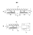
- FIG. 6 shows a capacitor provided with a trapezoidal electrolyte absorber.
- the electrolytic solution absorber 8-1 is disposed between the element end surface 52 and the sealing plate 14, avoiding the arrangement positions of the current collector plates 18-1 and 18-2.
- the electrolyte absorbent 8-1 is applied to the current collecting plate 18-1, the edges 34 and 36 of the current collecting plate 18-2, the second blocking walls 6-21 and 6-22, and the third blocking wall 6-30. It is sandwiched and fixed.
- the electrolytic solution absorbent 8-1 may be formed of a flexible sponge body or porous body. The excess electrolyte solution 4 staying in the outer case 12 is absorbed and held in the electrolyte solution absorbent 8-1.
- the shape of the electrolytic solution absorber 8-1 is a trapezoidal shape.
- the shape is not limited to this, and the amount of absorption of the desired electrolytic solution 4 and the current collecting plate 18-1 and the current collecting plate are not limited thereto.
- the size and shape may be appropriately changed depending on the size of the space between 18-2.
- the current collectors 18-1, 18-2 and the third blocking wall 6-30 are used as means for fixing the electrolyte absorbing material 8-1, but the present invention is not limited to this.
- it may be fixed by being sandwiched between the space portion 54 between the sealing plate 14 and the current collecting plates 18-1 and 18-2, or may be fixed using an adhesive.
- FIG. 7 shows a modification of the other electrolyte absorbent material 8-1.
- the electrolytic solution absorber 8-2 is arranged around the periphery of the sealing plate 14.
- the surplus electrolyte solution 4 staying in the outer case 12 is absorbed and held in the circulating electrolyte solution absorbent 8-2 regardless of the arrangement direction of the capacitor 2, so that the safety valve 16 It is possible to prevent the electrolytic solution 4 from adhering to.
- the electrolyte solution absorber 8-2 is arranged on the periphery, so that the degree of jumping up can be reduced.
- the electrolytic solution absorbent 8-2 is disposed around the inner wall of the outer case 12, the electrolytic solution 4 can be absorbed and held in the electrolytic solution absorbent 8-2. For this reason, the electrolytic solution 4 can be shut off from the safety valve 16 even when the capacitor 2 is horizontally arranged, inclined, or arranged such that the safety valve 16 is positioned downward.
- FIG. 8 shows the capacitor 2 provided with the electrolyte absorbent 8-1.
- the electrolytic solution absorber 8-1 is disposed in an insulating interval 56 between the current collector plates 18-1 and 18-2, and is sandwiched and fixed between at least the facing portion between the element end face 52 and the sealing plate 14. Yes. That is, one surface of the electrolytic solution absorber 8-1 is in contact with a part of the sealing plate 14 facing the inner side of the outer case 12, and the other surface is in contact with the element end surface 52 of the capacitor element 10.
- the capacitor 2 has first blocking walls 6-12 and 6-13 formed on the sealing plate 14 on one side facing the current collector plates 18-1 and 18-2.
- the second blocking walls 6-21 and 6-22 of the current collector plates 18-1 and 18-2 are disposed inside thereof.
- an electrolytic solution absorber 8-1 is inserted into the insulation interval 56 between the anode-side current collector 18-1 and the cathode-side current collector 18-2.
- the length L 1 of the electrolytic solution absorber 8-1 is formed to be longer than the facing distance L 2 between the element end face 52 and the sealing plate 14 within the insulating distance 56.
- the length L1 of the electrolytic solution absorber 8-1 before installation on the capacitor 2 is, for example, twice as long as the facing distance L2.
- the electrolytic solution absorbent 8-1 is compressed, for example, by pressing with a predetermined compressive force F from above and below and inserted into the insulating interval 56.
- a predetermined compressive force F from above and below and inserted into the insulating interval 56.
- the electrolytic solution absorber 8-1 When the electrolytic solution absorber 8-1 is inserted into the insulating interval 56, it is placed in a compressed state by a restoring force with respect to the compressive force F, and is pressed against the element end face 52 and the sealing plate 14 so that the electrolytic solution Demonstrate blocking function for 4
- the electrolyte absorbent 8-1 partially enters the gap 58 between the sealing plate 14 and the second blocking walls 6-21 and 6-22 as the compression is restored.
- a protruding portion 59 may be formed.
- the electrolyte absorbent 8-1 is disposed between the element end face 52 and the second blocking walls 6-21 and 6-22, which are the end faces of the current collecting plates 18-1 and 18-2, and the sealing plate 14. It is pinched and fixed.
- the protruding portion 59 has a gap 58 according to, for example, the lateral formation length of the electrolytic solution absorber 8-1 with respect to the lateral width of the insulating interval 56 and the ratio between the volume of the insulating interval 56 and the capacity of the electrolytic solution absorber 8-1. There may be a case where a part of the electrolyte absorbent 8-1 enters and is formed therein.
- the protruding portion 59 has a different length of entering the gap 58 depending on the hardness (viscosity) and restoring characteristics of the electrolyte absorbent material 8-1.
- the electrolytic solution absorbent 8-1 has, for example, a side portion on the edge 34 (36) of the current collectors 18-1 and 18-2 and the second blocking walls 6-21 and 6-6.
- the protrusion 59 is engaged with the gap 58 while being supported along ⁇ 22.
- the electrolyte absorbing material 8-1 is firmly fixed in the insulating interval 56.
- the capacitor 2 can block the inflow of the electrolyte 4 to the safety valve 16 by installing the electrolyte absorbent 8-1 in the insulation interval 56 and the gap 58.
- the electrolyte absorbing material 8-1 is compressed only in the gap 58 between the sealing plate 14 and the blocking wall 6-21 of the current collecting plate 18-1 and the blocking wall 6-22 of the current collecting plate 18-2. It may be inserted. That is, as shown in FIG. 11, for example, the capacitor 2 is electrolyzed inserted between the blocking wall 6-21 of the current collecting plate 18-1 and the blocking wall 6-22 of the current collecting plate 18-2 and the sealing plate 14.
- a liquid absorbent material 8-1 may be provided.
- the electrolytic solution absorber 8-1 is installed along the end surfaces of the blocking walls 6-21 and 6-22. Further, the electrolyte absorbent 8-1 is formed longer than the height of the gap 58, and may be compressed and inserted into the gap 58.
- the electrolyte absorbing material 8-1 is sandwiched and fixed between the blocking walls 6-21 and 6-22, which are the end surfaces of the current collecting plates 18-1 and 18-2, and the sealing plate.
- the electrolyte absorbing material 8-1 blocks the gap 58 between the blocking walls 6-21 and 6-22 and the sealing plate 14, so that the excess electrolyte 4 in the outer case 12 passes through the gap 58. The flow into the safety valve 16 side is blocked.
- the electrolyte absorbing material 8-1 is firmly fixed by compression between the blocking walls 6-21 and 6-22 and the sealing plate 14, it is fixed against an impact on the capacitor element 2 and continuous vibration. The state is maintained, and the blocking function of the electrolytic solution 4 can be maintained.
- the inserted electrolyte absorbing material 8-1 includes at least the sealing plate 14, the blocking wall 6-21 of the current collecting plate 18-1, and the blocking wall 6-22 of the current collecting plate 18-2. What is necessary is just to fix so that it may become a compression state in the clearance gap 58 of this.
- the electrolytic solution absorbent 8-1 is not limited to a quadrangular cross-sectional shape, and a part of the electrolytic solution absorbent 8-1 disposed between the blocking walls 6-21 and 6-22 and the sealing plate 14 is formed.
- the thickness of the portion may be longer than the height of the gap 58.
- the electrolytic solution absorber 8-1 may be formed, for example, so that the thickness of the portion disposed in the insulating interval 56 is equal to or smaller than the interval between the element end face 52 and the sealing plate 14.
- electrolyte absorbing material 8-1 in addition to blocking the gap 58 between the blocking walls 6-21, 6-22 and the sealing plate 14, the electrolyte solution 4 at the insulating interval 56 is absorbed to the safety valve 16 side. Can be prevented.
- the electrolytic solution absorbent 8-2 shown in FIG. 7 is similar to the electrolytic solution absorbent 8 having a large thickness with respect to the distance between the sealing plate 14 and the element end face 52 of the capacitor element 10. -2 may be inserted in a compressed state.
- electrolytic solution absorbers 8-1 and 8-2 are firmly bonded to the element end face 52 and the sealing plate 14 and firmly fixed, they are fixed against an impact on the capacitor element 2 and continuous vibration. Is maintained, and the blocking function by absorption of the electrolyte solution 4 can be maintained.
- the electrolyte absorbent 8-1 is compressed and inserted, and the gap 58 between the second blocking walls 6-21 and 6-22 and the sealing plate 14 is closed, so that the electrolyte absorbent 8-1 is electrolyzed.
- the liquid 4 can be retained, the electrolytic solution 4 can be prevented from jumping up, and the inflow of the electrolytic solution 4 to the safety valve 16 can be blocked.
- the current collecting plate 18- An interval may be provided between the second blocking walls 6-21 and 6-22 of the first and second 18-2 and the sealing plate 14, or these may be arranged in close contact with each other.
- the height of the third blocking wall 6-30 of the sealing plate 14 is set to the same height as the other first blocking walls 6-11, 6-12, 6-13, 6-14. However, it is not limited to this.
- the third blocking wall 6-30 is not positioned to face the current collecting plates 18-1 and 18-2. When arranged, it may extend to the element end face 52 of the capacitor element 10. By doing so, the path of the electrolytic solution 4 passing through the center of the capacitor element 10 can be further blocked.
- the current collecting plates 18-1 and 18-2 are fan-shaped, but the present invention is not limited to this.
- a semicircular shape may be used, and the shapes of the current collecting plate 18-1 and the current collecting plate 18-2 may be different.
- the surface of the convex portion 70 formed on the current collector plates 18-1 and 18-2 was used to connect the current collector plates 18-1 and 18-2 and the external terminals 24-1 and 24-2. Not limited to this.
- a part of the main body part 32 on the side of the arc part 38 may be cut out to form a current collector plate connection surface part, or the main body part 32 may be bent so that the center part becomes higher.
- the first blocking walls 6-11, 6-12, 6-13, and 6-14 are arranged inside the second blocking walls 6-21 and 6-22. Not exclusively.
- the first blocking walls 6-11, 6-12, 6-13, 6-14 and the second blocking walls 6-21, 6-22 are arranged at different positions. That is, the first blocking walls 6-11, 6-12, 6-13, 6-14 and the second blocking walls 6-21, 6-22 need not overlap, and the first blocking wall 6-
- the second blocking walls 6-21 and 6-22 may be disposed inside 11, 6-12, 6-13, and 6-14.
- the anode-side electrode overhanging portion 46-1 and the cathode-side electrode overhanging portion 46-2 are formed on one element end face 52 of the capacitor element 10, but the present invention is not limited thereto.
- the anode-side electrode protruding portion and the cathode-side electrode protruding portion may be formed on different element end faces.
- the safety valve 16 is used as the gas release mechanism, but the present invention is not limited to this.
- a through-hole may be formed in the sealing plate, a gas permeable membrane may be disposed so as to close the through-hole, or a valve structure in which a sealed state is opened when the internal pressure is increased may be used.
- the electrolyte solution 4 having fluidity is illustrated as an example of the electrolyte.
- the electrolyte includes an electrolyte solution whose fluidity is increased due to vibration when the capacitor 2 is driven. It is a waste.
- blocking wall is illustrated as an example of the interruption
- the present invention is not limited to this.
- the sealing plate 14 and the current collector plates 18-1 and 18-2 are connected while the electrolytic solution absorber 8-1 is compressed. You may let them.
- the invention of the present disclosure is provided with a gas release mechanism such as a safety valve in a sealing plate that seals an outer case enclosing a capacitor element, and the electrolyte staying in the outer case can be shut off from the gas release mechanism, and the valve function of the gas release mechanism by the electrolyte Can be widely used for capacitors such as electric double layer capacitors.
- a gas release mechanism such as a safety valve in a sealing plate that seals an outer case enclosing a capacitor element, and the electrolyte staying in the outer case can be shut off from the gas release mechanism, and the valve function of the gas release mechanism by the electrolyte Can be widely used for capacitors such as electric double layer capacitors.
Abstract
Description
4 電解液
6 遮断機構
6-11、6-12、6-13、6-14 第1の遮断壁
6-21、6-22 第2の遮断壁
6-30 第3の遮断壁
8-1 電解液吸収材
8-2 電解液吸収材
10 コンデンサ素子
12 外装ケース
14 封口板
16 安全弁
18-1、18-2 集電板
22 端子接続面部
24-1、24-2 外部端子
26 弁孔部
28 面部
30 面部
32 本体部
34 縁部
36 縁部
38 円弧部
40 円弧部
46-1、46-2 電極張出部
48 セパレータ
50 固定テープ
52 素子端面
54 空間部
56 絶縁間隔
58 隙間
59 突起部分
60 段部
62 弾性部
64 開口縁部
70 凸部
71 集電板接続面部
Claims (9)
- コンデンサ素子とともに電解質が収納された外装ケースと、該外装ケースを封口し外部端子が設置された封口板と、前記コンデンサ素子の素子端面に形成された電極張出部と前記外部端子との間に設置された集電板とを備えるコンデンサであって、
前記封口板に設置され前記外装ケース内のガスを放出するガス放出機構と、
少なくとも前記封口板または前記集電板のいずれか一方に設置され、前記ガス放出機構に対して前記電解質を遮断する遮断機構と
を備えることを特徴とするコンデンサ。 - 前記遮断機構は、
前記封口板に立設されて前記電解質を遮断する第1の遮断壁と、
前記集電板に立設されて前記電解質を遮断する第2の遮断壁とを含み、
前記第1の遮断壁に対して前記第2の遮断壁を異なる位置に備えることを特徴とする請求項1に記載のコンデンサ。 - 前記電極張出部は、前記素子端面の一方面部の異なる位置に陽極側の電極体と、陰極側の電極体とを張出させて形成され、
前記陽極側の前記電極張出部に陽極側の前記集電板、前記陰極側の電極張出部に陰極側の前記集電板を備えることを特徴とする請求項1または請求項2に記載のコンデンサ。 - 前記陽極側の前記集電板と前記陰極側の前記集電板との間に絶縁間隔を備え、該絶縁間隔内に前記電解質を遮断する第3の遮断壁を備えることを特徴とする請求項3に記載のコンデンサ。
- 前記ガス放出機構の対向位置に絶縁間隔を備えることを特徴とする請求項1ないし請求項4のいずれか1項に記載のコンデンサ。
- 前記電解質を吸収し、前記ガス放出機構に対する前記電解質を遮断する電解質吸収材を備えることを特徴とする請求項1ないし請求項5のいずれか1項に記載のコンデンサ。
- 前記電解質吸収材は、陽極側の前記集電板と陰極側の前記集電板の間に形成された絶縁間隔内に配置されていることを特徴とする請求項6に記載のコンデンサ。
- 前記電解質吸収材は、陽極側の前記集電板の縁部および前記第2の遮断壁と、陰極側の前記集電板の縁部および前記第2の遮断壁との間に挟み込まれて固定されることを特徴とする請求項7に記載のコンデンサ。
- 前記電解質吸収材は、前記素子端面および/または集電板の端面と、前記封口板との間に挟み込まれて固定されることを特徴とする請求項6ないし請求項8のいずれか1項に記載のコンデンサ。
Priority Applications (4)
| Application Number | Priority Date | Filing Date | Title |
|---|---|---|---|
| CN201480032071.8A CN105308699B (zh) | 2013-06-14 | 2014-06-12 | 电容器 |
| JP2015522549A JP6493205B2 (ja) | 2013-06-14 | 2014-06-12 | コンデンサ |
| EP14811742.7A EP3010029B1 (en) | 2013-06-14 | 2014-06-12 | Capacitor with gas release mechanism |
| US14/962,771 US9875856B2 (en) | 2013-06-14 | 2015-12-08 | Capacitor |
Applications Claiming Priority (2)
| Application Number | Priority Date | Filing Date | Title |
|---|---|---|---|
| JP2013-125626 | 2013-06-14 | ||
| JP2013125626 | 2013-06-14 |
Related Child Applications (1)
| Application Number | Title | Priority Date | Filing Date |
|---|---|---|---|
| US14/962,771 Continuation US9875856B2 (en) | 2013-06-14 | 2015-12-08 | Capacitor |
Publications (1)
| Publication Number | Publication Date |
|---|---|
| WO2014199639A1 true WO2014199639A1 (ja) | 2014-12-18 |
Family
ID=52021951
Family Applications (1)
| Application Number | Title | Priority Date | Filing Date |
|---|---|---|---|
| PCT/JP2014/003128 WO2014199639A1 (ja) | 2013-06-14 | 2014-06-12 | コンデンサ |
Country Status (5)
| Country | Link |
|---|---|
| US (1) | US9875856B2 (ja) |
| EP (1) | EP3010029B1 (ja) |
| JP (1) | JP6493205B2 (ja) |
| CN (1) | CN105308699B (ja) |
| WO (1) | WO2014199639A1 (ja) |
Cited By (6)
| Publication number | Priority date | Publication date | Assignee | Title |
|---|---|---|---|---|
| US20160118196A1 (en) * | 2014-10-28 | 2016-04-28 | Apaq Technology Co., Ltd. | Sealing element and wound-type solid state electrolytic capacitor thereof |
| EP3246928A4 (en) * | 2015-01-15 | 2018-08-22 | Ls Mtron Ltd. | External terminal, having structure for preventing leakage of electrolyte, for electric energy storage device |
| JP2021100756A (ja) * | 2015-03-06 | 2021-07-08 | 日東電工株式会社 | 水素排出膜 |
| JP2022509421A (ja) * | 2018-10-31 | 2022-01-20 | ティーディーケイ・エレクトロニクス・アクチェンゲゼルシャフト | キャパシタ |
| WO2023080144A1 (ja) * | 2021-11-02 | 2023-05-11 | 日本ケミコン株式会社 | 蓄電デバイスおよびその製造方法 |
| CN117174491A (zh) * | 2023-10-16 | 2023-12-05 | 东莞市爱伦电子科技有限公司 | 一种电解电容器 |
Families Citing this family (2)
| Publication number | Priority date | Publication date | Assignee | Title |
|---|---|---|---|---|
| JP6915485B2 (ja) * | 2016-09-28 | 2021-08-04 | 日本ケミコン株式会社 | コンデンサおよびその製造方法 |
| DE102019133565A1 (de) * | 2019-12-09 | 2021-06-10 | Tdk Electronics Ag | Elektrolytkondensator mit Kontrollelement zur Gasdiffusion |
Citations (5)
| Publication number | Priority date | Publication date | Assignee | Title |
|---|---|---|---|---|
| JPS55129447U (ja) | 1979-03-08 | 1980-09-12 | ||
| JP2004022233A (ja) * | 2002-06-13 | 2004-01-22 | Tookan:Kk | 危険防止機構付電池 |
| JP2011100998A (ja) | 2009-11-05 | 2011-05-19 | Samsung Electro-Mechanics Co Ltd | チップ型電気二重層キャパシタ及びその製造方法 |
| JP2012069644A (ja) * | 2010-09-22 | 2012-04-05 | Nippon Chemicon Corp | 電解コンデンサ |
| JP2013026462A (ja) * | 2011-07-21 | 2013-02-04 | Nippon Chemicon Corp | コンデンサ及びその製造方法 |
Family Cites Families (5)
| Publication number | Priority date | Publication date | Assignee | Title |
|---|---|---|---|---|
| JP2004071266A (ja) * | 2002-08-05 | 2004-03-04 | Sanyo Electric Co Ltd | 非水電解液二次電池及びその製造方法 |
| KR100599803B1 (ko) * | 2004-09-24 | 2006-07-12 | 삼성에스디아이 주식회사 | 이차 전지와 이에 사용되는 전극 조립체 및 집전판 |
| US7916454B2 (en) * | 2006-10-16 | 2011-03-29 | Panasonic Corporation | Capacitor |
| WO2012063486A1 (ja) | 2010-11-09 | 2012-05-18 | 日本ケミコン株式会社 | コンデンサ及びその製造方法 |
| JP5961940B2 (ja) * | 2011-07-21 | 2016-08-03 | 日本ケミコン株式会社 | コンデンサの製造方法 |
-
2014
- 2014-06-12 CN CN201480032071.8A patent/CN105308699B/zh active Active
- 2014-06-12 WO PCT/JP2014/003128 patent/WO2014199639A1/ja active Application Filing
- 2014-06-12 JP JP2015522549A patent/JP6493205B2/ja active Active
- 2014-06-12 EP EP14811742.7A patent/EP3010029B1/en active Active
-
2015
- 2015-12-08 US US14/962,771 patent/US9875856B2/en active Active
Patent Citations (5)
| Publication number | Priority date | Publication date | Assignee | Title |
|---|---|---|---|---|
| JPS55129447U (ja) | 1979-03-08 | 1980-09-12 | ||
| JP2004022233A (ja) * | 2002-06-13 | 2004-01-22 | Tookan:Kk | 危険防止機構付電池 |
| JP2011100998A (ja) | 2009-11-05 | 2011-05-19 | Samsung Electro-Mechanics Co Ltd | チップ型電気二重層キャパシタ及びその製造方法 |
| JP2012069644A (ja) * | 2010-09-22 | 2012-04-05 | Nippon Chemicon Corp | 電解コンデンサ |
| JP2013026462A (ja) * | 2011-07-21 | 2013-02-04 | Nippon Chemicon Corp | コンデンサ及びその製造方法 |
Cited By (11)
| Publication number | Priority date | Publication date | Assignee | Title |
|---|---|---|---|---|
| US20160118196A1 (en) * | 2014-10-28 | 2016-04-28 | Apaq Technology Co., Ltd. | Sealing element and wound-type solid state electrolytic capacitor thereof |
| EP3246928A4 (en) * | 2015-01-15 | 2018-08-22 | Ls Mtron Ltd. | External terminal, having structure for preventing leakage of electrolyte, for electric energy storage device |
| US10074488B2 (en) | 2015-01-15 | 2018-09-11 | Ls Mtron Ltd. | External terminal, having structure for preventing leakage of electrolyte, for electric energy storage device |
| JP2021100756A (ja) * | 2015-03-06 | 2021-07-08 | 日東電工株式会社 | 水素排出膜 |
| JP7034577B2 (ja) | 2015-03-06 | 2022-03-14 | 日東電工株式会社 | 水素排出膜 |
| JP7181324B2 (ja) | 2015-03-06 | 2022-11-30 | 日東電工株式会社 | 水素排出膜 |
| JP2022509421A (ja) * | 2018-10-31 | 2022-01-20 | ティーディーケイ・エレクトロニクス・アクチェンゲゼルシャフト | キャパシタ |
| US11501925B2 (en) | 2018-10-31 | 2022-11-15 | Tdk Electronics Ag | Capacitor |
| WO2023080144A1 (ja) * | 2021-11-02 | 2023-05-11 | 日本ケミコン株式会社 | 蓄電デバイスおよびその製造方法 |
| CN117174491A (zh) * | 2023-10-16 | 2023-12-05 | 东莞市爱伦电子科技有限公司 | 一种电解电容器 |
| CN117174491B (zh) * | 2023-10-16 | 2024-01-26 | 东莞市爱伦电子科技有限公司 | 一种电解电容器 |
Also Published As
| Publication number | Publication date |
|---|---|
| EP3010029A1 (en) | 2016-04-20 |
| CN105308699B (zh) | 2018-04-06 |
| JPWO2014199639A1 (ja) | 2017-02-23 |
| US9875856B2 (en) | 2018-01-23 |
| EP3010029A4 (en) | 2017-04-26 |
| JP6493205B2 (ja) | 2019-04-03 |
| CN105308699A (zh) | 2016-02-03 |
| EP3010029B1 (en) | 2021-01-06 |
| US20160093450A1 (en) | 2016-03-31 |
Similar Documents
| Publication | Publication Date | Title |
|---|---|---|
| JP6493205B2 (ja) | コンデンサ | |
| JP5317129B2 (ja) | 2次電池 | |
| US7031140B2 (en) | Electric double layer capacitor, electrolytic cell and process for fabricating same | |
| JP2019186187A (ja) | 蓄電モジュール | |
| WO2019151359A1 (ja) | 蓄電素子 | |
| KR102555959B1 (ko) | 외부접속단자를 갖는 전기화학 에너지 저장장치 | |
| JP4451654B2 (ja) | リチウム二次電池 | |
| JP6269198B2 (ja) | 蓄電素子及び蓄電素子の製造方法 | |
| JP7079693B2 (ja) | 蓄電モジュール、蓄電装置、及び蓄電モジュールの製造方法 | |
| KR20230136546A (ko) | 전지 케이스 및 해당 전지 케이스를 구비하는 이차 전지 | |
| JP2005166974A (ja) | 電気二重層コンデンサ、電解質電池及びこれらの製造方法 | |
| JP6785728B2 (ja) | 蓄電装置 | |
| JP2021015771A (ja) | 蓄電装置 | |
| JP2020136244A (ja) | 蓄電素子 | |
| JP2020030985A (ja) | 蓄電モジュール | |
| WO2007123033A1 (ja) | 電気二重層キャパシタ | |
| JP2004022339A (ja) | 電池 | |
| JP6926509B2 (ja) | 蓄電装置 | |
| JP2017084540A (ja) | 蓄電素子 | |
| JP2020030984A (ja) | 蓄電モジュール | |
| JP2020030951A (ja) | 蓄電モジュール | |
| JP2020030982A (ja) | 蓄電モジュール | |
| JP2020030983A (ja) | 蓄電モジュール | |
| JP6502609B2 (ja) | 蓄電素子 | |
| JP6942079B2 (ja) | 蓄電モジュール |
Legal Events
| Date | Code | Title | Description |
|---|---|---|---|
| WWE | Wipo information: entry into national phase |
Ref document number: 201480032071.8 Country of ref document: CN |
|
| 121 | Ep: the epo has been informed by wipo that ep was designated in this application |
Ref document number: 14811742 Country of ref document: EP Kind code of ref document: A1 |
|
| ENP | Entry into the national phase |
Ref document number: 2015522549 Country of ref document: JP Kind code of ref document: A |
|
| NENP | Non-entry into the national phase |
Ref country code: DE |
|
| REEP | Request for entry into the european phase |
Ref document number: 2014811742 Country of ref document: EP |
|
| WWE | Wipo information: entry into national phase |
Ref document number: 2014811742 Country of ref document: EP |