WO2014184877A1 - スクリーン印刷機 - Google Patents
スクリーン印刷機 Download PDFInfo
- Publication number
- WO2014184877A1 WO2014184877A1 PCT/JP2013/063440 JP2013063440W WO2014184877A1 WO 2014184877 A1 WO2014184877 A1 WO 2014184877A1 JP 2013063440 W JP2013063440 W JP 2013063440W WO 2014184877 A1 WO2014184877 A1 WO 2014184877A1
- Authority
- WO
- WIPO (PCT)
- Prior art keywords
- screen
- squeegee
- solder
- printing
- head
- Prior art date
Links
Images


Classifications
-
- B—PERFORMING OPERATIONS; TRANSPORTING
- B41—PRINTING; LINING MACHINES; TYPEWRITERS; STAMPS
- B41F—PRINTING MACHINES OR PRESSES
- B41F15/00—Screen printers
- B41F15/08—Machines
- B41F15/0881—Machines for printing on polyhedral articles
-
- B—PERFORMING OPERATIONS; TRANSPORTING
- B41—PRINTING; LINING MACHINES; TYPEWRITERS; STAMPS
- B41F—PRINTING MACHINES OR PRESSES
- B41F15/00—Screen printers
- B41F15/08—Machines
- B41F15/12—Machines with auxiliary equipment, e.g. for drying printed articles
-
- B—PERFORMING OPERATIONS; TRANSPORTING
- B41—PRINTING; LINING MACHINES; TYPEWRITERS; STAMPS
- B41F—PRINTING MACHINES OR PRESSES
- B41F15/00—Screen printers
- B41F15/14—Details
- B41F15/40—Inking units
- B41F15/42—Inking units comprising squeegees or doctors
-
- B—PERFORMING OPERATIONS; TRANSPORTING
- B41—PRINTING; LINING MACHINES; TYPEWRITERS; STAMPS
- B41F—PRINTING MACHINES OR PRESSES
- B41F15/00—Screen printers
- B41F15/14—Details
- B41F15/40—Inking units
- B41F15/42—Inking units comprising squeegees or doctors
- B41F15/423—Driving means for reciprocating squeegees
-
- B—PERFORMING OPERATIONS; TRANSPORTING
- B41—PRINTING; LINING MACHINES; TYPEWRITERS; STAMPS
- B41F—PRINTING MACHINES OR PRESSES
- B41F15/00—Screen printers
- B41F15/14—Details
- B41F15/44—Squeegees or doctors
-
- B—PERFORMING OPERATIONS; TRANSPORTING
- B41—PRINTING; LINING MACHINES; TYPEWRITERS; STAMPS
- B41F—PRINTING MACHINES OR PRESSES
- B41F15/00—Screen printers
- B41F15/14—Details
- B41F15/44—Squeegees or doctors
- B41F15/46—Squeegees or doctors with two or more operative parts
-
- B—PERFORMING OPERATIONS; TRANSPORTING
- B41—PRINTING; LINING MACHINES; TYPEWRITERS; STAMPS
- B41F—PRINTING MACHINES OR PRESSES
- B41F33/00—Indicating, counting, warning, control or safety devices
- B41F33/02—Arrangements of indicating devices, e.g. counters
-
- H—ELECTRICITY
- H05—ELECTRIC TECHNIQUES NOT OTHERWISE PROVIDED FOR
- H05K—PRINTED CIRCUITS; CASINGS OR CONSTRUCTIONAL DETAILS OF ELECTRIC APPARATUS; MANUFACTURE OF ASSEMBLAGES OF ELECTRICAL COMPONENTS
- H05K3/00—Apparatus or processes for manufacturing printed circuits
- H05K3/10—Apparatus or processes for manufacturing printed circuits in which conductive material is applied to the insulating support in such a manner as to form the desired conductive pattern
- H05K3/12—Apparatus or processes for manufacturing printed circuits in which conductive material is applied to the insulating support in such a manner as to form the desired conductive pattern using thick film techniques, e.g. printing techniques to apply the conductive material or similar techniques for applying conductive paste or ink patterns
- H05K3/1216—Apparatus or processes for manufacturing printed circuits in which conductive material is applied to the insulating support in such a manner as to form the desired conductive pattern using thick film techniques, e.g. printing techniques to apply the conductive material or similar techniques for applying conductive paste or ink patterns by screen printing or stencil printing
- H05K3/1233—Methods or means for supplying the conductive material and for forcing it through the screen or stencil
-
- H—ELECTRICITY
- H05—ELECTRIC TECHNIQUES NOT OTHERWISE PROVIDED FOR
- H05K—PRINTED CIRCUITS; CASINGS OR CONSTRUCTIONAL DETAILS OF ELECTRIC APPARATUS; MANUFACTURE OF ASSEMBLAGES OF ELECTRICAL COMPONENTS
- H05K3/00—Apparatus or processes for manufacturing printed circuits
- H05K3/30—Assembling printed circuits with electric components, e.g. with resistor
- H05K3/32—Assembling printed circuits with electric components, e.g. with resistor electrically connecting electric components or wires to printed circuits
- H05K3/34—Assembling printed circuits with electric components, e.g. with resistor electrically connecting electric components or wires to printed circuits by soldering
-
- H—ELECTRICITY
- H05—ELECTRIC TECHNIQUES NOT OTHERWISE PROVIDED FOR
- H05K—PRINTED CIRCUITS; CASINGS OR CONSTRUCTIONAL DETAILS OF ELECTRIC APPARATUS; MANUFACTURE OF ASSEMBLAGES OF ELECTRICAL COMPONENTS
- H05K2203/00—Indexing scheme relating to apparatus or processes for manufacturing printed circuits covered by H05K3/00
- H05K2203/16—Inspection; Monitoring; Aligning
- H05K2203/163—Monitoring a manufacturing process
-
- H—ELECTRICITY
- H05—ELECTRIC TECHNIQUES NOT OTHERWISE PROVIDED FOR
- H05K—PRINTED CIRCUITS; CASINGS OR CONSTRUCTIONAL DETAILS OF ELECTRIC APPARATUS; MANUFACTURE OF ASSEMBLAGES OF ELECTRICAL COMPONENTS
- H05K3/00—Apparatus or processes for manufacturing printed circuits
- H05K3/30—Assembling printed circuits with electric components, e.g. with resistor
- H05K3/32—Assembling printed circuits with electric components, e.g. with resistor electrically connecting electric components or wires to printed circuits
- H05K3/34—Assembling printed circuits with electric components, e.g. with resistor electrically connecting electric components or wires to printed circuits by soldering
- H05K3/3457—Solder materials or compositions; Methods of application thereof
- H05K3/3485—Applying solder paste, slurry or powder
Definitions
- the present invention relates to a screen printer that performs printing by moving a solder placed on a screen with a squeegee.
- a reflective photoelectric switch is attached to a squeegee holding device that can hold a squeegee and move parallel to the screen, and solder on the screen based on a detection signal from the photoelectric switch.
- a squeegee holding device that can hold a squeegee and move parallel to the screen, and solder on the screen based on a detection signal from the photoelectric switch.
- the squeegee holding device is moved along the screen so that the optical axis of the photoelectric switch passes through the solder, and the interval between the two positions when the detection signal of the photoelectric switch changes ( (Movement distance) is calculated as the roll width of the solder, that is, the amount of solder.
- the time for measuring the amount of solder becomes longer by the moving time. Since the amount of solder on the screen has a large effect on the print quality, it is desirable to measure the amount of solder as frequently as possible (for example, every time printing is performed). Therefore, it is difficult to frequently measure the amount of solder.
- the main purpose of the screen printing machine of the present invention is to shorten the time for measuring the amount of solder.
- the screen printing machine of the present invention employs the following means in order to achieve the main object described above.
- the screen printing machine of the present invention is A screen printing machine that performs printing by moving solder placed on a screen with a squeegee, A head on which the squeegee is mounted; Translation means for relatively moving the head and the screen in a direction parallel to the screen; Vertical moving means for relatively moving the head and the screen in a direction perpendicular to the screen; Position detecting means for detecting a relative position between the squeegee and the screen; An optical detection means provided so that the optical axis position can be moved relative to the screen by the parallel movement means, and the screen and the solder at the optical axis position are detected in an identifiable manner; When printing is completed, the vertical movement means is controlled so that the squeegee and the screen move relative to each other in a direction perpendicular to the screen from a state where the squeegee is at least separated from a state in contact with one end of the solder in the printing direction.
- the parallel movement means is controlled so that the head and the screen relatively move in a direction parallel to the screen until at least the other end of the solder in the printing direction is detected by the optical detection means.
- Printing end control means The relative position between the squeegee and the screen detected by the position detection unit when printing is completed and the other end in the printing direction of the solder are detected by the position detection unit when detected by the optical detection unit.
- Solder amount estimating means for estimating the amount of solder on the screen based on the relative position between the squeegee and the screen; It is a summary to provide.
- the optical axis position is movable relative to the screen, and the optical detection means for detecting the screen and the solder at the optical axis position so as to be identifiable is provided.
- the head and the screen are relatively moved in a direction perpendicular to the screen from the state in contact with one end of the solder printing direction to a position separated from the position, and then at least the other end of the solder printing direction is detected by the optical detection means.
- the head and the screen are moved relative to each other in a direction parallel to the screen.
- the amount of solder on the screen based on the relative position between the squeegee and the screen when printing is completed and the relative position between the squeegee and the screen when the other end of the solder printing direction is detected by the optical detection means. Is estimated.
- the movement distance of the optical detection means can be shortened as compared with the case where the optical detection means is moved so that the optical axis completely passes through the solder, so that the movement time can be shortened.
- the time for measuring the amount of solder can be further shortened.
- the squeegee includes a first squeegee and a second squeegee arranged so that contact surfaces with the solder face each other, and the first squeegee is brought into contact with the solder to connect the head and the screen to the first squeegee.
- the second squeegee is brought into contact with the solder, and the head and the screen are moved relative to each other in a second direction opposite to the first direction.
- the optical detection means finishes printing by the first squeegee, and the optical detection means moves the other end of the solder in the printing direction.
- the other end side of the solder in the printing direction is the second squeegee. It may be composed provided so as to be positioned below and in the vicinity. By doing this, it is possible to shorten the time from the completion of the estimation of the solder amount to the start of the next printing, and it is possible to increase the printing amount per unit time.
- FIG. 1 is an external perspective view showing an external appearance of a component assembly system 10.
- FIG. 1 is a configuration diagram showing an outline of a configuration of a screen printing machine 20 of a present embodiment incorporated in a component assembly system 10.
- FIG. 2 is a configuration diagram showing an outline of the configuration of squeegee units 30 and 40.
- 3 is a block diagram showing an electrical connection relationship between a management computer 90 and the screen printer 20.
- FIG. 6 is a flowchart illustrating an example of a print processing routine. It is a flowchart which shows an example of a solder amount estimation process routine. It is explanatory drawing explaining the mode of operation
- FIG. 1 is an external perspective view showing an external appearance of a component assembly system 10
- FIG. 2 is a configuration diagram showing an outline of the configuration of a screen printer 20 as an embodiment of the present invention incorporated in the component assembly system 10.
- FIG. 3 is a block diagram showing an outline of the configuration of the squeegee units 30 and 40
- FIG. 4 is a block diagram showing an electrical connection relationship between the management computer 90 and the screen printer 20.
- the component assembly system 10 includes a plurality of (two in this embodiment) screen printers 20 that form a wiring pattern on a circuit board P (see FIG. 2) by screen printing, and screen printing.
- a control device 70 for controlling the machine 20 a plurality of (7 in this embodiment) electronic component mounting machines 80 for mounting electronic components on the circuit board P on which the wiring pattern is formed by the screen printing machine 20,
- a control device 82 that controls the electronic component mounting machine 80 and a management computer 90 that manages the control devices 70 and 82 are provided.
- the circuit board P is transported by the substrate transport device 12 (see FIG. 4), and the plurality of screen printing machines 20 and the plurality of electronic component mounting machines 80 are screened in the transport direction on the transport path.
- the printing machines 20 are arranged side by side so as to be upstream from the electronic component mounting machine 80.
- the plurality of screen printing machines 20 have the same configuration, the same reference numerals are given. Since a plurality of electronic component mounting machines and their control devices do not form the gist of the present invention, they are collectively denoted by reference numerals “80” and “82”, and detailed descriptions thereof are omitted.
- the screen printing machine 20 uses a screen S while rolling the solder on the screen S using the squeegees 32 and 42 (see FIG. 3) as a pre-process of mounting the electronic component by the electronic component mounting machine 80.
- the solder is applied (printed) to the lower circuit board P through the pattern hole by being pressed into the pattern hole formed in the housing.
- a printing machine main body 24 installed at 22.
- the left-right direction in FIG. 2 is the printing direction
- the front (front) and rear (back) directions indicate the conveyance direction of the circuit board P.
- the printing machine main body 24 is installed on a base portion 22 a that is a lower portion of the housing 22 and holds a circuit board P that is transported from the back to the front of FIG. 2,
- a screen support base 28 installed at the middle stage of the housing 22 and supporting the screen S in a horizontal posture
- a pair of left and right squeegee units 30 and 40 installed at the upper stage of the housing 22, and a pair of squeegee units 30,
- the horizontal movement apparatus 50 which moves 40 to a horizontal direction (FIG. 2 left-right direction) along the screen S, and the photoelectric sensor 60 for detecting the solder on the screen S are provided.
- the squeegee units 30 and 40 each have a squeegee 32 and 42 as rectangular plate-like members, and a squeegee holding unit that holds the squeegees 32 and 42 while being inclined at a predetermined angle with respect to the screen S.
- Squeegee heads 34 and 44 as members and elevating devices 36 and 46 for raising and lowering the squeegees 32 and 42 via the squeegee heads 34 and 44 are provided.
- the squeegees 32 and 42 are arranged so that the contact surfaces with the solder rolls face each other, and are configured as double squeegees capable of reciprocal printing by reciprocating in a direction perpendicular to the longitudinal direction.
- the squeegee 32 disposed on the right side of FIG. 3 is also referred to as a right squeegee
- the squeegee 42 disposed on the left side of FIG. 3 is also referred to as a left squeegee.
- the squeegee heads 34 and 44 are configured so that the squeegees 32 and 42 can be attached and detached.
- the inclination angle (squeegee angle) with respect to the screen S can be adjusted.
- the elevating devices 36 and 46 are configured as air cylinders that can push the piston rods 36a and 46a downward by air pressure. Has been.
- the horizontal movement device 50 includes a slider 52 to which the squeegee units 30 and 40 are fixed, a ball screw nut 54 attached to the slider 52, and a screw that passes through the ball screw nut 54 in the axial direction. It is configured as a linear feed mechanism including a shaft 56 and a horizontal movement drive motor 58 (see FIG. 4) whose rotation shaft is coupled to the screw shaft 56.
- the screw shaft 56 is arranged in a direction orthogonal to the conveyance direction of the circuit board P and in a direction parallel to the screen S.
- the screw shaft 56 guides the movement of the slider 52 in parallel with the screw shaft 56 (not shown). Guide rails are arranged.
- the squeegee units 30 and 40 are fixed to the slider 52 as described above, the squeegee units 30 and 40 are driven in the direction orthogonal to the conveying direction of the circuit board P by driving the horizontal movement drive motor 58. In addition, it can be moved in a direction parallel to the screen S.
- the horizontal movement drive motor 58 is configured as a servo motor that can be driven in both forward and reverse rotations. During forward rotation drive, the squeegee units 30 and 40 are moved in the forward movement direction (left direction in FIG. 2) to perform reverse rotation. During driving, the squeegee units 30 and 40 are moved in the backward movement direction (right direction in FIG. 2).
- the horizontal movement device 50 is also provided with an encoder 59 (see FIG. 4) for detecting the movement position of the slider 52 in the horizontal direction (printing direction), that is, the movement position of the squeegees 32 and 42.
- the photoelectric sensor 60 is configured as a reflective photoelectric sensor having a projector and a light receiver, and receives the reflected light of the light projected from the projector toward the screen S by the light receiver.
- the presence or absence of an object (solder roll) on the screen S is detected.
- the reflectance of the surface of the screen S is different from that of the solder roll.
- the photoelectric sensor 60 receives the reflected light of the light projected from the light projector, the presence or absence of the solder roll at the light projection position (optical axis position) on the screen S based on the amount of the received light. Can be detected.
- the photoelectric sensor 60 is fixed to the slider 52 via a fixture 62, and moves together with the squeegee units 30 and 40 as the slider 52 moves.
- the fixture 62 has a rectangular fixing member 64 fixed to the slider 52, a long portion 66a and a short portion 66b, and the photoelectric sensor 60 is fixed to the short portion 66b.
- An L-shaped fixing member 66 and an attachment main body 68 attached to the fixing member 64 at the upper part and attached to the fixing member 66 at the lower part are provided.
- the attachment main body 68 has two elongated holes 68a formed in the horizontal direction in the upper part, and the fixing member 64 is attached by bolts 65a through the elongated holes 68a.
- the fixture main body 68 is formed with an arc hole 68b and a round hole in the lower part, and the longitudinal portion 66a of the fixing member 66 is attached by bolts 65b and 65c through the arc hole 68b and the round hole, respectively. ing. Therefore, the installation position of the photoelectric sensor 60 in the horizontal direction (printing direction) can be adjusted depending on the position in the elongated hole 68a where the bolt 65a is fixed, and the position in the arc hole 68b where the bolt 65b is fixed. Thus, the optical axis angle of the photoelectric sensor 60 with respect to the screen S can be adjusted. In this embodiment, the photoelectric sensor 60 adjusts the horizontal position and the optical axis angle so that the optical axis position on the screen S is located below the left squeegee 42. The reason for this will be described later.
- the control device 70 is configured as a microprocessor centered on a CPU 71, and includes a ROM 72 that stores processing programs, an HDD 73 that stores various data, a RAM 74 that is used as a work area, an external device and an electrical device.
- An input / output interface 75 for exchanging signals is provided, and these are electrically connected via a bus 76.
- a detection signal from the photoelectric sensor 60 and a detection signal from the encoder 59 are input to the control device 70 via the input / output interface 75.
- control device 70 inputs / outputs a drive signal to the substrate transfer device 12, a drive signal to the substrate holding device 26, a drive signal to the horizontal movement drive motor 58, a drive signal to the lifting devices 36 and 46, and the like.
- the data is output via the interface 75.
- the control device 70 is connected to the management computer 90 so as to be capable of two-way communication, and exchanges control commands and data with each other.
- the management computer 90 is configured as a microprocessor centered on a CPU 91, and includes a ROM 92 that stores a processing program, an HDD 93 that stores a production plan for the circuit board P, and a RAM 94 that is used as a work area.
- An input / output interface 95 for exchanging electrical signals with an external device is provided, and these are connected via a bus 96.
- the management computer 90 inputs operation signals from an input device 97 typified by a mouse or a keyboard via an input / output interface 95, and outputs various images to the display 98 via the input / output interface 95. .
- the production plan of the circuit board P means what kind of wiring pattern is formed on which circuit board P in each screen printing machine 20 and what electronic components are mounted on the circuit board P in each electronic component mounting machine 80. Or a plan that defines how many circuit boards P (assemblies) on which electronic components are mounted are to be produced.
- the management computer 90 receives a production plan from the operator via the input device 97 and transmits various commands to the screen printing machine 20 and the electronic component mounting machine 80 so that an assembly is produced according to the received production plan.
- FIG. 5 is a flowchart illustrating an example of a print processing routine executed by the CPU 71 of the control device 70. This routine is executed when a screen printing command is received from the management computer 90.
- the CPU 71 of the control device 70 first drives and controls the horizontal movement drive motor 58 so that the right squeegee 32 moves to the print start position (step S100). Subsequently, the elevating device 36 is driven and controlled so as to descend until the right squeegee 32 comes in contact with the screen S (step S110), and the right squeegee 32 is moved forward by driving the horizontal movement drive motor 58 to rotate forward (FIG. 2). The forward printing is performed to print the solder on the circuit board P that has been moved to the left and conveyed by the board conveying device 12 (step S120).
- step S130 When the forward printing is completed (step S130), the elevating device 36 is driven and controlled so that the right squeegee 32 rises from the state in contact with one end (right end) R1 of the solder roll to the position separated (step S140). It is determined whether or not printing for the number of sheets designated by the computer 90 has been completed (step S150). If it is determined that printing for the designated number of sheets has been completed, the printing process is terminated. If it is determined that printing for the number of designated sheets has not been completed, a solder amount estimation process is executed (step S160).
- the solder amount estimation processing is processing for estimating the amount of solder remaining on the screen S (solder roll width R) using the photoelectric sensor 60, and is described later in FIG. This is done by executing
- the elevating device 46 is driven and controlled to descend until the left squeegee 42 contacts the other end (left end) R2 of the solder roll in the printing direction (step S170), and the horizontal movement drive motor 58 is reversed.
- the left squeegee 42 moves backward (moves in the right direction in FIG. 2), and backward printing is performed to print solder on the circuit board P that has been transported next (step S180).
- the elevating device 46 is driven and controlled so that the left squeegee 42 ascends from the state in contact with the left end R2 of the solder roll to the separated position (step S200).
- step S210 It is determined whether or not printing for the number of sheets has been completed (step S210). If it is determined that printing for the designated number of pages has not been completed, the process returns to step S110 to execute forward printing on the circuit board P transported next (steps S110 to S140). If it is determined that the printing for the minute is finished, the printing process is finished.
- the solder amount estimation process of FIG. 6 will be described.
- the squeegee position p1 which is the position of the squeegees 32 and 42 when the forward printing is finished, is input from the encoder 59 (step S300).
- the horizontal movement drive motor 58 is driven in the reverse rotation to start the backward movement of the slider 52 (step S310), and waits for the photoelectric sensor 60 to detect the left end R2 of the solder roll (step S320).
- the photoelectric sensor 60 is fixed to the slider 50 together with the squeegees 32 and 42, when the slider 50 moves, the photoelectric sensor 60 moves accordingly.
- the slider 52 stops moving backward (step S330), and the squeegees 32 and 34 are positioned when the photoelectric sensor 60 detects the left end R2 of the solder roll.
- the position p2 is input from the encoder 59 (step S340).
- the solder roll width R is calculated by the following equation (1) (step S360).
- “X” in the formula (1) indicates a horizontal distance from the right squeegee 32 to the optical axis position on the screen S of the photoelectric sensor 60. Since both the right squeegee 32 and the photoelectric sensor 60 are fixed to the slider 52, the distance X can be obtained in advance.
- the photoelectric sensor 60 is moved so that the optical axis passes through the right end R1 and the left end R2 of the solder roll, and the solder roll width R is not directly estimated from the movement amount, but the right end R1 of the solder roll.
- the photoelectric sensor 60 is arranged so that the optical axis on the screen S is positioned at a distance X away from the right squeegee 32 in contact with the sensor, and the photoelectric sensor 60 detects the left end R2 of the solder roll from the photoelectric sensor 60.
- the solder roll width R is estimated by subtracting the movement amount S of 60 from the distance X.
- the moving distance of the photoelectric sensor 60 (slider 52) until the photoelectric sensor 60 detects the left end R2 of the solder roll can be shortened.
- the execution time of the estimation process can be shortened.
- the solder roll width R is thus calculated, it is determined whether or not the calculated solder roll width R is less than the threshold value Rref (step S370).
- the threshold value Rref is determined in the vicinity of a lower limit value within an appropriate range of the amount of solder that can stably perform screen printing. If it is determined that the solder roll width R is greater than or equal to the threshold value Rref, the solder on the screen S is determined to be within the appropriate range, the solder amount estimation process is terminated, and if the solder roll width R is determined to be less than the threshold value Rref, It is determined that the solder is insufficient, a predetermined warning is output (step S380), and the solder amount estimation process is terminated.
- step S380 is performed by transmitting a warning signal to the management computer 90 by the control device 70, and the management computer 90 that has received the warning signal displays a warning screen requesting replenishment of solder on the display 98.
- the automatic supply device is controlled so that the solder is appropriately replenished based on the estimated solder roll width R. It may be a thing.
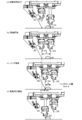
- FIG. 7 is an explanatory diagram for explaining the operation of the screen printer 20 when the solder roll width R is estimated.
- the right squeegee 32 is in contact with the right end R1 of the solder roll (see FIG. 7A).
- the right squeegee 32 is raised, and the squeegees 32 and 42 (photoelectric sensor 60) start moving backward (moving in the right direction in the figure) (see FIG. 7B).
- the optical axis position on the screen S of the photoelectric sensor 60 is below the right squeegee 32, that is, at a position separated from the right end R1 of the solder roll by the distance X.
- the photoelectric sensor 60 When the squeegees 32 and 42 (photoelectric sensor 60) are moved until the photoelectric sensor 60 detects the left end R2 of the solder roll (see FIG. 7C), the photoelectric sensor 60 is moved to the left end of the solder roll from the end of forward printing.
- the next backward printing is started by lowering the left squeegee 42 and moving it to the right (see FIG. 7D).
- the photoelectric sensor 60 adjusts the optical axis so that the optical axis position on the screen S is located below the left squeegee 42. Therefore, when the photoelectric sensor 60 detects the left end R2 of the solder roll, The squeegee 42 is positioned above the left end R2 of the solder roll. For this reason, the left squeegee 42 can be brought into contact with the left end R2 of the solder roll only by lowering the left squeegee 42, and the backward printing can be started quickly.
- forward printing is performed in which the photoelectric sensor 60 and the squeegees 32 and 42 are fixed to the slider 52, and the solder on the screen S is rolled by the forward movement of the right squeegee 32.
- the right squeegee 32 is moved away from the state in contact with the right end R1 of the solder roll and the squeegee position p1 at that time is input.
- the slider 52 photoelectric sensor
- the photoelectric sensor 60 detects the left end R2 of the solder roll. 60
- the squeegee position p2 at that time is input.
- the movement amount S from the squeegee position p1 to the squeegee position p2 is subtracted from the distance (horizontal distance) X from the right squeegee 32 to the optical axis position on the screen S of the photoelectric sensor 60, thereby remaining on the screen S.
- the amount of solder (solder roll width R) is calculated.
- the movement distance (movement amount S) of the photoelectric sensor 60 necessary for calculating the solder roll width R is made shorter than the movement distance necessary for the photoelectric sensor 60 to pass from the right end R1 to the left end R2 of the solder roll. Therefore, the time required for estimating the solder roll width can be further shortened.
- the execution frequency of the solder amount estimation process can be increased without significantly reducing the number of printed sheets per unit time, and the solder amount on the screen S can be managed more appropriately.
- the optical axis is adjusted so that the optical axis position on the screen S of the photoelectric sensor 60 is positioned below the left squeegee 42, when the photoelectric sensor 60 detects the left end R2 of the solder roll, the left squeegee 42 It can be located above the left end R2 of the solder roll. Therefore, after executing the solder amount estimation process, the left squeegee 42 can be brought into contact with the left end R2 of the solder roll simply by lowering the left squeegee 42, and the backward printing can be started quickly.
- the optical axis is adjusted so that the optical axis position on the screen S of the photoelectric sensor 60 is positioned below the left squeegee 42.
- the optical axis position on the screen S is not necessarily limited. It is not necessary to be located below the left squeegee 42. However, the closer the optical axis position on the screen S is to the lower side of the left squeegee 42, the shorter the moving distance of the left squeegee 42 to the reverse printing start position, so the time until the next reverse printing is started is shortened. Can be made.
- the solder amount estimation process is executed every time forward printing is finished.
- the present invention is not limited to this, and the solder amount is obtained every time a predetermined number of prints are finished. Execute the estimation process or change the timing to execute the next solder amount estimation process based on the solder amount estimated in the solder amount estimation process (for example, the smaller the estimated solder amount, the more the solder amount estimation process).
- the solder amount estimation processing may be executed at any frequency, for example, by shortening the execution interval.
- the solder amount is estimated after the forward printing is finished.
- the invention is not limited to this, and the solder amount is estimated after the backward printing is finished.
- the solder amount may be estimated both after the forward printing is finished and after the backward printing is finished.
- the photoelectric sensor is arranged so that the optical axis on the screen S is positioned at a distance (horizontal distance) X away from the left squeegee 42 in the backward movement direction (right direction). Should be installed.
- the two squeegees 32 and 42 are configured to be able to perform reciprocal printing.
- the present invention is not limited to this, and one squeegee can perform printing in only one direction. It may be configured.
- the screen S is executed by fixing the screen S to the housing 22 and moving the squeegees 32 and 42 in the vertical direction and the horizontal direction.
- screen printing is performed by fixing the squeegees 32 and 42 to the housing 22 and moving the screen S in the vertical movement and the horizontal movement.
- the screen S and the squeegee are relatively moved in the vertical and horizontal directions. Any configuration may be adopted as long as the configuration is movable.
- the squeegees 32 and 34 correspond to “squeegees”
- the screen printer 20 corresponds to “screen printers”
- the squeegee heads 34 and 44 correspond to “heads”
- the horizontal movement device 50 corresponds to “parallel”.
- 5 corresponds to “moving means”
- the lifting devices 36 and 46 correspond to “vertical moving means”
- the encoder 59 corresponds to “position detecting means”
- the photoelectric sensor 60 corresponds to “optical detecting means”
- the CPU 71 of the control device 70 that executes the processing of S140 of the printing process and the processing of S310 to S330 of the solder amount estimation process of FIG. 6 corresponds to the “printing end control means”, and the processing of S300 and S340 to S380 of the solder amount estimation process
- the CPU 71 of the control device 70 that executes the process corresponds to “solder amount estimating means”.
- the right squeegee 32 corresponds to a “first squeegee”
- the left squeegee 42 corresponds to a “second squeegee”.
- the correspondence between the main elements of the embodiment and the main elements of the invention described in the column of means for solving the problem is the same as that of the embodiment described in the column of means for solving the problem.
- the elements of the invention described in the column of means for solving the problems are not limited.
- the interpretation of the invention described in the column of means for solving the problems should be made based on the description of the column, and the examples of the invention described in the column of means for solving the problems are described. It is only a specific example.
- the present invention can be used in the manufacturing industry of screen printing machines.
Landscapes
- Engineering & Computer Science (AREA)
- Mechanical Engineering (AREA)
- Manufacturing & Machinery (AREA)
- Microelectronics & Electronic Packaging (AREA)
- Electric Connection Of Electric Components To Printed Circuits (AREA)
- Screen Printers (AREA)
- Inking, Control Or Cleaning Of Printing Machines (AREA)
Priority Applications (5)
| Application Number | Priority Date | Filing Date | Title |
|---|---|---|---|
| JP2015516800A JP6100891B2 (ja) | 2013-05-14 | 2013-05-14 | スクリーン印刷機 |
| US14/785,475 US9375913B2 (en) | 2013-05-14 | 2013-05-14 | Screen printer having structure for solder amount estimation |
| CN201380076577.4A CN105209259B (zh) | 2013-05-14 | 2013-05-14 | 丝网印刷机 |
| PCT/JP2013/063440 WO2014184877A1 (ja) | 2013-05-14 | 2013-05-14 | スクリーン印刷機 |
| EP13884841.1A EP2998115B1 (en) | 2013-05-14 | 2013-05-14 | Screen printer |
Applications Claiming Priority (1)
| Application Number | Priority Date | Filing Date | Title |
|---|---|---|---|
| PCT/JP2013/063440 WO2014184877A1 (ja) | 2013-05-14 | 2013-05-14 | スクリーン印刷機 |
Publications (1)
| Publication Number | Publication Date |
|---|---|
| WO2014184877A1 true WO2014184877A1 (ja) | 2014-11-20 |
Family
ID=51897898
Family Applications (1)
| Application Number | Title | Priority Date | Filing Date |
|---|---|---|---|
| PCT/JP2013/063440 WO2014184877A1 (ja) | 2013-05-14 | 2013-05-14 | スクリーン印刷機 |
Country Status (5)
| Country | Link |
|---|---|
| US (1) | US9375913B2 (zh) |
| EP (1) | EP2998115B1 (zh) |
| JP (1) | JP6100891B2 (zh) |
| CN (1) | CN105209259B (zh) |
| WO (1) | WO2014184877A1 (zh) |
Cited By (1)
| Publication number | Priority date | Publication date | Assignee | Title |
|---|---|---|---|---|
| US20160059542A1 (en) * | 2014-09-01 | 2016-03-03 | Panasonic Intellectual Property Management Co., Ltd. | Screen printing apparatus and screen printing method |
Families Citing this family (5)
| Publication number | Priority date | Publication date | Assignee | Title |
|---|---|---|---|---|
| JP2015093465A (ja) * | 2013-11-14 | 2015-05-18 | パナソニックIpマネジメント株式会社 | スクリーン印刷装置及び電子部品実装システム並びにスクリーン印刷方法 |
| CN108124388A (zh) * | 2017-11-17 | 2018-06-05 | 江门崇达电路技术有限公司 | 一种线路板碳油印制工艺 |
| DE102018120865A1 (de) * | 2018-08-27 | 2020-02-27 | Asm Assembly Systems Gmbh & Co. Kg | Ausgeben einer Lötmittelpaste |
| CN110620051A (zh) * | 2019-08-29 | 2019-12-27 | 深圳赛意法微电子有限公司 | 一种晶圆表面涂覆方法、封装方法及真空印刷机 |
| CN113771480A (zh) * | 2021-08-25 | 2021-12-10 | 浙江爱旭太阳能科技有限公司 | 一种丝网印刷机及太阳能电池印刷方法 |
Citations (4)
| Publication number | Priority date | Publication date | Assignee | Title |
|---|---|---|---|---|
| JPH08323956A (ja) * | 1995-06-02 | 1996-12-10 | Matsushita Electric Ind Co Ltd | スクリーン印刷装置におけるクリーム半田の粘度管理方法 |
| JP2008074054A (ja) | 2006-09-25 | 2008-04-03 | Fuji Mach Mfg Co Ltd | スクリーン印刷方法およびスクリーン印刷システム |
| JP2010179628A (ja) * | 2009-02-09 | 2010-08-19 | Yamaha Motor Co Ltd | はんだ供給装置、印刷装置および印刷方法 |
| JP2010184359A (ja) * | 2009-02-10 | 2010-08-26 | Yamaha Motor Co Ltd | 印刷方法および印刷装置 |
Family Cites Families (3)
| Publication number | Priority date | Publication date | Assignee | Title |
|---|---|---|---|---|
| JPH07205403A (ja) * | 1994-01-25 | 1995-08-08 | Furukawa Electric Co Ltd:The | クリームはんだ印刷機 |
| JP2011031588A (ja) * | 2009-08-06 | 2011-02-17 | Panasonic Corp | スクリーン印刷装置およびスクリーン印刷方法 |
| JP5732023B2 (ja) * | 2012-10-31 | 2015-06-10 | ヤマハ発動機株式会社 | 半田供給方法、半田供給装置 |
-
2013
- 2013-05-14 CN CN201380076577.4A patent/CN105209259B/zh active Active
- 2013-05-14 JP JP2015516800A patent/JP6100891B2/ja active Active
- 2013-05-14 WO PCT/JP2013/063440 patent/WO2014184877A1/ja active Application Filing
- 2013-05-14 US US14/785,475 patent/US9375913B2/en active Active
- 2013-05-14 EP EP13884841.1A patent/EP2998115B1/en active Active
Patent Citations (4)
| Publication number | Priority date | Publication date | Assignee | Title |
|---|---|---|---|---|
| JPH08323956A (ja) * | 1995-06-02 | 1996-12-10 | Matsushita Electric Ind Co Ltd | スクリーン印刷装置におけるクリーム半田の粘度管理方法 |
| JP2008074054A (ja) | 2006-09-25 | 2008-04-03 | Fuji Mach Mfg Co Ltd | スクリーン印刷方法およびスクリーン印刷システム |
| JP2010179628A (ja) * | 2009-02-09 | 2010-08-19 | Yamaha Motor Co Ltd | はんだ供給装置、印刷装置および印刷方法 |
| JP2010184359A (ja) * | 2009-02-10 | 2010-08-26 | Yamaha Motor Co Ltd | 印刷方法および印刷装置 |
Cited By (1)
| Publication number | Priority date | Publication date | Assignee | Title |
|---|---|---|---|---|
| US20160059542A1 (en) * | 2014-09-01 | 2016-03-03 | Panasonic Intellectual Property Management Co., Ltd. | Screen printing apparatus and screen printing method |
Also Published As
| Publication number | Publication date |
|---|---|
| US9375913B2 (en) | 2016-06-28 |
| JP6100891B2 (ja) | 2017-03-22 |
| US20160067954A1 (en) | 2016-03-10 |
| EP2998115A1 (en) | 2016-03-23 |
| CN105209259B (zh) | 2017-09-22 |
| EP2998115B1 (en) | 2018-05-02 |
| JPWO2014184877A1 (ja) | 2017-02-23 |
| CN105209259A (zh) | 2015-12-30 |
| EP2998115A4 (en) | 2016-05-11 |
Similar Documents
| Publication | Publication Date | Title |
|---|---|---|
| JP6100891B2 (ja) | スクリーン印刷機 | |
| JP5723221B2 (ja) | スクリーン印刷装置 | |
| US6634290B1 (en) | Mask-printing apparatus and method including inspection of printed material and re-printing step | |
| US10462948B2 (en) | Mounting deviation correction apparatus and component mounting system | |
| WO2017017718A1 (ja) | 部品実装機および部品実装システム | |
| JP2006329861A (ja) | プリント基板の電気検査装置および電気検査方法 | |
| JP4910880B2 (ja) | スクリーン印刷方法 | |
| JP2008311401A (ja) | 電子部品実装用装置および電子部品実装用装置における基板下受け方法 | |
| JP7086862B2 (ja) | スクリーン印刷機 | |
| CN104883826A (zh) | 元件安装线和元件安装方法 | |
| CN110637508B (zh) | 测定位置决定装置 | |
| JP2015228452A (ja) | 検出装置、検出方法、基板搬送装置、基板処理装置 | |
| JP6100905B2 (ja) | スクリーン印刷機 | |
| JP5887482B2 (ja) | スクリーン印刷装置およびスクリーン印刷方法 | |
| WO2023021601A1 (ja) | 搬送装置、実装システム及び搬送方法 | |
| JP5040808B2 (ja) | 電子部品実装用装置および電子部品実装用作業実行方法 | |
| JP6755143B2 (ja) | マスククリーニング装置、印刷機、マスククリーニング方法 | |
| JP4706668B2 (ja) | 電子部品実装用装置および電子部品実装用装置における基板下受け方法 | |
| JP5047856B2 (ja) | 基板処理装置 | |
| JP4588574B2 (ja) | ノズル高さティーチング方法 | |
| WO2022024326A1 (ja) | 印刷品質管理システムおよび印刷品質管理方法 | |
| CN112106461B (zh) | 侧紧固装置 | |
| JP2014183243A (ja) | 電子部品装着装置における装着ヘッドの高さ検出方法及び電子部品装着装置 | |
| JP6601906B2 (ja) | スクリーン印刷装置 | |
| JPWO2016185569A1 (ja) | 印刷装置及び印刷方法 |
Legal Events
| Date | Code | Title | Description |
|---|---|---|---|
| 121 | Ep: the epo has been informed by wipo that ep was designated in this application |
Ref document number: 13884841 Country of ref document: EP Kind code of ref document: A1 |
|
| ENP | Entry into the national phase |
Ref document number: 2015516800 Country of ref document: JP Kind code of ref document: A |
|
| WWE | Wipo information: entry into national phase |
Ref document number: 14785475 Country of ref document: US |
|
| WWE | Wipo information: entry into national phase |
Ref document number: 2013884841 Country of ref document: EP |
|
| NENP | Non-entry into the national phase |
Ref country code: DE |