WO2014181837A1 - レジストパターン形成方法、塗布、現像装置及び記憶媒体 - Google Patents
レジストパターン形成方法、塗布、現像装置及び記憶媒体 Download PDFInfo
- Publication number
- WO2014181837A1 WO2014181837A1 PCT/JP2014/062384 JP2014062384W WO2014181837A1 WO 2014181837 A1 WO2014181837 A1 WO 2014181837A1 JP 2014062384 W JP2014062384 W JP 2014062384W WO 2014181837 A1 WO2014181837 A1 WO 2014181837A1
- Authority
- WO
- WIPO (PCT)
- Prior art keywords
- substrate
- heating
- resist
- resist film
- wafer
- Prior art date
- Legal status (The legal status is an assumption and is not a legal conclusion. Google has not performed a legal analysis and makes no representation as to the accuracy of the status listed.)
- Ceased
Links
Images


Classifications
-
- G—PHYSICS
- G03—PHOTOGRAPHY; CINEMATOGRAPHY; ANALOGOUS TECHNIQUES USING WAVES OTHER THAN OPTICAL WAVES; ELECTROGRAPHY; HOLOGRAPHY
- G03F—PHOTOMECHANICAL PRODUCTION OF TEXTURED OR PATTERNED SURFACES, e.g. FOR PRINTING, FOR PROCESSING OF SEMICONDUCTOR DEVICES; MATERIALS THEREFOR; ORIGINALS THEREFOR; APPARATUS SPECIALLY ADAPTED THEREFOR
- G03F7/00—Photomechanical, e.g. photolithographic, production of textured or patterned surfaces, e.g. printing surfaces; Materials therefor, e.g. comprising photoresists; Apparatus specially adapted therefor
- G03F7/16—Coating processes; Apparatus therefor
-
- G—PHYSICS
- G03—PHOTOGRAPHY; CINEMATOGRAPHY; ANALOGOUS TECHNIQUES USING WAVES OTHER THAN OPTICAL WAVES; ELECTROGRAPHY; HOLOGRAPHY
- G03F—PHOTOMECHANICAL PRODUCTION OF TEXTURED OR PATTERNED SURFACES, e.g. FOR PRINTING, FOR PROCESSING OF SEMICONDUCTOR DEVICES; MATERIALS THEREFOR; ORIGINALS THEREFOR; APPARATUS SPECIALLY ADAPTED THEREFOR
- G03F7/00—Photomechanical, e.g. photolithographic, production of textured or patterned surfaces, e.g. printing surfaces; Materials therefor, e.g. comprising photoresists; Apparatus specially adapted therefor
- G03F7/20—Exposure; Apparatus therefor
- G03F7/2022—Multi-step exposure, e.g. hybrid; backside exposure; blanket exposure, e.g. for image reversal; edge exposure, e.g. for edge bead removal; corrective exposure
- G03F7/203—Multi-step exposure, e.g. hybrid; backside exposure; blanket exposure, e.g. for image reversal; edge exposure, e.g. for edge bead removal; corrective exposure comprising an imagewise exposure to electromagnetic radiation or corpuscular radiation
-
- G—PHYSICS
- G03—PHOTOGRAPHY; CINEMATOGRAPHY; ANALOGOUS TECHNIQUES USING WAVES OTHER THAN OPTICAL WAVES; ELECTROGRAPHY; HOLOGRAPHY
- G03F—PHOTOMECHANICAL PRODUCTION OF TEXTURED OR PATTERNED SURFACES, e.g. FOR PRINTING, FOR PROCESSING OF SEMICONDUCTOR DEVICES; MATERIALS THEREFOR; ORIGINALS THEREFOR; APPARATUS SPECIALLY ADAPTED THEREFOR
- G03F7/00—Photomechanical, e.g. photolithographic, production of textured or patterned surfaces, e.g. printing surfaces; Materials therefor, e.g. comprising photoresists; Apparatus specially adapted therefor
- G03F7/26—Processing photosensitive materials; Apparatus therefor
- G03F7/38—Treatment before imagewise removal, e.g. prebaking
-
- G—PHYSICS
- G03—PHOTOGRAPHY; CINEMATOGRAPHY; ANALOGOUS TECHNIQUES USING WAVES OTHER THAN OPTICAL WAVES; ELECTROGRAPHY; HOLOGRAPHY
- G03F—PHOTOMECHANICAL PRODUCTION OF TEXTURED OR PATTERNED SURFACES, e.g. FOR PRINTING, FOR PROCESSING OF SEMICONDUCTOR DEVICES; MATERIALS THEREFOR; ORIGINALS THEREFOR; APPARATUS SPECIALLY ADAPTED THEREFOR
- G03F7/00—Photomechanical, e.g. photolithographic, production of textured or patterned surfaces, e.g. printing surfaces; Materials therefor, e.g. comprising photoresists; Apparatus specially adapted therefor
- G03F7/26—Processing photosensitive materials; Apparatus therefor
- G03F7/40—Treatment after imagewise removal, e.g. baking
Definitions
- the present invention relates to a resist pattern forming method for applying a resist to a substrate and developing the substrate, a coating and developing apparatus, and a storage medium storing a computer program used in the apparatus.
- a resist film is formed on the surface of a substrate, for example, a semiconductor wafer (hereinafter referred to as “wafer”), exposed, and then developed to form a resist mask pattern mask. To be done.
- a substrate for example, a semiconductor wafer (hereinafter referred to as “wafer”)
- Wafer semiconductor wafer
- there is roughness on the side wall of the resist pattern in this pattern mask which causes variations in the line width of the pattern.
- the etching process is performed in a later process, if the roughness is large, the pattern line width in the lower layer of the resist film may be adversely affected.
- EUV extreme ultraviolet light
- ArF argon fluoride
- Patent Document 1 describes a heating apparatus that includes a heating lamp that radiates infrared light, irradiates infrared light onto a half surface of the wafer after exposure on a hot plate, and forms a temperature distribution in the surface of the wafer.
- Patent Document 2 describes a heating apparatus that performs PEB by irradiating infrared rays having a wavelength ranging from 0.85 ⁇ m to 1 ⁇ m in order to heat a silicon wafer.
- these patent documents 1 and 2 cannot solve the above problem.
- An object of the present invention is to provide a technique for suppressing the roughness of the sidewall of a resist pattern.
- a resist pattern forming method comprising: exposing a resist film formed on the substrate after a step of applying a chemically amplified resist to the substrate and a step of applying the resist; After the step of forming a latent image of the pattern and the step of exposing the resist film, the step of selectively irradiating the resist film with infrared rays having a wavelength of 2.0 ⁇ m to 6.0 ⁇ m from the first heating source Then, after the step of irradiating the resist film with infrared rays, the substrate is heated by a second heating source different from the first heating source in order to diffuse the acid in the resist film generated by exposure. And a step of supplying a developing solution to the substrate to form a pattern on the resist film after the step of heating the substrate.
- a resist pattern forming method comprising: applying a resist on a substrate; and applying a resist to a resist film formed on the substrate after the step of applying the resist.
- the infrared rays are emitted by a second heating source different from the first heating source.
- the resist film on the substrate is exposed to form a latent image of the pattern
- a developer is supplied to the substrate and the resist film is applied to the resist film. And a step of forming a turn.
- the chemical amplification resist film after the exposure is selectively irradiated with infrared rays having a wavelength of 2.0 ⁇ m to 6.0 ⁇ m from the first heating source, and then heated by the second heating source for later evaluation.
- infrared rays having a wavelength of 2.0 ⁇ m to 6.0 ⁇ m from the first heating source, and then heated by the second heating source for later evaluation.
- the roughness of the side wall of the resist pattern is suppressed.
- region can be reduced. This is considered to be due to the acid generated by exposure flowing in the resist film due to the infrared rays having the above-mentioned wavelength.
- the resist film before exposure is selectively irradiated with infrared rays having a wavelength of 2.0 ⁇ m to 6.0 ⁇ m from the first heating source
- the resist film is heated by the second heating source.
- the side wall of the resist pattern is prevented from being roughened. This is considered to be because the dispersion of the temperature distribution of the resist film caused by the second heating source was suppressed by the infrared rays having the above-described wavelength, and the aggregation of the resist particles was prevented.
- FIG. 2 is a schematic perspective view of the coating and developing apparatus.
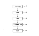
- FIG. It is a schematic longitudinal side view of the coating and developing apparatus. It is a vertical side view of a heating module provided in the coating and developing apparatus. It is a cross-sectional top view of the said heating module. It is a flowchart of the process of the wafer which concerns on 1st Embodiment. It is a schematic diagram which shows the state of a resist film. It is a schematic diagram which shows the state of a resist film. It is a schematic diagram which shows the state of a resist film. It is a schematic diagram which shows the state of a resist film. It is a schematic diagram which shows the state of a resist film. It is a schematic diagram which shows the state of a resist film.
- the coating and developing apparatus 1 for executing the resist pattern forming method according to the first embodiment of the present invention will be described.
- 1, 2, and 3 are a plan view, a perspective view, and a schematic longitudinal side view of the coating and developing apparatus 1, respectively.
- the coating and developing apparatus 1 is configured by connecting a carrier block D1, a processing block D2, and an interface block D3 in a straight line.
- An exposure device D4 is further connected to the interface block D3.
- the arrangement direction of the blocks D1 to D3 (the Y direction in FIG. 1) is the front-rear direction.
- the carrier block D1 has a role of applying a carrier C including a plurality of wafers W and carrying it in and out of the developing device 1. From the carrier C via the mounting table 11, the opening / closing part 12, and the opening / closing part 12 of the carrier C And a transfer mechanism 13 for transporting the wafer W.
- the processing block D2 is configured by laminating first to sixth unit blocks E1 to E6 for performing liquid processing on the wafer W in order from the bottom.
- “BCT” is a process for forming a lower antireflection film on the wafer W
- “COT” is a process for forming a resist film on the wafer W
- DEV is a process for forming a resist pattern on the exposed wafer W.
- a shelf unit U is provided on one of the left and right sides of the transport area 14 from the carrier block D1 to the interface block D3.
- the shelf unit U is configured, for example, by arranging six stacked heating modules stacked vertically in the front-rear direction.
- the heating modules two heating modules for performing a heat treatment on the wafer W before the development after exposure, called PEB (Post-Exposure-Bake), and 20 for performing the heat treatment on the wafer W after the development are shown. .
- PEB Post-Exposure-Bake
- the configuration of the heating module 2 will be described later.
- the heating module 20 is configured in substantially the same manner as the heating module 2 except that an infrared lamp and a filter described later are not provided.
- Each developing module 3 includes cups 31, 31 arranged in the front-rear direction, and a wafer W is placed on a chuck 32 in the cup 31.
- a nozzle (not shown) moves between the cups 31, 31, and a developer is supplied from the nozzle to the surface of the wafer W in each cup 31 to develop the resist film on the surface of the wafer W.
- a transfer arm F ⁇ b> 5 that is a transfer mechanism of the wafer W is provided.
- the transfer arm F5 can transfer the wafer W between the cup 31, the heating module 2, and a transfer module TRS provided at the height of the unit block E5 in towers T1 and T2 described later.
- the unit block E6 has the same configuration as the unit block E5.
- the unit blocks E1 and E2 have the same configuration as the unit block E5 except that an antireflection film forming module is provided instead of the developing module 3 and that the heating modules of the shelf unit U are all configured by the heating module 20. It is.
- the antireflection film forming module has the same configuration as that of the developing module 3 except that a chemical solution for forming an antireflection film is supplied from the nozzle instead of the developing solution. *
- a resist coating module is provided instead of the developing module 3.
- This resist coating module has the same configuration as the developing module 3 except that a chemically amplified and positive resist is supplied from a nozzle instead of the developer.
- the heating modules of the shelf units U of the unit blocks E3 and E4 are all configured by the heating module 20 in the first embodiment. Except for these differences, the unit blocks E3 and E4 have the same configuration as the unit block E5.
- the heating module 20 of the unit blocks E3 and E4 volatilizes and removes the solvent contained in the resist film formed on the wafer W by heating the wafer W, thereby drying the resist film. Heat treatment (Pre applied Bake: PAB) is performed.
- the transfer arms of the unit blocks E1 to E4 and E6 corresponding to the transfer arm F5 of the unit block E5 are shown as F1 to F4 and F6. *
- a tower T1 that extends vertically across the unit blocks E1 to E6 and a transfer arm 15 that is a transfer mechanism that can be moved up and down to transfer the wafer W to the tower T1. And are provided.
- the tower T1 is composed of a plurality of modules stacked on each other, and the modules provided at the heights of the unit blocks E1 to E6 are wafers between the transfer arms F1 to F6 of the unit blocks E1 to E6. W can be handed over.
- a delivery module TRS provided at the height position of each unit block
- a temperature adjustment module for adjusting the temperature of the wafer W
- a buffer module for temporarily storing a plurality of wafers W
- a hydrophobic processing module for hydrophobizing the surface of the wafer W is included.
- the hydrophobic treatment module, the temperature control module, and the buffer module are not shown.
- the interface block D3 includes towers T2, T3, and T4 extending vertically across the unit blocks E1 to E6.
- the interface block D3 is a transfer mechanism that can be moved up and down to transfer the wafer W to and from the tower T2 and the tower T3.
- An interface arm 18 is provided.
- the tower T2 includes a delivery module TRS, a buffer module for storing and retaining a plurality of wafers W before exposure processing, a buffer module for storing a plurality of wafers W after exposure processing, and a temperature for adjusting the temperature of the wafers W.
- a delivery module TRS a delivery module for storing and retaining a plurality of wafers W before exposure processing
- a buffer module for storing a plurality of wafers W after exposure processing
- a temperature for adjusting the temperature of the wafers W is stacked on each other, illustration of the buffer module and the temperature adjustment module is omitted here.
- a place where the wafer W is placed is described as a module.
- the towers T3 and T4 are also provided with modules, but the description thereof is omitted here.
- the exposure apparatus D4 exposes the resist film on the wafer W through a mask in which openings are formed along a predetermined pattern.
- reference numeral 21 denotes a housing, which is provided with a transfer port 22 for the wafer W so as to face the transfer region 14.
- reference numeral 23 denotes a shutter that opens and closes the transport port 22.
- reference numeral 24 denotes a horizontal cooling plate, which is configured to be capable of moving forward and backward with respect to the transport port 22 in the housing 21 by a driving mechanism (not shown).
- a cooling water passage (not shown) is formed in the cooling plate 24, and the wafer W placed on the cooling plate 24 is cooled after the heat treatment.
- the wafer W is transferred between the cooling plate 24 and the transfer arm F5 (F6) by the raising / lowering operation of the transfer arm F5 (F6).
- a hot plate (heating plate) 25 on which the wafer W is placed is provided on the inner side of the housing 21.
- reference numeral 26 denotes a heater for heating the hot plate 25.
- the wafer W is transferred from the cooling plate 24 to the hot plate 25 heated to a predetermined temperature and subjected to heat treatment.
- the hot plate 25 constitutes a second heating source.
- reference numeral 27 denotes an elevating pin, which is moved up and down by an elevating mechanism 28 and delivers the wafer W between the hot plate 25 and the cooling plate 24 moved onto the hot plate 25.
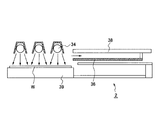
- a plurality of infrared lamps 34 which are infrared irradiation units, are provided.
- the infrared lamp 34 is configured to irradiate the wafer W with infrared rays, that is, light with a wavelength of 0.75 ⁇ m to 1 mm.
- reference numeral 35 denotes a cover that covers the side periphery and the upper side of the infrared lamp 34, and the inner peripheral surface reflects the infrared rays from the infrared lamp 34 to irradiate downward.
- a filter 36 is provided below the infrared lamp 34.
- the filter 36 is configured by, for example, laminating a plate-like glass and a film made of antimony-doped tin oxide, and is formed so as to cover the entire wafer W placed on the hot plate 24.
- the infrared rays irradiated from the infrared lamp 34 toward the wafer W transmit infrared rays having a wavelength of 2.0 ⁇ m to 6.0 ⁇ m, and block infrared rays having wavelengths other than 2.0 ⁇ m to 6.0 ⁇ m.
- the filter 36 is configured. The reason why the wafer W can be selectively irradiated with infrared rays having a wavelength of 2.0 ⁇ m to 6.0 ⁇ m will be described later.
- the filter 36 and the infrared lamp 34 constitute a first heating source.
- the coating / developing apparatus 1 is provided with a control unit 10 composed of a computer.
- the control unit 10 has a program storage unit (not shown).
- a program made of software for example, in which instructions are set so as to perform coating and developing processing, which will be described later, is stored.
- the control unit 10 outputs a control signal to each part of the coating / developing apparatus 1, and operates each transfer arm, wafer processing in each module, developer and resist on the wafer.
- the supply and the like of the wafer W can be controlled to apply and develop the wafer W as will be described later.
- This program is stored in the program storage unit while being stored in a storage medium such as a hard disk, a compact disk, a magnetic optical disk, or a memory card.
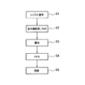
- FIG. 6 is a flowchart showing an outline of the processing steps for the wafer W of the system including the coating, developing device 1 and exposure device D4.
- the transport path of the wafer W in the coating and developing apparatus 1 will be described with reference to FIG. 6 and FIGS. 1 and 3 described above.
- the wafer W is transferred from the carrier C by the transfer mechanism 13 to the transfer module TRS0 of the tower T1 in the processing block D2.
- the wafer W is transferred from the delivery module TRS0 to the unit blocks E1 and E2 and transferred.
- the transfer module TRS1 corresponding to the unit block E1 the transfer module capable of transferring the wafer W by the transfer arm F1.
- the wafer W is transferred from the TRS0.
- the wafer W is transferred to the unit block E2
- the wafer W is transferred from the TRS0 to the transfer module TRS2 corresponding to the unit block E2 among the transfer modules TRS of the tower T1. Delivery of these wafers W is performed by the delivery arm 15.
- the wafer W thus distributed is transferred in the order of TRS1 (TRS2) ⁇ antireflection film forming module ⁇ heating module 20 ⁇ TRS1 (TRS2), and then transferred to the transfer module TRS3 corresponding to the unit block E3 by the transfer arm 15.
- TRS1 TRS2
- TRS1 TRS2
- TRS3 transfer module corresponding to the unit block E3
- TRS4 delivery module
- the wafer W thus distributed to TRS3 and TRS4 is transported from TRS3 (TRS4) to the resist coating module, and a resist is coated on the antireflection film to form a resist film on the surface of the wafer W (FIG. 6, step S1). Thereafter, the wafer W is transferred to the heating module 20, placed on the hot plate 25 of the heating module 20, and subjected to the heat treatment (PAB) (step S2), and then to the transfer module TRS of the tower T2. Be transported.
- the wafer W transferred to the delivery module TRS is carried into the exposure apparatus D4 by the interface arms 16 and 18 through the tower T3, the resist film is exposed, and a latent image of the resist pattern is formed (step S3). ).
- the wafer W is transferred between the towers T2 and T4 by the interface arms 16 and 17, and transferred to the transfer modules TRS5 and TRS6 of the tower T2 corresponding to the unit blocks E5 and E6, respectively. Thereafter, the wafer W is transferred to the heating module 2 and receives infrared irradiation and heat treatment (PEB) (step S4). Details of the processing in step S4 will be described later. Thereafter, the wafer W is transferred to the development module 3 and subjected to development processing (step S5), and a resist pattern is formed on the resist film. Thereafter, after being heated by the heating module 20, it is transported to the delivery module TRS of the tower T 1 and returned to the carrier C through the transfer mechanism 13.
- PEB infrared irradiation and heat treatment
- FIG. 7 shows the wafer W to be exposed in step S3.
- reference numeral 41 denotes a resist film.
- Reference numeral 42 denotes a resin insoluble in the developer in the resist film 41.
- reference numeral 43 denotes a mask of the exposure apparatus D4, and an opening 44 is formed in the mask 43 along a predetermined pattern. In the drawing, a portion of the mask 43 that shields light is shown as a shielding portion 45.
- an acid 47 is generated from an acid generator (not shown) contained in the resist film 41.
- the resin 42 is decomposed. Specifically, a protecting group (indicated by R in FIG. 7) for making the resin 42 insoluble in the developer is removed from the resin 42, and instead the resin 42 is changed to have a hydroxyl group. It becomes soluble in the developer.
- the resin solubilized in the developer is designated as 48 in FIG. Thus, a latent image of the pattern is formed in the resist film 41.
- a light shielding area (non-exposure area) 52 an area where light is shielded by the shielding portion 45 of the mask 43 is referred to as a light shielding area (non-exposure area) 52.
- a region (for convenience, an intermediate region) 53 is formed in which the proportion of the soluble resin 48 is larger than the light shielding region 52 and smaller than the exposure region 51.
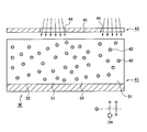
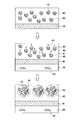
- FIG. 13 is a schematic view of the wafer W after the PEB is performed.
- a relatively large amount of acid 47 is generated before PEB is performed, and thus a change from the resin 42 to the resin 48 occurs. Therefore, after the PEB is completed, the ratio of the resin 48 is high. .
- FIG. 14 shows the wafer W after the development processing. As shown in FIG. 14, convex portions and concave portions are formed on the side walls of the resist pattern 54 from the resins 42 and 48, respectively, and the side walls of the resist pattern 54 are roughened. Becomes larger.
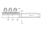
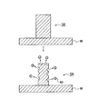
- the exposed wafer W is carried into the heating module 2, transferred from the cooling plate 24 to the hot plate 25 heated to, for example, 90 ° C. to 130 ° C., and placed thereon, and at the same time Infrared rays are irradiated from the lamp 34, and infrared rays having a wavelength of 2.0 ⁇ m to 6.0 ⁇ m are transmitted through the filter 36 and supplied to the resist film 41.
- FIG. 15 shows the heating module 2 that heats the wafer W and irradiates infrared rays in this way.
- the resin 42 stretching vibration about a single bond formed between carbon and hydrogen is promoted by the infrared ray (IR) having a wavelength of 2.0 ⁇ m to 6.0 ⁇ m.
- the stretching vibration of a single bond between carbon and hydrogen and the stretching vibration of a bond between hydrogen and oxygen in a hydroxyl group are promoted. That is, the molecules constituting the resins 42 and 48 vibrate (FIG. 9).
- the present inventor considers that the acid 47 in the exposure region 51 and the intermediate region 53 flows in the resist film 41 due to the vibration of the molecules. The flowing acid 47 acts on the resin 42, and the resin 42 changes to the resin 48. Thereby, in the exposure area 51 and the intermediate area 53, the ratio of the resin 48 to the resin 42 increases (FIG. 10).
- FIG. 11 shows the wafer W when the PEB is thus finished and unloaded from the heating module 2.
- the reason why the wavelength of the infrared ray irradiated to the wafer W is selected by the filter 36 as described above is to cause the change from the resin 42 to the resin 48 while suppressing the temperature rise of the resist film 41 due to the infrared ray. . That is, the wider the range of the wavelength of the infrared rays irradiated to the wafer W, the more easily the infrared rays that are absorbed by the resist film 41 and the silicon constituting the wafer W are included in the irradiated infrared rays. The temperature of W rises rapidly. However, when the temperature of the wafer W is rapidly increased in this way, the acid 47 is sufficiently volatilized before flowing in the resist film 41, so that the change to the resin 48 is not sufficiently performed. In order to prevent this, the above wavelength is selected.
- the acid 47 is caused to flow by the above infrared irradiation, the mixing of the resins 42 and 48 in the intermediate region 53 is prevented after the PEB is completed. Accordingly, since the entire intermediate region 53 is dissolved by the developing solution during the development processing in step S5, it is possible to prevent the sidewall region of the resist pattern 54 from being uneven from the intermediate region 53. Therefore, as shown in FIG. 12, the roughness on the side wall of the resist pattern 54 is suppressed.
- the resist film that has been exposed as described above is selectively irradiated with infrared rays having a wavelength that vibrates the molecules that constitute the resist film, and then subjected to PEB.
- the degree of roughness on the side wall of the resist pattern 54 can be suppressed.
- the flow of the acid 47 in the exposure region 51 is caused by infrared irradiation, so that the resist film 41 in the exposure region 51 after PEB is produced even if the amount of the acid 47 generated by the exposure in the exposure apparatus D4 is small.
- This resin can be made soluble in the developer.
- the resist pattern 54 can be resolved even if the intensity of light supplied to the wafer W is suppressed in the exposure apparatus D4.
- the exposure apparatus D4 an apparatus using KrF or ArF as a light source may be used.
- the wafer W is placed on the hot plate 25, and the wafer W is irradiated with infrared rays while raising the temperature, thereby improving the throughput.
- the wafer W placed on the cooling plate 24 positioned below the filter 36 is irradiated with infrared rays, and then the wafer W is placed on the hot plate 25 to perform PEB. May be.
- infrared irradiation may be continued on the wafer W, or after transferring the wafer W to the hot plate 25, the infrared irradiation may be stopped. .
- infrared irradiation is started from a state where the cooling plate 24 is positioned away from the hot plate 25 on the near side of the module 2 as shown by a chain line in the figure, and the hot plate 25 is shown as shown by a solid line in the figure. Infrared irradiation is performed until it is positioned above. That is, infrared irradiation may be performed while the wafer W is being transferred to the hot plate 25 by the cooling plate 24 that is a moving unit.
- a driving unit 38 that moves the filter 36 toward the front side in the housing 21 in the heating module 2 may be provided.
- a stage 39 not provided with the heater 26 is provided instead of the hot plate 25, for example.
- the wafer W placed on the stage 39 is irradiated with infrared rays through a filter 36 disposed on the stage 39 to cause the acid to flow.
- the filter 36 is withdrawn from the stage 39, and the wafer W is irradiated with infrared rays having a wavelength in a range wider than 2.0 ⁇ m to 6.0 ⁇ m from the infrared lamp 34 to perform PEB. May be.
- the filter 36 that is retracted from the stage 39 and located at a position off the optical path from the infrared lamp 34 to the wafer W, and the infrared lamp 34 constitute a second heating source.
- the stage 39 and the infrared lamp 34 may be moved, and the PEB may be performed after flowing the acid.
- the heating module 2 is provided as a heating module of the unit blocks E3 and E4. Further, for example, the heating module of the unit blocks E5 and E6 includes the heating module 20 in which the filter 36 and the infrared lamp 34 are not provided.
- FIG. 18 is a flowchart in the second embodiment.
- step S2 is different from the first embodiment, and the wafer W is irradiated with infrared rays when performing PAB.
- the wafer W is placed on the heated hot plate 25, and the wafer W placed on the hot plate 25 is placed on the hot plate 25 through a filter 36 to 2.0 ⁇ m to Irradiate 6.0 ⁇ m infrared rays. That is, infrared irradiation is performed while the wafer W is placed on the hot plate 25 and heated to remove the solvent of the resist film. In this example, infrared irradiation is not performed in step S4.
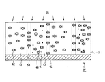
- FIG. 19 a schematic diagram of a resist film 41 in the case of performing PAB without performing infrared irradiation is shown in the schematic diagram.
- the resin 42 in the resist film 41 is shown in a shape different from that in FIGS.
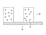
- the upper part of FIG. 19 shows the resist film 41 before performing PAB, and shows resist particles 40 formed by collecting the resins 42 in the resist film 41. Prior to PAB, the particles 40 are dispersed in the resist film 41 with relatively high uniformity.
- the middle part of FIG. 19 shows a state where the wafer W is placed on the hot plate 25 and PAB is performed.
- the wafer W is heated by the hot plate 25 from the lower side, whereby a temperature gradient is formed in the resist film 41. Since the solvent remains in the resist film 41 during the PAB, the fluidity of the particles 40 is relatively high, so that the particles 40 flow according to the temperature gradient. It is considered that a plurality of particles 40 are aggregated during this flow, and the particle size of the particles 40 is increased as shown in the lower part of FIG.
- the resist pattern 54 having a target shape.
- the resist pattern is aimed to be formed in a rectangular shape when viewed from the side, but is actually supplied to wash away the developer flowing on the surface of the wafer W and the developer from the wafer W after the developer is supplied.
- the upper and side surfaces of the cleaning liquid are scraped off.
- the diameter of the particle 40 is large as described above, the diameter of the particle 40 that is scraped away from the resist pattern 54 as shown in the lower part of FIG.
- the diameter of the particles 40 detached from the upper part of the resist pattern 54 is large, it is considered that the difference between the height of the resist pattern 54 and the film thickness of the resist film 41 at the end of PAB is increased.
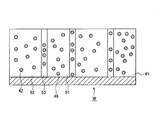
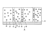
- the upper part of FIG. 21 shows the wafer W before performing PAB as in the upper part of FIG.
- the resist particles 40 are dispersed in the resist film 41 with high uniformity.
- the wafer W is placed on the hot plate 25 and irradiated with infrared rays having a wavelength of 2.0 ⁇ m to 6.0 ⁇ m while performing PAB. It shows the state.
- the infrared rays are absorbed by the resin 42, and the stretching vibration of the interatomic bond of the resin 42 is promoted as described in the first embodiment. Infrared rays enter the deep portion from the surface layer of the resist film 41, and the resin 42 vibrates throughout the resist film 41, and the resist film 41 generates heat due to this vibration. The inventor believes that this heat generation suppresses the temperature gradient in the resist film 41 formed by the hot plate 25 and suppresses the flow of the particles 40. As a result, as shown in the lower part of FIG. 21, the present inventor believes that the particles 40 are dispersed with high uniformity in the resist film 41 even after the PAB is completed, and aggregation is suppressed.
- the diameter of the particles 40 that are shaved and detached becomes small. Therefore, the unevenness of the sidewall of the resist pattern 54 is suppressed from increasing. That is, the roughness of the side wall is suppressed. Further, it is possible to suppress the height of the resist pattern 54 from becoming smaller than the film thickness of the resist film 41 after the PAB is completed.
- the first embodiment and the second embodiment may be combined with each other. That is, the wafer W may be irradiated with infrared light having the above wavelength when performing PAB, and the wafer W may be exposed and then irradiated with infrared light having the above wavelength to perform PEB.
- the wafer W is not limited to being heated by the hot plate 25 including the heater 26 as described above.
- the heating module 2 is configured to include LEDs that irradiate light on the back surface of the wafer W. The wafer W may be heated by irradiating light of a wavelength absorbed by silicon constituting the wafer W from this LED.
- the resist a positive resist has been described, but a negative resist may be used.
- the use of a chemically amplified resist is not limited in order to prevent pattern roughness by suppressing particle aggregation as described above. That is, a resist that does not contain an acid generator may be used.
- the module for performing infrared irradiation and the module for performing PEB are configured as the heating module 2 in order to save the module space, but the module for performing infrared irradiation is used. And a module for performing PEB may be provided separately.
- one of the modules of the shelf units U of the unit blocks E5 and E6 is configured as an infrared irradiation module including the stage 39, the filter 36, and the infrared lamp 34, and the infrared radiation is applied to the wafer W by the infrared module. Then, the wafer W may be transferred to the heating module 20 of the shelf unit U and PEB may be performed on the wafer W.
- Evaluation test A plurality of wafers W were processed according to the procedure shown in the first embodiment. Processing is performed by changing the dose amount (mJ / cm 2 ) which is the energy amount of the exposure beam in the exposure apparatus D4 for each wafer W, and the resist pattern 54 has a line width CD (nm) and the side wall of the resist pattern 54.
- LWR Line Width Roughness (nm), which is an index of roughness, was measured.
- the Dose amount is changed by 1 mJ / cm 2 increments, respectively 20.5mJ / cm 2 and Dose amount, 19.5mJ / cm 2, 18.5mJ / cm 2, 17.5mJ / cm 2, what was 16.5mJ / cm 2 They are described as evaluation tests 1-1, 1-2, 1-3, 1-4, and 1-5.
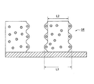
- the LWR is the maximum value-minimum value of the line width of the resist pattern 54, and is the difference between L1 and L2 in the figure when the resist pattern 54 is formed as shown in FIG. The smaller the LWR value, the less the roughness of the side wall of the resist pattern 54, which is preferable.
- infrared irradiation with a wavelength as described above and PEB were performed in different modules, and the wafer W was placed on a cooling plate and the temperature was adjusted to 35 ° C. during infrared irradiation.
- the PEB was performed by placing the wafer W on the hot plate 25, and the wafer W was not irradiated with infrared rays while being placed on the hot plate 25.
- the CD and LWR were measured in the same manner as in the evaluation tests 1-1 to 1-5 except that infrared irradiation was not performed. In this control test, the dose was set to 21.5 mJ / cm 2 .
- Table 1 below shows the results of this evaluation test 1.
- the dose amount is smaller than the dose amount in the control test, but the LWR and CD are the same as or higher than those in the control test. It was confirmed that it was getting smaller.
- evaluation tests 1-1 to 1-5 it was confirmed that the larger the dose amount, the smaller the CD. Therefore, from the result of this evaluation test 1, by performing the processing according to the first embodiment, the resist pattern 4 is prevented from being roughened and irradiated with the exposure apparatus D4 to obtain a CD having a predetermined line width. It was confirmed that the exposure energy can be suppressed.
- evaluation test 2 a process similar to that of the second embodiment was performed as an evaluation test 2-1. That is, when performing PAB, the wafer W was irradiated with infrared light, and thereafter, the resist pattern 54 was formed on the wafer W without performing infrared irradiation.
- evaluation test 2-2 PAB was performed by the same procedure as the evaluation test 2-1, and the resist pattern 54 was formed. After the exposure, the wafer W was irradiated with infrared rays and the wafer W was irradiated as in the first embodiment. The PEB was performed by heating.
- evaluation test 2-3 as in evaluation test 1, the wafer W on the cooling plate was irradiated with infrared rays, and then the wafer W was placed on the hot plate 25 and subjected to PEB, whereby a resist pattern 54 was formed on the wafer W. .
- infrared irradiation is not performed when PAB is performed.
- the infrared irradiation was performed for a longer time than the evaluation test 2-2, specifically, for 3 minutes. The cross section of the resist pattern 54 formed in the evaluation tests 2-1 to 2-3 was observed, and the height thereof was measured.
- a resist pattern 54 was formed without irradiating the wafer W with infrared rays after applying the resist and performing PEB. Also in this control test, the cross section of the resist pattern 54 was observed and the height thereof was measured as in the evaluation tests 2-1 to 2-3.
- FIG. 23 to 26 show resist patterns 54 of the control test and the evaluation tests 2-1 to 2-3.
- Each figure shows a schematic diagram of the resist pattern 54 viewed from the upper side on the upper side and the resist pattern 54 on the lower side.
- 54 is a schematic diagram of a cross section of each of 54.
- the height H1 of the resist pattern 54 was 60 nm in the control test, 80 nm in the evaluation test 2-1 and evaluation test 2-2, and 50 nm in the evaluation test 2-3.
- the height of the resist pattern 54 is larger than that of the control test because the particles 40 in the resist film 41 are irradiated by infrared rays irradiated during PAB as described in the second embodiment.
- evaluation test 3 As an evaluation test 3, a process was performed in accordance with the first embodiment, and in order to perform PEB, the wafer W being heated was irradiated with infrared rays to form a resist pattern. For each wafer W, the infrared irradiation time was changed in the range of 40 to 80 seconds. In this evaluation test 3, an apparatus using ArF as a light source was used as the exposure apparatus D4, and it was set to form a 45 nm pattern on the resist. Further, as a control test, the wafer W was processed without being irradiated with infrared rays after exposure to form a resist pattern. The time for placing the wafer W on the hot plate 25 when performing PEB was 60 seconds. In the evaluation test 3 and the control test, the LWR of the resist pattern at various locations on the wafer W was measured. Moreover, the average was calculated about measured LWR.
- Table 2 below shows the results of the evaluation test 3.
- the infrared irradiation time is 60 seconds, 70 seconds, and 80 seconds, respectively, the average value of LWR is smaller than that of the control test. Therefore, this evaluation test 3 shows that the LWR can be reduced by the method of the first embodiment, that is, the roughness of the resist pattern 54 can be suppressed.
- evaluation Test 4 As an evaluation test 4, a process was performed according to the second embodiment, and a resist pattern 54 was formed on the wafer W. That is, when performing PAB, the wafer W was irradiated with infrared rays having a wavelength of 2.0 ⁇ m to 6.0 ⁇ m. After the exposure, the wafer W is not irradiated with the infrared rays. In this evaluation test 4, for each wafer W, the infrared irradiation time was changed in the range of 50 to 70 seconds. Further, a resist pattern was formed on the wafer W in the same manner as in the evaluation test 4 except that the infrared irradiation was not performed when the PAB was performed as a control test.
- the wafer W is not irradiated with infrared rays until the resist pattern is formed after the resist application.
- the heating time of the wafer W was 60 seconds.
- the CD and LWR of the resist pattern were measured.
- Table 3 below shows the results of Evaluation Test 4.
- the irradiation time of infrared rays is 50 seconds
- the average value of LWR is larger than that of the control test, but when the irradiation time is 60 seconds and 70 seconds, the average value of LWR is smaller than that of the control test. Therefore, from the result of the evaluation test 4, it was shown that the LWR can be improved by using the method of the second embodiment.
- CD became small as infrared irradiation time became long.
- evaluation Test 5 As the evaluation test 5, the treatment was performed in substantially the same procedure as the evaluation test 4. As a difference from the evaluation test 4, similarly to the first embodiment, the wafer W was irradiated with infrared rays having a wavelength in the above range even when performing PEB. The infrared irradiation time during the PEB treatment was set to 60 seconds. The infrared irradiation time for performing the PAB was changed for each wafer W in the same manner as in the evaluation test 4. As in the evaluation test 4, for each wafer W, the infrared irradiation time during PAB was changed in the range of 50 to 70 seconds.
- the results of evaluation test 5 are shown in Table 4 below. In the table, the results of the control test described in Evaluation Test 4 are also shown.
- the irradiation time of infrared rays in PAB is 50 seconds
- the average value of LWR is larger than that of the control test, but when the irradiation time is 60 seconds and 70 seconds, the average value of LWR is smaller than that of the control test. Therefore, from the result of the evaluation test 5, it was shown that the LWR can be improved even when the methods of the first and second embodiments are combined.
- CD became small as infrared irradiation time at the time of performing PAB became long.
- evaluation Test 6 As the evaluation test 6, as in the evaluation test 1, the exposed wafer W placed on the cooling plate is irradiated with infrared rays, and then the wafer W is transferred to the hot plate 25 and PEB is performed to form a resist pattern 54. did. The irradiation time of the infrared rays was changed in the range of 60 seconds to 300 seconds for each wafer W. The heating time by the hot plate 25 was 60 seconds. In the same manner as in Evaluation Tests 3 to 5, the formed resist patterns were measured for LWR at various locations on the wafer W, and the average value was calculated. Further, the CD of this resist pattern was measured.
- Table 5 shows the results of the evaluation test 6.
- the results of the control test described in Evaluation Test 4 are also shown.
- the irradiation time of infrared rays is 300 seconds, the average value of LWR is large with respect to the control test, but when the irradiation time is 60 seconds and 180 seconds, the average value of LWR is small with respect to the control test. Therefore, from the result of the evaluation test 6, it was shown that the roughness of the resist pattern 54 can be suppressed by irradiating the wafer W after exposure with infrared rays for an appropriate time.
- the irradiation may be performed during the heating of the wafer W or before the heat treatment.
- evaluation Test 7 As the evaluation test 7, similarly to the evaluation test 3, the wafer W after exposure was irradiated with infrared rays having the above-described wavelength during heating to form a resist pattern 54. The infrared irradiation time was changed every 10 seconds in the range of 40 to 70 seconds for each wafer W.
- an apparatus using KrF as a light source was used as the exposure apparatus D4, and a resist developed for EUV exposure was used as the resist. Further, in this evaluation test 7, exposure processing was performed at different locations on the same wafer W while changing the dose amount.
- the dose amount (the appropriate dose amount) at which the CD of the resist pattern 54 becomes a target value was examined.
- the wafer W was processed in the same manner as in the evaluation test 7 except that the infrared ray was not irradiated to form a resist pattern 54. Then, the CD, LWR, and appropriate dose amount were examined as in the evaluation test 7.
- Table 6 below shows the results of the evaluation test 7.
- Table 6 shows the appropriate dose amount, the sensitivity improvement rate, the average value of LWR, and the minimum value of LWR are shown for each irradiation time of infrared rays. Show.
- the sensitivity improvement rate is (ZY) / Y ⁇ 100, where Y is the appropriate dose amount when the irradiation time is X, and Z is the appropriate dose amount of the control test.
- the results of the evaluation test 7 are also shown in the graphs of FIGS. In the graph of FIG. 27, the vertical axis represents the measured CD, and the horizontal axis represents the dose amount during exposure. In the graph of FIG. 28, the vertical axis indicates the average value of LWR, and the horizontal axis indicates the dose amount.
- the sensitivity improvement rate is high when the irradiation time is 50 seconds, 60 seconds, and 70 seconds, and the average value and the minimum value of LWR are small compared to the control test. . Therefore, from this evaluation test 7, it was shown that the LWR can be improved by the method of the first embodiment and the sensitivity of the resist film with respect to the exposure amount can be improved.
Landscapes
- Physics & Mathematics (AREA)
- General Physics & Mathematics (AREA)
- Electromagnetism (AREA)
- Photosensitive Polymer And Photoresist Processing (AREA)
- Exposure Of Semiconductors, Excluding Electron Or Ion Beam Exposure (AREA)
Priority Applications (1)
| Application Number | Priority Date | Filing Date | Title |
|---|---|---|---|
| US14/889,564 US10459339B2 (en) | 2013-05-10 | 2014-05-08 | Resist pattern forming method, coating and developing apparatus and storage medium |
Applications Claiming Priority (2)
| Application Number | Priority Date | Filing Date | Title |
|---|---|---|---|
| JP2013-100693 | 2013-05-10 | ||
| JP2013100693A JP6020344B2 (ja) | 2013-05-10 | 2013-05-10 | レジストパターン形成方法、塗布、現像装置、記憶媒体 |
Publications (1)
| Publication Number | Publication Date |
|---|---|
| WO2014181837A1 true WO2014181837A1 (ja) | 2014-11-13 |
Family
ID=51867314
Family Applications (1)
| Application Number | Title | Priority Date | Filing Date |
|---|---|---|---|
| PCT/JP2014/062384 Ceased WO2014181837A1 (ja) | 2013-05-10 | 2014-05-08 | レジストパターン形成方法、塗布、現像装置及び記憶媒体 |
Country Status (4)
| Country | Link |
|---|---|
| US (1) | US10459339B2 (https=) |
| JP (1) | JP6020344B2 (https=) |
| TW (1) | TWI607490B (https=) |
| WO (1) | WO2014181837A1 (https=) |
Families Citing this family (4)
| Publication number | Priority date | Publication date | Assignee | Title |
|---|---|---|---|---|
| JP7124277B2 (ja) * | 2016-12-13 | 2022-08-24 | 東京エレクトロン株式会社 | 光処理装置及び基板処理装置 |
| KR102513167B1 (ko) * | 2018-06-15 | 2023-03-23 | 매슨 테크놀로지 인크 | 워크피스의 노광 후 베이크 공정을 위한 방법 및 장치 |
| UY38361A (es) | 2018-09-04 | 2020-03-31 | Univ La Republica | Bacterias modificadas genéticamente para la producción de tres enzimas de reparación de adn y método para evaluar la actividad de reparación de adn |
| US20230152705A1 (en) * | 2021-11-17 | 2023-05-18 | Tokyo Electron Limited | UV Treatment of EUV Resists |
Citations (7)
| Publication number | Priority date | Publication date | Assignee | Title |
|---|---|---|---|---|
| JPH07297096A (ja) * | 1994-04-22 | 1995-11-10 | Nec Corp | 露光方法およびその装置 |
| JP2004327688A (ja) * | 2003-04-24 | 2004-11-18 | Nippon Telegr & Teleph Corp <Ntt> | レジスト現像方法及びレジスト現像装置 |
| JP2008159768A (ja) * | 2006-12-22 | 2008-07-10 | Tokyo Electron Ltd | ベーキング装置及び基板処理装置 |
| JP2011099956A (ja) * | 2009-11-05 | 2011-05-19 | Toppan Printing Co Ltd | レジストのベーク方法及びベーク装置 |
| JP2011165693A (ja) * | 2010-02-04 | 2011-08-25 | Tokyo Electron Ltd | 熱処理装置、塗布現像処理システム、熱処理方法、塗布現像処理方法及びその熱処理方法又は塗布現像処理方法を実行させるためのプログラムを記録した記録媒体 |
| JP2011204774A (ja) * | 2010-03-24 | 2011-10-13 | Toshiba Corp | パターン形成方法および脱水装置 |
| JP2013069962A (ja) * | 2011-09-26 | 2013-04-18 | Dainippon Screen Mfg Co Ltd | 熱処理方法および熱処理装置 |
Family Cites Families (4)
| Publication number | Priority date | Publication date | Assignee | Title |
|---|---|---|---|---|
| JPH02230252A (ja) * | 1989-03-03 | 1990-09-12 | Nec Corp | パターン形成方法 |
| JP4788610B2 (ja) | 2007-01-17 | 2011-10-05 | 東京エレクトロン株式会社 | 加熱装置、塗布、現像装置、加熱方法及び記憶媒体 |
| JP5290129B2 (ja) * | 2008-12-25 | 2013-09-18 | 信越化学工業株式会社 | 化学増幅ポジ型レジスト組成物及びレジストパターン形成方法 |
| JP4853536B2 (ja) * | 2009-03-13 | 2012-01-11 | 東京エレクトロン株式会社 | 塗布、現像装置、塗布、現像方法及び記憶媒体 |
-
2013
- 2013-05-10 JP JP2013100693A patent/JP6020344B2/ja active Active
-
2014
- 2014-05-02 TW TW103115809A patent/TWI607490B/zh active
- 2014-05-08 WO PCT/JP2014/062384 patent/WO2014181837A1/ja not_active Ceased
- 2014-05-08 US US14/889,564 patent/US10459339B2/en active Active
Patent Citations (7)
| Publication number | Priority date | Publication date | Assignee | Title |
|---|---|---|---|---|
| JPH07297096A (ja) * | 1994-04-22 | 1995-11-10 | Nec Corp | 露光方法およびその装置 |
| JP2004327688A (ja) * | 2003-04-24 | 2004-11-18 | Nippon Telegr & Teleph Corp <Ntt> | レジスト現像方法及びレジスト現像装置 |
| JP2008159768A (ja) * | 2006-12-22 | 2008-07-10 | Tokyo Electron Ltd | ベーキング装置及び基板処理装置 |
| JP2011099956A (ja) * | 2009-11-05 | 2011-05-19 | Toppan Printing Co Ltd | レジストのベーク方法及びベーク装置 |
| JP2011165693A (ja) * | 2010-02-04 | 2011-08-25 | Tokyo Electron Ltd | 熱処理装置、塗布現像処理システム、熱処理方法、塗布現像処理方法及びその熱処理方法又は塗布現像処理方法を実行させるためのプログラムを記録した記録媒体 |
| JP2011204774A (ja) * | 2010-03-24 | 2011-10-13 | Toshiba Corp | パターン形成方法および脱水装置 |
| JP2013069962A (ja) * | 2011-09-26 | 2013-04-18 | Dainippon Screen Mfg Co Ltd | 熱処理方法および熱処理装置 |
Also Published As
| Publication number | Publication date |
|---|---|
| US20160085154A1 (en) | 2016-03-24 |
| TW201515061A (zh) | 2015-04-16 |
| JP2014220471A (ja) | 2014-11-20 |
| US10459339B2 (en) | 2019-10-29 |
| JP6020344B2 (ja) | 2016-11-02 |
| TWI607490B (zh) | 2017-12-01 |
Similar Documents
| Publication | Publication Date | Title |
|---|---|---|
| KR101207046B1 (ko) | 기판 처리 방법, 컴퓨터 판독 가능한 기억 매체 및 기판 처리 시스템 | |
| JP4975790B2 (ja) | レジスト液供給装置、レジスト液供給方法、プログラム及びコンピュータ記憶媒体 | |
| TWI820009B (zh) | 光處理裝置及基板處理裝置 | |
| JP7127714B2 (ja) | 露光装置及び露光方法 | |
| JP6020344B2 (ja) | レジストパターン形成方法、塗布、現像装置、記憶媒体 | |
| JP6293645B2 (ja) | 基板処理システム | |
| US20090004607A1 (en) | Substrate Processing Method | |
| TW200836244A (en) | Immersion lithography method | |
| CN102169826B (zh) | 基板处理方法 | |
| TWI881949B (zh) | 基板處理方法及基板處理系統 | |
| TWI820469B (zh) | 倍縮光罩之表面的處理方法及半導體製造系統 | |
| TW201842582A (zh) | 成膜系統、成膜方法及電腦記憶媒體 | |
| US20110143290A1 (en) | Developing treatment method and computer-readable storage medium | |
| JP2016213438A (ja) | 基板処理方法、基板処理装置及び基板処理システム | |
| US8420303B2 (en) | Substrate processing method, computer-readable storage medium and substrate processing system | |
| TW201626437A (zh) | 基板處理方法、程式、電腦記憶媒體及基板處理系統 | |
| WO2011099221A1 (ja) | 基板処理方法 | |
| JP2008004591A (ja) | 基板の処理方法、プログラム、コンピュータ読み取り可能な記録媒体及び基板の処理システム | |
| KR20090103806A (ko) | 레지스트액 공급 장치, 레지스트액 공급 방법 및 컴퓨터 판독 가능한 기억 매체 |
Legal Events
| Date | Code | Title | Description |
|---|---|---|---|
| 121 | Ep: the epo has been informed by wipo that ep was designated in this application |
Ref document number: 14794169 Country of ref document: EP Kind code of ref document: A1 |
|
| WWE | Wipo information: entry into national phase |
Ref document number: 14889564 Country of ref document: US |
|
| NENP | Non-entry into the national phase |
Ref country code: DE |
|
| 122 | Ep: pct application non-entry in european phase |
Ref document number: 14794169 Country of ref document: EP Kind code of ref document: A1 |