WO2014181792A1 - 高耐久性、高変換効率を有する色素増感型太陽電池 - Google Patents
高耐久性、高変換効率を有する色素増感型太陽電池 Download PDFInfo
- Publication number
- WO2014181792A1 WO2014181792A1 PCT/JP2014/062240 JP2014062240W WO2014181792A1 WO 2014181792 A1 WO2014181792 A1 WO 2014181792A1 JP 2014062240 W JP2014062240 W JP 2014062240W WO 2014181792 A1 WO2014181792 A1 WO 2014181792A1
- Authority
- WO
- WIPO (PCT)
- Prior art keywords
- dye
- titanium
- solar cell
- sensitized solar
- photoelectrode
- Prior art date
Links
- 238000006243 chemical reaction Methods 0.000 title abstract description 33
- 239000010936 titanium Substances 0.000 claims abstract description 144
- RTAQQCXQSZGOHL-UHFFFAOYSA-N Titanium Chemical compound [Ti] RTAQQCXQSZGOHL-UHFFFAOYSA-N 0.000 claims abstract description 139
- 229910052719 titanium Inorganic materials 0.000 claims abstract description 139
- 239000004065 semiconductor Substances 0.000 claims abstract description 45
- 239000003792 electrolyte Substances 0.000 claims abstract description 40
- 229910001069 Ti alloy Inorganic materials 0.000 claims abstract description 35
- 239000000956 alloy Substances 0.000 claims abstract description 30
- 239000003054 catalyst Substances 0.000 claims abstract description 22
- 230000009467 reduction Effects 0.000 claims abstract description 14
- 239000007769 metal material Substances 0.000 claims abstract description 8
- 239000000463 material Substances 0.000 claims description 122
- GWEVSGVZZGPLCZ-UHFFFAOYSA-N Titan oxide Chemical compound O=[Ti]=O GWEVSGVZZGPLCZ-UHFFFAOYSA-N 0.000 claims description 95
- OGIDPMRJRNCKJF-UHFFFAOYSA-N titanium oxide Inorganic materials [Ti]=O OGIDPMRJRNCKJF-UHFFFAOYSA-N 0.000 claims description 79
- 238000000034 method Methods 0.000 claims description 71
- 229910052751 metal Inorganic materials 0.000 claims description 56
- 239000002184 metal Substances 0.000 claims description 56
- 238000010438 heat treatment Methods 0.000 claims description 46
- 239000012298 atmosphere Substances 0.000 claims description 43
- NRTOMJZYCJJWKI-UHFFFAOYSA-N Titanium nitride Chemical compound [Ti]#N NRTOMJZYCJJWKI-UHFFFAOYSA-N 0.000 claims description 42
- 239000008151 electrolyte solution Substances 0.000 claims description 41
- 239000013307 optical fiber Substances 0.000 claims description 34
- BASFCYQUMIYNBI-UHFFFAOYSA-N platinum Chemical group [Pt] BASFCYQUMIYNBI-UHFFFAOYSA-N 0.000 claims description 32
- IJGRMHOSHXDMSA-UHFFFAOYSA-N Atomic nitrogen Chemical compound N#N IJGRMHOSHXDMSA-UHFFFAOYSA-N 0.000 claims description 29
- 229910001873 dinitrogen Inorganic materials 0.000 claims description 27
- 239000000758 substrate Substances 0.000 claims description 24
- 230000009471 action Effects 0.000 claims description 22
- 238000005530 etching Methods 0.000 claims description 21
- 239000003795 chemical substances by application Substances 0.000 claims description 18
- 230000001590 oxidative effect Effects 0.000 claims description 18
- QVGXLLKOCUKJST-UHFFFAOYSA-N atomic oxygen Chemical compound [O] QVGXLLKOCUKJST-UHFFFAOYSA-N 0.000 claims description 17
- 239000001301 oxygen Substances 0.000 claims description 17
- 229910052760 oxygen Inorganic materials 0.000 claims description 17
- QGZKDVFQNNGYKY-UHFFFAOYSA-N Ammonia Chemical compound N QGZKDVFQNNGYKY-UHFFFAOYSA-N 0.000 claims description 16
- 229910052697 platinum Inorganic materials 0.000 claims description 16
- 230000008569 process Effects 0.000 claims description 13
- 238000007743 anodising Methods 0.000 claims description 12
- 230000001678 irradiating effect Effects 0.000 claims description 9
- 238000004519 manufacturing process Methods 0.000 claims description 7
- 208000037998 chronic venous disease Diseases 0.000 claims description 6
- 239000007921 spray Substances 0.000 claims description 3
- 239000010408 film Substances 0.000 description 48
- 239000000975 dye Substances 0.000 description 40
- NBIIXXVUZAFLBC-UHFFFAOYSA-N Phosphoric acid Chemical compound OP(O)(O)=O NBIIXXVUZAFLBC-UHFFFAOYSA-N 0.000 description 26
- 230000005540 biological transmission Effects 0.000 description 19
- 150000007522 mineralic acids Chemical class 0.000 description 19
- 239000011521 glass Substances 0.000 description 18
- 238000004381 surface treatment Methods 0.000 description 17
- 239000002253 acid Substances 0.000 description 15
- 229910000147 aluminium phosphate Inorganic materials 0.000 description 13
- MHAJPDPJQMAIIY-UHFFFAOYSA-N Hydrogen peroxide Chemical compound OO MHAJPDPJQMAIIY-UHFFFAOYSA-N 0.000 description 12
- QAOWNCQODCNURD-UHFFFAOYSA-N Sulfuric acid Chemical compound OS(O)(=O)=O QAOWNCQODCNURD-UHFFFAOYSA-N 0.000 description 12
- 238000002048 anodisation reaction Methods 0.000 description 12
- 239000000843 powder Substances 0.000 description 12
- 150000007524 organic acids Chemical class 0.000 description 11
- 239000011347 resin Substances 0.000 description 11
- 229920005989 resin Polymers 0.000 description 11
- 125000006850 spacer group Chemical group 0.000 description 10
- WEVYAHXRMPXWCK-UHFFFAOYSA-N Acetonitrile Chemical compound CC#N WEVYAHXRMPXWCK-UHFFFAOYSA-N 0.000 description 9
- 239000007789 gas Substances 0.000 description 9
- 238000005121 nitriding Methods 0.000 description 9
- 239000003566 sealing material Substances 0.000 description 9
- 239000007864 aqueous solution Substances 0.000 description 8
- 239000003575 carbonaceous material Substances 0.000 description 8
- 239000011248 coating agent Substances 0.000 description 8
- 238000000576 coating method Methods 0.000 description 8
- 239000002904 solvent Substances 0.000 description 8
- 150000007513 acids Chemical class 0.000 description 7
- NIXOWILDQLNWCW-UHFFFAOYSA-N acrylic acid group Chemical group C(C=C)(=O)O NIXOWILDQLNWCW-UHFFFAOYSA-N 0.000 description 7
- 239000010419 fine particle Substances 0.000 description 7
- DKGAVHZHDRPRBM-UHFFFAOYSA-N Tert-Butanol Chemical compound CC(C)(C)O DKGAVHZHDRPRBM-UHFFFAOYSA-N 0.000 description 6
- 230000006872 improvement Effects 0.000 description 6
- 238000002347 injection Methods 0.000 description 6
- 239000007924 injection Substances 0.000 description 6
- HSZCZNFXUDYRKD-UHFFFAOYSA-M lithium iodide Chemical compound [Li+].[I-] HSZCZNFXUDYRKD-UHFFFAOYSA-M 0.000 description 6
- 229910044991 metal oxide Inorganic materials 0.000 description 6
- 150000004706 metal oxides Chemical class 0.000 description 6
- 235000005985 organic acids Nutrition 0.000 description 6
- 230000003647 oxidation Effects 0.000 description 6
- 238000007254 oxidation reaction Methods 0.000 description 6
- 150000003839 salts Chemical class 0.000 description 6
- 239000000243 solution Substances 0.000 description 6
- 229910019142 PO4 Inorganic materials 0.000 description 5
- KJTLSVCANCCWHF-UHFFFAOYSA-N Ruthenium Chemical compound [Ru] KJTLSVCANCCWHF-UHFFFAOYSA-N 0.000 description 5
- ATJFFYVFTNAWJD-UHFFFAOYSA-N Tin Chemical compound [Sn] ATJFFYVFTNAWJD-UHFFFAOYSA-N 0.000 description 5
- 229910052782 aluminium Inorganic materials 0.000 description 5
- XAGFODPZIPBFFR-UHFFFAOYSA-N aluminium Chemical compound [Al] XAGFODPZIPBFFR-UHFFFAOYSA-N 0.000 description 5
- 150000001875 compounds Chemical class 0.000 description 5
- 239000000835 fiber Substances 0.000 description 5
- 239000000203 mixture Substances 0.000 description 5
- 235000021317 phosphate Nutrition 0.000 description 5
- 238000005240 physical vapour deposition Methods 0.000 description 5
- 238000007789 sealing Methods 0.000 description 5
- 239000007784 solid electrolyte Substances 0.000 description 5
- ISHFYECQSXFODS-UHFFFAOYSA-M 1,2-dimethyl-3-propylimidazol-1-ium;iodide Chemical compound [I-].CCCN1C=C[N+](C)=C1C ISHFYECQSXFODS-UHFFFAOYSA-M 0.000 description 4
- 229920000178 Acrylic resin Polymers 0.000 description 4
- 239000004925 Acrylic resin Substances 0.000 description 4
- OKTJSMMVPCPJKN-UHFFFAOYSA-N Carbon Chemical compound [C] OKTJSMMVPCPJKN-UHFFFAOYSA-N 0.000 description 4
- UFHFLCQGNIYNRP-UHFFFAOYSA-N Hydrogen Chemical compound [H][H] UFHFLCQGNIYNRP-UHFFFAOYSA-N 0.000 description 4
- XUIMIQQOPSSXEZ-UHFFFAOYSA-N Silicon Chemical compound [Si] XUIMIQQOPSSXEZ-UHFFFAOYSA-N 0.000 description 4
- 238000002156 mixing Methods 0.000 description 4
- 229910052707 ruthenium Inorganic materials 0.000 description 4
- -1 salt compound Chemical class 0.000 description 4
- 229910052710 silicon Inorganic materials 0.000 description 4
- 239000010703 silicon Substances 0.000 description 4
- 238000005507 spraying Methods 0.000 description 4
- ZCYVEMRRCGMTRW-UHFFFAOYSA-N 7553-56-2 Chemical compound [I] ZCYVEMRRCGMTRW-UHFFFAOYSA-N 0.000 description 3
- QTBSBXVTEAMEQO-UHFFFAOYSA-N Acetic acid Chemical compound CC(O)=O QTBSBXVTEAMEQO-UHFFFAOYSA-N 0.000 description 3
- MYMOFIZGZYHOMD-UHFFFAOYSA-N Dioxygen Chemical compound O=O MYMOFIZGZYHOMD-UHFFFAOYSA-N 0.000 description 3
- MUBZPKHOEPUJKR-UHFFFAOYSA-N Oxalic acid Chemical compound OC(=O)C(O)=O MUBZPKHOEPUJKR-UHFFFAOYSA-N 0.000 description 3
- BQCADISMDOOEFD-UHFFFAOYSA-N Silver Chemical compound [Ag] BQCADISMDOOEFD-UHFFFAOYSA-N 0.000 description 3
- QCWXUUIWCKQGHC-UHFFFAOYSA-N Zirconium Chemical compound [Zr] QCWXUUIWCKQGHC-UHFFFAOYSA-N 0.000 description 3
- 229910052799 carbon Inorganic materials 0.000 description 3
- KRKNYBCHXYNGOX-UHFFFAOYSA-N citric acid Chemical compound OC(=O)CC(O)(C(O)=O)CC(O)=O KRKNYBCHXYNGOX-UHFFFAOYSA-N 0.000 description 3
- 238000000151 deposition Methods 0.000 description 3
- 229910001882 dioxygen Inorganic materials 0.000 description 3
- 230000000694 effects Effects 0.000 description 3
- 229910052740 iodine Inorganic materials 0.000 description 3
- 239000011630 iodine Substances 0.000 description 3
- 239000011244 liquid electrolyte Substances 0.000 description 3
- 230000003287 optical effect Effects 0.000 description 3
- NBIIXXVUZAFLBC-UHFFFAOYSA-K phosphate Chemical compound [O-]P([O-])([O-])=O NBIIXXVUZAFLBC-UHFFFAOYSA-K 0.000 description 3
- 239000010452 phosphate Substances 0.000 description 3
- 239000005020 polyethylene terephthalate Substances 0.000 description 3
- 229920000139 polyethylene terephthalate Polymers 0.000 description 3
- NLKNQRATVPKPDG-UHFFFAOYSA-M potassium iodide Chemical compound [K+].[I-] NLKNQRATVPKPDG-UHFFFAOYSA-M 0.000 description 3
- 229910052709 silver Inorganic materials 0.000 description 3
- 239000004332 silver Substances 0.000 description 3
- FVAUCKIRQBBSSJ-UHFFFAOYSA-M sodium iodide Chemical compound [Na+].[I-] FVAUCKIRQBBSSJ-UHFFFAOYSA-M 0.000 description 3
- 239000000126 substance Substances 0.000 description 3
- 239000012780 transparent material Substances 0.000 description 3
- 229910052726 zirconium Inorganic materials 0.000 description 3
- UUIMDJFBHNDZOW-UHFFFAOYSA-N 2-tert-butylpyridine Chemical compound CC(C)(C)C1=CC=CC=N1 UUIMDJFBHNDZOW-UHFFFAOYSA-N 0.000 description 2
- 229910000838 Al alloy Inorganic materials 0.000 description 2
- VYZAMTAEIAYCRO-UHFFFAOYSA-N Chromium Chemical compound [Cr] VYZAMTAEIAYCRO-UHFFFAOYSA-N 0.000 description 2
- RYGMFSIKBFXOCR-UHFFFAOYSA-N Copper Chemical compound [Cu] RYGMFSIKBFXOCR-UHFFFAOYSA-N 0.000 description 2
- 229910000599 Cr alloy Inorganic materials 0.000 description 2
- KRHYYFGTRYWZRS-UHFFFAOYSA-N Fluorane Chemical compound F KRHYYFGTRYWZRS-UHFFFAOYSA-N 0.000 description 2
- VEXZGXHMUGYJMC-UHFFFAOYSA-N Hydrochloric acid Chemical compound Cl VEXZGXHMUGYJMC-UHFFFAOYSA-N 0.000 description 2
- CSNNHWWHGAXBCP-UHFFFAOYSA-L Magnesium sulfate Chemical compound [Mg+2].[O-][S+2]([O-])([O-])[O-] CSNNHWWHGAXBCP-UHFFFAOYSA-L 0.000 description 2
- 229920001609 Poly(3,4-ethylenedioxythiophene) Polymers 0.000 description 2
- VYPSYNLAJGMNEJ-UHFFFAOYSA-N Silicium dioxide Chemical compound O=[Si]=O VYPSYNLAJGMNEJ-UHFFFAOYSA-N 0.000 description 2
- UIIMBOGNXHQVGW-UHFFFAOYSA-M Sodium bicarbonate Chemical compound [Na+].OC([O-])=O UIIMBOGNXHQVGW-UHFFFAOYSA-M 0.000 description 2
- XLOMVQKBTHCTTD-UHFFFAOYSA-N Zinc monoxide Chemical compound [Zn]=O XLOMVQKBTHCTTD-UHFFFAOYSA-N 0.000 description 2
- 229910001093 Zr alloy Inorganic materials 0.000 description 2
- WNLRTRBMVRJNCN-UHFFFAOYSA-N adipic acid Chemical compound OC(=O)CCCCC(O)=O WNLRTRBMVRJNCN-UHFFFAOYSA-N 0.000 description 2
- 230000015572 biosynthetic process Effects 0.000 description 2
- ZCCIPPOKBCJFDN-UHFFFAOYSA-N calcium nitrate Chemical compound [Ca+2].[O-][N+]([O-])=O.[O-][N+]([O-])=O ZCCIPPOKBCJFDN-UHFFFAOYSA-N 0.000 description 2
- 229910052804 chromium Inorganic materials 0.000 description 2
- 239000011651 chromium Substances 0.000 description 2
- 239000000788 chromium alloy Substances 0.000 description 2
- 229910052802 copper Inorganic materials 0.000 description 2
- 239000010949 copper Substances 0.000 description 2
- 230000007797 corrosion Effects 0.000 description 2
- 238000005260 corrosion Methods 0.000 description 2
- 230000008021 deposition Effects 0.000 description 2
- 230000006866 deterioration Effects 0.000 description 2
- 239000011245 gel electrolyte Substances 0.000 description 2
- PCHJSUWPFVWCPO-UHFFFAOYSA-N gold Chemical compound [Au] PCHJSUWPFVWCPO-UHFFFAOYSA-N 0.000 description 2
- 229910052737 gold Inorganic materials 0.000 description 2
- 239000010931 gold Substances 0.000 description 2
- 229910052738 indium Inorganic materials 0.000 description 2
- APFVFJFRJDLVQX-UHFFFAOYSA-N indium atom Chemical compound [In] APFVFJFRJDLVQX-UHFFFAOYSA-N 0.000 description 2
- 229920000554 ionomer Polymers 0.000 description 2
- JVTAAEKCZFNVCJ-UHFFFAOYSA-N lactic acid Chemical compound CC(O)C(O)=O JVTAAEKCZFNVCJ-UHFFFAOYSA-N 0.000 description 2
- AMXOYNBUYSYVKV-UHFFFAOYSA-M lithium bromide Chemical compound [Li+].[Br-] AMXOYNBUYSYVKV-UHFFFAOYSA-M 0.000 description 2
- YIXJRHPUWRPCBB-UHFFFAOYSA-N magnesium nitrate Chemical compound [Mg+2].[O-][N+]([O-])=O.[O-][N+]([O-])=O YIXJRHPUWRPCBB-UHFFFAOYSA-N 0.000 description 2
- BDAGIHXWWSANSR-UHFFFAOYSA-N methanoic acid Natural products OC=O BDAGIHXWWSANSR-UHFFFAOYSA-N 0.000 description 2
- 239000011259 mixed solution Substances 0.000 description 2
- 239000011255 nonaqueous electrolyte Substances 0.000 description 2
- 239000002245 particle Substances 0.000 description 2
- 150000003013 phosphoric acid derivatives Chemical class 0.000 description 2
- 230000001699 photocatalysis Effects 0.000 description 2
- 239000000049 pigment Substances 0.000 description 2
- 229920005668 polycarbonate resin Polymers 0.000 description 2
- 239000004431 polycarbonate resin Substances 0.000 description 2
- 229920001721 polyimide Polymers 0.000 description 2
- IOLCXVTUBQKXJR-UHFFFAOYSA-M potassium bromide Chemical compound [K+].[Br-] IOLCXVTUBQKXJR-UHFFFAOYSA-M 0.000 description 2
- FGIUAXJPYTZDNR-UHFFFAOYSA-N potassium nitrate Chemical compound [K+].[O-][N+]([O-])=O FGIUAXJPYTZDNR-UHFFFAOYSA-N 0.000 description 2
- 230000002441 reversible effect Effects 0.000 description 2
- 229910052703 rhodium Inorganic materials 0.000 description 2
- 239000010948 rhodium Substances 0.000 description 2
- MHOVAHRLVXNVSD-UHFFFAOYSA-N rhodium atom Chemical compound [Rh] MHOVAHRLVXNVSD-UHFFFAOYSA-N 0.000 description 2
- JHJLBTNAGRQEKS-UHFFFAOYSA-M sodium bromide Chemical compound [Na+].[Br-] JHJLBTNAGRQEKS-UHFFFAOYSA-M 0.000 description 2
- VWDWKYIASSYTQR-UHFFFAOYSA-N sodium nitrate Chemical compound [Na+].[O-][N+]([O-])=O VWDWKYIASSYTQR-UHFFFAOYSA-N 0.000 description 2
- 239000007787 solid Substances 0.000 description 2
- 238000001179 sorption measurement Methods 0.000 description 2
- 238000004544 sputter deposition Methods 0.000 description 2
- JOERSAVCLPYNIZ-UHFFFAOYSA-N 2,4,5,7-tetranitrofluoren-9-one Chemical compound O=C1C2=CC([N+]([O-])=O)=CC([N+]([O-])=O)=C2C2=C1C=C([N+](=O)[O-])C=C2[N+]([O-])=O JOERSAVCLPYNIZ-UHFFFAOYSA-N 0.000 description 1
- OOWFYDWAMOKVSF-UHFFFAOYSA-N 3-methoxypropanenitrile Chemical compound COCCC#N OOWFYDWAMOKVSF-UHFFFAOYSA-N 0.000 description 1
- OSWFIVFLDKOXQC-UHFFFAOYSA-N 4-(3-methoxyphenyl)aniline Chemical compound COC1=CC=CC(C=2C=CC(N)=CC=2)=C1 OSWFIVFLDKOXQC-UHFFFAOYSA-N 0.000 description 1
- CYDQOEWLBCCFJZ-UHFFFAOYSA-N 4-(4-fluorophenyl)oxane-4-carboxylic acid Chemical compound C=1C=C(F)C=CC=1C1(C(=O)O)CCOCC1 CYDQOEWLBCCFJZ-UHFFFAOYSA-N 0.000 description 1
- WKBOTKDWSSQWDR-UHFFFAOYSA-N Bromine atom Chemical compound [Br] WKBOTKDWSSQWDR-UHFFFAOYSA-N 0.000 description 1
- UNMYWSMUMWPJLR-UHFFFAOYSA-L Calcium iodide Chemical compound [Ca+2].[I-].[I-] UNMYWSMUMWPJLR-UHFFFAOYSA-L 0.000 description 1
- UJOBWOGCFQCDNV-UHFFFAOYSA-N Carbazole Natural products C1=CC=C2C3=CC=CC=C3NC2=C1 UJOBWOGCFQCDNV-UHFFFAOYSA-N 0.000 description 1
- 229910004613 CdTe Inorganic materials 0.000 description 1
- KMTRUDSVKNLOMY-UHFFFAOYSA-N Ethylene carbonate Chemical compound O=C1OCCO1 KMTRUDSVKNLOMY-UHFFFAOYSA-N 0.000 description 1
- 229910001218 Gallium arsenide Inorganic materials 0.000 description 1
- SIKJAQJRHWYJAI-UHFFFAOYSA-N Indole Chemical compound C1=CC=C2NC=CC2=C1 SIKJAQJRHWYJAI-UHFFFAOYSA-N 0.000 description 1
- UEZVMMHDMIWARA-UHFFFAOYSA-N Metaphosphoric acid Chemical compound OP(=O)=O UEZVMMHDMIWARA-UHFFFAOYSA-N 0.000 description 1
- 229910001182 Mo alloy Inorganic materials 0.000 description 1
- ZOKXTWBITQBERF-UHFFFAOYSA-N Molybdenum Chemical compound [Mo] ZOKXTWBITQBERF-UHFFFAOYSA-N 0.000 description 1
- GRYLNZFGIOXLOG-UHFFFAOYSA-N Nitric acid Chemical compound O[N+]([O-])=O GRYLNZFGIOXLOG-UHFFFAOYSA-N 0.000 description 1
- 239000002202 Polyethylene glycol Substances 0.000 description 1
- 239000004642 Polyimide Substances 0.000 description 1
- 239000004793 Polystyrene Substances 0.000 description 1
- XBDQKXXYIPTUBI-UHFFFAOYSA-M Propionate Chemical compound CCC([O-])=O XBDQKXXYIPTUBI-UHFFFAOYSA-M 0.000 description 1
- 239000012327 Ruthenium complex Substances 0.000 description 1
- 229910000676 Si alloy Inorganic materials 0.000 description 1
- PMZURENOXWZQFD-UHFFFAOYSA-L Sodium Sulfate Chemical compound [Na+].[Na+].[O-]S([O-])(=O)=O PMZURENOXWZQFD-UHFFFAOYSA-L 0.000 description 1
- VMHLLURERBWHNL-UHFFFAOYSA-M Sodium acetate Chemical compound [Na+].CC([O-])=O VMHLLURERBWHNL-UHFFFAOYSA-M 0.000 description 1
- 229910001362 Ta alloys Inorganic materials 0.000 description 1
- 229910000883 Ti6Al4V Inorganic materials 0.000 description 1
- XSTXAVWGXDQKEL-UHFFFAOYSA-N Trichloroethylene Chemical group ClC=C(Cl)Cl XSTXAVWGXDQKEL-UHFFFAOYSA-N 0.000 description 1
- 229910000756 V alloy Inorganic materials 0.000 description 1
- NPNMHHNXCILFEF-UHFFFAOYSA-N [F].[Sn]=O Chemical compound [F].[Sn]=O NPNMHHNXCILFEF-UHFFFAOYSA-N 0.000 description 1
- 235000011054 acetic acid Nutrition 0.000 description 1
- 230000002378 acidificating effect Effects 0.000 description 1
- 239000001361 adipic acid Substances 0.000 description 1
- 235000011037 adipic acid Nutrition 0.000 description 1
- 230000004075 alteration Effects 0.000 description 1
- 229910003481 amorphous carbon Inorganic materials 0.000 description 1
- 229910021417 amorphous silicon Inorganic materials 0.000 description 1
- QZPSXPBJTPJTSZ-UHFFFAOYSA-N aqua regia Chemical compound Cl.O[N+]([O-])=O QZPSXPBJTPJTSZ-UHFFFAOYSA-N 0.000 description 1
- 230000002238 attenuated effect Effects 0.000 description 1
- 150000003842 bromide salts Chemical class 0.000 description 1
- GDTBXPJZTBHREO-UHFFFAOYSA-N bromine Substances BrBr GDTBXPJZTBHREO-UHFFFAOYSA-N 0.000 description 1
- 229910052794 bromium Inorganic materials 0.000 description 1
- 229920005549 butyl rubber Polymers 0.000 description 1
- 229910001622 calcium bromide Inorganic materials 0.000 description 1
- WGEFECGEFUFIQW-UHFFFAOYSA-L calcium dibromide Chemical compound [Ca+2].[Br-].[Br-] WGEFECGEFUFIQW-UHFFFAOYSA-L 0.000 description 1
- 229940046413 calcium iodide Drugs 0.000 description 1
- 229910001640 calcium iodide Inorganic materials 0.000 description 1
- BVKZGUZCCUSVTD-UHFFFAOYSA-N carbonic acid Chemical compound OC(O)=O BVKZGUZCCUSVTD-UHFFFAOYSA-N 0.000 description 1
- 230000003197 catalytic effect Effects 0.000 description 1
- 239000003610 charcoal Substances 0.000 description 1
- 238000005229 chemical vapour deposition Methods 0.000 description 1
- 229920001940 conductive polymer Polymers 0.000 description 1
- 239000004020 conductor Substances 0.000 description 1
- 239000000470 constituent Substances 0.000 description 1
- GBRBMTNGQBKBQE-UHFFFAOYSA-L copper;diiodide Chemical compound I[Cu]I GBRBMTNGQBKBQE-UHFFFAOYSA-L 0.000 description 1
- BQVVSSAWECGTRN-UHFFFAOYSA-L copper;dithiocyanate Chemical compound [Cu+2].[S-]C#N.[S-]C#N BQVVSSAWECGTRN-UHFFFAOYSA-L 0.000 description 1
- 239000013078 crystal Substances 0.000 description 1
- 230000006837 decompression Effects 0.000 description 1
- 238000005238 degreasing Methods 0.000 description 1
- 229920002935 deuterated poly(methyl methacrylates) Polymers 0.000 description 1
- 238000010586 diagram Methods 0.000 description 1
- 238000009792 diffusion process Methods 0.000 description 1
- BNIILDVGGAEEIG-UHFFFAOYSA-L disodium hydrogen phosphate Chemical compound [Na+].[Na+].OP([O-])([O-])=O BNIILDVGGAEEIG-UHFFFAOYSA-L 0.000 description 1
- 229920001971 elastomer Polymers 0.000 description 1
- 239000000806 elastomer Substances 0.000 description 1
- 238000010894 electron beam technology Methods 0.000 description 1
- 238000009713 electroplating Methods 0.000 description 1
- 239000003822 epoxy resin Substances 0.000 description 1
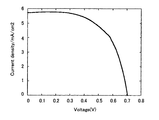
- 238000011156 evaluation Methods 0.000 description 1
- 238000010285 flame spraying Methods 0.000 description 1
- 239000011888 foil Substances 0.000 description 1
- 235000019253 formic acid Nutrition 0.000 description 1
- 239000000499 gel Substances 0.000 description 1
- RBTKNAXYKSUFRK-UHFFFAOYSA-N heliogen blue Chemical compound [Cu].[N-]1C2=C(C=CC=C3)C3=C1N=C([N-]1)C3=CC=CC=C3C1=NC([N-]1)=C(C=CC=C3)C3=C1N=C([N-]1)C3=CC=CC=C3C1=N2 RBTKNAXYKSUFRK-UHFFFAOYSA-N 0.000 description 1
- 230000005525 hole transport Effects 0.000 description 1
- 239000012943 hotmelt Substances 0.000 description 1
- 239000001257 hydrogen Substances 0.000 description 1
- 229910052739 hydrogen Inorganic materials 0.000 description 1
- AMGQUBHHOARCQH-UHFFFAOYSA-N indium;oxotin Chemical compound [In].[Sn]=O AMGQUBHHOARCQH-UHFFFAOYSA-N 0.000 description 1
- 238000009434 installation Methods 0.000 description 1
- 150000004694 iodide salts Chemical class 0.000 description 1
- PNDPGZBMCMUPRI-UHFFFAOYSA-N iodine Chemical compound II PNDPGZBMCMUPRI-UHFFFAOYSA-N 0.000 description 1
- 238000007733 ion plating Methods 0.000 description 1
- 150000002500 ions Chemical class 0.000 description 1
- 239000004310 lactic acid Substances 0.000 description 1
- 235000014655 lactic acid Nutrition 0.000 description 1
- 238000001182 laser chemical vapour deposition Methods 0.000 description 1
- 230000031700 light absorption Effects 0.000 description 1
- 239000007788 liquid Substances 0.000 description 1
- 229910052943 magnesium sulfate Inorganic materials 0.000 description 1
- 235000019341 magnesium sulphate Nutrition 0.000 description 1
- 150000002739 metals Chemical class 0.000 description 1
- 229910052750 molybdenum Inorganic materials 0.000 description 1
- 239000011733 molybdenum Substances 0.000 description 1
- 229910021421 monocrystalline silicon Inorganic materials 0.000 description 1
- 229910000403 monosodium phosphate Inorganic materials 0.000 description 1
- 235000019799 monosodium phosphate Nutrition 0.000 description 1
- 229910000484 niobium oxide Inorganic materials 0.000 description 1
- URLJKFSTXLNXLG-UHFFFAOYSA-N niobium(5+);oxygen(2-) Chemical compound [O-2].[O-2].[O-2].[O-2].[O-2].[Nb+5].[Nb+5] URLJKFSTXLNXLG-UHFFFAOYSA-N 0.000 description 1
- 229910017604 nitric acid Inorganic materials 0.000 description 1
- 150000004767 nitrides Chemical class 0.000 description 1
- 229910052757 nitrogen Inorganic materials 0.000 description 1
- QGLKJKCYBOYXKC-UHFFFAOYSA-N nonaoxidotritungsten Chemical compound O=[W]1(=O)O[W](=O)(=O)O[W](=O)(=O)O1 QGLKJKCYBOYXKC-UHFFFAOYSA-N 0.000 description 1
- 239000003921 oil Substances 0.000 description 1
- 238000001579 optical reflectometry Methods 0.000 description 1
- 235000006408 oxalic acid Nutrition 0.000 description 1
- 230000033116 oxidation-reduction process Effects 0.000 description 1
- 230000001443 photoexcitation Effects 0.000 description 1
- 238000005268 plasma chemical vapour deposition Methods 0.000 description 1
- 238000007750 plasma spraying Methods 0.000 description 1
- 239000004033 plastic Substances 0.000 description 1
- 229920003023 plastic Polymers 0.000 description 1
- 239000013308 plastic optical fiber Substances 0.000 description 1
- 229920003229 poly(methyl methacrylate) Polymers 0.000 description 1
- 229920001088 polycarbazole Polymers 0.000 description 1
- 239000004417 polycarbonate Substances 0.000 description 1
- 229910021420 polycrystalline silicon Inorganic materials 0.000 description 1
- 229920000647 polyepoxide Polymers 0.000 description 1
- 229920001225 polyester resin Polymers 0.000 description 1
- 239000004645 polyester resin Substances 0.000 description 1
- 229920001223 polyethylene glycol Polymers 0.000 description 1
- 239000009719 polyimide resin Substances 0.000 description 1
- 229920000642 polymer Polymers 0.000 description 1
- 239000004926 polymethyl methacrylate Substances 0.000 description 1
- 229920005672 polyolefin resin Polymers 0.000 description 1
- 229920002223 polystyrene Polymers 0.000 description 1
- GCHCGDFZHOEXMP-UHFFFAOYSA-L potassium adipate Chemical compound [K+].[K+].[O-]C(=O)CCCCC([O-])=O GCHCGDFZHOEXMP-UHFFFAOYSA-L 0.000 description 1
- 239000001608 potassium adipate Substances 0.000 description 1
- 235000011051 potassium adipate Nutrition 0.000 description 1
- 239000004323 potassium nitrate Substances 0.000 description 1
- 235000010333 potassium nitrate Nutrition 0.000 description 1
- OTYBMLCTZGSZBG-UHFFFAOYSA-L potassium sulfate Chemical compound [K+].[K+].[O-]S([O-])(=O)=O OTYBMLCTZGSZBG-UHFFFAOYSA-L 0.000 description 1
- 229910052939 potassium sulfate Inorganic materials 0.000 description 1
- 235000011151 potassium sulphates Nutrition 0.000 description 1
- 239000001044 red dye Substances 0.000 description 1
- 238000006479 redox reaction Methods 0.000 description 1
- 238000007650 screen-printing Methods 0.000 description 1
- 239000000565 sealant Substances 0.000 description 1
- 239000000377 silicon dioxide Substances 0.000 description 1
- 239000002210 silicon-based material Substances 0.000 description 1
- 229920002379 silicone rubber Polymers 0.000 description 1
- 239000003707 silyl modified polymer Substances 0.000 description 1
- 239000001632 sodium acetate Substances 0.000 description 1
- 235000017281 sodium acetate Nutrition 0.000 description 1
- 235000017557 sodium bicarbonate Nutrition 0.000 description 1
- 229910000030 sodium bicarbonate Inorganic materials 0.000 description 1
- AJPJDKMHJJGVTQ-UHFFFAOYSA-M sodium dihydrogen phosphate Chemical compound [Na+].OP(O)([O-])=O AJPJDKMHJJGVTQ-UHFFFAOYSA-M 0.000 description 1
- 235000009518 sodium iodide Nutrition 0.000 description 1
- 239000001540 sodium lactate Substances 0.000 description 1
- 235000011088 sodium lactate Nutrition 0.000 description 1
- 229940005581 sodium lactate Drugs 0.000 description 1
- 239000004317 sodium nitrate Substances 0.000 description 1
- 235000010344 sodium nitrate Nutrition 0.000 description 1
- 229910052938 sodium sulfate Inorganic materials 0.000 description 1
- 235000011152 sodium sulphate Nutrition 0.000 description 1
- 229910052715 tantalum Inorganic materials 0.000 description 1
- GUVRBAGPIYLISA-UHFFFAOYSA-N tantalum atom Chemical compound [Ta] GUVRBAGPIYLISA-UHFFFAOYSA-N 0.000 description 1
- 238000002230 thermal chemical vapour deposition Methods 0.000 description 1
- 238000007751 thermal spraying Methods 0.000 description 1
- 239000010409 thin film Substances 0.000 description 1
- XOLBLPGZBRYERU-UHFFFAOYSA-N tin dioxide Chemical compound O=[Sn]=O XOLBLPGZBRYERU-UHFFFAOYSA-N 0.000 description 1
- 229910001887 tin oxide Inorganic materials 0.000 description 1
- 230000007704 transition Effects 0.000 description 1
- YNJBWRMUSHSURL-UHFFFAOYSA-N trichloroacetic acid Chemical compound OC(=O)C(Cl)(Cl)Cl YNJBWRMUSHSURL-UHFFFAOYSA-N 0.000 description 1
- ODHXBMXNKOYIBV-UHFFFAOYSA-N triphenylamine Chemical compound C1=CC=CC=C1N(C=1C=CC=CC=1)C1=CC=CC=C1 ODHXBMXNKOYIBV-UHFFFAOYSA-N 0.000 description 1
- 229910001930 tungsten oxide Inorganic materials 0.000 description 1
- 229910052720 vanadium Inorganic materials 0.000 description 1
- LEONUFNNVUYDNQ-UHFFFAOYSA-N vanadium atom Chemical compound [V] LEONUFNNVUYDNQ-UHFFFAOYSA-N 0.000 description 1
- 239000011787 zinc oxide Substances 0.000 description 1
Images


Classifications
-
- H—ELECTRICITY
- H01—ELECTRIC ELEMENTS
- H01G—CAPACITORS; CAPACITORS, RECTIFIERS, DETECTORS, SWITCHING DEVICES, LIGHT-SENSITIVE OR TEMPERATURE-SENSITIVE DEVICES OF THE ELECTROLYTIC TYPE
- H01G9/00—Electrolytic capacitors, rectifiers, detectors, switching devices, light-sensitive or temperature-sensitive devices; Processes of their manufacture
- H01G9/20—Light-sensitive devices
- H01G9/2027—Light-sensitive devices comprising an oxide semiconductor electrode
- H01G9/2031—Light-sensitive devices comprising an oxide semiconductor electrode comprising titanium oxide, e.g. TiO2
-
- H—ELECTRICITY
- H01—ELECTRIC ELEMENTS
- H01G—CAPACITORS; CAPACITORS, RECTIFIERS, DETECTORS, SWITCHING DEVICES, LIGHT-SENSITIVE OR TEMPERATURE-SENSITIVE DEVICES OF THE ELECTROLYTIC TYPE
- H01G9/00—Electrolytic capacitors, rectifiers, detectors, switching devices, light-sensitive or temperature-sensitive devices; Processes of their manufacture
- H01G9/0029—Processes of manufacture
-
- H—ELECTRICITY
- H01—ELECTRIC ELEMENTS
- H01G—CAPACITORS; CAPACITORS, RECTIFIERS, DETECTORS, SWITCHING DEVICES, LIGHT-SENSITIVE OR TEMPERATURE-SENSITIVE DEVICES OF THE ELECTROLYTIC TYPE
- H01G9/00—Electrolytic capacitors, rectifiers, detectors, switching devices, light-sensitive or temperature-sensitive devices; Processes of their manufacture
- H01G9/20—Light-sensitive devices
- H01G9/2022—Light-sensitive devices characterized by he counter electrode
-
- H—ELECTRICITY
- H01—ELECTRIC ELEMENTS
- H01G—CAPACITORS; CAPACITORS, RECTIFIERS, DETECTORS, SWITCHING DEVICES, LIGHT-SENSITIVE OR TEMPERATURE-SENSITIVE DEVICES OF THE ELECTROLYTIC TYPE
- H01G9/00—Electrolytic capacitors, rectifiers, detectors, switching devices, light-sensitive or temperature-sensitive devices; Processes of their manufacture
- H01G9/20—Light-sensitive devices
- H01G9/209—Light trapping arrangements
-
- Y—GENERAL TAGGING OF NEW TECHNOLOGICAL DEVELOPMENTS; GENERAL TAGGING OF CROSS-SECTIONAL TECHNOLOGIES SPANNING OVER SEVERAL SECTIONS OF THE IPC; TECHNICAL SUBJECTS COVERED BY FORMER USPC CROSS-REFERENCE ART COLLECTIONS [XRACs] AND DIGESTS
- Y02—TECHNOLOGIES OR APPLICATIONS FOR MITIGATION OR ADAPTATION AGAINST CLIMATE CHANGE
- Y02E—REDUCTION OF GREENHOUSE GAS [GHG] EMISSIONS, RELATED TO ENERGY GENERATION, TRANSMISSION OR DISTRIBUTION
- Y02E10/00—Energy generation through renewable energy sources
- Y02E10/50—Photovoltaic [PV] energy
- Y02E10/542—Dye sensitized solar cells
-
- Y—GENERAL TAGGING OF NEW TECHNOLOGICAL DEVELOPMENTS; GENERAL TAGGING OF CROSS-SECTIONAL TECHNOLOGIES SPANNING OVER SEVERAL SECTIONS OF THE IPC; TECHNICAL SUBJECTS COVERED BY FORMER USPC CROSS-REFERENCE ART COLLECTIONS [XRACs] AND DIGESTS
- Y02—TECHNOLOGIES OR APPLICATIONS FOR MITIGATION OR ADAPTATION AGAINST CLIMATE CHANGE
- Y02P—CLIMATE CHANGE MITIGATION TECHNOLOGIES IN THE PRODUCTION OR PROCESSING OF GOODS
- Y02P70/00—Climate change mitigation technologies in the production process for final industrial or consumer products
- Y02P70/50—Manufacturing or production processes characterised by the final manufactured product
Definitions
- the present invention relates to a dye-sensitized solar cell.
- solar cells such as single crystal, polycrystalline or amorphous silicon solar cells, compound semiconductor solar cells such as CIGS, CdTe, and GaAs, organic thin film solar cells, and dye-sensitized solar cells.
- silicon solar cells are the mainstream.
- a silicon-type solar cell requires a high-purity silicon material.
- silicon type solar cells need to be manufactured under high temperature and high vacuum, and there is room for improvement in terms of high manufacturing cost.
- dye-sensitized solar cells have attracted attention.
- the dye-sensitized solar cell can be easily manufactured because of its simple structure, and the constituent materials are abundant.
- the dye-sensitized solar cell can be manufactured at low cost and has high photoelectric conversion efficiency. Therefore, the dye-sensitized solar cell has attracted attention as a next-generation solar cell.
- the dye-sensitized solar cell has a simple method of sealing and connecting the photoelectrode and the counter electrode after injecting an electrolytic solution having reversible electrochemical redox characteristics between the photoelectrode and the counter electrode. Can be built.
- the photoelectrode is conventionally produced by the following method. First, a paste containing titanium oxide fine particles is coated on the surface of a glass substrate on which a transparent conductive film such as ITO (Indium Tin Oxide) or FTO (Fluorine Tin Oxide) is formed. Next, the obtained coating is heat-treated at a temperature of 400 to 500 ° C. to produce an electrode having a porous titanium oxide layer. Next, a photoelectrode in which the dye sensitizer is adsorbed on the surface of the porous titanium oxide by immersing the obtained electrode in an organic solution containing a dye sensitizer such as a ruthenium dye or an indoline dye Is made.
- a dye sensitizer such as a ruthenium dye or an indoline dye Is made.
- the counter electrode is produced by forming a catalyst layer (for example, a platinum layer) that exhibits an electrochemical reduction action on a glass substrate on which a transparent conductive film is formed by a technique such as sputtering.
- a catalyst layer for example, a platinum layer
- the transparent conductive film constituting the photoelectrode and the counter electrode has a relatively large electric resistance. Therefore, there is room for improvement in that the photoelectric conversion efficiency of the obtained dye-sensitized solar cell is significantly reduced when the coating area of titanium oxide (area of the transparent conductive film) is increased. Moreover, the electrical resistance of a transparent conductive film becomes large by the heat processing at the time of producing a porous titanium oxide layer (titanium oxide sintered body). Therefore, there is room for improvement in that the photoelectric conversion efficiency of the dye-sensitized solar cell is reduced.
- This technique has a lower electrical resistance value than a conventional glass substrate on which a transparent conductive film is formed, and has corrosion resistance against iodine and the like contained in an electrolyte solution used in a dye-sensitized solar cell.
- Patent Document 1 discloses a semiconductor film that is a porous titania film that has adsorbed a dye sensitizer, an electrode that supports the semiconductor film, a counter electrode that is placed facing the electrode, and an electrode and a counter electrode.
- a dye-sensitized solar cell is disclosed that includes an electrolyte layer responsible for charge transport between the two.
- a metal substrate is used as an electrode carrying a porous titania film adsorbed with a dye sensitizer, a conductive film having an opening is used as a counter electrode, and the counter electrode side is a light receiving surface. It is.
- the metal substrate is made of titanium or the like, and the conductive film is platinum or the like.
- the opening has a mesh shape or a stripe shape.
- this dye-sensitized solar cell requires light irradiation from the counter electrode side, and light reaches the dye adsorbed on the porous titania film of the electrode through the colored electrolyte solution. Therefore, there is room for improvement in that the light is attenuated and the photoelectric conversion efficiency of the obtained dye-sensitized solar cell is lowered.
- the present inventor has developed a new dye-sensitized solar cell (Patent Document 2).
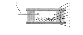
- the photoelectrode and the counter electrode are arranged to face each other with an electrolyte layer interposed therebetween.
- the photoelectrode is dye-sensitized on a titanium material having an opening.
- a semiconductor layer containing an agent is formed,
- a light collecting device is disposed on the titanium material of the photoelectrode, and (3) a fiber member or a glass rod on the titanium material having an opening. The material is embedded.
- JP 2010-55935 A Patent No. 5161967
- An object of the present invention is to provide a dye-sensitized solar cell having high photoelectric conversion efficiency and good durability.
- the present inventor has intensively studied to solve the problems of the prior art and found that a dye-sensitized solar cell having a specific structure can achieve the above object.
- the present invention is the following dye-sensitized solar cell.
- a dye-sensitized solar cell in which a photoelectrode and a counter electrode are arranged to face each other via an electrolyte layer, (1) The photoelectrode is formed by forming a semiconductor layer containing a dye sensitizer on a metal titanium material or a titanium alloy material, (2) The counter electrode is a metal titanium material or titanium alloy material coated with an electrochemical reduction catalyst layer, (3) A light irradiation means is disposed between the photoelectrode and the counter electrode.
- a dye-sensitized solar cell characterized by the above.
- Item 2. The dye-sensitized solar cell according to Item 1, wherein the semiconductor layer is composed of titanium oxide.
- Item 3 The dye-sensitized solar cell according to Item 1 or 2, wherein the electrochemical reduction catalyst layer is a platinum catalyst layer.
- Item 4. The light emitting device according to any one of Items 1 to 3, wherein the light irradiating unit collects sunlight or room light with a condensing device and transmits the collected light to a dye-sensitized solar cell using an optical fiber. The dye-sensitized solar cell described.
- the light irradiating means collects sunlight or room light with a condensing device, and transmits the collected light to a dye-sensitized solar cell using an optical fiber, Item 5.
- the dye-sensitized solar cell according to any one of Items 1 to 4, wherein a member that emits the transmitted light is disposed in the dye-sensitized solar cell.
- Item 6 The dye-sensitized solar cell according to any one of Items 1 to 3, wherein the light irradiation means uses an LED or an organic EL.
- Item 7. The dye-sensitized solar cell according to any one of Items 1 to 6, wherein the photoelectrode comprises a photoelectrode substrate having a semiconductor layer having anatase-type titanium oxide on its surface, which is produced by the following method. : (1) a step of forming titanium nitride on the surface of the metal titanium material or titanium alloy material, and (2) a metal titanium material or titanium alloy material obtained in step (1) and having titanium nitride formed on the surface. A process of forming an anatase-type titanium oxide film by anodizing at a voltage higher than the spark discharge voltage using an electrolytic solution having an etching action on titanium.
- Item 8 The dye-sensitized solar cell according to any one of Items 1 to 6, wherein the photoelectrode comprises a photoelectrode substrate having a semiconductor layer having anatase-type titanium oxide on its surface, which is produced by the following method. : (1) a step of forming titanium nitride on the surface of the titanium metal material or titanium alloy material; (2) A step of anodizing the metal titanium material or titanium alloy material having titanium nitride formed on the surface obtained in step (1) in an electrolyte solution having no etching action on titanium, And (3) A step of heat-treating the anodized metal titanium material or titanium alloy material obtained in step (2) in an oxidizing atmosphere to form an anatase-type titanium oxide film.
- Item 9 The step of forming the titanium nitride is performed by one kind of treatment method selected from the group consisting of PVD treatment, CVD treatment, thermal spray treatment, heat treatment under an ammonia gas atmosphere, and heat treatment under a nitrogen gas atmosphere.
- Item 9 The dye-sensitized solar cell according to Item 7 or 8, wherein
- Item 10 The manufacturing method according to Item 9, wherein the heat treatment under the nitrogen gas atmosphere is performed in the presence of an oxygen trap agent.
- the dye-sensitized solar cell of the present invention has high photoelectric conversion efficiency and good durability.
- the metal titanium material and the titanium alloy material may be simply referred to as a titanium material.
- the dye-sensitized solar cell of the present invention is The photoelectrode and the counter electrode are arranged opposite to each other with the electrolyte layer interposed therebetween, (1)
- the photoelectrode is formed by forming a semiconductor layer containing a dye sensitizer on a metal titanium material or a titanium alloy material, (2)
- the counter electrode is a metal titanium material or titanium alloy material coated with an electrochemical reduction catalyst layer, (3)
- a light irradiation means is disposed between the photoelectrode and the counter electrode. It is characterized by that.
- the dye-sensitized solar cell of the present invention is composed of a photoelectrode and a counter electrode made of a titanium material that does not transmit light. Light irradiation by the light irradiation means is performed between the photoelectrode and the counter electrode. As a result, the dye-sensitized solar cell of the present invention can exhibit high photoelectric conversion efficiency based on the light confinement effect.
- the dye-sensitized solar cell of the present invention can employ a light irradiation method by removing light such as ultraviolet rays that causes deterioration of the dye sensitizer by the light irradiation means. Furthermore, the sealing means of a dye-sensitized solar cell can be performed at low cost. As a result, the dye-sensitized solar cell of the present invention has good durability.
- the dye-sensitized solar cell of the present invention does not require sealing the opening of a titanium material having a conventional opening with a fiber member or a glass rod material.
- the dye-sensitized solar cell of the present invention can prevent leakage of the highly volatile electrolyte and has good durability.
- a photoelectrode and a counter electrode are arranged to face each other with an electrolyte layer interposed therebetween.
- the photoelectrode is obtained by forming a semiconductor layer containing a dye sensitizer on a metal titanium material or a titanium alloy material (hereinafter, also referred to as “titanium material”).
- Titanium material becomes a base material.
- Metallic titanium material is titanium itself.
- the type is not particularly limited.
- the titanium alloy include Ti-6Al-4V, Ti-4.5Al-3V-2Fe-2Mo, Ti-0.5Pd, and the like.
- the photoelectrode substrate is the following for the titanium material, for the purpose of preventing leakage of electrons to the electrolyte layer when electrons accompanying photoexcitation of the dye sensitizer migrate from the semiconductor layer to the photoelectrode substrate. It is preferable to use a surface treatment method A or B which is formed by forming an anatase-type titanium oxide film on the surface of the titanium material. The film of anatase type titanium oxide becomes a semiconductor layer.
- the dye-sensitized solar cell of the present invention has a high photoelectric conversion efficiency because the photoelectrode substrate has a semiconductor layer containing a dye sensitizer formed on a titanium material.
- the thickness of the photoelectrode substrate is usually about 0.01 to 10 mm, preferably about 0.01 to 5 mm, more preferably about 0.05 to 1 mm.
- the photoelectrode substrate is preferably composed of a photoelectrode substrate having a semiconductor layer having anatase-type titanium oxide on the surface, which is produced by the following method. (1) a step of forming titanium nitride on the surface of the metal titanium material or titanium alloy material, and (2) a metal titanium material or titanium alloy material obtained in step (1) and having titanium nitride formed on the surface. A process of forming an anatase-type titanium oxide film by anodizing at a voltage higher than the spark discharge voltage using an electrolytic solution having an etching action on titanium.
- the photoelectrode substrate is preferably composed of a photoelectrode substrate having a semiconductor layer having anatase-type titanium oxide on the surface, which is produced by the following method. (1) a step of forming titanium nitride on the surface of the titanium metal material or titanium alloy material; (2) A step of anodizing the metal titanium material or titanium alloy material having titanium nitride formed on the surface obtained in step (1) in an electrolyte solution having no etching action on titanium, And (3) A step of heat-treating the anodized metal titanium material or titanium alloy material obtained in step (2) in an oxidizing atmosphere to form an anatase-type titanium oxide film.
- Step (1) of surface treatment methods A and B In the step of forming titanium nitride on the surface of the titanium material (step (1)), a layer of titanium nitride can be formed on the surface of the titanium material, usually about 0.1 to 100 ⁇ m.
- the titanium nitride layer is preferably about 0.5 to 50 ⁇ m, more preferably about 1 to 10 ⁇ m.
- the means for forming titanium nitride on the surface of the titanium material is not particularly limited.
- the titanium nitride formation process includes PVD treatment (physical vapor deposition), CVD treatment (chemical vapor deposition), thermal spray treatment (film formation by spraying), heat treatment in an ammonia gas atmosphere, and nitrogen gas atmosphere. It is preferable to carry out by one kind of treatment method selected from the group consisting of the heat treatment in [1].
- PVD treatment includes ion plating and sputtering.
- CVD process include a thermal CVD process, a plasma CVD process, and a laser CVD process.
- thermal spraying process include flame spraying, arc spraying, plasma spraying, and laser spraying.
- the heating temperature of the heat treatment in an ammonia gas or nitrogen gas atmosphere is preferably about 500 ° C. or higher, more preferably about 750 to 1050 ° C., and further preferably about 750 ° C. to 950 ° C.
- a method of heating the titanium material at about 500 ° C. or higher (preferably about 750 ° C. or higher) in a nitrogen gas atmosphere is preferable.
- the heat treatment in an ammonia gas or nitrogen gas atmosphere is preferably performed in the presence of an oxygen trap agent.
- titanium nitride by performing a heat treatment in a nitrogen gas atmosphere in the presence of an oxygen trap agent.
- oxygen trap agent used in the heat treatment of the titanium material examples include a substance or gas having a higher affinity for oxygen than the titanium material.
- carbon materials, metal powder, hydrogen gas, etc. are preferable materials.
- These oxygen trap agents may be used individually by 1 type, and may be used in combination of 2 or more type.
- the carbon material is not particularly limited, and examples thereof include graphitic carbon, amorphous carbon, and carbon having an intermediate crystal structure.
- the carbon material may have any shape such as a flat plate shape, a foil shape, and a powder shape. It is preferable to use a flat carbon material because it is easy to handle and prevents thermal distortion during the heat treatment of the titanium material.
- the metal powder is not particularly limited.
- metal powder such as titanium, titanium alloy, chromium, chromium alloy, zirconium, zirconium alloy, aluminum, aluminum alloy.
- the most preferable metal powder is fine particle titanium or titanium alloy metal powder.
- the said metal powder may be used individually by 1 type, and may be used in combination of 2 or more type.
- the average particle diameter of the metal powder is preferably about 0.1 to 1000 ⁇ m, more preferably about 0.1 to 100 ⁇ m, and still more preferably about 0.1 to 10 ⁇ m.
- the conditions for using the oxygen trap agent in an ammonia gas or nitrogen gas atmosphere can be set in a timely manner according to the type and shape of the oxygen trap agent.
- a carbon material or metal powder is used as an oxygen trap agent
- the carbon material or metal powder is brought into contact with the titanium material, the surface of the titanium material is covered with the carbon material or metal powder, and the titanium material is covered with ammonia gas or
- the method of heat-processing in nitrogen gas atmosphere is mentioned.
- hydrogen gas is used as the oxygen trap agent, there is a method in which the titanium material is heat-treated in a state where hydrogen gas is introduced in an atmosphere of ammonia gas or nitrogen gas.
- Heat treatment can be performed in an atmosphere of ammonia gas, nitrogen gas, or a mixed gas of ammonia gas and nitrogen gas. Considering simplicity, economy and safety, it is most preferable to use nitrogen gas.
- the reaction pressure of the heat treatment in an ammonia gas or nitrogen gas atmosphere is about 0.01 to 100 MPa, preferably about 0.1 to 10 MPa, more preferably about 0.1 to 1 MPa. Heat treatment in a nitrogen gas atmosphere is preferable.
- the heating time of the heat treatment under an ammonia gas or nitrogen gas atmosphere is preferably about 1 minute to 12 hours, more preferably about 10 minutes to 8 hours, and further preferably about 1 hour to 6 hours. It is preferable to heat-treat the titanium material for this time.
- titanium nitride In the method of heat-treating titanium material in an atmosphere of ammonia gas or nitrogen gas, in order to efficiently form titanium nitride on the surface of the titanium material, a rotary vacuum pump, mechanical booster pump, or oil diffusion pump is used as necessary. It is preferable that the inside of the furnace to be heat-treated is depressurized to reduce the oxygen concentration remaining in the furnace to be heat-treated (inside the nitriding furnace). Titanium nitride can be efficiently formed on the surface of the titanium material by reducing the pressure in the furnace for the heat treatment to about 10 Pa or less, more preferably about 1 Pa or less, and even more preferably about 0.1 Pa or less.
- the inside of the furnace is decompressed, and the titanium material is heat-treated, so that the surface of the titanium material is heated. Titanium nitride can be formed efficiently.
- the heating temperature, heating time, etc. of the heat treatment using the main furnace the same conditions as described above may be used.
- the gas composition it is most preferable to use nitrogen gas in consideration of simplicity, economy, and safety.
- the surface of the titanium material is made of titanium.
- Nitride can be formed more efficiently.
- titanium nitride can be more efficiently formed on the surface of the titanium material by performing pressure reduction treatment in the presence of an oxygen trap agent and heat treatment in a gas atmosphere such as ammonia gas or nitrogen gas.
- the type of titanium nitride formed on the surface of the titanium material is not particularly limited.
- TiN, Ti 2 N, and a mixture thereof, more preferably TiN, and a mixture of TiN and Ti 2 N, particularly preferably TiN are exemplified.
- one of the above methods may be performed alone, or two or more methods may be arbitrarily combined.
- heat treatment of the titanium material in a nitrogen gas atmosphere is preferable.
- Step (2) of surface treatment method A an anatase-type titanium oxide is obtained by anodizing a titanium material having titanium nitride formed on the surface thereof using an electrolytic solution having an etching action on titanium at a spark discharge generation voltage or higher. Is formed (step (2)).
- a photoelectrode substrate having a semiconductor layer having anatase-type titanium oxide on the surface can be produced.
- an anatase-type titanium oxide film can be suitably formed.
- high photoelectric conversion efficiency can be suitably exhibited.
- an electrolytic solution having an etching action on the titanium material is preferable.
- the electrolytic solution preferably contains an inorganic acid and / or an organic acid having an etching action on titanium. It is preferable that the electrolytic solution further contains hydrogen peroxide.
- Anodization is preferably performed by applying a voltage equal to or higher than the discharge generation voltage.
- an aqueous solution containing an inorganic acid having an etching action on the titanium material and / or an organic acid having the action examples include sulfuric acid, hydrofluoric acid, hydrochloric acid, nitric acid, and aqua regia.
- action with respect to titanium an oxalic acid, a formic acid, a citric acid, a trichloroacetic acid etc. are mentioned, for example. These acids may be used alone or in combination of two or more of these acids regardless of whether they are organic acids or inorganic acids.
- An example of a preferable embodiment of the electrolytic solution containing two or more acids includes an aqueous solution containing phosphoric acid as required in sulfuric acid.
- the mixing ratio of the acid in the electrolytic solution varies depending on the type of acid used, anodizing conditions, and the like, but is usually 0.01 to 10M, preferably 0.1 to 10M, more preferably 1 to 10M in terms of the total amount of the acid. Can be mentioned.
- an electrolytic solution containing sulfuric acid and phosphoric acid an electrolytic solution containing sulfuric acid 1 to 8M and phosphoric acid 0.1 to 2M can be exemplified.
- the electrolyte solution preferably contains hydrogen peroxide in addition to the organic acid and / or inorganic acid.
- hydrogen peroxide in addition to the organic acid and / or inorganic acid.
- the electrolytic solution By containing hydrogen peroxide in the electrolytic solution, it becomes possible to prepare a film of anatase-type titanium oxide more efficiently.
- the blending ratio is not particularly limited, but for example, a ratio of 0.01 to 5M, preferably 0.01 to 1M, and more preferably 0.1 to 1M is exemplified.
- an aqueous solution containing sulfuric acid 1 to 8M, phosphoric acid 0.1 to 2M and hydrogen peroxide 0.1 to 1M can be cited.
- An anatase-type titanium oxide film can be obtained by immersing a titanium material in the electrolyte and applying a constant current so that a voltage equal to or higher than the spark discharge voltage can be applied.
- the voltage higher than the spark discharge generation voltage is typically 100 V or higher, preferably 150 V or higher.
- Anodization can be performed, for example, by increasing the voltage at a constant rate up to the spark discharge generation voltage and applying a constant voltage for a certain time at a voltage equal to or higher than the spark discharge generation voltage.
- the speed at which the voltage is increased to the spark discharge generation voltage is usually set to 0.01 to 1 V / second, preferably 0.05 to 0.5 V / second, more preferably 0.1 to 0.5 V / second.
- the time for applying a voltage higher than the spark discharge generation voltage is usually set to 1 minute or longer, preferably 1 to 60 minutes, and more preferably 10 to 30 minutes.
- Anodization by spark discharge can be performed by controlling the current instead of controlling the voltage.
- the current density may be 0.1 A / dm 2 or more, but 1 A / dm 2 to 10 A / dm 2 is preferable from the viewpoint of economy, simplicity, and performance.
- a film containing anatase-type titanium oxide having a film thickness of about 1 to 100 ⁇ m can be obtained.
- Step (2) of surface treatment method B In the surface treatment method B, a titanium material having titanium nitride formed on the surface is anodized in an electrolyte solution that does not have an etching action on titanium (step (2)), and then anodized. The obtained titanium material is heat-treated in an oxidizing atmosphere to form an anatase-type titanium oxide film (step (3)). A photoelectrode substrate having a semiconductor layer having anatase-type titanium oxide on the surface can be produced.
- the electrolytic solution preferably contains at least one acid selected from the group consisting of inorganic acids and organic acids that do not have an etching action on titanium and a salt compound thereof.
- Amorphous titanium oxide film is formed on the surface of the titanium material by anodizing the titanium material with titanium nitride formed on the surface in an electrolyte that does not etch titanium. can do.
- an electrolytic solution containing at least one compound selected from the group consisting of inorganic acids, organic acids and salts thereof (hereinafter also referred to as “inorganic acids etc.”) It is preferable that The electrolytic solution containing the inorganic acid or the like is preferably a dilute aqueous solution such as phosphoric acid or phosphate.
- step (2) of performing the anodic oxidation in the surface treatment method B is a condition in which spark discharge does not occur, and usually, crystalline titanium oxide such as anatase-type titanium oxide is not formed.
- anatase-type titanium oxide can be formed from amorphous titanium oxide. Therefore, for the reason that an amorphous titanium oxide film is effectively formed on the surface of the titanium material, it is preferable to anodize the titanium material having titanium nitride formed on the surface.
- At least one compound (inorganic acid, etc.) selected from the group consisting of inorganic acids (phosphoric acid, etc.), organic acids and salts thereof (phosphates, etc.) ) Is preferable.
- inorganic acid that does not have an etching action on titanium phosphoric acid, carbonic acid, and the like are preferable in consideration of convenience, economy, safety, and the like.
- organic acid having no etching action on titanium acetic acid, adipic acid, lactic acid and the like are preferable.
- salts of these acids such as sodium dihydrogen phosphate, disodium hydrogen phosphate, sodium hydrogen carbonate, sodium acetate, potassium adipate, sodium lactate and the like can also be used.
- an electrolytic solution containing an electrolyte such as sodium sulfate, potassium sulfate, magnesium sulfate, sodium nitrate, potassium nitrate, magnesium nitrate, calcium nitrate.
- At least one compound (inorganic acid, etc.) selected from the group consisting of inorganic acids (phosphoric acid, etc.), organic acids and salts thereof (phosphates, etc.) ) Is preferable.
- inorganic acid phosphoric acid and phosphate are most preferable.
- the electrolytic solution is preferably a dilute aqueous solution such as an inorganic acid.
- concentration of the inorganic acid or the like in the electrolytic solution is preferably in the range of about 1% by weight for reasons such as economy.
- a concentration range of about 0.01 to 10% by weight is preferable, a concentration range of about 0.1 to 10% by weight is more preferable, and a concentration range of about 1 to 3% by weight is more preferable.
- these acids may be used alone or in combination of two or more of these acids regardless of whether they are organic acids or inorganic acids.
- the aqueous solution containing a phosphate and phosphoric acid is mentioned.
- the mixing ratio of the acid in the electrolytic solution varies depending on the type of acid and acid salt used, anodizing conditions, and the like, but is generally 0.01 to 10% by weight, preferably 0.1 to 10% by weight, based on the total amount of the acid. More preferably, the ratio is 1 to 3% by weight.
- a titanium material in which titanium nitride is formed on the surface obtained in the step of forming titanium nitride is immersed in a dilute electrolytic solution containing an inorganic acid or the like that has no etching action on titanium.
- anodic oxidation is preferably performed by applying a voltage of about 10 to 300V. It is more preferable to perform anodization at a voltage of about 50 to 300V, and it is further preferable to perform anodization at a voltage of about 50 to 200V.
- the treatment temperature for anodization is preferably about 0 to 80 ° C. for reasons such as simplicity, economy and safety. It is more preferable to perform anodization at a temperature of about 10 to 50 ° C, and it is more preferable to perform anodization at a temperature of about 20 to 30 ° C.
- the treatment time for anodization is preferably about 1 second to 1 hour. It is more preferable to perform anodization in a time of about 10 seconds to 30 minutes, and it is further preferable to perform anodization in a time of about 5 minutes to 20 minutes.
- Step (3) of surface treatment method B the titanium material having a titanium oxide film formed on the surface is subjected to heat treatment in an oxidizing atmosphere to form an anatase-type titanium oxide film (step (3)).
- metal titanium material or the like is simply heat-treated in an oxidizing atmosphere, rutile titanium oxide is formed, but anatase titanium oxide is not sufficiently formed.
- Titanium material titanium material after anodization on which titanium nitride is formed and an oxide film of titanium (amorphous titanium oxide film) is heated in an oxidizing atmosphere (atmospheric oxidation, etc.)
- an oxidizing atmosphere atmospheric oxidation, etc.
- the oxidizing atmosphere for performing the heat treatment may be selected from an air oxidizing atmosphere, an atmosphere having an arbitrary oxygen gas concentration in which oxygen gas and nitrogen gas are mixed, an oxygen gas atmosphere, etc., but is simple and economical. For reasons such as safety, heat treatment in an atmospheric oxidizing atmosphere is preferable.
- the temperature of the heat treatment is preferably about 300 ° C. or higher because it efficiently changes from amorphous titanium oxide to anatase-type titanium oxide.
- the temperature of the heat treatment in an oxidizing atmosphere is preferably about 800 ° C. or less because it prevents phase transition from anatase-type titanium oxide to rutile-type titanium oxide. This is because rutile type titanium oxide has poor photoelectric conversion characteristics compared to anatase type titanium oxide.
- the temperature of the heat treatment in the oxidizing atmosphere is more preferably about 300 to 800 ° C, further preferably about 300 to 700 ° C, and particularly preferably about 400 to 700 ° C.
- the reaction pressure for performing the heat treatment is about 0.01 to 10 MPa, preferably about 0.01 to 5 MPa, and more preferably about 0.1 to 1 MPa.
- the heating time for performing the heat treatment is preferably about 1 minute to 12 hours, more preferably about 10 minutes to 8 hours, and further preferably about 1 hour to 6 hours.
- the crystalline titanium oxide film is preferably an anatase type titanium oxide film.
- Anatase-type titanium oxide has high photoelectric conversion characteristics because the open-circuit voltage value is improved compared to the use of rutile-type titanium oxide for the photoelectrode of a dye-sensitized solar cell.
- a film having a large amount of anatase-type titanium oxide having a high photocatalytic activity can be formed.
- a material for a photoelectric conversion element in which a large amount of highly active anatase-type titanium oxide is formed on the surface of the titanium material can be prepared by heat treatment. It is also possible to use it for a photoelectric conversion element material that achieves high conversion efficiency.
- a film containing anatase-type titanium oxide having a film thickness of about 1 to 100 ⁇ m can be obtained.
- a dilute acidic aqueous solution that does not have etching properties with respect to titanium such as phosphoric acid, phosphoric acid, after titanium nitride is formed on the surface of the titanium material, and after the titanium nitride is formed and before heat treatment in an oxidizing atmosphere By incorporating a step of anodizing in an electrolytic solution such as an aqueous solution of a salt such as, an excellent material for a photoelectric conversion element can be produced.
- Titanium materials are used as materials for photoelectric conversion elements such as photoelectrode substrates of dye-sensitized solar cells that are attracting attention as next-generation solar cells because anatase-type titanium oxide (film) is formed on the surface of these materials. be able to.
- the semiconductor layer photoelectrode is obtained by forming a semiconductor layer containing a dye sensitizer on a titanium material.
- the anatase-type titanium oxide film prepared by the surface treatment methods A and B may form a semiconductor layer. Furthermore, a semiconductor layer can be formed by applying a paste containing fine particles such as titanium oxide and then performing a heat treatment in an oxidizing atmosphere.
- the semiconductor layer is preferably composed of a metal oxide such as titanium oxide, zinc oxide, tin oxide, niobium oxide, or tungsten oxide.
- metal oxides may be used alone or in combination of two or more.
- titanium oxide is preferable.
- the semiconductor layer has a large difference between the flat band potential of the semiconductor that determines the open-circuit voltage of the photoelectrode and the oxidation-reduction potential of the electrolyte, and the electron injection from the dye sensitizer to the semiconductor is efficient. For reasons such as progress, those composed of titanium oxide are preferred.
- the average particle diameter of the titanium oxide fine particles is preferably about 0.1 to 3000 nm, more preferably about 1 to 1000 nm, and further preferably about 10 to 500 nm.
- the paste agent can be prepared, for example, by dispersing titanium oxide fine particles in a solvent.
- a solvent polyethylene glycol is preferable.
- the content of the titanium oxide fine particles in the paste is not particularly limited, and may be appropriately adjusted so that the sintered body is suitably formed.
- the method for applying the paste onto the titanium material is not particularly limited, and examples thereof include screen printing, inkjet, roll coating, doctor blade, spray coating, and the like.
- the thickness of the coating film after applying the paste agent is not particularly limited, and may be set as appropriate so that a titanium oxide sintered body having a target thickness is formed.
- the semiconductor layer As the semiconductor layer, a laminate of the titanium oxide sintered body and the titanium oxide film is obtained.
- the temperature of the heat treatment is preferably about 100 to 600 ° C, more preferably about 400 to 500 ° C.
- the titanium oxide fine particles can be suitably sintered by heat treatment at a temperature of about 400 to 500 ° C. What is necessary is just to set the time of heat processing suitably according to heat processing temperature.
- the heat treatment is performed in an oxidizing atmosphere (for example, in an atmosphere in which oxygen exists such as air).
- the dye sensitizer photoelectrode is obtained by forming a semiconductor layer containing a dye sensitizer on a titanium material.
- the dye sensitizer can be adsorbed on the titanium oxide (semiconductor layer) by immersing the photoelectrode on which the semiconductor layer is formed by the above-described method in a solution containing the dye sensitizer.
- the dye sensitizer is not particularly limited as long as it is a dye having light absorption in the near infrared light region and the visible light region.
- ruthenium metal complexes such as red dye (N719) and black dye (N749); metal complexes other than ruthenium such as copper phthalocyanine; These dye sensitizers can be used alone or in combination of two or more.
- a ruthenium complex is most preferable.
- adsorbing the dye sensitizer to the titanium oxide layer there is a method of immersing a semiconductor layer such as a titanium oxide layer in a solution containing the dye sensitizer.
- the dye sensitizer can be attached (chemical adsorption, physical adsorption, deposition, etc.) to the semiconductor layer.
- the amount of the dye sensitizer to be attached may be appropriately set according to the area of the semiconductor layer and the like within a range that does not impair the effects of the present invention.
- the counter electrode is obtained by coating an electrochemical reduction catalyst layer on a titanium metal material or a titanium alloy material (titanium material).
- the electrochemical reduction catalyst layer platinum catalyst layer, carbon layer, poly (3,4-ethylenedioxythiophene) (PEDOT) layer, gold layer, silver layer, copper layer, aluminum layer, rhodium layer, indium layer, etc. Can be used.
- the electrochemical reduction catalyst layer is preferably a platinum catalyst layer because, for example, electrons are easily injected into the electrolyte that has lost electrons in the electrolytic layer because the hydrogen overvoltage is low.
- the titanium material described above can be used as the titanium material.
- a liquid electrolyte layer is employed as the electrolyte layer, titanium as a counter electrode has no fear of corrosion due to iodine or the like which is a highly corrosive halogen group compound contained in the electrolyte layer.
- the thickness of the platinum catalyst layer is preferably about 0.001 to 2 ⁇ m.
- titanium or titanium alloy that has been subjected to a mirror finish so that light is easily reflected is preferable.
- a method selected from electrolytic plating, PVD treatment, CVD treatment, etc. may be adopted.
- the material constituting the counter electrode may further include metals such as platinum, gold, silver, copper, aluminum, rhodium and indium; carbon; conductive metal oxides such as ITO and FTO.
- the metal, metal oxide, etc. are used as a support, and a film having a catalytic action in the reaction of the redox species (reversible electrochemical redox reaction) is formed thereon. Is preferred.
- Electrolyte layer may be any layer that can supply electrons to the dye sensitizer that has been photoexcited and injects electrons into the semiconductor layer, and can reduce the dye sensitizer.
- the electrolyte layer may be a layer in which electrons are supplied from the counter platinum catalyst layer to the electrolyte that has lost electrons.
- the thickness of the electrolyte layer is preferably 1 to 3000 ⁇ m, more preferably 10 to 1000 ⁇ m, still more preferably 10 to 1000 ⁇ m.
- the electrolyte layer may be selected from liquid, gel, or solid.
- liquid electrolyte layer examples include non-aqueous electrolytes containing redox species.
- Redox species include combinations of iodide salts such as lithium iodide, sodium iodide, potassium iodide, calcium iodide and iodine, and bromide salts such as lithium bromide, sodium bromide, potassium bromide, calcium bromide.
- iodide salts such as lithium iodide, sodium iodide, potassium iodide, calcium iodide and iodine
- bromide salts such as lithium bromide, sodium bromide, potassium bromide, calcium bromide.
- a combination of and bromine is preferred.
- Each may be used alone or in combination of two or more.
- DMPII (1,2-dimethyl-3-propylimidazolium iodide), TBP (tert-butylpyridine) or the like may be added.
- solvent examples include acetonitrile, 3-methoxypropionitrile, ethylene carbonate, propionate and the like. These solvents may be used alone or in combination of two.
- Examples of the gel electrolyte layer include those obtained by gelling the non-aqueous electrolyte solution with a polymer compound or the like.
- solid electrolyte layer a known electrolyte as a solar cell composed of a conductive material capable of transporting electrons, holes, and ions can be used.
- solid electrolytes include those known as electrolyte layers for solar cells, for example, hole transport agents such as polycarbazole and triphenylamine; electron transport agents such as tetranitrofluorenone; conductive polymers such as polylol; copper iodide And p-type semiconductors such as copper thiocyanate.
- separator spacer
- sealing material dye-sensitized solar cell
- the irradiated light is wrapped in a counter electrode and a photoelectrode having no light transmission property.
- the conversion efficiency of the dye-sensitized solar cell by light confinement can be improved.
- the conversion efficiency is further improved by using a mirror-treated material to increase the light reflectivity of the counter electrode.
- separator a known separator usually used in the battery field can be used.
- separator an ionomer resin film, a polyimide resin film, an acrylic UV curable resin, a glass material, a silane-modified polymer, a polyimide tape, or the like can be used.
- the thickness and area of the separator are not particularly limited, and may be appropriately set according to the scale of the target solar cell.
- acrylic UV curable resin, ionomer resin film, epoxy resin, polyester resin, acrylic resin, hot melt resin, silicone elastomer, butyl rubber elastomer, glass material and the like can be used.
- acrylic UV curable resin TB3017B manufactured by ThreeBond can be used. The gap between both the photoelectrode and the counter electrode can be sealed.
- the separator (spacer) and the sealing material are easy to guide the light transmitted from the condensing device into the dye-sensitized solar cell, A material with high transparency is preferable for the reason that conversion efficiency is improved accordingly.
- the separator an acrylic UV curable resin, a glass material or the like is preferable, and as the sealing material, an acrylic UV resin, an acrylic resin, a glass material or the like is preferable.
- the light irradiation means is disposed between the photoelectrode and the counter electrode.
- the light irradiating means preferably collects sunlight or room light with a condensing device and transmits the collected light to the dye-sensitized solar cell using an optical fiber.
- the light irradiating means collects sunlight or room light with a condensing device, and transmits the collected light to the dye-sensitized solar cell using an optical fiber.
- a member for emitting the transmitted light is disposed.
- the member that emits light disposed in the dye-sensitized solar cell is an optical fiber, and the optical fiber is preferably coated with a transparent material.
- the light irradiation means uses LED or organic EL.
- the condensing device condensing device is a device for condensing light such as sunlight and transmitting it to the photoelectrode.
- the light collecting device any light collecting device may be used as long as it can efficiently collect sunlight and room light, and a known light collecting device used in a silicon solar cell or the like can be used.
- a condensing device having a condensing unit for condensing sunlight or the like and a transmission unit for transmitting the condensed sunlight or the like to the photoelectrode can be suitably used.
- Examples of the condensing unit include a condensing lens, a reflector, and a prism.
- a lens having a light incident surface and a light emitting surface can be used.
- the lens is a convex lens
- light such as sunlight passes through the light incident surface, and then is collected and emitted from the light emitting surface of the convex lens.
- the condensing lens of this invention may be not only a convex lens but another shape (for example, concave lens), if light, such as sunlight, is condensed.
- a known lens can be used as the condenser lens.
- acrylic resin polyethylene terephthalate (PET), polycarbonate resin, glass, or the like can be used.
- the reflecting plate When a reflecting plate is used as the light collecting unit, the reflecting plate may be installed so that sunlight reflected by the projecting plate can reach the photoelectrode (via the transmitting unit if it has a transmitting unit).
- a known reflector can be used.
- a metal vapor-deposited metal such as silver or aluminum, a metal plate containing the metal, or the like can be used.
- a prism When a prism is used as the condensing part, a triangular prism formed of a transparent material is used, and a photoelectrode (a transmission part in the case of having a transmission part) can be provided on one surface of the prism.
- a photoelectrode a transmission part in the case of having a transmission part
- sunlight or the like incident on the prism from the light receiving surface can reach the photoelectrode by refraction at the light receiving surface (via a transmission unit if a transmission unit is provided). Even if sunlight refracted on the light receiving surface cannot reach the photoelectrode, it can be totally reflected from the other light receiving surface and reach the photoelectrode.
- a known prism can be used as the prism.
- transparent materials such as glass, acrylic resin, polycarbonate resin, polyolefin resin, and polyethylene terephthalate resin can be used.
- each surface of the prism is an installation surface for a light receiving surface, a reflecting surface (reflecting plate), and a photoelectrode (a transmitting unit if a transmitting unit is provided).
- the condensing device only needs to connect the condensing unit and the transmission unit, and a specific configuration may be a known condensing device configuration.
- a known method can be used for the connection method.
- the condensing unit and the transmission unit may be directly connected, or the condensing unit and the transmission unit may be fixed via a casing (internal surface is a reflective surface or a refractive surface), a light pipe, or the like. May be.
- the casing and the like can be used even if the light collecting unit and the transmission unit are directly connected. It may be indirectly connected using. What is necessary is just to set suitably about the shape and magnitude
- the convex lens between the condenser and the optical fiber By using an optical aberration that installs a convex lens between the condenser and the optical fiber, or by installing a UV cut filter, etc., ultraviolet rays are not guided to the dye-sensitized solar cell, and the deterioration of the pigments caused by ultraviolet irradiation is obviated. It is also possible to prevent. Moreover, it becomes possible to suppress the influence of volatilization of the electrolytic solution accompanying the thermal energy when sunlight is directly irradiated. Moreover, the counter electrode which carried out the mirror surface treatment is preferable so that the sunlight etc. which were efficiently irradiated from the condensing device may be reflected, and light may efficiently hit the titanium oxide layer which the pigment
- the mirror surface treatment can be performed by a known method. In addition, the said mirror surface process should just be performed to such an extent that photoelectric conversion efficiency as a solar cell does not fall by the said mirror surface process.
- a member that transmits light and a member that transmits light are connected to a separator (spacer, sealing material).
- a known method can be used for the connection method.
- the light transmitting member is preferably a member in which a member (light emitting member) for emitting the transmitted light is disposed in the dye-sensitized solar cell.
- optical fiber can be suitably used as the optical transmission member.
- Optical fibers include silica-based fibers, polymethyl methacrylate, polystyrene, deuterated polymethyl methacrylate, etc. synthesized by gas phase axis method (VAD method), modified gas phase (MCVD method), CVD, plasma method, etc. What produced the core part and the clad part using what was selected from the plastic fiber group is mentioned.
- Some optical fiber members such as plastic optical fibers have poor solvent resistance. Therefore, in order to prevent the optical fiber member from being attacked by the solvent used in the electrolytic solution, it is preferable to install a glass rod material or the like between the electrolyte layer and the optical fiber portion. By installing the glass rod material in the middle, the light introduced from the optical fiber into the dye-sensitized solar cell is irregularly reflected, and the conversion efficiency of the dye-sensitized solar cell is improved.
- the distance between the photoelectrode and the counter electrode is preferably as small as possible, it is preferable to use a thin optical fiber when using an optical fiber.
- the light of an optical fiber tends to be weak when it is a single product, it is preferable to use a material that can collect and emit light from a plurality of optical fibers. In order to prevent the light amount of the optical fiber from becoming weak, it is preferable to use a member that condenses and emits the light introduced into the dye-sensitized solar cell by the optical fiber.
- a member that emits light (light emitting member, 9 in FIG. 1) is arranged in connection with a separator (spacer, sealing material).
- a separator spacer, sealing material
- the light-emitting member is a member that causes the light transmitted by the light transmission member to be emitted into the dye-sensitized solar cell in the dye-sensitized solar cell.
- an acrylic material or glass material provided with a reflection sheet on one side can be used as a light guide plate, and a member that can emit light transmitted from an optical concentrator through an optical fiber or the like from an end can be used.
- a member that can emit light transmitted from an optical concentrator through an optical fiber or the like from an end can be used.
- the surface emitting member By using the surface emitting member, light introduced from the optical fiber to the dye-sensitized solar cell is irregularly reflected, and the conversion efficiency of the dye-sensitized solar cell is improved.
- the interelectrode distance between the photoelectrode and the counter electrode should be as small as possible, it is preferable to use a thin light emitting member.
- the light transmission member and the light emitting member can be irradiated with light using an LED material or an organic EL material in addition to the optical fiber.
- the dye-sensitized solar cell of the present invention can be produced according to a known method. For example, it can be obtained by placing a photoelectrode and a counter electrode facing each other via a spacer, encapsulating an electrolyte layer between the photoelectrode and the counter electrode, and then placing a light transmission member and / or a light emitting member on the spacer. Moreover, it obtains by arrange
- the method for encapsulating the electrolyte layer is not limited.
- an injection port is provided, and a material constituting the electrolyte layer is injected from the injection port. It is done.
- the injection port may be closed with a predetermined member or resin after the injection of the material is completed.
- the electrolyte layer is a gel, it may be liquefied by heating.
- the electrolyte layer is solid, for example, a solution in which the solid electrolyte is dissolved using a solvent capable of dissolving the solid electrolyte is prepared and injected into the injection port, and then the solvent is removed.
- the dye-sensitized solar cell of the present invention is a next-generation solar cell with high photoelectric conversion efficiency.
- the dye-sensitized solar cell of the present invention can have the form of a module provided with a plurality of batteries.
- FIG. 1 is a schematic view (cross-sectional view) showing one embodiment of the dye-sensitized solar cell of the present invention.
- the dye-sensitized solar cell in FIG. 1 is a dye-sensitized solar cell in which a photoelectrode and a counter electrode are arranged to face each other with an electrolyte layer interposed therebetween.
- the photoelectrode comprises a semiconductor layer (5, for example porous titanium oxide, and 7, for example, an anodized titanium oxide layer, containing a dye sensitizer (4) on a metal titanium material or titanium alloy material (1). ) Is formed.
- the counter electrode is obtained by coating a titanium metal material or a titanium alloy material (1) with an electrochemical reduction catalyst layer (2, for example, a platinum layer).
- Light irradiation means for example, an optical fiber (8) and a light emitting member (9) are disposed between the photoelectrode and the counter electrode.
- the electrolyte (3) of the dye-sensitized solar cell is sealed with a sealing agent (6, for example, a sealing material + separator (spacer)).
- the photoelectrode is anodized (surface treatment method A) after gas nitriding the metal titanium material, anodized after gas nitriding and then heat-treated in an oxidizing atmosphere (surface treatment method B). What is obtained is preferred.
- the counter electrode is preferably a metal titanium material deposited with platinum.
- An optical fiber is preferred as the light irradiation means.
- the transmitted light is condensed and emitted.
- FIG. 2 is a schematic view (cross-sectional view) showing an embodiment of the dye-sensitized solar cell of the present invention.
- the dye-sensitized solar cell in FIG. 2 is a dye-sensitized solar cell in which a photoelectrode and a counter electrode are arranged to face each other with an electrolyte layer interposed therebetween.
- the light irradiating means includes an LED (10) instead of the optical fiber (8) and the light emitting member (9) of FIG.
- the electrolyte (3) of the dye-sensitized solar cell is sealed with a glass plate (11, used as a separator (spacer)) and a sealing agent (6).
- FIG. 3 is a schematic view (front view) showing one embodiment of the dye-sensitized solar cell of the present invention.
- FIG. 4 shows the current-voltage characteristics of the dye-sensitized solar cell of the example (FIGS. 3 and 4).
- FIG. 5 is a schematic view showing an embodiment using the dye-sensitized solar cell of the present invention.
- Light (12, sunlight, indoor light, etc.) is collected by the light collecting device (13) and transmitted to the dye-sensitized solar cell (15) through the optical fiber (14).
- Example 1 Production of anodized titanium material After degreasing a metal titanium plate (titanium material, photoelectrode substrate) using trichlorethylene, a nitriding furnace (NVF-600-PC, manufactured by Central Japan Reactor Industry) was used to form titanium nitride on the surface of the degreased metal titanium plate.
- a nitriding furnace NVF-600-PC, manufactured by Central Japan Reactor Industry
- a metal titanium plate was sandwiched between flat carbon materials installed in a nitriding furnace.
- the nitriding furnace was depressurized to 1 Pa or less, and then nitrogen gas with a purity of 99.99% or more was introduced into the nitriding furnace to restore the pressure to 0.1 MPa (atmospheric pressure).
- the temperature of the nitriding furnace was raised to 950 ° C. over 2 hours.
- heat treatment was performed for 1 hour to form titanium nitride on the surface of the metal titanium plate.
- the titanium metal plate with titanium nitride formed on the surface was anodized with 1.5 M sulfuric acid, 0.05 M phosphoric acid, 0.3 M hydrogen peroxide at a current density of 4 A / dm 2 for 30 minutes.
- a film (semiconductor layer) of anatase-type titanium oxide could be formed.
- the surface-treated metal titanium plate was prepared to a size of 16 mm ⁇ 25 mm ⁇ 1 mm (thickness).
- the specimen surface of the metal titanium plate was washed.
- the titania material PST-18NR / PST-400C mixture, manufactured by JGC Catalysts & Chemicals
- the metal titanium plate was fired at 450 ° C. for 1 hour.
- ruthenium dye N719 manufactured by Solaronix, dye sensitizer
- a mixed solution containing tert-butanol (t-BuOH) and acetonitrile (CH 3 CN) was prepared.
- the concentration of ruthenium dye is 0.3 mM.
- the fired titanium metal plate was immersed in the dye solution at 40 ° C. for 14 hours to obtain a photoelectrode material.
- a counter electrode of the dye-sensitized solar cell a material obtained by depositing platinum on an electron beam and using metal titanium (electrochemical reduction catalyst layer, platinum catalyst layer) was used.
- the deposition thickness of platinum is 200 nm, and the material size is 16 mm ⁇ 25 mm ⁇ 1 mm (thickness).
- a separator was installed in the gap between the photoelectrode and the counter electrode.
- a glass material thickness 1 mm
- both electrodes were sealed using an acrylic UV curable resin TB3017B (manufactured by ThreeBond, a sealing material) to prepare a dye-sensitized solar cell.
- an LED light emitting surface 1.6 mm ⁇ 0.8 mm
- FIG. 3 shows a front view (transmission diagram) of the produced dye-sensitized solar cell.
Landscapes
- Engineering & Computer Science (AREA)
- Power Engineering (AREA)
- Microelectronics & Electronic Packaging (AREA)
- Manufacturing & Machinery (AREA)
- Photovoltaic Devices (AREA)
- Hybrid Cells (AREA)
- Chemical & Material Sciences (AREA)
- Chemical Kinetics & Catalysis (AREA)
- Electrochemistry (AREA)
Priority Applications (4)
| Application Number | Priority Date | Filing Date | Title |
|---|---|---|---|
| CN201480032214.5A CN105264622B (zh) | 2013-05-10 | 2014-05-07 | 具有高耐久性、高转换效率的色素敏化型太阳能电池 |
| US14/889,579 US20160086738A1 (en) | 2013-05-10 | 2014-05-07 | Dye-sensitized solar cell having high durability and high conversion efficiency |
| KR1020157033738A KR20160006187A (ko) | 2013-05-10 | 2014-05-07 | 고내구성, 고변환 효율을 갖는 색소 증감형 태양 전지 |
| EP14794665.1A EP2996125A4 (en) | 2013-05-10 | 2014-05-07 | Dye-sensitized SOLAR CELL WITH HIGH LIFE AND HIGH CONVERSION EFFICIENCY |
Applications Claiming Priority (2)
| Application Number | Priority Date | Filing Date | Title |
|---|---|---|---|
| JP2013100094A JP5840170B2 (ja) | 2013-05-10 | 2013-05-10 | 高耐久性、高変換効率を有する色素増感型太陽電池 |
| JP2013-100094 | 2013-05-10 |
Publications (1)
| Publication Number | Publication Date |
|---|---|
| WO2014181792A1 true WO2014181792A1 (ja) | 2014-11-13 |
Family
ID=51867271
Family Applications (1)
| Application Number | Title | Priority Date | Filing Date |
|---|---|---|---|
| PCT/JP2014/062240 WO2014181792A1 (ja) | 2013-05-10 | 2014-05-07 | 高耐久性、高変換効率を有する色素増感型太陽電池 |
Country Status (7)
Cited By (2)
| Publication number | Priority date | Publication date | Assignee | Title |
|---|---|---|---|---|
| WO2016182025A1 (ja) * | 2015-05-14 | 2016-11-17 | 株式会社昭和 | 対極に集電極を設けた色素増感型太陽電池 |
| WO2017188437A1 (ja) * | 2016-04-28 | 2017-11-02 | 積水化学工業株式会社 | 太陽光発電ユニット |
Families Citing this family (7)
| Publication number | Priority date | Publication date | Assignee | Title |
|---|---|---|---|---|
| JP6058190B1 (ja) * | 2016-05-12 | 2017-01-11 | 株式会社昭和 | 高変換効率を有する色素増感太陽電池 |
| JP6104446B1 (ja) * | 2016-10-07 | 2017-03-29 | 株式会社昭和 | 色素増感型太陽電池モジュール |
| US11569212B2 (en) | 2017-11-09 | 2023-01-31 | International Frontier Technology Laboratory, Inc. | Semiconductor device power management system |
| CN108528536A (zh) * | 2018-04-02 | 2018-09-14 | 深圳汇通智能化科技有限公司 | 一种对天然气瓶有隔热保护的太阳能光伏电池板客车顶棚 |
| CN109546154A (zh) * | 2018-12-13 | 2019-03-29 | 北京理工大学 | 一种具有保护层的铝离子电池集流体 |
| CN109659566B (zh) * | 2019-01-15 | 2021-12-21 | 北京理工大学 | 一种用于铝离子电池的导电金属氧化物集流体涂层 |
| WO2021245923A1 (ja) * | 2020-06-05 | 2021-12-09 | 日本電信電話株式会社 | 半導体デバイス |
Citations (6)
| Publication number | Priority date | Publication date | Assignee | Title |
|---|---|---|---|---|
| JP2004079333A (ja) * | 2002-08-19 | 2004-03-11 | Toshiba Corp | 色素増感太陽電池セルおよびそれを用いた色素増感太陽電池モジュール |
| JP2005240139A (ja) * | 2004-02-27 | 2005-09-08 | Nara Prefecture | 陽極電解酸化処理によるアナターゼ型酸化チタン皮膜の製造方法 |
| JP2009016174A (ja) * | 2007-07-04 | 2009-01-22 | Fujikura Ltd | 光電変換素子 |
| JP2010055935A (ja) | 2008-08-28 | 2010-03-11 | Institute Of National Colleges Of Technology Japan | 色素増感型太陽電池 |
| WO2010090226A1 (ja) * | 2009-02-03 | 2010-08-12 | 株式会社昭和 | 色素増感型太陽電池 |
| JP2012186032A (ja) * | 2011-03-07 | 2012-09-27 | Fujikura Ltd | 色素増感太陽電池 |
Family Cites Families (7)
| Publication number | Priority date | Publication date | Assignee | Title |
|---|---|---|---|---|
| JPH05161967A (ja) | 1991-12-13 | 1993-06-29 | Nippon Steel Corp | 金属表面の不純物除去方法 |
| EP1930479B1 (en) * | 2005-08-25 | 2012-01-11 | Showa Co., Ltd. | Process for producing crystalline titanium oxide coating film through electrolytic anodizing |
| US8354583B2 (en) * | 2006-05-30 | 2013-01-15 | Bar Ilan University | Solar cells arrangement |
| JP2008084762A (ja) * | 2006-09-28 | 2008-04-10 | Tdk Corp | 光電変換素子およびその製造方法 |
| TWM323109U (en) * | 2006-12-07 | 2007-12-01 | Advance Design Technology Inc | Dye-sensitize solar cell with embedded nano gold particles as the quantum dots |
| KR100928072B1 (ko) * | 2007-10-05 | 2009-11-23 | 강릉원주대학교산학협력단 | 염료감응 태양전지 및 그 제조방법 |
| WO2010109821A1 (ja) * | 2009-03-26 | 2010-09-30 | 新日鐵化学株式会社 | 光電変換素子 |
-
2013
- 2013-05-10 JP JP2013100094A patent/JP5840170B2/ja not_active Expired - Fee Related
-
2014
- 2014-05-07 WO PCT/JP2014/062240 patent/WO2014181792A1/ja active Application Filing
- 2014-05-07 KR KR1020157033738A patent/KR20160006187A/ko not_active Ceased
- 2014-05-07 EP EP14794665.1A patent/EP2996125A4/en not_active Withdrawn
- 2014-05-07 US US14/889,579 patent/US20160086738A1/en not_active Abandoned
- 2014-05-07 CN CN201480032214.5A patent/CN105264622B/zh not_active Expired - Fee Related
- 2014-05-09 TW TW103116519A patent/TWI602318B/zh not_active IP Right Cessation
Patent Citations (7)
| Publication number | Priority date | Publication date | Assignee | Title |
|---|---|---|---|---|
| JP2004079333A (ja) * | 2002-08-19 | 2004-03-11 | Toshiba Corp | 色素増感太陽電池セルおよびそれを用いた色素増感太陽電池モジュール |
| JP2005240139A (ja) * | 2004-02-27 | 2005-09-08 | Nara Prefecture | 陽極電解酸化処理によるアナターゼ型酸化チタン皮膜の製造方法 |
| JP2009016174A (ja) * | 2007-07-04 | 2009-01-22 | Fujikura Ltd | 光電変換素子 |
| JP2010055935A (ja) | 2008-08-28 | 2010-03-11 | Institute Of National Colleges Of Technology Japan | 色素増感型太陽電池 |
| WO2010090226A1 (ja) * | 2009-02-03 | 2010-08-12 | 株式会社昭和 | 色素増感型太陽電池 |
| JP5161967B2 (ja) | 2009-02-03 | 2013-03-13 | 株式会社昭和 | 色素増感型太陽電池 |
| JP2012186032A (ja) * | 2011-03-07 | 2012-09-27 | Fujikura Ltd | 色素増感太陽電池 |
Non-Patent Citations (1)
| Title |
|---|
| See also references of EP2996125A4 |
Cited By (3)
| Publication number | Priority date | Publication date | Assignee | Title |
|---|---|---|---|---|
| WO2016182025A1 (ja) * | 2015-05-14 | 2016-11-17 | 株式会社昭和 | 対極に集電極を設けた色素増感型太陽電池 |
| JPWO2016182025A1 (ja) * | 2015-05-14 | 2017-08-31 | 株式会社昭和 | 対極に集電極を設けた色素増感型太陽電池 |
| WO2017188437A1 (ja) * | 2016-04-28 | 2017-11-02 | 積水化学工業株式会社 | 太陽光発電ユニット |
Also Published As
| Publication number | Publication date |
|---|---|
| EP2996125A8 (en) | 2016-06-01 |
| US20160086738A1 (en) | 2016-03-24 |
| JP5840170B2 (ja) | 2016-01-06 |
| EP2996125A4 (en) | 2016-12-28 |
| TWI602318B (zh) | 2017-10-11 |
| KR20160006187A (ko) | 2016-01-18 |
| TW201511308A (zh) | 2015-03-16 |
| JP2014220180A (ja) | 2014-11-20 |
| EP2996125A1 (en) | 2016-03-16 |
| CN105264622A (zh) | 2016-01-20 |
| CN105264622B (zh) | 2017-11-17 |
Similar Documents
| Publication | Publication Date | Title |
|---|---|---|
| JP5840170B2 (ja) | 高耐久性、高変換効率を有する色素増感型太陽電池 | |
| JP5161967B2 (ja) | 色素増感型太陽電池 | |
| TWI622178B (zh) | Pigment-sensitized solar cell with light collecting device | |
| CN107615426B (zh) | 在对电极上设置有集电极的色素敏化型太阳能电池 | |
| JP6104446B1 (ja) | 色素増感型太陽電池モジュール | |
| JP5689202B1 (ja) | 集光装置を設けた色素増感型太陽電池 | |
| JP6775175B1 (ja) | 高い発電量が得られる色素増感型太陽電池 | |
| JP6058190B1 (ja) | 高変換効率を有する色素増感太陽電池 | |
| JP2015142131A (ja) | 集光装置を設けた色素増感型太陽電池 | |
| JP2005302695A (ja) | 光電極及びこれを備えた色素増感型太陽電池 |
Legal Events
| Date | Code | Title | Description |
|---|---|---|---|
| WWE | Wipo information: entry into national phase |
Ref document number: 201480032214.5 Country of ref document: CN |
|
| 121 | Ep: the epo has been informed by wipo that ep was designated in this application |
Ref document number: 14794665 Country of ref document: EP Kind code of ref document: A1 |
|
| NENP | Non-entry into the national phase |
Ref country code: DE |
|
| ENP | Entry into the national phase |
Ref document number: 20157033738 Country of ref document: KR Kind code of ref document: A |
|
| WWE | Wipo information: entry into national phase |
Ref document number: 14889579 Country of ref document: US |
|
| WWE | Wipo information: entry into national phase |
Ref document number: 2014794665 Country of ref document: EP |