WO2014178153A1 - 複合基板 - Google Patents
複合基板 Download PDFInfo
- Publication number
- WO2014178153A1 WO2014178153A1 PCT/JP2013/082670 JP2013082670W WO2014178153A1 WO 2014178153 A1 WO2014178153 A1 WO 2014178153A1 JP 2013082670 W JP2013082670 W JP 2013082670W WO 2014178153 A1 WO2014178153 A1 WO 2014178153A1
- Authority
- WO
- WIPO (PCT)
- Prior art keywords
- substrate
- sealing resin
- flexible substrate
- resin layer
- composite substrate
- Prior art date
- Legal status (The legal status is an assumption and is not a legal conclusion. Google has not performed a legal analysis and makes no representation as to the accuracy of the status listed.)
- Ceased
Links
Images




Classifications
-
- H—ELECTRICITY
- H05—ELECTRIC TECHNIQUES NOT OTHERWISE PROVIDED FOR
- H05K—PRINTED CIRCUITS; CASINGS OR CONSTRUCTIONAL DETAILS OF ELECTRIC APPARATUS; MANUFACTURE OF ASSEMBLAGES OF ELECTRICAL COMPONENTS
- H05K3/00—Apparatus or processes for manufacturing printed circuits
- H05K3/22—Secondary treatment of printed circuits
- H05K3/28—Applying non-metallic protective coatings
- H05K3/284—Applying non-metallic protective coatings for encapsulating mounted components
-
- H—ELECTRICITY
- H05—ELECTRIC TECHNIQUES NOT OTHERWISE PROVIDED FOR
- H05K—PRINTED CIRCUITS; CASINGS OR CONSTRUCTIONAL DETAILS OF ELECTRIC APPARATUS; MANUFACTURE OF ASSEMBLAGES OF ELECTRICAL COMPONENTS
- H05K1/00—Printed circuits
- H05K1/02—Details
- H05K1/14—Structural association of two or more printed circuits
- H05K1/144—Stacked arrangements of planar printed circuit boards
-
- H—ELECTRICITY
- H05—ELECTRIC TECHNIQUES NOT OTHERWISE PROVIDED FOR
- H05K—PRINTED CIRCUITS; CASINGS OR CONSTRUCTIONAL DETAILS OF ELECTRIC APPARATUS; MANUFACTURE OF ASSEMBLAGES OF ELECTRICAL COMPONENTS
- H05K1/00—Printed circuits
- H05K1/18—Printed circuits structurally associated with non-printed electric components
- H05K1/181—Printed circuits structurally associated with non-printed electric components associated with surface mounted components
-
- H—ELECTRICITY
- H05—ELECTRIC TECHNIQUES NOT OTHERWISE PROVIDED FOR
- H05K—PRINTED CIRCUITS; CASINGS OR CONSTRUCTIONAL DETAILS OF ELECTRIC APPARATUS; MANUFACTURE OF ASSEMBLAGES OF ELECTRICAL COMPONENTS
- H05K1/00—Printed circuits
- H05K1/18—Printed circuits structurally associated with non-printed electric components
- H05K1/189—Printed circuits structurally associated with non-printed electric components characterised by the use of flexible or folded printed circuits
-
- H—ELECTRICITY
- H05—ELECTRIC TECHNIQUES NOT OTHERWISE PROVIDED FOR
- H05K—PRINTED CIRCUITS; CASINGS OR CONSTRUCTIONAL DETAILS OF ELECTRIC APPARATUS; MANUFACTURE OF ASSEMBLAGES OF ELECTRICAL COMPONENTS
- H05K2201/00—Indexing scheme relating to printed circuits covered by H05K1/00
- H05K2201/04—Assemblies of printed circuits
- H05K2201/042—Stacked spaced PCBs; Planar parts of folded flexible circuits having mounted components in between or spaced from each other
-
- H—ELECTRICITY
- H05—ELECTRIC TECHNIQUES NOT OTHERWISE PROVIDED FOR
- H05K—PRINTED CIRCUITS; CASINGS OR CONSTRUCTIONAL DETAILS OF ELECTRIC APPARATUS; MANUFACTURE OF ASSEMBLAGES OF ELECTRICAL COMPONENTS
- H05K2201/00—Indexing scheme relating to printed circuits covered by H05K1/00
- H05K2201/10—Details of components or other objects attached to or integrated in a printed circuit board
- H05K2201/10227—Other objects, e.g. metallic pieces
- H05K2201/10242—Metallic cylinders
-
- H—ELECTRICITY
- H10—SEMICONDUCTOR DEVICES; ELECTRIC SOLID-STATE DEVICES NOT OTHERWISE PROVIDED FOR
- H10W—GENERIC PACKAGES, INTERCONNECTIONS, CONNECTORS OR OTHER CONSTRUCTIONAL DETAILS OF DEVICES COVERED BY CLASS H10
- H10W74/00—Encapsulations, e.g. protective coatings
-
- H—ELECTRICITY
- H10—SEMICONDUCTOR DEVICES; ELECTRIC SOLID-STATE DEVICES NOT OTHERWISE PROVIDED FOR
- H10W—GENERIC PACKAGES, INTERCONNECTIONS, CONNECTORS OR OTHER CONSTRUCTIONAL DETAILS OF DEVICES COVERED BY CLASS H10
- H10W90/00—Package configurations
- H10W90/701—Package configurations characterised by the relative positions of pads or connectors relative to package parts
- H10W90/721—Package configurations characterised by the relative positions of pads or connectors relative to package parts of bump connectors
- H10W90/724—Package configurations characterised by the relative positions of pads or connectors relative to package parts of bump connectors between a chip and a stacked insulating package substrate, interposer or RDL
-
- Y—GENERAL TAGGING OF NEW TECHNOLOGICAL DEVELOPMENTS; GENERAL TAGGING OF CROSS-SECTIONAL TECHNOLOGIES SPANNING OVER SEVERAL SECTIONS OF THE IPC; TECHNICAL SUBJECTS COVERED BY FORMER USPC CROSS-REFERENCE ART COLLECTIONS [XRACs] AND DIGESTS
- Y02—TECHNOLOGIES OR APPLICATIONS FOR MITIGATION OR ADAPTATION AGAINST CLIMATE CHANGE
- Y02P—CLIMATE CHANGE MITIGATION TECHNOLOGIES IN THE PRODUCTION OR PROCESSING OF GOODS
- Y02P70/00—Climate change mitigation technologies in the production process for final industrial or consumer products
- Y02P70/50—Manufacturing or production processes characterised by the final manufactured product
Definitions
- the present invention relates to a composite substrate formed by stacking a plurality of substrates on which components are mounted.
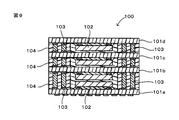
- the composite substrate 100 is formed by laminating and integrating a plurality of substrates 101a to 101d on which semiconductor elements 102 are mounted, and between adjacent substrates 101a to 101d is an interlayer connection conductor. They are connected via a columnar conductor 103.
- a thermosetting resin 104 is filled between the substrates, and each semiconductor element 102 and each columnar conductor 103 are resin-sealed.
- Each of the substrates 101a to 101d is made of ceramic, glass epoxy resin, or the like.
- the wiring formed on the composite substrate 100 and the arrangement of the semiconductor elements 102 have a three-dimensional structure, thereby enabling high-density mounting of components such as the semiconductor elements 102, and further, the substrates 101a to 101d.
- the composite substrate 100 is downsized by reducing the area of the main surface.
- the substrates 101a to 101d are being made thinner.
- the thickness of the substrates 101a to 101d formed of a hard material such as ceramic or glass epoxy resin is reduced, the rigidity of the substrates 101a to 101d is decreased.
- the substrates 101a to 101d may break due to shrinkage during curing.
- repulsive stress based on the warpage of the substrates 101a to 101d generated when the thermosetting resin 104 is cured and contracted concentrates on the connection portion between the substrates 101a to 101d and the columnar conductor 103, and thus the connection portion may be peeled off. There is also.
- thermosetting resin 104 in order to reduce the influence of curing shrinkage of the thermosetting resin 104, for example, when the substrate 101b is laminated on the lowermost substrate 101a, the thermosetting resin 104 on the substrate 101a is first placed. It is conceivable that the substrate 101b is disposed thereon after being cured (or semi-cured), and the substrate 101b is connected to the columnar conductor 103 with solder or the like. However, in such a case, the connection between the substrate 101b and the columnar conductor 103 requires strict flatness of the surface of the thermosetting resin 104 including the exposed end surface of the columnar conductor 103 and the substrate 101b.
- the present invention has been made in view of the above-described problems, and in a composite substrate formed by laminating a plurality of substrates, the substrate is thinned to achieve a low profile, and accompanying substrate cracks and columnar conductors
- the object is to prevent poor connection with the substrate.
- a composite substrate of the present invention includes a rigid substrate, a first sealing resin layer laminated on the rigid substrate, and a flexible substrate laminated on the first sealing resin layer. And a second sealing resin layer laminated on the flexible substrate, and a columnar conductor provided in the first sealing resin layer and connecting the rigid substrate and the flexible substrate. It is said.
- the flexible substrate can flexibly follow the shrinkage at the time of curing of both sealing resin layers, and when a hard substrate (rigid substrate) formed of a conventional ceramic or glass epoxy resin is thinned, It will not crack.
- the stress generated at this time is also distributed throughout the flexible substrate, the stress applied to the connecting portion between the columnar conductor and the flexible substrate can be reduced, and poor connection between the two can be prevented. it can. Accordingly, it is possible to reduce the height of the composite substrate, and to prevent the substrate (flexible substrate) from being cracked and the connection failure between the columnar conductor and the substrate.
- the flexible substrate may have a step.
- the flexible substrate is easy to form a step as compared with a rigid substrate formed of ceramic or glass epoxy resin. Therefore, by providing a step on the flexible substrate, an empty space in the composite substrate can be used effectively, and the degree of freedom in designing the composite substrate is improved. For example, when a plurality of components having different thicknesses in the stacking direction are arranged in each of the first sealing resin layer and the second sealing resin layer, a step is provided on the flexible substrate according to the height of each component. However, the mounting density of components can be improved by arranging the components at predetermined positions.
- the distance between predetermined wiring electrodes formed on the rigid substrate and the flexible substrate without changing the thickness of the composite substrate (thickness in the stacking direction), or the first sealing resin layer Since the distance between the component arranged in the second sealing resin layer and the component arranged in the second sealing resin layer can be increased, unnecessary stray capacitance generated between predetermined members provided in the composite substrate can be suppressed. it can.
- the first component disposed in the second sealing resin layer on the low-side region among the high-side region and the low-side region in the stacking direction of the flexible substrate formed by the step is provided.
- the thickness of the first component in the stacking direction may be larger than the thickness of the second sealing resin layer on the high-side region of the flexible substrate.
- the first component whose thickness in the stacking direction is thicker than the thickness of the second sealing resin layer on the high area of the flexible substrate is disposed in the low area of the flexible substrate formed by the steps.
- the height of the composite substrate can be reduced as compared with the case where the flexible substrate is formed in a flat plate shape with the entire surface being flat, and the first component is disposed on the second sealing resin layer on the flexible substrate. Can be planned.
- the flexible substrate may include a shield layer.
- the second component may be disposed on the first sealing resin layer and mounted on the rigid substrate, and the top surface of the second component may be in contact with the flexible substrate or the shield layer.
- the shielding performance of the second component is improved, and the heat dissipation characteristics of heat generated from the second component is improved.
- the distance between the rigid substrate and the flexible substrate can be narrowed, so that the height of the composite substrate can be reduced.
- a through hole is formed in the flexible substrate, and a third component is provided which is disposed in the first sealing resin layer and protrudes from the through hole toward the second sealing resin layer. Also good. Since the flexible substrate has flexibility, it is easier to process than a rigid substrate, and for example, a through hole can be easily formed by punching or the like. Accordingly, the through hole 12 is formed in the flexible substrate, and the third component is arranged by using the regions of the first sealing resin layer and the second sealing resin layer that communicate with each other through the through hole 12. It is possible to effectively utilize the empty space in the board. In addition, since the third component can be arranged by the through hole without increasing the distance between the rigid substrate and the flexible substrate, the composite substrate can be reduced in height and the components can be mounted at high density. .
- the flexible substrate may be formed of a thermoplastic resin.
- a flexible substrate can be easily formed by using a thermoplastic resin.
- the substrate constituting the composite substrate is a flexible substrate, even if the substrate is thinned in order to reduce the height of the composite substrate, it is flexible against shrinkage when the sealing resin layer is cured. Since the substrate can flexibly follow, it does not break as in the case where the hard substrate (rigid substrate) of the conventional composite substrate is thinned. In addition, since the stress generated at this time (at the time of curing shrinkage) is also distributed throughout the flexible substrate, the stress applied to the connecting portion between the columnar conductor and the flexible substrate can be reduced, and poor connection between the two can be prevented. it can. Accordingly, it is possible to reduce the height of the composite substrate, and to prevent the substrate (flexible substrate) from being cracked and the connection failure between the columnar conductor and the substrate.
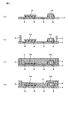
- FIG. 1A is a cross-sectional view of the composite substrate 1 (cross-sectional view taken along the line AA in FIGS. 1B and 1C), and FIG. FIG. 3C is a plan view of the rigid substrate 2 of the composite substrate 1, and FIG.
- a composite substrate 1 includes a rigid substrate 2, a first sealing resin layer 4 laminated on the rigid substrate 2, and the first sealing resin.
- a flexible substrate 3 laminated on the layer 4 a second sealing resin layer 5 laminated on the flexible substrate 3, and a rigid substrate 2 and a flexible substrate 3 provided in the first sealing resin layer 4.
- a columnar conductor 6 which is an interlayer connection conductor for connecting the two, for example, used for a high-frequency module such as a Wi-Fi module, a Bluetooth (registered trademark) module, or a switch module.
- the rigid substrate 2 is a substrate formed of a material harder than the flexible substrate 3 described later, and is formed of, for example, a low-temperature co-fired ceramic (LTCC) or a glass epoxy resin.
- LTCC low-temperature co-fired ceramic
- FIG. 1 (b) a plurality of components 7a1 and 7a2 are mounted on one main surface by using a known surface mounting technique, and the peripheral edges so as to surround each component 7a1 and 7a2.
- a plurality of columnar conductors 6 are mounted.
- a plurality of external electrodes 8 for external connection are formed on the other main surface.
- Each columnar conductor 6 may be a pin-shaped conductor formed by cutting a wire made of a metal such as Cu, or may be a via conductor.
- chip components such as IC (component 7a1) which is a semiconductor element formed with Si, GaAs, etc., a chip capacitor, a chip inductor, etc. are mentioned. Further, in this embodiment, as shown in FIG. 1A, the thickness in the stacking direction including the mounting electrodes of the component 7a1 is formed thinner than the thickness of the component 7a2.
- the components 7a1 and 7a2 and the columnar conductors 6 are covered with a first sealing resin layer 4 laminated on the rigid substrate 2.
- a thermosetting resin such as an epoxy resin can be used as the resin for forming the first sealing resin layer 4.
- the flexible substrate 3 is made of, for example, a thermoplastic resin such as liquid crystal polymer, polyimide, or polyetheretherketone, and wiring electrodes (not shown) are formed inside or on the surface thereof.
- a plurality of connection electrodes 9 for connection to the respective columnar conductors 6 are formed on the flexible substrate 3, and these connection electrodes 9 and the respective columnar conductors 6 are connected via solder or the like.
- a plurality of components 7b1 (chip components) and 7b2 (IC) each composed of an IC, a chip component such as a chip inductor and a chip capacitor are mounted on one main surface of the flexible substrate 3, and these components 7b1, 7 b 2 is covered with a second sealing resin layer 5 made of a thermosetting resin such as an epoxy resin laminated on the flexible substrate 3.
- the flexible substrate 3 is provided with a step utilizing the flexibility in order to effectively use the empty space in the composite substrate 1.
- each component 7b1, 7b2 corresponds to the first component of the present invention.
- the flexible substrate 3 is provided with a step in the stacking direction formed by bending, and the flexible substrate 3 formed by this step has a low-side region.
- Each component 7b1, 7b2 is mounted.
- this step is depressed in the region (empty space) on the component 7a1 which is the component having the smaller thickness in the stacking direction among the components 7a1 and 7a2 arranged in the first sealing resin layer 4.
- the components 7b1 and 7b2 whose thickness in the stacking direction is thicker than the thickness of the second sealing resin layer 5 on the high-side region of the flexible substrate 3 formed by the step are mounted in the low-side region. (H> h).
- a step is provided in the flexible substrate 3, and the second sealing resin layer 5 on the lower side region of the flexible substrate 3 formed by this step is used.
- the composite substrate 1 can be reduced in height.
- FIGS. 2 and 3 are explanatory views of the method of manufacturing the composite substrate 1.
- FIGS. 2 (a) to 2 (d) show respective steps
- FIGS. 3 (a) to 3 (c) show FIG. 2 (d). Each process following the process is shown.
- a rigid substrate 2 on which various wiring electrodes (not shown) and external electrodes 8 are formed is prepared.
- Components 7a1 and 7a2 are mounted.
- each pin-shaped columnar conductor 6 formed by cutting a wire made of a metal such as Cu is mounted on one main surface of the rigid substrate 2. At this time, one end of each columnar conductor 6 and the rigid substrate 2 are connected using solder or the like.
- thermosetting resin such as an epoxy resin is filled on one main surface of the rigid substrate 2 so as to cover the components 7a1 and 7a2 and the columnar conductors 6.
- 1 sealing resin layer 4 is formed.
- the 1st sealing resin layer 4 is made into a semi-hardened state.
- the first sealing resin layer 4 can be formed using a coating method, a printing method, a compression mold method, a transfer mold method, or the like.
- the surface of the first sealing resin layer 4 is pressed onto the surface of the first sealing resin layer 4 in a semi-cured state, whereby the surface of the first sealing resin layer 4 will be described later.
- the shape is suitable for
- a flexible substrate 3 is prepared on which each component 7b1, 7b2 is mounted on one main surface thereof.
- a flat flexible substrate 3 is prepared, and the step is bent by pressing the flexible substrate 3.
- the components 7b1 and 7b2 are mounted on the lower side region (recessed portion) of the flexible substrate 3 formed by the step using a known surface mounting technique.
- the flexible substrate 3 may be prepared before being disposed on the first sealing resin layer 4.
- the flexible substrate 3 is arranged at a predetermined position on the first sealing resin layer 4, and the connection electrode 9 of the flexible substrate 3 and the first sealing resin are arranged.
- the other end of the columnar conductor 6 exposed from the surface of the layer 4 is connected using solder.
- the connection electrode 9 is placed at a predetermined position (connection position of the corresponding columnar conductor 6) by utilizing the flexibility of the flexible substrate 3. Since it can arrange
- thermosetting resin such as an epoxy resin is applied so as to cover the components 7 b 1 and 7 b 2 mounted on the flexible substrate 3.
- the second sealing resin layer 5 is formed on the main surface, and the composite substrate 1 is manufactured.
- the resin of the first sealing resin layer 5 that is in a semi-cured state is completely cured at the same time as the resin of the second sealing resin layer 5 is cured.
- the second sealing resin layer 5 can also be formed by using a coating method, a printing method, a compression mold method, a transfer mold method, or the like.
- the manufacturing method of the above-mentioned composite substrate 1 forms the 1st sealing resin layer 4 and the 2nd sealing resin layer 5 separately, these resin layers 4 and 5 are formed collectively. You may make it do. In this case, after connecting each columnar conductor 6 and the connection electrode 9 of the flexible substrate 3, the first sealing resin layer 4 and the second sealing resin layer 5 are formed in a lump.
- each columnar conductor 6 may be formed of a via conductor.
- a via hole is formed in the first sealing resin layer 4 by laser processing or the like, and a conductive paste containing, for example, Ag, Cu, or the like is formed in the via hole. It is preferable to form a via conductor as the columnar conductor 6 by filling.
- the substrate laminated on the first sealing resin layer 4 is the flexible substrate 3.
- the flexible substrate 3 can flexibly follow the shrinkage of both the sealing resin layers 4 and 5 during curing, and is a substrate constituting a conventional composite substrate.
- the hard substrate (rigid substrate) formed of ceramic or glass epoxy resin is not cracked unlike the case where it is thinned.
- the stress generated at this time is also dispersed throughout the flexible substrate 3, the stress applied to the connection portion between each columnar conductor 6 and the flexible substrate 3 can be reduced, and the connection failure between them can be reduced. It can also be prevented.
- the flexible substrate 3 can be easily formed by using a thermoplastic resin as a material for forming the flexible substrate 3.
- the flexible substrate 3 is provided with a step in the stacking direction that is bent using the flexibility thereof, and the second sealing resin layer on the lower side region of the flexible substrate 3 formed by this step. 5, a plurality of components 7b1 and 7b2 whose thickness in the stacking direction is thicker than the thickness of the second sealing resin layer 5 on the high area of the flexible substrate 3 are arranged.
- the composite substrate 1 has a lower level. Can be turned upside down.
- the step of the flexible substrate 3 is a region on the IC (component 7a1) which is a component having a smaller thickness in the stacking direction among the components 7a1 and 7a2 arranged in the first sealing resin layer 4 ( Therefore, the thickness of the composite substrate 1 (the height in the stacking direction) does not increase due to the step.
- the empty space Since the space can be used effectively, the mounting density of each component 7a1, 7a2, 7b1, 7b2 on the composite substrate 1 can be improved.
- the step of the flexible substrate 3 when the step of the flexible substrate 3 is used, for example, the distance between predetermined wiring electrodes formed on the rigid substrate 2 and the flexible substrate 3 without changing the thickness of the composite substrate 1 (height in the stacking direction) Since the distance between the components 7a1 and 7a2 disposed in the first sealing resin layer 4 and the components 7b1 and 7b2 disposed in the second sealing resin layer 5 can be increased, the components 7a1 and 7a2 are provided in the composite substrate 1. Unnecessary stray capacitance generated between the predetermined members can be suppressed.
- step difference for utilizing effectively the empty space in the composite substrate 1 can be formed easily, and, thereby, the design of the composite substrate 1 is carried out.
- the degree of freedom is improved.
- each columnar conductor 6 and the flexible substrate 3 when connecting each columnar conductor 6 and the flexible substrate 3, the surface of the first sealing resin layer 4 including the exposed end surface of each columnar conductor 6, and each columnar conductor 6, as in a conventional composite substrate. It is not necessary to ensure the strict flatness of the substrate connected to each other, and each columnar conductor 6 and each connection terminal 9 can be reliably connected by utilizing the flexibility of the flexible substrate 3, so that it is easy to combine them.
- the substrate 1 can be manufactured.
- the material for forming the flexible substrate 3 is a liquid crystal polymer and the material for forming the first and second sealing resin layers 4 and 5 is formed of a thermosetting epoxy resin, it is generally used for industrial products. Since the flexible substrate 3 and the both sealing resin layers 4 and 5 can be formed of a simple material, it is practical.
- FIG. 4 is a cross-sectional view of the composite substrate 1a.
- the composite substrate 1a according to this embodiment differs from the composite substrate 1 of the first embodiment described with reference to FIG. 1 in that the flexible substrate 3 includes a shield layer 11 as shown in FIG. . Since the other configuration is the same as that of the composite substrate 1 of the first embodiment, description thereof is omitted by attaching the same reference numerals.
- the flexible substrate 3 is provided with a shield layer 11 formed of a metal foil such as Cu.
- the thermoplastic resin forming the flexible substrate 3 in this embodiment has a higher adhesion strength to the Cu foil than the ceramic forming the substrate of the conventional composite substrate, and thus forms the shield layer 11 having a large area in plan view. Easy to do. Therefore, by forming the shield layer 11 having a large area (area in plan view) on the flexible substrate 3 between the first sealing resin layer 4 and the second sealing resin layer 5, the first sealing resin layer 4 is formed. Mutual interference of unnecessary electromagnetic waves generated from the components 7a1 and 7a2 disposed in the stop resin layer 4 and the components 7b1 and 7b2 disposed in the second sealing resin layer 5 can be prevented.
- the shield layer 11 also improves the heat dissipation characteristics of heat generated from the composite substrate 1. In addition, about the shape and arrangement
- FIG. The shield layer 11 may be provided either on the surface of the flexible substrate 3 or inside. Moreover, the above-mentioned flexible substrate 3 and the shield layer 11 can also use a commercially available resin sheet with copper foil.
- FIG. 5 is a cross-sectional view of the composite substrate 1b.
- the composite substrate 1b according to this embodiment differs from the composite substrate 1a of the second embodiment described with reference to FIG. 4 in that no step is provided on the flexible substrate 3, as shown in FIG.
- the through-hole 12 is formed in the flexible substrate 3, and the component 7a3 (corresponding to the third component of the present invention) arranged in the first sealing resin layer 4 is connected to the second sealing resin layer 5 side from the through-hole 12 It is the point which is provided protruding. Since the other configuration is the same as that of the composite substrate 1a of the second embodiment, description thereof is omitted by attaching the same reference numerals.
- the through holes 12 are formed at predetermined positions of the flat flexible substrate 3 by punching or the like, and are arranged in the first sealing resin layer 4 so that the thickness in the stacking direction is the rigid substrate 2 and the flexible substrate 3.
- a part 7a3 that is thicker than the gap between the through hole 12 and the second sealing resin layer 5 is provided.
- the flexible substrate 3 Since the flexible substrate 3 has flexibility, it is easier to process than the rigid substrate 2, and the through holes 12 can be easily formed by the above-described punching or the like. Therefore, instead of providing a step in the flexible substrate 3, the through hole 12 is formed, and the component 7 a 3 is disposed in the region of the first sealing resin layer 4 and the second sealing resin layer 5 communicated by the through hole 12. Thus, the empty space in the composite substrate 1b can be effectively used. Further, since the component 7a3 can be disposed by the through-hole 12 without increasing the distance between the rigid substrate 2 and the flexible substrate 3, the height of the composite substrate 1b can be reduced, and the components 7a1, 7a3, 7b1, 7b2 high-density mounting can be achieved.
- the notch is formed by providing a notch in the peripheral portion of the flexible substrate 3. You may make it make the 1st sealing resin layer 4 and the 2nd sealing resin layer 5 connect by a notch. If it does in this way, the freedom degree of arrangement of parts 7a3 will improve.
- FIG. 6 is a cross-sectional view of the composite substrate 1c.
- the composite substrate 1c according to this embodiment is different from the composite substrate 1a of the second embodiment described with reference to FIG. 4 in that another composite substrate 1c is formed on the second sealing resin layer 5 as shown in FIG. A point in which the rigid substrate 2a is laminated, a point in which a plurality of columnar conductors 6a for connecting the rigid substrate 2a and the flexible substrate 3 are disposed on the second sealing resin layer 5, and a second sealing Of the components 7b1 and 7b2 arranged on the resin layer 5, one component 7b2 is mounted on the rigid substrate 2a, and only the portion of the flexible substrate 3 corresponding to the components 7a1 and 7b2 that are ICs is shielded.
- the layer 11 is provided. Since the other configuration is the same as that of the composite substrate 1a of the second embodiment, description thereof is omitted by attaching the same reference numerals.
- the design flexibility of the wiring electrode formed inside the composite substrate 1c is increased. improves.
- the thickness in the stacking direction is formed on the main surface on the second sealing resin layer 5 side of the rigid substrate 2a on the high-side region of the flexible substrate 3 formed by steps.
- each component 7a1, 7a2 between the sealing resin layers 4, 5 is provided.
- 7b1 and 7b2 can be effectively prevented from mutual interference with each other, and the formation area of the shield layer 11 can be reduced to reduce the manufacturing cost of the flexible substrate 3.
- the components 7a1 and 7b2 are heat radiating components such as power amplifiers, the heat generated in the components 7a1 and 7b2 is transmitted from the shield layer 11 to the flexible substrate 3 and further from the end surface exposed portion on the side surface of the composite substrate 1c of the flexible substrate 3. It can escape to the outside, and the heat dissipation of the composite substrate 1c can be improved.
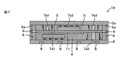
- FIG. 7 is a cross-sectional view of the composite substrate 1d.
- the composite substrate 1d according to this embodiment is different from the composite substrate 1c of the fourth embodiment described with reference to FIG. 6 in that no step is provided on the flexible substrate 3 as shown in FIG. And all the components 7b1, 7b2, 7b3 arranged in the second sealing resin layer 5 are mounted on the main surface on the second sealing resin layer 5 side of the upper rigid substrate 2a, and these The components 7b1, 7b2, and 7b3 are disposed in contact with the flexible substrate 3, and the component 7a2 disposed in the first sealing resin layer 4 is disposed in contact with the flexible substrate 3. Is a point. Since the other configuration is the same as that of the composite substrate 1c of the fourth embodiment, description thereof is omitted by attaching the same reference numerals.
- the flexible substrate 3 is disposed on the first sealing resin layer 4 and the components 7a1, 7a2, and the second It functions as an insulating layer that prevents conduction between the components 7b1, 7b2, and 7b3 disposed in the sealing resin layer 5.
- positioned at the 2nd sealing resin layer 5 can be made small. Therefore, it is possible to reduce the height of the composite substrate 1d.
- FIG. 8 is a cross-sectional view of the composite substrate 1e.
- the composite substrate 1e according to this embodiment differs from the composite substrate 1d of the fifth embodiment described with reference to FIG. 7 in that the composite substrate 1e is disposed in the first sealing resin layer 4 as shown in FIG.
- the top surface of the component 7 a 1 is in contact with the shield layer 11 provided on the flexible substrate 3. Since other configurations are the same as those of the composite substrate 1d of the fifth embodiment, the description thereof is omitted by giving the same reference numerals.
- the shielding property of the component 7a1 is further improved and the heat generated from the component 7a1 is increased. Heat dissipation is also improved.
- the composite substrate 1e can be reduced in height.
- the parts 7a1 and 7a2 correspond to the second part of the present invention.
- each component 7b is mounted on the main surface of the flexible substrate 3 on the second sealing resin layer 5 side.
- the first sealing resin layer 4 of the flexible substrate 3 is described. Even if it is the structure which mounts components in the main surface of the side.
- the present invention can be applied to various composite substrates formed by laminating a plurality of substrates on which components are mounted.
Landscapes
- Engineering & Computer Science (AREA)
- Microelectronics & Electronic Packaging (AREA)
- Manufacturing & Machinery (AREA)
- Production Of Multi-Layered Print Wiring Board (AREA)
- Non-Metallic Protective Coatings For Printed Circuits (AREA)
- Structure Of Printed Boards (AREA)
- Combinations Of Printed Boards (AREA)
Abstract
複数の基板が積層されて成る複合基板において、基板の薄型化により低背化を図るとともに、これに伴う基板の割れや柱状導体と基板との接続不良を防止する。 複合基板(1)は、リジッド基板(2)と、該リジッド基板(2)に積層された第1の封止樹脂層(4)と、該第1の封止樹脂層(4)に積層されたフレキシブル基板(3)と、該フレキシブル基板(3)に積層された第2の封止樹脂層(5)と、第1の封止樹脂層(4)内に設けられ、リジッド基板(2)とフレキシブル基板(3)とを接続する柱状導体(6)とを備える。これにより、複合基板(1)の低背化を図るためにフレキシブル基板(3)を薄くした場合であっても、第1および第2の封止樹脂層(4,5)の硬化時の熱収縮によりフレキシブル基板(3)が割れることがない。また、フレキシブル基板(3)の柔軟性により、柱状導体(6)とフレキシブル基板(3)との接続部にかかる応力が緩和されるため、両者の接続不良を防止することができる。
Description
本発明は、部品が実装された複数の基板が積層されて成る複合基板に関する。
携帯電話等の携帯端末装置の小型化に伴って、これに搭載される電子装置の小型化が進められている。この種の電子装置の一例として、従来では、それぞれ主面に半導体素子などの部品を実装した複数の基板を積層して一体化した複合基板が提案されている(特許文献1参照)。
この複合基板100は、図9に示すように、それぞれ、半導体素子102を実装した複数の基板101a~101dを積層して一体化したものであり、隣接する基板101a~101d間が層間接続導体である柱状導体103を介して接続される。また、基板間には熱硬化性樹脂104が充填されて、各半導体素子102および各柱状導体103が樹脂封止される。なお、各基板101a~101dは、セラミックやガラスエポキシ樹脂などで形成されている。このように、複合基板100に形成される配線や各半導体素子102の配置を立体的な構造にすることで、半導体素子102等の部品の高密度実装化を可能にし、さらに、基板101a~101dの主面の面積を小さくして複合基板100の小型化が図られている。
このような複合基板100の小型化の一貫として、近年、複合基板100の低背化も要求されており、その手段として、基板101a~101dの薄型化が進められている。しかしながら、上記した複合基板100において、セラミックやガラスエポキシ樹脂などの硬い材料で形成された基板101a~101dの厚みを薄くすると、基板101a~101dの剛性が低くなり、例えば、熱硬化性樹脂104の硬化時の収縮により、基板101a~101dが割れるおそれがある。また、熱硬化性樹脂104の硬化収縮時に発生する基板101a~101dの反りに基づく反発応力が、基板101a~101dと柱状導体103との接続部に集中するため、この接続部で剥がれが生じるおそれもある。
これらの問題の対策として、熱硬化性樹脂104の硬化収縮の影響を低減するために、例えば、最下層の基板101a上に基板101bを積層する際、基板101a上の熱硬化性樹脂104を先に硬化(または、半硬化)させてからその上に基板101bを配置し、該基板101bを柱状導体103に半田などにより接続させることが考えられる。しかし、このような場合には、基板101bと柱状導体103との接続に、露出した柱状導体103の端面を含む熱硬化性樹脂104の表面や基板101bの厳格な平坦性が要求されるため、柱状導体103の高さのばらつきや、基板101b自体の反りなどを考慮すると、依然、基板101bと柱状導体103との接続不良のおそれがある。この点、両者を接続する半田の量を増やして基板101bの反りや柱状導体103の高さのばらつきを吸収することも考えられるが、柱状導体103が狭ピッチで配置される近年の複合基板では、隣接する柱状導体103同士が短絡するおそれがある。
本発明は、上記した課題に鑑みてなされたものであり、複数の基板が積層されて成る複合基板において、基板の薄型化により低背化を図るとともに、これに伴う基板の割れや柱状導体と基板との接続不良を防止することを目的とする。
上記した目的を達成するために、本発明の複合基板は、リジッド基板と、前記リジッド基板に積層された第1の封止樹脂層と、前記第1の封止樹脂層に積層されたフレキシブル基板と、前記フレキシブル基板に積層された第2の封止樹脂層と、前記第1の封止樹脂層内に設けられ、前記リジッド基板と前記フレキシブル基板とを接続する柱状導体とを備えることを特徴としている。
このように、第1の封止樹脂層に積層される基板をフレキシブル基板にすることで、例えば、複合基板の低背化を図るために、フレキシブル基板の厚みを薄くした場合であっても、両封止樹脂層の硬化時の収縮に対して当該フレキシブル基板が柔軟に追従することができ、従来のセラミックやガラスエポキシ樹脂で形成された硬い基板(リジッド基板)を薄くした場合のように、割れることがない。また、このとき(硬化収縮時)に発生する応力もフレキシブル基板全体に分散するため、柱状導体とフレキシブル基板との接続部にかかる応力を低減することができ、両者の接続不良を防止することもできる。したがって、複合基板の低背化を図ることができるとともに、これに伴う基板(フレキシブル基板)の割れや柱状導体と基板との接続不良を防止することができる。
また、前記フレキシブル基板が、段差を有していてもよい。フレキシブル基板は、セラミックやガラスエポキシ樹脂で形成されたリジッド基板と比較して、段差を形成するのが容易である。したがって、フレキシブル基板に段差を設けることで複合基板内の空きスペースを有効活用することができ、複合基板の設計自由度が向上する。例えば、第1の封止樹脂層および第2の封止樹脂層それぞれに、積層方向の厚みが異なる複数の部品を配置する場合には、フレキシブル基板に各部品の高さに応じて段差を設けつつ、所定位置に各部品を配置することで部品の実装密度の向上を図ることができる。また、例えば、段差を設けることにより、複合基板の厚み(積層方向の厚み)を変えずに、リジッド基板およびフレキシブル基板に形成された所定の配線電極間の距離や、第1の封止樹脂層に配置された部品と第2の封止樹脂層に配置された部品との距離を離すことができるため、複合基板内に設けられた所定の部材間に発生する不要な浮遊容量を抑えることもできる。
また、前記段差により形成された前記フレキシブル基板の積層方向の高所側領域と低所側領域のうち、前記低所側領域上の前記第2の封止樹脂層に配置された第1部品を備え、前記第1部品の積層方向の厚みが、前記フレキシブル基板の前記高所側領域上の前記第2の封止樹脂層の厚みよりも厚くなるようにしてもよい。
このように、段差により形成されたフレキシブル基板の低所側領域に、その積層方向の厚みがフレキシブル基板の高所領域上の第2の封止樹脂層の厚みよりも厚い第1部品を配置することで、フレキシブル基板をその全面が平坦な平板状に形成し、該フレキシブル基板の上層の第2の封止樹脂層に第1部品を配置する場合と比較して、複合基板の低背化を図ることができる。
また、前記フレキシブル基板が、シールド層を備えていてもよい。このようにすることで、第1の封止樹脂層に配置される部品および第2の封止樹脂層に配置される部品から発生する不要な電磁波の相互干渉を防止することができる。また、複合基板から発生する熱の放熱特性も向上する。
また、前記第1の封止樹脂層に配置され、前記リジッド基板に実装された第2部品を備え、前記第2部品の天面が前記フレキシブル基板又は前記シールド層に接していてもよい。例えば、第2部品がシールド層に接している場合は、第2部品のシールド性が向上するとともに、第2部品から発生する熱の放熱特性が向上する。また、フレキシブル基板に接している場合は、リジッド基板とフレキシブル基板との間隔を狭くすることができるため、複合基板の低背化を図ることができる。
前記フレキシブル基板に貫通孔が形成されており、前記第1の封止樹脂層に配置され、前記貫通孔から前記第2の封止樹脂層側に突出して設けられた第3部品を備えていてもよい。フレキシブル基板は柔軟性を有するため、リジッド基板と比較して加工し易く、例えばパンチ加工などにより容易に貫通孔を形成することができる。したがって、フレキシブル基板に貫通孔12を形成し、該貫通孔12により連通した第1の封止樹脂層および第2の封止樹脂層の領域を利用して第3部品を配置することで、複合基板内の空きスペースを有効活用することができる。また、当該貫通孔により、リジッド基板とフレキシブル基板との間隔を広げることなく第3部品を配置することができるため、複合基板の低背化、並びに、部品の高密度実装化を図ることができる。
また、前記フレキシブル基板が、熱可塑性樹脂で形成されていてもよい。このように、熱可塑性樹脂を用いることで、容易にフレキシブル基板を形成することができる。
本発明によれば、複合基板を構成する基板をフレキシブル基板とすることで、複合基板の低背化を図るために基板を薄くしても、封止樹脂層の硬化時の収縮に対してフレキシブル基板が柔軟に追従することができるため、従来の複合基板の硬い基板(リジッド基板)を薄くした場合のように、割れることがない。また、このとき(硬化収縮時)に発生する応力もフレキシブル基板全体に分散するため、柱状導体とフレキシブル基板との接続部にかかる応力を低減することができ、両者の接続不良を防止することもできる。したがって、複合基板の低背化を図ることができるとともに、これに伴う基板(フレキシブル基板)の割れや柱状導体と基板との接続不良を防止することができる。
<第1実施形態>
本発明の第1実施形態にかかる複合基板について、図1を参照して説明する。なお、図1は第1実施形態にかかる複合基板1の説明図であり、(a)は複合基板1の断面図((b)および(c)におけるA-A断面図)、(b)は複合基板1のリジッド基板2の平面図、(c)は複合基板1のフレキシブル基板3の平面図である。
本発明の第1実施形態にかかる複合基板について、図1を参照して説明する。なお、図1は第1実施形態にかかる複合基板1の説明図であり、(a)は複合基板1の断面図((b)および(c)におけるA-A断面図)、(b)は複合基板1のリジッド基板2の平面図、(c)は複合基板1のフレキシブル基板3の平面図である。
この実施形態にかかる複合基板1は、図1(a)に示すように、リジッド基板2と、該リジッド基板2に積層された第1の封止樹脂層4と、該第1の封止樹脂層4に積層されたフレキシブル基板3と、該フレキシブル基板3に積層された第2の封止樹脂層5と、第1の封止樹脂層4内に設けられ、リジッド基板2とフレキシブル基板3とを接続する層間接続導体である柱状導体6とを備え、例えば、Wi-Fi用モジュール、Bluetooth(登録商標)用モジュール、スイッチモジュールなどの高周波系のモジュールに使用される。
リジッド基板2は、後述するフレキシブル基板3よりも硬い材料で形成された基板であり、例えば、低温同時焼成セラミック(LTCC)やガラスエポキシ樹脂などで形成される。そして、図1(b)に示すように、その一方主面には、複数の部品7a1,7a2が周知の表面実装技術を用いて実装されるとともに、各部品7a1,7a2を囲むように、周縁に複数の柱状導体6が実装される。また、他方主面には、外部接続用の複数の外部電極8が形成される。なお、各柱状導体6は、Cuなどの金属からなる線材を切断加工して形成されたピン状の導体であってもよいし、ビア導体であってもよい。また、各部品7a1,7a2としては、SiやGaAsなどで形成された半導体素子であるIC(部品7a1)や、チップコンデンサ、チップインダクタなどのチップ部品(部品7a2)が挙げられる。また、この実施形態では、図1(a)に示すように、部品7a1の実装用電極を含めた積層方向の厚みは、部品7a2の厚みより薄く形成されている。
また、各部品7a1,7a2および各柱状導体6は、リジッド基板2に積層された第1の封止樹脂層4により被覆されている。なお、第1の封止樹脂層4を形成する樹脂として、エポキシ樹脂などの熱硬化性樹脂を用いることができる。
フレキシブル基板3は、例えば、液晶ポリマ、ポリイミド、ポリエーテルエーテルケトンなどの熱可塑性樹脂からなり、その内部や表面に配線電極(図示せず)が形成される。また、フレキシブル基板3には、各柱状導体6との接続用の複数の接続電極9が形成され、これらの接続電極9と各柱状導体6とが半田などを介して接続される。
また、フレキシブル基板3の一方主面には、それぞれICや、チップインダクタ、チップコンデンサなどのチップ部品等から成る複数の部品7b1(チップ部品),7b2(IC)が実装され、これらの部品7b1,7b2が、フレキシブル基板3に積層されたエポキシ樹脂などの熱硬化性樹脂からなる第2の封止樹脂層5により被覆される。このとき、フレキシブル基板3には、複合基板1内の空きスペースを有効活用するために、その柔軟性を利用した段差が設けられている。なお、この実施形態では、各部品7b1,7b2が本発明の第1部品に相当する。
具体的には、図1(a)に示すように、フレキシブル基板3には、屈曲形成された積層方向の段差が設けられており、この段差により形成されたフレキシブル基板3の低所側領域に各部品7b1,7b2が実装される。このとき、この段差は、第1の封止樹脂層4に配置された各部品7a1,7a2のうち、その積層方向の厚みが薄い方の部品である部品7a1上の領域(空きスペース)に窪んで設けられる。そして、この段差により形成されたフレキシブル基板3の高所側領域上の第2の封止樹脂層5の厚みよりも、その積層方向の厚みが厚い部品7b1,7b2が低所側領域に実装される(H>h)。このように、複合基板1内の空きスペースを利用して、フレキシブル基板3に段差を設け、この段差により形成されたフレキシブル基板3の低所側領域上の第2の封止樹脂層5に、積層方向の厚みが厚い部品7b1,7b2を配置することで、複合基板1の低背化が可能になる。
(複合基板の製造方法)
次に、複合基板1の製造方法について、図2および図3を参照して説明する。なお、図2および図3は、複合基板1の製造方法の説明図であり、図2(a)~(d)はその各工程、図3(a)~(c)は図2(d)の工程に続く各工程を示す。
次に、複合基板1の製造方法について、図2および図3を参照して説明する。なお、図2および図3は、複合基板1の製造方法の説明図であり、図2(a)~(d)はその各工程、図3(a)~(c)は図2(d)の工程に続く各工程を示す。
まず、図2(a)に示すように、各種の配線電極(図示せず)や外部電極8が形成されたリジッド基板2を用意し、その一方主面に周知の表面実装技術を用いて各部品7a1,7a2を実装する。
次に、図2(b)に示すように、それぞれCuなどの金属からなる線材を切断加工して形成されたピン状の各柱状導体6を、リジッド基板2の一方主面に実装する。このとき、各柱状導体6の一端とリジッド基板2とを半田などを用いて接続する。
次に、図2(c)に示すように、各部品7a1,7a2および各柱状導体6を被覆するように、エポキシ樹脂などの熱硬化性樹脂をリジッド基板2の一方主面に充填して第1の封止樹脂層4を形成する。このとき、第1の封止樹脂層4を半硬化状態にする。なお、第1の封止樹脂層4は、塗布方式、印刷方式、コンプレッションモールド方式、トランスファモールド方式などを用いて形成することができる。なお、各柱状導体6の他端が第1の封止樹脂層4の表面から露出していない場合は、各柱状導体6の他端を第1の封止樹脂層4の表面から露出させるように、第1の封止樹脂層4の表面を研磨または研削する。
次に、図2(d)に示すように、半硬化状態の第1の封止樹脂層4の表面をプレスすることにより、第1の封止樹脂層4の表面を、後述するフレキシブル基板3に合った形状に形成する。
次に、図3(a)に示すように、各部品7b1,7b2がその一方主面に実装されたフレキシブル基板3を準備する。このとき、まず、平板状のフレキシブル基板3を用意し、このフレキシブル基板3をプレスするなどして、段差を屈曲形成する。そして、この段差により形成されたフレキシブル基板3の低所側領域(窪んだ部分)に、各部品7b1,7b2を周知の表面実装技術を用いて実装する。なお、当該フレキシブル基板3は、第1の封止樹脂層4上に配置する前までに準備しておけばよい。
次に、図3(b)に示すように、フレキシブル基板3を第1の封止樹脂層4上の所定の位置に配置して、フレキシブル基板3の接続電極9と、第1の封止樹脂層4の表面から露出した柱状導体6の他端とを半田を用いて接続する。なお、従来の複合基板のように、フレキシブル基板3に代えてリジッド基板を用いた場合、接続電極9と柱状導体6との接続に、柱状導体6の他端を含む第1の封止樹脂層4の表面およびリジッド基板の厳格な平坦性が要求されるが、この実施形態では、フレキシブル基板3の柔軟性を利用して、接続電極9を所定位置(対応する柱状導体6の接続位置)に容易に配置することができるため、上記した厳格な平坦性を確保する必要がない。
次に、図3(c)に示すように、フレキシブル基板3に実装された各部品7b1,7b2を被覆するように、エポキシ樹脂などの熱硬化性樹脂を塗布するなどして、フレキシブル基板3の一方主面上に第2の封止樹脂層5を形成し、複合基板1を製造する。このとき、第2の封止樹脂層5の樹脂を硬化させるのと同時に、半硬化状態であった、第1の封止樹脂層の樹脂を完全に硬化させる。この第2の封止樹脂層5も、第1の封止樹脂層4と同様に、塗布方式、印刷方式、コンプレッションモールド方式、トランスファモールド方式などを用いて形成することができる。
なお、上記した複合基板1の製造方法は、第1の封止樹脂層4と第2の封止樹脂層5とを別々に形成しているが、これらの樹脂層4,5を一括で形成するようにしてもよい。この場合、各柱状導体6とフレキシブル基板3の接続電極9とを接続させた後に、一括で第1の封止樹脂層4および第2の封止樹脂層5を形成する。
また、各柱状導体6をビア導体で形成してもよい。この場合、第1の封止樹脂層4を形成した後に、第1の封止樹脂層4に、レーザ加工などでビアホールを形成し、このビアホールに、例えば、AgやCuなどを含む導体ペーストを充填して柱状導体6としてのビア導体を形成するとよい。
したがって、上記した実施形態によれば、第1の封止樹脂層4に積層される基板をフレキシブル基板3にすることで、例えば、複合基板1の低背化を図るために、フレキシブル基板3の厚みを薄くした場合であっても、両封止樹脂層4,5の硬化時の収縮に対して、当該フレキシブル基板3が柔軟に追従することができ、従来の複合基板を構成する基板である、セラミックやガラスエポキシ樹脂で形成された硬い基板(リジッド基板)を薄くした場合のように、割れることがない。また、このとき(硬化収縮時)に発生する応力もフレキシブル基板3全体に分散するため、各柱状導体6とフレキシブル基板3との接続部にかかる応力を低減することができ、両者の接続不良を防止することもできる。したがって、複合基板1の低背化を図ることができるとともに、これに伴う基板(フレキシブル基板3)の割れや各柱状導体6とフレキシブル基板3との接続不良を防止することができる。また、フレキシブル基板3を形成する材料として熱可塑性樹脂を用いることで、容易にフレキシブル基板3を形成することができる。
また、フレキシブル基板3には、その柔軟性を利用して屈曲形成された積層方向の段差が設けられ、この段差により形成されたフレキシブル基板3の低所側領域上の第2の封止樹脂層5に、その積層方向における厚みが、フレキシブル基板3の高所側領域上の第2の封止樹脂層5の厚みよりも厚い複数の部品7b1,7b2が配置される。このように、フレキシブル基板3の低所側領域に、高所側領域上の第2の封止樹脂層5の厚みよりも、その積層方向の厚みが厚い部品7b1,7b2を配置することで、例えば、フレキシブル基板3をその全面が平坦な平板状に形成した上で、その上層の第2の封止樹脂層5に各部品7b1,7b2を配置する場合と比較して、複合基板1の低背化を図ることができる。
また、フレキシブル基板3の段差は、第1の封止樹脂層4に配置された各部品7a1,7a2のうち、その積層方向の厚みが薄い方の部品であるIC(部品7a1)上の領域(空きスペース)に窪んで設けられるため、この段差により、複合基板1の厚み(積層方向の高さ)が厚くなることはない。換言すれば、複合基板1内の空きスペースに、フレキシブル基板3の段差を設けつつ、この段差により形成されたフレキシブル基板3の低所側領域に各部品7b1,7b2を配置することで、当該空きスペースを有効活用することができるため、複合基板1における各部品7a1,7a2,7b1,7b2の実装密度の向上を図ることができる。
また、フレキシブル基板3の段差を利用すると、複合基板1の厚み(積層方向の高さ)を変えずに、例えば、リジッド基板2およびフレキシブル基板3それぞれに形成された所定の配線電極間の距離や、第1の封止樹脂層4に配置された部品7a1,7a2と第2の封止樹脂層5に配置された部品7b1,7b2との距離を離すこともできるため、複合基板1内に設けられた所定の部材間に発生する不要な浮遊容量を抑えることができる。このように、複合基板1が備える基板をフレキシブル基板3とすることで、複合基板1内の空きスペースを有効活用するための段差を容易に形成することができ、これにより、複合基板1の設計自由度が向上する。
また、各柱状導体6とフレキシブル基板3との接続に当たり、従来の複合基板のように、各柱状導体6の露出した端面を含む第1の封止樹脂層4の表面、および、各柱状導体6に接続される基板の厳格な平坦性を確保する必要がなく、フレキシブル基板3の柔軟性を利用して確実に各柱状導体6と各接続端子9とを接続させることができるため、容易に複合基板1を製造することができる。
また、フレキシブル基板3を形成する材料を液晶ポリマとし、第1および第2の封止樹脂層4,5を形成する材料を熱硬化性のエポキシ樹脂で形成する場合、工業製品に用いられる一般的な材料でフレキシブル基板3および両封止樹脂層4,5を形成することができるため実用的である。
<第2実施形態>
本発明の第2実施形態にかかる複合基板1aについて、図4を参照して説明する。なお、図4は複合基板1aの断面図である。
本発明の第2実施形態にかかる複合基板1aについて、図4を参照して説明する。なお、図4は複合基板1aの断面図である。
この実施形態にかかる複合基板1aが、図1を参照して説明した第1実施形態の複合基板1と異なるところは、図4に示すように、フレキシブル基板3がシールド層11を備える点である。その他の構成は、第1実施形態の複合基板1と同じであるため、同一符号を付すことにより説明を省略する。
この場合、フレキシブル基板3に、Cuなどの金属箔で形成されたシールド層11が設けられる。この実施形態におけるフレキシブル基板3を形成する熱可塑性樹脂は、従来の複合基板の基板を形成するセラミックよりも、Cu箔との密着強度が高いため、平面視での面積が大きいシールド層11を形成するのが容易である。したがって、第1の封止樹脂層4と第2の封止樹脂層5との間のフレキシブル基板3に面積(平面視での面積)が大きいシールド層11を形成することで、第1の封止樹脂層4に配置された各部品7a1,7a2および第2の封止樹脂層5に配置された各部品7b1,7b2から発生する不要な電磁波の相互干渉を防止することができる。また、このシールド層11により、複合基板1から発生する熱の放熱特性も向上する。なお、シールド層11の形状や配置については、両封止樹脂層4,5の各部品7a1,7a2,7b1,7b2の大きさや配置に応じて適宜変更するとよい。また、シールド層11は、フレキシブル基板3の表面および内部のいずれに設けてもよい。また、上述のフレキシブル基板3とシールド層11は、市販の銅箔付の樹脂シートを用いることもできる。
<第3実施形態>
本発明の第3実施形態にかかる複合基板1bについて、図5を参照して説明する。なお、図5は複合基板1bの断面図である。
本発明の第3実施形態にかかる複合基板1bについて、図5を参照して説明する。なお、図5は複合基板1bの断面図である。
この実施形態にかかる複合基板1bが、図4を参照して説明した第2実施形態の複合基板1aと異なるところは、図5に示すように、フレキシブル基板3に段差が設けられていない点、フレキシブル基板3に貫通孔12が形成され、第1の封止樹脂層4に配置された部品7a3(本発明の第3部品に相当)が当該貫通孔12から第2の封止樹脂層5側に突出して設けられている点である。その他の構成は、第2実施形態の複合基板1aと同じであるため、同一符号を付すことにより説明を省略する。
この場合、平板状のフレキシブル基板3の所定位置に貫通孔12がパンチ加工などにより形成され、第1の封止樹脂層4に配置された、その積層方向の厚みがリジッド基板2とフレキシブル基板3との間隔よりも厚い部品7a3が、当該貫通孔12から第2の封止樹脂層5側に突出して設けられる。
フレキシブル基板3は柔軟性を有するため、リジッド基板2と比較して加工し易く、上記したパンチ加工などにより容易に貫通孔12を形成することができる。したがって、フレキシブル基板3に段差を設ける代わりに貫通孔12を形成し、該貫通孔12により連通した第1の封止樹脂層4および第2の封止樹脂層5の領域に部品7a3を配置することで、複合基板1b内の空きスペースを有効活用することができる。また、当該貫通孔12により、リジッド基板2とフレキシブル基板3との間隔を広げることなく部品7a3を配置することができるため、複合基板1bの低背化、並びに、各部品7a1,7a3,7b1,7b2の高密度実装化を図ることができる。なお、第1の封止樹脂層4と第2の封止樹脂層5とを連通させる場所は適宜変更可能であり、例えば、フレキシブル基板3の周縁部に切欠きを設けるなどして、この切欠きにより、第1の封止樹脂層4と第2の封止樹脂層5とを連通させるようにしてもよい。このようすると、部品7a3の配置の自由度が向上する。
<第4実施形態>
本発明の第4実施形態にかかる複合基板1cについて、図6を参照して説明する。なお、図6は、複合基板1cの断面図である。
本発明の第4実施形態にかかる複合基板1cについて、図6を参照して説明する。なお、図6は、複合基板1cの断面図である。
この実施形態にかかる複合基板1cが、図4を参照して説明した第2実施形態の複合基板1aと異なるところは、図6に示すように、第2の封止樹脂層5上に他のリジッド基板2aが積層されている点と、第2の封止樹脂層5に当該リジッド基板2aとフレキシブル基板3とを接続する複数の柱状導体6aが配置されている点と、第2の封止樹脂層5に配置された各部品7b1,7b2のうちの1つの部品7b2がリジッド基板2aに実装されている点と、フレキシブル基板3において、ICである部品7a1,7b2に対応する部分にのみシールド層11が設けられている点である。その他の構成は、第2実施形態の複合基板1aと同じであるため、同一符号を付すことにより説明を省略する。
このように、各柱状導体6aでフレキシブル基板3に接続されたリジッド基板2aを、第2の封止樹脂層5に積層することで、複合基板1cの内部に形成する配線電極の設計自由度が向上する。また、図6に示すように、このリジッド基板2aの第2の封止樹脂層5側の主面に、その積層方向の厚みが、段差により形成されたフレキシブル基板3の高所側領域上の第2の封止樹脂層5の厚みよりも厚い部品7b2を実装する場合には、フレキシブル基板3の低所側領域に配置することで、複合基板1cの低背化を図ることができる。
また、シールド層11が、不要な電磁波によって特性が変わり易いIC(部品7a1,部品7b2)に対応する箇所のみに設けられているため、両封止樹脂層4,5間の各部品7a1,7a2,7b1,7b2の不要な電磁波の相互干渉を効果的に防止することができるとともに、シールド層11の形成領域を小さくしてフレキシブル基板3の製造コストの低減を図ることができる。さらに、部品7a1,7b2が電力増幅器などの放熱部品の場合、部品7a1,7b2で発生した熱をシールド層11からフレキシブル基板3へ伝え、さらにフレキシブル基板3の複合基板1cの側面における端面露出部から外部へ逃がすことができ、複合基板1cの放熱性を向上させることができる。
<第5実施形態>
本発明の第5実施形態にかかる複合基板1dについて、図7を参照して説明する。なお、図7は複合基板1dの断面図である。
本発明の第5実施形態にかかる複合基板1dについて、図7を参照して説明する。なお、図7は複合基板1dの断面図である。
この実施形態にかかる複合基板1dが、図6を参照して説明した第4実施形態の複合基板1cと異なるところは、図7に示すように、フレキシブル基板3に段差が設けられていない点と、第2の封止樹脂層5に配置された全ての部品7b1,7b2,7b3が上層側のリジッド基板2aの第2の封止樹脂層5側の主面に実装されている点と、これらの部品7b1,7b2,7b3がフレキシブル基板3に当接した状態で配置されるとともに、第1の封止樹脂層4に配置された部品7a2がフレキシブル基板3に当接した状態で配置されている点である。その他の構成は、第4実施形態の複合基板1cと同じであるため、同一符号を付すことにより説明を省略する。
このように、フレキシブル基板3および各部品7a1,7a2,7b1,7b2,7b3を配置することで、フレキシブル基板3が第1の封止樹脂層4に配置された各部品7a1,7a2と、第2の封止樹脂層5に配置された各部品7b1,7b2,7b3との間の導通を防止する絶縁層として機能する。また、第1の封止樹脂層4に配置された各部品7a1,7a2と第2の封止樹脂層5に配置された各部品7b1,7b2,7b3との間の隙間を小さくすることができるため、複合基板1dの低背化を図ることができる。
<第6実施形態>
本発明の第6実施形態にかかる複合基板1eについて、図8を参照して説明する。なお、図8は複合基板1eの断面図である。
本発明の第6実施形態にかかる複合基板1eについて、図8を参照して説明する。なお、図8は複合基板1eの断面図である。
この実施形態にかかる複合基板1eが、図7を参照して説明した第5実施形態の複合基板1dと異なるところは、図8に示すように、第1の封止樹脂層4に配置された部品7a1の天面が、フレキシブル基板3に設けられたシールド層11に接している点である。その他の構成は第5実施形態の複合基板1dと同じであるため、同一符号を付すことにより説明を省略する。
このように、その天面がシールド層11に接するように部品7a1を第1の封止樹脂層4に配置することで、部品7a1のシールド性がさらに向上するとともに、部品7a1から発生する熱の放熱性も向上する。また、上記した第5実施形態の複合基板1dと同様に、複合基板1eの低背化を図ることができる。なお、この実施形態では、部品7a1,7a2が本発明の第2部品に相当する。
なお、本発明は上記した各実施形態に限定されるものではなく、その趣旨を逸脱しない限りにおいて、上記したもの以外に種々の変更を行なうことが可能である。
例えば、上記した各実施形態では、フレキシブル基板3の第2の封止樹脂層5側の主面に各部品7bを実装した場合について説明したが、フレキシブル基板3の第1の封止樹脂層4側の主面に部品を実装する構成であってもかわない。
また、本発明は、部品が実装された複数の基板が積層されてなる種々の複合基板に適用することができる。
1,1a,1b,1c,1d,1e 複合基板
2,2a リジッド基板
3 フレキシブル基板
4 第1の封止樹脂層
5 第2の封止樹脂層
6,6a 柱状導体
7a1,7a2 部品(第2部品)
7a3 部品(第3部品)
7b1,7b2 部品(第1部品)
7b3 部品
11 シールド層
2,2a リジッド基板
3 フレキシブル基板
4 第1の封止樹脂層
5 第2の封止樹脂層
6,6a 柱状導体
7a1,7a2 部品(第2部品)
7a3 部品(第3部品)
7b1,7b2 部品(第1部品)
7b3 部品
11 シールド層
Claims (7)
- リジッド基板と、
前記リジッド基板に積層された第1の封止樹脂層と、
前記第1の封止樹脂層に積層されたフレキシブル基板と、
前記フレキシブル基板に積層された第2の封止樹脂層と、
前記第1の封止樹脂層内に設けられ、前記リジッド基板と前記フレキシブル基板とを接続する柱状導体と
を備えることを特徴とする複合基板。 - 前記フレキシブル基板が、段差を有することを特徴とする請求項1に記載の複合基板。
- 前記段差により形成された前記フレキシブル基板の積層方向の高所側領域と低所側領域のうち、前記低所側領域上の前記第2の封止樹脂層に配置された第1部品を備え、
前記第1部品の積層方向の厚みが、前記フレキシブル基板の前記高所側領域上の前記第2の封止樹脂層の厚みよりも厚いことを特徴とする請求項2に記載の複合基板。 - 前記フレキシブル基板が、シールド層を備えることを特徴とする請求項1ないし3のいずれかに記載の複合基板。
- 前記第1の封止樹脂層に配置され、前記リジッド基板に実装された第2部品を備え、
前記第2部品の天面が前記フレキシブル基板又は前記シールド層に接していることを特徴とする請求項4に記載の複合基板。 - 前記フレキシブル基板に貫通孔が形成されており、
前記第1の封止樹脂層に配置され、前記貫通孔から前記第2の封止樹脂層側に突出して設けられた第3部品を備えることを特徴とする請求項1ないし5のいずれかに記載の複合基板。 - 前記フレキシブル基板が、熱可塑性樹脂で形成されていることを特徴とする請求項1ないし6のいずれかに記載の複合基板。
Priority Applications (1)
| Application Number | Priority Date | Filing Date | Title |
|---|---|---|---|
| JP2015514741A JP6107941B2 (ja) | 2013-04-30 | 2013-12-05 | 複合基板 |
Applications Claiming Priority (2)
| Application Number | Priority Date | Filing Date | Title |
|---|---|---|---|
| JP2013-095263 | 2013-04-30 | ||
| JP2013095263 | 2013-04-30 |
Publications (1)
| Publication Number | Publication Date |
|---|---|
| WO2014178153A1 true WO2014178153A1 (ja) | 2014-11-06 |
Family
ID=51843302
Family Applications (1)
| Application Number | Title | Priority Date | Filing Date |
|---|---|---|---|
| PCT/JP2013/082670 Ceased WO2014178153A1 (ja) | 2013-04-30 | 2013-12-05 | 複合基板 |
Country Status (2)
| Country | Link |
|---|---|
| JP (1) | JP6107941B2 (ja) |
| WO (1) | WO2014178153A1 (ja) |
Cited By (10)
| Publication number | Priority date | Publication date | Assignee | Title |
|---|---|---|---|---|
| JP2017157807A (ja) * | 2016-03-04 | 2017-09-07 | 富士通株式会社 | 電子装置、及び、電子装置の製造方法 |
| WO2018079278A1 (ja) * | 2016-10-25 | 2018-05-03 | 株式会社村田製作所 | 回路モジュール |
| WO2019039335A1 (ja) * | 2017-08-21 | 2019-02-28 | 株式会社村田製作所 | 電子部品の製造方法及び電子部品 |
| WO2020049989A1 (ja) * | 2018-09-07 | 2020-03-12 | 株式会社村田製作所 | モジュールおよびモジュールの製造方法 |
| WO2020196131A1 (ja) * | 2019-03-22 | 2020-10-01 | 株式会社村田製作所 | 電子部品モジュール |
| US10959327B2 (en) | 2016-12-02 | 2021-03-23 | Murata Manufacturing Co., Ltd. | Multilayer wiring substrate |
| WO2022124022A1 (ja) * | 2020-12-08 | 2022-06-16 | 株式会社村田製作所 | 回路モジュール |
| WO2022209736A1 (ja) * | 2021-03-31 | 2022-10-06 | 株式会社村田製作所 | 高周波モジュール及び通信装置 |
| WO2023190683A1 (ja) * | 2022-03-31 | 2023-10-05 | 株式会社村田製作所 | 半導体モジュール |
| JP2023163141A (ja) * | 2022-04-27 | 2023-11-09 | 三星電子株式会社 | 半導体パッケージ及びそれを含む電子装置 |
Citations (4)
| Publication number | Priority date | Publication date | Assignee | Title |
|---|---|---|---|---|
| JPH01230289A (ja) * | 1987-11-30 | 1989-09-13 | Furukawa Electric Co Ltd:The | 電子回路ユニット |
| JP2004134669A (ja) * | 2002-10-11 | 2004-04-30 | Sony Corp | Icチップ内蔵多層基板及びその製造方法 |
| JP2004146495A (ja) * | 2002-10-23 | 2004-05-20 | Toppan Printing Co Ltd | プリント配線板内蔵用チップコンデンサ及びそれを内蔵した素子内蔵基板 |
| JP2008135781A (ja) * | 2005-12-14 | 2008-06-12 | Shinko Electric Ind Co Ltd | チップ内蔵基板の製造方法 |
-
2013
- 2013-12-05 WO PCT/JP2013/082670 patent/WO2014178153A1/ja not_active Ceased
- 2013-12-05 JP JP2015514741A patent/JP6107941B2/ja active Active
Patent Citations (4)
| Publication number | Priority date | Publication date | Assignee | Title |
|---|---|---|---|---|
| JPH01230289A (ja) * | 1987-11-30 | 1989-09-13 | Furukawa Electric Co Ltd:The | 電子回路ユニット |
| JP2004134669A (ja) * | 2002-10-11 | 2004-04-30 | Sony Corp | Icチップ内蔵多層基板及びその製造方法 |
| JP2004146495A (ja) * | 2002-10-23 | 2004-05-20 | Toppan Printing Co Ltd | プリント配線板内蔵用チップコンデンサ及びそれを内蔵した素子内蔵基板 |
| JP2008135781A (ja) * | 2005-12-14 | 2008-06-12 | Shinko Electric Ind Co Ltd | チップ内蔵基板の製造方法 |
Cited By (20)
| Publication number | Priority date | Publication date | Assignee | Title |
|---|---|---|---|---|
| JP2017157807A (ja) * | 2016-03-04 | 2017-09-07 | 富士通株式会社 | 電子装置、及び、電子装置の製造方法 |
| US10861759B2 (en) | 2016-10-25 | 2020-12-08 | Murata Manufacturing Co., Ltd. | Circuit module |
| WO2018079278A1 (ja) * | 2016-10-25 | 2018-05-03 | 株式会社村田製作所 | 回路モジュール |
| CN109892023A (zh) * | 2016-10-25 | 2019-06-14 | 株式会社村田制作所 | 电路模块 |
| US20190229027A1 (en) * | 2016-10-25 | 2019-07-25 | Murata Manufacturing Co., Ltd. | Circuit module |
| JPWO2018079278A1 (ja) * | 2016-10-25 | 2019-09-12 | 株式会社村田製作所 | 回路モジュール |
| US10959327B2 (en) | 2016-12-02 | 2021-03-23 | Murata Manufacturing Co., Ltd. | Multilayer wiring substrate |
| WO2019039335A1 (ja) * | 2017-08-21 | 2019-02-28 | 株式会社村田製作所 | 電子部品の製造方法及び電子部品 |
| US11139266B2 (en) | 2017-08-21 | 2021-10-05 | Murata Manufacturing Co., Ltd. | Manufacturing method for electronic component, and electronic component |
| JP6992811B2 (ja) | 2017-08-21 | 2022-01-13 | 株式会社村田製作所 | 電子部品の製造方法及び電子部品 |
| JPWO2019039335A1 (ja) * | 2017-08-21 | 2020-10-01 | 株式会社村田製作所 | 電子部品の製造方法及び電子部品 |
| WO2020049989A1 (ja) * | 2018-09-07 | 2020-03-12 | 株式会社村田製作所 | モジュールおよびモジュールの製造方法 |
| US12255224B2 (en) | 2019-03-22 | 2025-03-18 | Murata Manufacturing Co., Ltd. | Electronic component module |
| WO2020196131A1 (ja) * | 2019-03-22 | 2020-10-01 | 株式会社村田製作所 | 電子部品モジュール |
| WO2022124022A1 (ja) * | 2020-12-08 | 2022-06-16 | 株式会社村田製作所 | 回路モジュール |
| US12363821B2 (en) | 2020-12-08 | 2025-07-15 | Murata Manufacturing Co., Ltd. | Circuit module |
| WO2022209736A1 (ja) * | 2021-03-31 | 2022-10-06 | 株式会社村田製作所 | 高周波モジュール及び通信装置 |
| WO2023190683A1 (ja) * | 2022-03-31 | 2023-10-05 | 株式会社村田製作所 | 半導体モジュール |
| JP2023163141A (ja) * | 2022-04-27 | 2023-11-09 | 三星電子株式会社 | 半導体パッケージ及びそれを含む電子装置 |
| JP7816265B2 (ja) | 2022-04-27 | 2026-02-18 | 三星電子株式会社 | 半導体パッケージ及びそれを含む電子装置 |
Also Published As
| Publication number | Publication date |
|---|---|
| JPWO2014178153A1 (ja) | 2017-02-23 |
| JP6107941B2 (ja) | 2017-04-05 |
Similar Documents
| Publication | Publication Date | Title |
|---|---|---|
| JP6107941B2 (ja) | 複合基板 | |
| CN206976318U (zh) | 模块 | |
| JP6281016B2 (ja) | 回路基板及びその製造方法 | |
| US20060043562A1 (en) | Circuit device and manufacture method for circuit device | |
| US11322472B2 (en) | Module | |
| US20120037411A1 (en) | Packaging substrate having embedded passive component and fabrication method thereof | |
| WO2019098316A1 (ja) | 高周波モジュール | |
| US20190164892A1 (en) | Module and method for producing a plurality of modules | |
| JPWO2013081156A1 (ja) | 撮像素子収納用パッケージおよび撮像装置 | |
| WO2014162478A1 (ja) | 部品内蔵基板及びその製造方法 | |
| WO2006011320A1 (ja) | 複合型電子部品及びその製造方法 | |
| JP5708814B2 (ja) | モジュールの製造方法 | |
| JP2019040901A (ja) | 回路基板 | |
| US9538644B2 (en) | Multilayer wiring substrate and module including same | |
| KR102518174B1 (ko) | 전자 소자 모듈 | |
| CN103608915B (zh) | 电路模块 | |
| US11264366B2 (en) | Module | |
| US20140116762A1 (en) | Wiring board and mounting structure using the same | |
| JP2011151048A (ja) | 電子部品の製造方法および電子部品 | |
| JP2013207204A (ja) | 配線母基板 | |
| JP2013110299A (ja) | 複合モジュール | |
| JP5072283B2 (ja) | 回路基板 | |
| WO2013121977A1 (ja) | 部品内蔵基板 | |
| JP5574067B2 (ja) | 部品内蔵基板 | |
| CN103871997B (zh) | 电子组装体 |
Legal Events
| Date | Code | Title | Description |
|---|---|---|---|
| 121 | Ep: the epo has been informed by wipo that ep was designated in this application |
Ref document number: 13883462 Country of ref document: EP Kind code of ref document: A1 |
|
| ENP | Entry into the national phase |
Ref document number: 2015514741 Country of ref document: JP Kind code of ref document: A |
|
| NENP | Non-entry into the national phase |
Ref country code: DE |
|
| 122 | Ep: pct application non-entry in european phase |
Ref document number: 13883462 Country of ref document: EP Kind code of ref document: A1 |