WO2014174937A1 - 異種材料接合を有する半導体デバイス - Google Patents
異種材料接合を有する半導体デバイス Download PDFInfo
- Publication number
- WO2014174937A1 WO2014174937A1 PCT/JP2014/057314 JP2014057314W WO2014174937A1 WO 2014174937 A1 WO2014174937 A1 WO 2014174937A1 JP 2014057314 W JP2014057314 W JP 2014057314W WO 2014174937 A1 WO2014174937 A1 WO 2014174937A1
- Authority
- WO
- WIPO (PCT)
- Prior art keywords
- region
- thin film
- semiconductor thin
- film
- semiconductor
- Prior art date
- Legal status (The legal status is an assumption and is not a legal conclusion. Google has not performed a legal analysis and makes no representation as to the accuracy of the status listed.)
- Ceased
Links
Images



Classifications
-
- H—ELECTRICITY
- H10—SEMICONDUCTOR DEVICES; ELECTRIC SOLID-STATE DEVICES NOT OTHERWISE PROVIDED FOR
- H10D—INORGANIC ELECTRIC SEMICONDUCTOR DEVICES
- H10D30/00—Field-effect transistors [FET]
- H10D30/60—Insulated-gate field-effect transistors [IGFET]
- H10D30/69—IGFETs having charge trapping gate insulators, e.g. MNOS transistors
-
- H—ELECTRICITY
- H10—SEMICONDUCTOR DEVICES; ELECTRIC SOLID-STATE DEVICES NOT OTHERWISE PROVIDED FOR
- H10D—INORGANIC ELECTRIC SEMICONDUCTOR DEVICES
- H10D30/00—Field-effect transistors [FET]
- H10D30/60—Insulated-gate field-effect transistors [IGFET]
- H10D30/67—Thin-film transistors [TFT]
-
- H—ELECTRICITY
- H10—SEMICONDUCTOR DEVICES; ELECTRIC SOLID-STATE DEVICES NOT OTHERWISE PROVIDED FOR
- H10D—INORGANIC ELECTRIC SEMICONDUCTOR DEVICES
- H10D30/00—Field-effect transistors [FET]
- H10D30/60—Insulated-gate field-effect transistors [IGFET]
- H10D30/67—Thin-film transistors [TFT]
- H10D30/6729—Thin-film transistors [TFT] characterised by the electrodes
- H10D30/673—Thin-film transistors [TFT] characterised by the electrodes characterised by the shapes, relative sizes or dispositions of the gate electrodes
-
- H—ELECTRICITY
- H10—SEMICONDUCTOR DEVICES; ELECTRIC SOLID-STATE DEVICES NOT OTHERWISE PROVIDED FOR
- H10D—INORGANIC ELECTRIC SEMICONDUCTOR DEVICES
- H10D30/00—Field-effect transistors [FET]
- H10D30/60—Insulated-gate field-effect transistors [IGFET]
- H10D30/67—Thin-film transistors [TFT]
- H10D30/6729—Thin-film transistors [TFT] characterised by the electrodes
- H10D30/673—Thin-film transistors [TFT] characterised by the electrodes characterised by the shapes, relative sizes or dispositions of the gate electrodes
- H10D30/6732—Bottom-gate only TFTs
-
- H—ELECTRICITY
- H10—SEMICONDUCTOR DEVICES; ELECTRIC SOLID-STATE DEVICES NOT OTHERWISE PROVIDED FOR
- H10D—INORGANIC ELECTRIC SEMICONDUCTOR DEVICES
- H10D30/00—Field-effect transistors [FET]
- H10D30/60—Insulated-gate field-effect transistors [IGFET]
- H10D30/67—Thin-film transistors [TFT]
- H10D30/6729—Thin-film transistors [TFT] characterised by the electrodes
- H10D30/6737—Thin-film transistors [TFT] characterised by the electrodes characterised by the electrode materials
- H10D30/6739—Conductor-insulator-semiconductor electrodes
-
- H—ELECTRICITY
- H10—SEMICONDUCTOR DEVICES; ELECTRIC SOLID-STATE DEVICES NOT OTHERWISE PROVIDED FOR
- H10D—INORGANIC ELECTRIC SEMICONDUCTOR DEVICES
- H10D30/00—Field-effect transistors [FET]
- H10D30/60—Insulated-gate field-effect transistors [IGFET]
- H10D30/67—Thin-film transistors [TFT]
- H10D30/674—Thin-film transistors [TFT] characterised by the active materials
- H10D30/6741—Group IV materials, e.g. germanium or silicon carbide
- H10D30/6743—Silicon
- H10D30/6746—Amorphous silicon
-
- H—ELECTRICITY
- H10—SEMICONDUCTOR DEVICES; ELECTRIC SOLID-STATE DEVICES NOT OTHERWISE PROVIDED FOR
- H10D—INORGANIC ELECTRIC SEMICONDUCTOR DEVICES
- H10D30/00—Field-effect transistors [FET]
- H10D30/60—Insulated-gate field-effect transistors [IGFET]
- H10D30/67—Thin-film transistors [TFT]
- H10D30/674—Thin-film transistors [TFT] characterised by the active materials
- H10D30/675—Group III-V materials, Group II-VI materials, Group IV-VI materials, selenium or tellurium
-
- H—ELECTRICITY
- H10—SEMICONDUCTOR DEVICES; ELECTRIC SOLID-STATE DEVICES NOT OTHERWISE PROVIDED FOR
- H10D—INORGANIC ELECTRIC SEMICONDUCTOR DEVICES
- H10D30/00—Field-effect transistors [FET]
- H10D30/60—Insulated-gate field-effect transistors [IGFET]
- H10D30/67—Thin-film transistors [TFT]
- H10D30/6758—Thin-film transistors [TFT] characterised by the insulating substrates
-
- H—ELECTRICITY
- H10—SEMICONDUCTOR DEVICES; ELECTRIC SOLID-STATE DEVICES NOT OTHERWISE PROVIDED FOR
- H10D—INORGANIC ELECTRIC SEMICONDUCTOR DEVICES
- H10D64/00—Electrodes of devices having potential barriers
- H10D64/60—Electrodes characterised by their materials
- H10D64/66—Electrodes having a conductor capacitively coupled to a semiconductor by an insulator, e.g. MIS electrodes
- H10D64/68—Electrodes having a conductor capacitively coupled to a semiconductor by an insulator, e.g. MIS electrodes characterised by the insulator, e.g. by the gate insulator
- H10D64/681—Electrodes having a conductor capacitively coupled to a semiconductor by an insulator, e.g. MIS electrodes characterised by the insulator, e.g. by the gate insulator having a compositional variation, e.g. multilayered
- H10D64/685—Electrodes having a conductor capacitively coupled to a semiconductor by an insulator, e.g. MIS electrodes characterised by the insulator, e.g. by the gate insulator having a compositional variation, e.g. multilayered being perpendicular to the channel plane
Definitions
- the present invention relates to a low temperature forming heterogeneous material junction and a semiconductor device having the heterogeneous material junction.
- heterojunctions In the field of compound semiconductor devices, junctions between compound semiconductors having different atomic compositions, that is, heterojunctions have been used for carrier confinement. However, high-temperature manufacturing processes such as epitaxial growth have been used to form the heterojunction. In a crystalline silicon device, a pn junction of a transistor such as a source and a drain has been applied to a silicon substrate by a high temperature manufacturing technique of 800 ° C. or higher such as ion implantation and high temperature heat treatment or epitaxial growth.
- NiSi 2 nickel silicide reaches from the front surface to the back surface of the crystalline silicon thin film, and reaches the back silicon oxide film in contact with the back surface of the crystalline silicon thin film.
- the height of the barrier formed by nickel silicide and silicon is lowered by ion implantation of impurities such as boron, and the energy barrier of the source junction formed by silicide silicon is lowered equivalently.
- a semiconductor device bonding structure that can be formed at a low temperature, which can be applied as a semiconductor device bonding on a silicon substrate, glass, or organic material sheet provided with heavy metal alignment marks, is required.
- the present invention provides a heterogeneous material junction that can be formed at a low temperature and operates as a semiconductor device junction, and a semiconductor device having the heterogeneous material junction. Specifically, the following means (1) to (9) are used.
- the second region and the third region are provided apart from each other and in contact with the first semiconductor thin film on the second surface, and the second surface and the second region are in contact with each other or the second surface and the third region.
- a semiconductor device wherein the second surface is opposed to the first surface at a portion where the region is in contact, and a space charge layer is formed in the first semiconductor thin film between the first surface and the second surface.
- the “conductive region” includes not only a region formed of a metal material but also a region formed of a semiconductor having conductivity compared to an insulating material. Used in contrast to a region composed of an insulating material, such as an insulating film.
- the dissimilar material is sometimes referred to as a dissimilar material even when the material constituting the first semiconductor thin film is composed of the same atoms.
- crystalline silicon composed of the same silicon atom and hydrogenated amorphous silicon (aSi: H) are classified as different materials in the present invention. This is because the atomic properties are different and the electronic structures such as energy bands are different, so that the electrical characteristics as materials are not the same.
- the space charge layer is a layer in which electrons and holes are separated from the valence electron control impurities and the valence electron control impurities are in a charged state, the electrons or holes are present in shortage than the neutral state of the semiconductor, or An overlying layer.
- the film thickness d of the first semiconductor thin film for the space charge layer to spread between the first surface and the second surface is: It needs to be. here, ⁇ 0 : Dielectric constant of vacuum ⁇ : Specific electric conductivity of the first semiconductor thin film ⁇ f : Fermi level measured from the center of the energy gap of the first semiconductor thin film q: Electronic charge N: (valence electron of the first semiconductor thin film Control) Impurity concentration.
- the space charge layer is formed in the first semiconductor thin film, the electric field formed by the space charge layer is formed.
- This barrier height decreases. The decrease in the barrier height makes it easier for carriers to cross the barrier, and current easily flows between the first semiconductor thin film and the second region or the third region formed of a different material.
- An electric field due to the potential of the first conductive region is further superimposed on the electric field of the space charge layer, and the barrier height is adjusted to further change the junction resistance.
- the potential of the first conductive region in which the space charge layer is formed varies depending on the work function difference between the first conductive region and the dissimilar material, and the amount of charge existing in the first insulating film.
- the semiconductor thin film is a p-type semiconductor and the charge is positive
- the potential of the first conductive region where the space charge layer is formed shifts in the negative direction.
- the current flowing between the second region and the third region in the first semiconductor thin film or through the first surface or the second surface varies depending on the potential of the first conductive region.
- the resistance value between the second region and the third region can be adjusted by the potential of the first conductive region. Therefore, if a transistor element such as a field effect transistor is incorporated in the first semiconductor thin film between the second region and the third region, the current of the transistor element can be extracted from the second region and the third region.
- the following configuration (2) can be provided.
- a second insulating film provided on the second surface of the first semiconductor thin film between the second region and the third region is in contact with the second insulating film.
- the semiconductor device according to (1) further comprising: a second conductive film provided apart from the second region and the third region.
- the second insulating film is made of silicon oxide or silicon nitride when the first semiconductor thin film is crystalline silicon, or aluminum oxide or the like when the first semiconductor thin film is InGaAs.
- the second surface, the second insulating film, and the second conductive film are formed by using the first semiconductor thin film as the second region and the third region with respect to a first direction in which the first semiconductor thin film extends.
- the semiconductor according to (2) wherein the semiconductor has a shape surrounding at least a part thereof, and an outer periphery of a cross section perpendicular to the first direction of the first semiconductor thin film at the portion has an outwardly convex shape device.
- the convex shape is a part of a closed figure having a convex portion on the outside, such as a circle, an ellipse, or a polygon.
- the second multilayer film is made of, for example, silicon oxide film / silicon nitride film / silicon oxide film, aluminum oxide film / silicon nitride film / silicon oxide film, silicon oxide film / silicon nitride film, etc. from the second conductive film side.
- Electronic information can be stored by applying a voltage between the film and the first semiconductor film. Even if the second multilayer film is a two-layer film, the memory function can be expressed.
- the semiconductor device according to (1) wherein the first conductive region is a semiconductor substrate.
- the semiconductor device according to (1) further including a support substrate, wherein the first conductive region is provided on the support substrate so as to be electrically separated.
- Electrically isolated means that when the supporting substrate is a semiconductor substrate, a rectifying junction is formed with the supporting substrate, and the first conductive region is formed of the rectifying junction in a potential relationship in which the rectifying junction is reverse-biased. A state where an arbitrary potential can be taken within the range of the withstand voltage.
- a third insulating film is provided on the support substrate to form an insulating support substrate, the first conductive region is provided on and in contact with the third insulating film, and the first conductive film is within the range of the breakdown voltage of the third insulating film.
- the sex region can take any potential.
- the dissimilar material bonding and semiconductor device of the present invention are suitable for low-temperature manufacturing processes.
- the temperature of the manufacturing process can be up to 450 ° C. or less. Therefore, for example, when a device is formed by an electron beam exposure technique that requires alignment marks of heavy metals such as platinum and gold, it is a desirable junction and semiconductor device.
- the first semiconductor thin film is crystalline silicon
- platinum forms an alloy with crystalline silicon at 695 ° C. or higher and gold 370 ° C. or higher, so a manufacturing process at a temperature lower than that is required.
- the electron barrier height or barrier thickness formed between the second region, the third region and the first semiconductor thin film can be controlled to be low or thin by an electric field supplied from the first conductive region through the first insulating film.
- the ion implantation step used in Non-Patent Document 1 to lower the electron barrier height is not necessarily required.
- the transistor element formed in the first semiconductor thin film between the second region and the third region is an electron layer or a hole layer induced in the second semiconductor region between the second region or the third region and the transistor element. Since the two regions and the third region are coupled, there is no defect or stress associated with the conventional pn junction or the like, so that the leakage current is small and the breakdown voltage degradation due to miniaturization can be prevented.
- FIG. 1 is a cross-sectional view of a first embodiment of the present invention.
- 10 is a first semiconductor thin film
- 11 is a first surface of the first semiconductor thin film
- 12 is a second surface of the first semiconductor thin film
- 20 is a second region
- 30 is a third region
- 100 is a first conductive region.
- 101 is a first surface of the first conductive region
- 102 is a second surface of the first conductive region
- 110 is a first insulating film provided on the first surface of the first conductive region
- the first semiconductor thin film is provided in contact with the first insulating film on the first surface thereof.
- the first conductive region 100 includes a metal sheet, a conductive thin film such as a metal thin film provided on a glass substrate or a semiconductor thin film doped with impurities, a semiconductor sheet, or a semiconductor substrate.
- the first insulating film 110 is composed of a silicon oxide film, a silicon nitride film, or the like.
- the first semiconductor thin film 10 is composed of a crystalline silicon thin film, a crystalline germanium thin film, a compound semiconductor thin film such as an InGaAs thin film or an organic semiconductor thin film.
- Metal thin films such as aluminum, nickel, nickel / chromium, and molybdenum are used for the second and third regions.
- the metal thin film may add an additive that prevents an undesirable reaction with the first semiconductor thin film, such as silicon-added aluminum, and an additive that adjusts an equivalent work function, such as silicon and boron-added nickel.
- an additive that prevents an undesirable reaction with the first semiconductor thin film such as silicon-added aluminum
- an additive that adjusts an equivalent work function such as silicon and boron-added nickel.
- a two-layer film such as nickel / chromium, metal thin film / hydrogenated amorphous silicon thin film is used.
- the material on the right side of / contacts the first semiconductor thin film.
- aluminum-added or titanium-added zinc oxide can also be used as the material for the second and third regions.
- These second and third region materials can be formed on the first semiconductor thin film at a low temperature such as electron beam evaporation, low-temperature CVD, and sputtering.
- the first conductive region 100 is a p-type 5 ⁇ -cm, a (100) plane crystalline silicon substrate, the first insulating film 110 is a 145 nm thick silicon oxide film, and the first semiconductor.
- a p-type 10 ⁇ -cm, (100) plane crystalline silicon thin film having a thickness of 25 nm (distance between the first surface and the second surface) as the thin film 10 is formed by electron beam evaporation as the second and third regions.
- a first example of a semiconductor device prototyped using an aluminum thin film was prototyped.
- FIG. 2 shows the current-voltage characteristics of this device in which the current I 23 flowing between the second region 20 and the third region 30 is plotted against the voltage V 23 between the second region 20 and the third region 30.
- This characteristic is expressed using the potential V1 of the first conductive region 100 (in this case, the potential of the third region is used as a reference) as a parameter. Even if V1 changes, the value of the voltage V 23 s at which the current I 23 begins to saturate is about 0.5 V, which is a substantially constant value.
- V 23 s at which the current I 23 begins to saturate is (V1 ⁇ Vth). ) Should be proportional.
- Vth is the gate threshold voltage of this insulated gate field effect transistor. This proportional relationship appears when the number of carriers in the current path (in the first semiconductor thin film 10 or on the surface) increased or decreased by the potential V1 of the first conductive region 100 determines the current-voltage characteristics. It can be seen that this semiconductor device does not operate according to this principle. Then, from the current-voltage characteristics of FIG.
- the current increases or decreases depending on the value of V1 as a result of V1 changing the barrier height or barrier thickness of the junction between the third region and the first semiconductor thin film.
- the first semiconductor thin film needs to form a space charge layer in a portion from the first surface of the first semiconductor thin film to the second surface where the third region contacts, and the hardware structure is similar.
- the electronic structure is different from the conventional so-called insulated gate field effect transistor.
- the upper limit of d is calculated from the equation (1) using the dielectric constant of the material of the semiconductor thin film (in this case, the dielectric constant of silicon is 1.06E-12 (Farad / cm)), the conductivity type, and the resistivity, 500 nm is obtained.
- the first semiconductor thin film having a thickness of 25 nm satisfies the condition for forming the space charge layer in the entire first semiconductor thin film. Therefore, the height of the barrier formed on the first surface can be controlled by the potential V1 of the first conductive region or the amount of charge in the first insulating film.
- FIG. 3 shows the current-voltage characteristics of the second embodiment when the thickness of the first semiconductor thin film of the first embodiment is 35 nm.
- the current I 23 between the second region 20 and the third region 30 is plotted against the voltage V 23 between the second region 20 and the third region 30 using the potential V1 of the first conductive region as a parameter. Other materials and dimensions are the same.
- the voltage V 23 s at which the current I 23 between the second region 20 and the third region 30 starts saturation slightly increases according to (V1 ⁇ Vth), but its proportionality constant is much smaller than 1.
- the upper limit of d is calculated from the equation (1) using the dielectric constant of the material of the semiconductor thin film (in this case, the dielectric constant of silicon is 1.06E-12 (Farad / cm)), the conductivity type, and the resistivity, 500 nm is obtained. Therefore, the 35 nm-thick first semiconductor thin film satisfies the condition for forming the space charge layer in the entire first semiconductor thin film. Therefore, the height of the barrier formed on the first surface can be controlled by the potential V1 of the first conductive region or the amount of charge in the first insulating film.
- FIG. 4 shows the current-voltage characteristics of the third embodiment when the thickness of the first semiconductor thin film of the first embodiment is 70 nm.
- the current I 23 between the second region 20 and the third region 30 is plotted against the voltage V 23 between the second region 20 and the third region 30 using the potential V1 of the first conductive region as a parameter. Other materials and dimensions are the same.
- the voltage V 23 s at which the current I 23 between the second region 20 and the third region 30 starts saturation slightly increases according to (V1 ⁇ Vth), but its proportionality constant is much smaller than 1.
- the upper limit of d is calculated from the equation (1) using the dielectric constant of the material of the semiconductor thin film (in this case, the dielectric constant of silicon is 1.06E-12 (Farad / cm)), the conductivity type, and the resistivity, 500 nm is obtained. Therefore, the 70 nm-thick first semiconductor thin film satisfies the condition for forming a space charge layer in the entire first semiconductor thin film. Therefore, the height of the barrier formed on the first surface can be controlled by the potential V1 of the first conductive region or the amount of charge in the first insulating film.
- FIG. 5 shows a second embodiment in which the second region 20 and the third region 30 have a two-layer structure of 21, 22 and 31, 32, respectively, in FIG. Further, FIG. 5 also shows an example in which a passivation film 15 is provided on the second surface of the first semiconductor thin film.
- a combination of materials such as nickel / chromium and aluminum / hydrogenated amorphous silicon can be used as the 22/21 and 32/31 structures.
- the passivation film 15 can be a hydrogenated amorphous silicon thin film, a silicon oxide film, a silicon nitride film, aluminum oxide, or the like.
- the thickness of the first semiconductor thin film of the first embodiment is not changed, a hydrogenated amorphous silicon thin film is provided as a passivation film 15 on the first semiconductor thin film, and the configuration of the second region and the third region is 140 nm thick.
- This is the current-voltage characteristic of the fourth embodiment, which is a two-layer structure of aluminum thin film / 10 nm thick hydrogenated amorphous silicon thin film.
- the current I 23 between the second region 20 and the third region 30 is plotted against the voltage V 23 between the second region 20 and the third region 30 using the potential V1 of the first conductive region as a parameter. Other materials and dimensions are the same.
- the hydrogenated amorphous silicon thin film was formed at a temperature close to room temperature without the addition of impurities for controlling valence electrons.
- FIG. 7 shows the current-voltage characteristics of this junction. Shows clear rectification. The sign of the voltage axis in FIG. 7 is the same as the sign of the electrode.
- FIG. 8 shows a cross-sectional view of a third embodiment in which a transistor element is incorporated in the first semiconductor thin film between the second region and the third region.
- 120 is a second insulating film provided in contact with the second surface 12 of the first semiconductor thin film
- 130 is a second conductive film provided in contact with the second insulating film.
- These are provided on at least the first semiconductor thin film between the second region and the third region, and constitute a gate insulating film of the field effect transistor and a transistor element corresponding to the gate.
- the first semiconductor thin film also functions as a channel constituent region of the transistor element.
- As the second insulating film a high dielectric constant film such as aluminum oxide, silicon oxide film, silicon nitride film, or hafnium oxide is used. If necessary, a buffer layer is provided at the interface with the first semiconductor thin film. Aluminum, TiN, or the like is used for the second conductive film.
- a semiconductor device of the fifth example having the configuration of the third embodiment of FIG. 8 was prototyped.
- the materials of the first conductive region 100, the first insulating film 110, the first semiconductor thin film, the second region, and the third region and the dimensions in the thickness direction are the same as in the first embodiment.
- the second insulating film 120 is a 20 nm thick aluminum oxide and buffer layer, and the second conductive film 130 is a 140 nm thick aluminum thin film.
- FIG. 9 shows current-voltage characteristics of the semiconductor device of the fifth embodiment.
- the current I 23 and the voltage V 23 are taken from the second region and the third region, but the current changes as the potential V2 of the second conductive film changes. This current change shows the characteristics of the transistor element under the second conductive film. Note that the potential V1 of the first conductive region is constant at 0V.
- FIG. 10 shows a fourth embodiment in which the second insulating film of FIG. 8 is a first layer 121, a second layer 122, a third layer 123 and a second multilayer film 120 having a three-layer structure.
- the first layer 121 in contact with the silicon oxide film, the second layer 122 thereon is a silicon nitride film, and the third layer thereon is aluminum oxide.
- a semiconductor device having a memory function can be realized by being formed on a semiconductor thin film.
- the second multilayer film can realize a memory mechanism even in a two-layer structure.
- FIG. 11 shows a fifth embodiment of the present invention.
- the numbers shown in FIG. 8 indicate similar components in FIG.
- an arrow indicated by 1 indicates a first direction in which the first semiconductor thin film extends.
- the second surface 12 has a shape that surrounds a part of the first semiconductor thin film 10 with the first direction as an axis at a portion indicated by a dotted box 13 in FIG. 11.
- FIG. 11 also shows a cross-sectional view in which a portion indicated by a dotted-line box 13 is cut by a two-dot chain line labeled 2-2.
- the outer periphery of the cross section orthogonal to the first direction of the first semiconductor thin film at that portion has an outwardly convex shape.
- the cross-sectional shape is a trapezoid, but the convex shape is a part of an arbitrary closed figure such as a circle, an ellipse, or a polygon.
- the second surface 12 may have a structure in which the first semiconductor thin film is entirely surrounded by a portion indicated by the dotted line box 13.
- the trapezoidal bottom indicated by “ ⁇ 14” is described as “partially surrounds” because the second surface does not surround the first semiconductor thin film.
- the first semiconductor thin film 10 may be separated from the first insulating film 110 and the first conductive region 100 by the surrounding portion 13, and the first semiconductor thin film may be surrounded by the second surface.
- the current-voltage characteristic of the 13 portion is more controlled by the potential of the second conductive film without being affected by the potential of the first conductive region.
- the design of the semiconductor device is simplified. That is, the design of the transistor element incorporated in the first semiconductor thin film between the second region and the third region, and the part that draws out the current-voltage characteristics of the transistor element --- the second region, the third region from the transistor component part Up to --- current-voltage characteristics can be optimized independently.
- FIG. 12 shows a sixth embodiment in which the first conductive region is provided on the insulating support substrate 200 in order to apply the potential to the first conductive region independently from the support substrate.
- the insulating support substrate 200 is configured by providing an insulating film 210 on a conductive support substrate 220.
- the first conductive region is provided by forming a pn junction 103 in the surface region of the semiconductor substrate 230 and electrically separating it. Seven embodiments are shown in FIG. In this case, the first conductive region is a semiconductor having a conductivity type opposite to that of the semiconductor substrate 230, and the potential applied can only be a potential having a polarity with which the junction 103 is reverse-biased.
- the technology of the present invention since functional blocks such as memory blocks can be mounted on the multilayer wiring of LSI at a low temperature, flexibility can be given to signal processing, and higher functionality of electronic equipment is promoted.
- the low temperature technology of the present invention makes it possible to mount a control and memory function on a display circuit or a sensor circuit on a glass substrate or an organic flexible substrate.
Landscapes
- Thin Film Transistor (AREA)
- Semiconductor Memories (AREA)
- Non-Volatile Memory (AREA)
Abstract
電子ビームリソグラフィを使用する場合に白金、金などの重金属の位置合わせマークをデバイス製造基板上に設けた場合、またガラス基板、有機物シート上に半導体デバイスを製造するとき、高温製造工程は使用できない。 第1導電性領域、第1絶縁膜、第1半導体薄膜、第2または第3領域を順に積層し、該第2または第3領域が該第1半導体薄膜に接する部分で該第1半導体薄膜内に該第2または第3領域と該第1絶縁膜との間に空間電荷領域を形成されている接合を提供することにより、該第2または第3領域を低温で製造できる半導体デバイス接合または半導体デバイスを提供する。
Description
本発明は低温形成異種材料接合と該異種材料接合を有する半導体デバイスに関する。
化合物半導体デバイスの分野ではキャリア閉じ込めなどのために原子組成の異なる化合物半導体同士の接合、すなわちヘテロ接合が使われてきた。しかし、そのヘテロ接合の生成にはエピタキシャル成長等の高温製造工程が使用されてきた。
また結晶シリコンデバイスではソース、ドレイン等のトランジスタのpn接合はシリコン基板にイオン注入と高温熱処理、またはエピタキシャル成長等の800℃以上の高温製造技術が適用されてきた。
また結晶シリコンデバイスではソース、ドレイン等のトランジスタのpn接合はシリコン基板にイオン注入と高温熱処理、またはエピタキシャル成長等の800℃以上の高温製造技術が適用されてきた。
最近ではLSI用微細MIS電界効果トランジスタの性能を向上するために金属シリサイドをMIS電界効果トランジスタのソースに適用する技術が開発されている(非特許文献1)。この技術では、金属ニッケルとシリコンをゲートに自動整合(self-align)してシリサイド反応を起こすために、ニッケルを結晶シリコン薄膜上に製膜してのち、シリコン基板を500℃程度の温度で加熱する必要がある。この過程でニッケルシリサイド(NiSi2)は結晶シリコン薄膜の表面から裏面まで到達し、結晶シリコン薄膜裏面が接している裏面のシリコン酸化膜まで到達している。ニッケルシリサイドとシリコンとが作るバリアの高さはホウ素等の不純物のイオン注入で低下させ、シリサイド・シリコンが作るソース接合のエネルギーバリアを等価的に下げている。
しかし、電子ビームリソグラフィを使用する場合に白金、金などの重金属の位置合わせマークをデバイス製造基板上に設けてしまうとこのような高温製造工程は使用できない。またガラス基板、有機物シート上に半導体デバイスを製造するときも同様に高温製造工程は使用できない。
W. Mizubayashi, et al., "Exact Control of Junction Position and Schottky Barrier Height in Dopant-Segregated Epitaxial NiSi2 for High Performance Metal Source/Drain MOSFETs", 5A-3, 2011 Symposium on VLSI Technology
重金属位置合わせマークが設けられたシリコン基板、ガラス上、有機物シート上の半導体デバイス用接合としても適用可能な、低温で形成できる半導体デバイスの接合の構成が必要である。
このために本発明では低温形成可能で半導体デバイス接合として動作する異種材料接合と該異種材料接合を有する半導体デバイスを提供する。
具体的には以下(1)~(9)の手段による。
具体的には以下(1)~(9)の手段による。
(1)第1導電性領域と、該第1導電性領域に接して設けられた第1絶縁膜と、第1表面と第2表面を有する第1半導体薄膜と、該第1半導体薄膜と異種材料の第2領域と、該第1半導体薄膜と異種材料の第3領域と、から少なくとも構成され、該第1半導体薄膜は該第1表面で該第1絶縁膜と接して設けられ、該第2領域と該第3領域は互いに離間して該第2表面で該第1半導体薄膜と接して設けられ、該第2表面と該第2領域が接する部分でまたは該第2表面と該第3領域が接する部分で該第2表面は該第1表面と対向し該第1表面と該第2表面間の該第1半導体薄膜に空間電荷層が形成されていることを特徴とする半導体デバイス。
本発明では「導電性領域」とは金属材料から構成される領域だけでなく、絶縁材料と比較して導電性を有する半導体から構成される領域も含む。絶縁材料から構成される領域、例えば絶縁膜と対照されて使用される。
異種材料とは第1半導体薄膜を構成する材料とが同じ原子で構成される場合でも異種材料と言うことがある。例えば同じシリコン原子から構成される結晶シリコンと水素化アモルファスシリコン(aSi:H)とは本発明では異種材料と分類される。原子結合様態が異なりエネルギーバンド等電子構造が異なるので材料としての電気特性が同一ではないからである。
ここで空間電荷層とは価電子制御不純物から電子、正孔が離脱して価電子制御不純物が荷電状態になっている層、電子または正孔が半導体の中性状態より不足して存在するまたは過剰に存在する層を言う。この空間電荷層が前記第1表面と前記第2表面間に広がるための第1半導体薄膜の膜厚dは、

である必要がある。ここで、
ε0:真空の誘電率
κ :第1半導体薄膜の比有電率
φf:第1半導体薄膜のエネルギギャップの中央から測定したフェルミレべル
q :電子電荷
N :第1半導体薄膜の(価電子制御)不純物濃度。
異種材料とは第1半導体薄膜を構成する材料とが同じ原子で構成される場合でも異種材料と言うことがある。例えば同じシリコン原子から構成される結晶シリコンと水素化アモルファスシリコン(aSi:H)とは本発明では異種材料と分類される。原子結合様態が異なりエネルギーバンド等電子構造が異なるので材料としての電気特性が同一ではないからである。
ここで空間電荷層とは価電子制御不純物から電子、正孔が離脱して価電子制御不純物が荷電状態になっている層、電子または正孔が半導体の中性状態より不足して存在するまたは過剰に存在する層を言う。この空間電荷層が前記第1表面と前記第2表面間に広がるための第1半導体薄膜の膜厚dは、
ε0:真空の誘電率
κ :第1半導体薄膜の比有電率
φf:第1半導体薄膜のエネルギギャップの中央から測定したフェルミレべル
q :電子電荷
N :第1半導体薄膜の(価電子制御)不純物濃度。
第1半導体薄膜が中性状態の時に異種材料との間で高いバリアが形成されていても、第1半導体薄膜内に空間電荷層が形成されていると、この空間電荷層により形成された電界でこのバリア高さが低下する。このバリア高さの低下によりキャリアがこのバリアを越え易くなり、第1半導体薄膜と異種材料で形成された第2領域または第3領域との間で電流が流れやすくなる。この空間電荷層の電界に更に第1導電性領域の電位による電界が重畳して、このバリア高さが調節され接合の抵抗が更に変化する。
この空間電荷層が形成される第1導電領域の電位は、該第1導電領域の仕事関数と該異種材料の仕事関数差、前記第1絶縁膜中に存在する電荷の量で変化する。例えば、該半導体薄膜がp形半導体の場合、該電荷が正電荷の場合は、該空間電荷層が形成される第1導電領域の電位は負方向へシフトする。
前記第2領域と前記第3領域間を前記第1半導体薄膜内または前記第1表面または前記第2表面を通って流れる電流は、前記第1導電性領域の電位により変化する。言い換えれば前記第2領域と第3領域間の抵抗値は第1導電性領域の電位により調節可能である。
したがって、第2領域と第3領域間の第1半導体薄膜に電界効果トランジスタなどのトランジスタ要素を組み込めば、第2領域、第3領域から該トランジスタ要素の電流を取り出すことが出来る。たとえば下記(2)の構成が提供できる。
この空間電荷層が形成される第1導電領域の電位は、該第1導電領域の仕事関数と該異種材料の仕事関数差、前記第1絶縁膜中に存在する電荷の量で変化する。例えば、該半導体薄膜がp形半導体の場合、該電荷が正電荷の場合は、該空間電荷層が形成される第1導電領域の電位は負方向へシフトする。
前記第2領域と前記第3領域間を前記第1半導体薄膜内または前記第1表面または前記第2表面を通って流れる電流は、前記第1導電性領域の電位により変化する。言い換えれば前記第2領域と第3領域間の抵抗値は第1導電性領域の電位により調節可能である。
したがって、第2領域と第3領域間の第1半導体薄膜に電界効果トランジスタなどのトランジスタ要素を組み込めば、第2領域、第3領域から該トランジスタ要素の電流を取り出すことが出来る。たとえば下記(2)の構成が提供できる。
(2)(1)記載の半導体デバイスにおいて、前記第2領域と前記第3領域間の前記第1半導体薄膜の前記第2表面に設けられた第2絶縁膜と、該第2絶縁膜に接して、かつ前記第2領域、前記第3領域と離間して設けられた第2導電膜とから、更に構成されたことを特徴とする(1)記載の半導体デバイス。
該第2絶縁膜は,第1半導体薄膜が結晶シリコンの時、シリコン酸化膜、シリコン窒化膜、第1半導体薄膜がInGaAsの時、酸化アルミニウムなどが使われる。
該第2絶縁膜は,第1半導体薄膜が結晶シリコンの時、シリコン酸化膜、シリコン窒化膜、第1半導体薄膜がInGaAsの時、酸化アルミニウムなどが使われる。
(3)前記第2表面と前記第2絶縁膜と前記第2導電膜は前記第1半導体薄膜の延在する第1方向を軸として前記第1半導体薄膜を前記第2領域と前記第3領域間で少なくとも一部囲む形状を有し、その部分での前記第1半導体薄膜の前記第1方向と直交する断面の外周は外に凸の形状を有することを特徴とする(2)記載の半導体デバイス。
ここで凸の形状とは円形、楕円形、多角形等、外側に凸部分を有する閉図形の一部である。
(4)前記断面外周のうち前記第2絶縁膜に覆われない部分の幅が前記第1半導体薄膜の厚さの2倍以下であることを特徴とする(3)記載の半導体デバイス。
前記断面の外周が前記第2絶縁膜および第2導電膜に覆われている前記第1半導体薄膜の凸形状の部分では、それ以外の部分より、前記第1半導体薄膜を通る電流の前記第2導電膜の電位による制御能力が向上する。したがって、それ以外の部分での前記第1半導体薄膜の抵抗値を第1導電性領域の電位により低く設定し、第2導電膜の電位による凸形状の部分の第1半導体薄膜の制御特性をより精度よくデバイス外部へ取り出すことができる。前記断面外周のうち前記第2絶縁膜に覆われない部分の幅は図11において「}14」で示されている。
ここで凸の形状とは円形、楕円形、多角形等、外側に凸部分を有する閉図形の一部である。
(4)前記断面外周のうち前記第2絶縁膜に覆われない部分の幅が前記第1半導体薄膜の厚さの2倍以下であることを特徴とする(3)記載の半導体デバイス。
前記断面の外周が前記第2絶縁膜および第2導電膜に覆われている前記第1半導体薄膜の凸形状の部分では、それ以外の部分より、前記第1半導体薄膜を通る電流の前記第2導電膜の電位による制御能力が向上する。したがって、それ以外の部分での前記第1半導体薄膜の抵抗値を第1導電性領域の電位により低く設定し、第2導電膜の電位による凸形状の部分の第1半導体薄膜の制御特性をより精度よくデバイス外部へ取り出すことができる。前記断面外周のうち前記第2絶縁膜に覆われない部分の幅は図11において「}14」で示されている。
(5)前記第2絶縁膜を第2多層膜としたことを特徴とする(2)記載の半導体デバイス。
第2多層膜は例えば第2導電膜側からシリコン酸化膜/シリコン窒化膜/シリコン酸化膜、酸化アルミニウム膜/シリコン窒化膜/シリコン酸化膜、シリコン酸化膜/シリコン窒化膜などからなり、第2導電膜と第1半導体膜との間に電圧を印加することにより電子情報を記憶させることが出来る。
第2多層膜は2層膜でも記憶機能を発現させることが出来る。
第2多層膜は例えば第2導電膜側からシリコン酸化膜/シリコン窒化膜/シリコン酸化膜、酸化アルミニウム膜/シリコン窒化膜/シリコン酸化膜、シリコン酸化膜/シリコン窒化膜などからなり、第2導電膜と第1半導体膜との間に電圧を印加することにより電子情報を記憶させることが出来る。
第2多層膜は2層膜でも記憶機能を発現させることが出来る。
(6)前記第1導電性領域は半導体基板であることを特徴とする(1)記載の半導体デバイス。
(7)更に支持基板が設けられ、前記第1導電性領域は該支持基板上に電気的に分離されて設けられていることを特徴とする(1)記載の半導体デバイス。
「電気的に分離」とは該支持基板が半導体基板の場合は該支持基板と整流接合を形成して、該整流接合が逆バイアスされる電位関係では前記第1導電性領域は該整流接合の耐圧の範囲で任意の電位をとりうる状態を言う。更に該支持基板上に第3絶縁膜を設け絶縁性支持基板とし、該第3絶縁膜上に接して前記第1導電性領域が設けられ、該第3絶縁膜の耐圧の範囲で第1導電性領域は任意の電位をとることが出来る。
(8)前記第2領域および前記第3領域はアルミニウム薄膜であることを特徴とする(1)記載の半導体デバイス。
(9)前記第2領域および前記第3領域は金属と水素化アモルファスシリコンの2層膜で、該水素化アモルファスシリコンが第1半導体薄膜に接していることを特徴とする(1)記載の半導体デバイス。
(7)更に支持基板が設けられ、前記第1導電性領域は該支持基板上に電気的に分離されて設けられていることを特徴とする(1)記載の半導体デバイス。
「電気的に分離」とは該支持基板が半導体基板の場合は該支持基板と整流接合を形成して、該整流接合が逆バイアスされる電位関係では前記第1導電性領域は該整流接合の耐圧の範囲で任意の電位をとりうる状態を言う。更に該支持基板上に第3絶縁膜を設け絶縁性支持基板とし、該第3絶縁膜上に接して前記第1導電性領域が設けられ、該第3絶縁膜の耐圧の範囲で第1導電性領域は任意の電位をとることが出来る。
(8)前記第2領域および前記第3領域はアルミニウム薄膜であることを特徴とする(1)記載の半導体デバイス。
(9)前記第2領域および前記第3領域は金属と水素化アモルファスシリコンの2層膜で、該水素化アモルファスシリコンが第1半導体薄膜に接していることを特徴とする(1)記載の半導体デバイス。
本発明の異種材料接合、半導体デバイスは低温製造工程に好適である。たとえば第2領域、第3領域がアルミニウム薄膜である場合は製造工程の温度は450℃以下室温まで可能である。したがって、たとえば、白金、金などの重金属のアラインメントマークの必要な電子ビーム露光技術によりデバイスを作成するときには望ましい接合、半導体デバイスである。第1半導体薄膜が結晶シリコンである場合は、白金は695℃以上で、金は370℃以上で結晶シリコンと合金を作ってしまうので、それ以下の温度の製造工程が必要である。またガラス、有機フィルムへ低温形成半導体デバイスによる電子回路、ディスプレイ、センサなどの製造を行うことが出来る。
第2領域、第3領域と第1半導体薄膜との間に形成される電子障壁高さまたは障壁厚は、第1絶縁膜を通して第1導電性領域から供給される電界により低くまたは薄く制御出来るので、非特許文献1で電子障壁高さを低くするために使われているイオン注入工程は必ずしも必要としない。
第2領域、第3領域間の第1半導体薄膜に形成されたトランジスタ要素は、第2領域または第3領域と該トランジスタ要素間の第1半導体薄膜に誘起された電子層または正孔層で第2領域、第3領域まで結合されるので、従来のpn接合等の作成に伴う欠陥、ストレスなどが無いためリーク電流が小さく、微細化に伴う耐圧の劣化を防ぐことが出来る。
第2領域、第3領域間の第1半導体薄膜に形成されたトランジスタ要素は、第2領域または第3領域と該トランジスタ要素間の第1半導体薄膜に誘起された電子層または正孔層で第2領域、第3領域まで結合されるので、従来のpn接合等の作成に伴う欠陥、ストレスなどが無いためリーク電流が小さく、微細化に伴う耐圧の劣化を防ぐことが出来る。
本発明の記憶素子の実施形態例、実施例を以下に示す。
図1は本発明の第1実施形態例の断面図である。10は第1半導体薄膜、11は該第1半導体薄膜の第1表面、12は該第1半導体薄膜の第2表面、20は第2領域、30は第3領域、100は第1導電性領域、101は該第1導電性領域の第1表面、102は該第1導電性領域の第2表面、110は該第1導電性領域の該第1表面に設けた第1絶縁膜で、該第1絶縁膜に該第1半導体薄膜がその第1表面で接して設けられている。
図1は本発明の第1実施形態例の断面図である。10は第1半導体薄膜、11は該第1半導体薄膜の第1表面、12は該第1半導体薄膜の第2表面、20は第2領域、30は第3領域、100は第1導電性領域、101は該第1導電性領域の第1表面、102は該第1導電性領域の第2表面、110は該第1導電性領域の該第1表面に設けた第1絶縁膜で、該第1絶縁膜に該第1半導体薄膜がその第1表面で接して設けられている。
第1導電性領域100は金属シート、ガラス基板上に設けられた金属薄膜または不純物をドープした半導体薄膜などの導電性薄膜、半導体シートまたは半導体基板などから構成される。第1絶縁膜110はシリコン酸化膜、シリコン窒化膜などで構成される。第1半導体薄膜10は結晶シリコン薄膜、結晶ゲルマニウム薄膜、化合物半導体薄膜たとえばInGaAs薄膜、有機半導体薄膜などで構成される。第2および第3領域にはアルミニウム、ニッケル、ニッケル/クロム、モリブデンなどの金属薄膜が用いられる。金属薄膜はシリコン添加アルミニウムなど、第1半導体薄膜との望ましくない反応を防止する添加物、シリコンおよびホウ素添加ニッケルなど等価的な仕事関数を調節する添加物を加える場合がある。また、第2および第3領域にはニッケル/クロム、金属薄膜/水素化アモルファスシリコン系薄膜などの2層膜が用いられる。この場合、/の右側の材料が該第1半導体薄膜に接する。更にアルミニウム添加、またはチタン添加酸化亜鉛を第2および第3領域の材料としても用いることも出来る。
これらの第2および第3領域材料は電子ビーム蒸着、低温CVD、スパッタなど低温で第1半導体薄膜上に形成することが出来る。
これらの第2および第3領域材料は電子ビーム蒸着、低温CVD、スパッタなど低温で第1半導体薄膜上に形成することが出来る。
図1の第1実施形態例において、第1導電性領域100としてp形5Ω-cm、(100)面の結晶シリコン基板を、第1絶縁膜110として145nm厚のシリコン酸化膜を、第1半導体薄膜10として25nm厚(第1表面と第2表面間の距離)のp形10Ω-cm、(100)面の結晶シリコン薄膜を、第2、第3領域として電子ビーム蒸着で形成した140nm厚のアルミニウム薄膜を用いて試作した半導体デバイスの第1実施例を試作した。第2領域と第3領域の間隔は約300μm、この方向に直交する方向の第2領域、第3領域の各幅は約2.4mmである。図2は第2領域20-第3領域30間に流れる電流I23を第2領域20-第3領域30間電圧V23に対してプロットしたこのデバイスの電流電圧特性である。この特性は第1導電性領域100の電位V1(この場合第3領域の電位をレファレンスとしている)をパラメータとしてあらわされている。V1が変化しても電流I23が飽和を始める電圧V23sの値は0.5V程度とほぼ一定値である。
このデバイスを、第1導電性領域をゲート、第2領域をドレイン、第3領域をソースとした絶縁ゲート電界効果トランジスタと見れば、電流I23が飽和を始める電圧V23sは(V1-Vth)に比例するはずである。ここで、Vthはこの絶縁ゲート電界効果トランジスタのゲート閾値電圧である。
この比例関係は第1導電性領域100の電位V1により増減された電流通路(第1半導体薄膜10内または表面の)のキャリア数が電流電圧特性を決めている場合に現れるが、本実施例1の半導体デバイスはこの原理により動作していないことがわかる。とすると、図2の電流電圧特性から、第3領域と第1半導体薄膜との接合のバリア高さまたはバリア厚をV1が変化させた結果電流がV1の値により増減していると考えられる。このためには第1半導体薄膜の第1表面から第3領域の接する第2表面にいたる部分で第1半導体薄膜が空間電荷層を形成している必要があり、ハードウエア構造は類似であるが、電子構造は従来のいわゆる絶縁ゲート電界効果トランジスタとは異なるトランジスタである。
上記半導体薄膜の材料の誘電率(この場合、シリコンで誘電率は1.06E-12(Farad/cm))、導電形、抵抗率を用いて(1)式からdの上限を計算すると500nmとなるので、25nm厚の第1半導体薄膜は第1半導体薄膜内全体に空間電荷層が作られる条件を満たしている。したがって第1導電領域の電位V1または第1絶縁膜内の電荷量により第1表面に形成されたバリアの高さを制御することが出来る。
この比例関係は第1導電性領域100の電位V1により増減された電流通路(第1半導体薄膜10内または表面の)のキャリア数が電流電圧特性を決めている場合に現れるが、本実施例1の半導体デバイスはこの原理により動作していないことがわかる。とすると、図2の電流電圧特性から、第3領域と第1半導体薄膜との接合のバリア高さまたはバリア厚をV1が変化させた結果電流がV1の値により増減していると考えられる。このためには第1半導体薄膜の第1表面から第3領域の接する第2表面にいたる部分で第1半導体薄膜が空間電荷層を形成している必要があり、ハードウエア構造は類似であるが、電子構造は従来のいわゆる絶縁ゲート電界効果トランジスタとは異なるトランジスタである。
上記半導体薄膜の材料の誘電率(この場合、シリコンで誘電率は1.06E-12(Farad/cm))、導電形、抵抗率を用いて(1)式からdの上限を計算すると500nmとなるので、25nm厚の第1半導体薄膜は第1半導体薄膜内全体に空間電荷層が作られる条件を満たしている。したがって第1導電領域の電位V1または第1絶縁膜内の電荷量により第1表面に形成されたバリアの高さを制御することが出来る。
図3は第1実施例の第1半導体薄膜の厚さを35nmとした場合の第2実施例の電流電圧特性である。第2領域20-第3領域30間電流I23を第2領域20-第3領域30間電圧V23に対して、第1導電性領域の電位V1をパラメータとしてプロットしてある。他の材料、寸法は同一である。第2領域20-第3領域30間電流I23が飽和を始める電圧V23sはわずかに(V1-Vth)にしたがって増加しているがその比例定数は1よりはるかに小さい。
上記半導体薄膜の材料の誘電率(この場合、シリコンで誘電率は1.06E-12(Farad/cm))、導電形、抵抗率を用いて(1)式からdの上限を計算すると500nmとなるので、35nm厚の第1半導体薄膜は第1半導体薄膜内全体に空間電荷層が作られる条件を満たしている。したがって第1導電領域の電位V1または第1絶縁膜内の電荷量により第1表面に形成されたバリアの高さを制御することが出来る。
上記半導体薄膜の材料の誘電率(この場合、シリコンで誘電率は1.06E-12(Farad/cm))、導電形、抵抗率を用いて(1)式からdの上限を計算すると500nmとなるので、35nm厚の第1半導体薄膜は第1半導体薄膜内全体に空間電荷層が作られる条件を満たしている。したがって第1導電領域の電位V1または第1絶縁膜内の電荷量により第1表面に形成されたバリアの高さを制御することが出来る。
図4は第1実施例の第1半導体薄膜の厚さを70nmとした場合の第3実施例の電流電圧特性である。第2領域20-第3領域30間電流I23を第2領域20-第3領域30間電圧V23に対して、第1導電性領域の電位V1をパラメータとしてプロットしてある。他の材料、寸法は同一である。第2領域20-第3領域30間電流I23が飽和を始める電圧V23sはわずかに(V1-Vth)にしたがって増加しているがその比例定数は1よりはるかに小さい。
上記半導体薄膜の材料の誘電率(この場合、シリコンで誘電率は1.06E-12(Farad/cm))、導電形、抵抗率を用いて(1)式からdの上限を計算すると500nmとなるので、70nm厚の第1半導体薄膜は第1半導体薄膜内全体に空間電荷層が作られる条件を満たしている。したがって第1導電領域の電位V1または第1絶縁膜内の電荷量により第1表面に形成されたバリアの高さを制御することが出来る。
上記半導体薄膜の材料の誘電率(この場合、シリコンで誘電率は1.06E-12(Farad/cm))、導電形、抵抗率を用いて(1)式からdの上限を計算すると500nmとなるので、70nm厚の第1半導体薄膜は第1半導体薄膜内全体に空間電荷層が作られる条件を満たしている。したがって第1導電領域の電位V1または第1絶縁膜内の電荷量により第1表面に形成されたバリアの高さを制御することが出来る。
図5は図1で、第2領域20、第3領域30がそれぞれ21、22および31、32と2層構造になっている場合の第2実施様態である。さらに図5では該第1半導体薄膜の該第2表面にパッシベーション膜15を設けた例も示してある。
22/21、32/31の構造としてニッケル/クロム、アルミニウム/水素化アモルファスシリコンなどの材料の組み合わせを用いることが出来る。
パッシベーション膜15には水素化アモルファスシリコン系薄膜、シリコン酸化膜、シリコン窒化膜、酸化アルミニウムなどを用いることが出来る。
22/21、32/31の構造としてニッケル/クロム、アルミニウム/水素化アモルファスシリコンなどの材料の組み合わせを用いることが出来る。
パッシベーション膜15には水素化アモルファスシリコン系薄膜、シリコン酸化膜、シリコン窒化膜、酸化アルミニウムなどを用いることが出来る。
図6は第1実施例の第1半導体薄膜の厚さは変更せず、第1半導体薄膜上に水素化アモルファスシリコン薄膜をパッシベーション膜15として設け、第2領域、第3領域の構成を140nm厚のアルミニウム薄膜/10nm厚の水素化アモルファスシリコン薄膜の2層構造とした、第4実施例の電流電圧特性である。第2領域20-第3領域30間電流I23を第2領域20-第3領域30間電圧V23に対して、第1導電性領域の電位V1をパラメータとしてプロットしてある。他の材料、寸法は同一である。第2領域20-第3領域30間電流I23が飽和を始める電圧V23sはわずかに(V1-Vth)にしたがって増加しているがその比例定数は1よりはるかに小さい。
水素化アモルファスシリコン薄膜は荷電子制御用不純物の添加をせず、室温に近い温度で製膜した。
水素化アモルファスシリコン薄膜は荷電子制御用不純物の添加をせず、室温に近い温度で製膜した。
アルミニウム薄膜/水素化アモルファスシリコンとp形10Ω-cm(100)面結晶シリコンとの接合の電流電圧特性を確認するために、図6の第4実施例の第2領域および第3領域と同じ材料構成、厚みを有する電極をp形10Ω-cm(100)面結晶シリコン基板上に設けてその電流電圧特性を測定した。図7にこの接合の電流電圧特性を示す。明確な整流性を示す。図7の電圧軸の符号は該電極の符号と同じである。電極が負のときに順方向特性を示し、アルミニウムの仕事関数((-)4.08~4.3eV)とp形結晶シリコン((-)4.9eV)のフェルミレベルの位置関係をよく反映している。この実験結果は第4実施例の第2領域、第3領域と第1半導体薄膜とはその接合面で電子障壁が形成されていることが示唆されている。
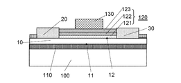
図8は前記第2領域と第3領域間の前記第1半導体薄膜にトランジスタ要素を組み込んだ場合の第3実施様態の断面図を示す。図8において、120は第1半導体薄膜10の第2表面12に接して設けられた第2絶縁膜、130は該第2絶縁膜に接して設けられた第2導電膜である。これらは少なくとも前記第2領域と第3領域の間の第1半導体薄膜上に設けられ、電界効果トランジスタのゲート絶縁膜、ゲートに対応するトランジスタ要素を構成している。前記第1半導体薄膜は該トランジスタ要素のチャネル構成領域としても機能する。
第2絶縁膜としては酸化アルミニウム、シリコン酸化膜、シリコン窒化膜、酸化ハフニウムなど高誘電率膜が用いられる。必要に応じて第1半導体薄膜との界面にバッファー層を設ける。
第2導電膜はアルミニウム、TiNなどが用いられる。
第2絶縁膜としては酸化アルミニウム、シリコン酸化膜、シリコン窒化膜、酸化ハフニウムなど高誘電率膜が用いられる。必要に応じて第1半導体薄膜との界面にバッファー層を設ける。
第2導電膜はアルミニウム、TiNなどが用いられる。
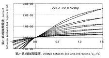
第5実施例として図8の第3実施様態の構成を有する第5実施例の半導体デバイスを試作した。第1導電性領域100、第1絶縁膜110、第1半導体薄膜、第2領域、第3領域の材料および厚さ方向の寸法は第1実施例と同じである。第2絶縁膜120は20nm厚の酸化アルミニウムとバッファー層、第2導電膜130は140nm厚のアルミニウム薄膜である。第2領域、第3領域間隔は10.5μm、第2領域20と第2導電膜130との距離は4.5μm、第3領域と第2導電膜との距離は4μm、第2導電膜の第2領域と第3領域を結ぶ方向の長さ(ゲート長に相当)は2μm、第2領域と第3領域を結ぶ方向に直角方向の長さ(ゲート幅に相当)は2.9mmである。
図9はこの第5実施例の半導体デバイスの電流電圧特性である。電流I23、電圧V23は第2領域、第3領域から取り出されているが、第2導電膜の電位V2が変化するにしたがって、電流が変化している。この電流変化は第2導電膜下のトランジスタ要素の特性が現れている。なお、第1導電性領域の電位V1は0V一定としている。
図9はこの第5実施例の半導体デバイスの電流電圧特性である。電流I23、電圧V23は第2領域、第3領域から取り出されているが、第2導電膜の電位V2が変化するにしたがって、電流が変化している。この電流変化は第2導電膜下のトランジスタ要素の特性が現れている。なお、第1導電性領域の電位V1は0V一定としている。
図10は図8の第2絶縁膜を第1層121、第2層122、第3層123と3層構造の第2多層膜120とした場合の第4実施様態を示し、第1半導体薄膜に接する第1層121をシリコン酸化膜、その上の第2層122をシリコン窒化膜、さらにその上の第3層を酸化アルミニウムとするなど記憶要素を第2領域、第3領域の間の第1半導体薄膜の上に作りこみ、記憶機能を有する半導体デバイスを実現することが出来る。なお、該第2多層膜は2層構造でも記憶機構を実現することは出来る。
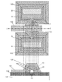
図11は本発明の第5実施様態を示す。図8記載の番号は図11でも同様な構成要素を示す。図11では1で示される矢印は第1半導体薄膜の延在する第1方向を示す。
第2表面12は、図11において点線の囲み13で示される部分で該第1方向を軸として前記第1半導体薄膜10の一部を囲む形状を有する。図11には2-2と記された二点鎖線で点線の囲み13で示される部分が切断された断面図も同時に示されている。その部分での前記第1半導体薄膜の第1方向と直交する断面の外周は外に凸の形状を有している。図11ではこの断面形状は台形であるが、該凸の形状は円形、楕円形、多角形等任意の閉図形の一部である。第2表面12は該点線の囲み13で示される部分で第1半導体薄膜をすべて囲んだ構造でもよい。図11の実施様態の場合は、「}14」で示されている台形の底面は第2表面が第1半導体薄膜を囲んでいないので「一部を囲む」と記述しているが、該点線の囲み部分13で第1半導体薄膜10を第1絶縁膜110、第1導電性領域100と離間させ、第2表面で第1半導体薄膜のすべてを囲む構造とすることも出来る。
第2表面12は、図11において点線の囲み13で示される部分で該第1方向を軸として前記第1半導体薄膜10の一部を囲む形状を有する。図11には2-2と記された二点鎖線で点線の囲み13で示される部分が切断された断面図も同時に示されている。その部分での前記第1半導体薄膜の第1方向と直交する断面の外周は外に凸の形状を有している。図11ではこの断面形状は台形であるが、該凸の形状は円形、楕円形、多角形等任意の閉図形の一部である。第2表面12は該点線の囲み13で示される部分で第1半導体薄膜をすべて囲んだ構造でもよい。図11の実施様態の場合は、「}14」で示されている台形の底面は第2表面が第1半導体薄膜を囲んでいないので「一部を囲む」と記述しているが、該点線の囲み部分13で第1半導体薄膜10を第1絶縁膜110、第1導電性領域100と離間させ、第2表面で第1半導体薄膜のすべてを囲む構造とすることも出来る。
上記断面の外周を第2導電膜130で囲む割合が大きいほど第1導電性領域の電位の影響を受けることなく、13部分の電流電圧特性はより第2導電膜の電位で制御されるようになり、半導体デバイスの設計が単純化される。すなわち、前記第2領域と第3領域間の前記第1半導体薄膜に組み込んだトランジスタ要素の設計と該トランジスタ要素の電流電圧特性を引き出す部分---該トランジスタ要素部分から第2領域、第3領域まで---の電流電圧特性とを独立して最適設計が可能となる。
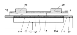
前記第1導電性領域への電位を支持基板から独立して与えるために前記第1導電性領域を絶縁性支持基板200上に設けた第6実施形態を図12に示す。図では該絶縁性支持基板200は導電性支持基板220上に絶縁膜210を設けて構成されている。
同様に前記第1導電性領域への電位を支持基板から独立して与えるために前記第1導電性領域を半導体基板230表面領域にpn接合103を形成して電気的に分離して設けた第7実施形態を図13に示す。この場合、前記第1導電性領域は該半導体基板230とは逆導電形の半導体であり、与えられる電位は接合103が逆バイアスされる極性の電位のみ可能である。
本発明の技術により、LSIの多層配線の上に低温でメモリブロックなど機能ブロックが搭載できるので、信号処理にフレキシビリティを与えることが出来、電子機器の高機能化が促進される。
また、本発明の低温技術により、ガラス基板、有機フレキシブル基板上のディスプレイ回路またはセンサ回路に制御、メモリ機能を搭載することが出来る。
また、本発明の低温技術により、ガラス基板、有機フレキシブル基板上のディスプレイ回路またはセンサ回路に制御、メモリ機能を搭載することが出来る。
1 第1方向を表す矢印
2←→2 上記第1方向と直交する方向で、第1半導体薄膜を切断する線
10 第1半導体薄膜
11 第1半導体薄膜の第1表面
12 第1半導体薄膜の第2表面
13 第1半導体薄膜の閉図形の一部の断面を有する部分
15 パッシベーション膜
20 第2領域
21 第2領域の一部
22 第2領域の一部
30 第3領域
31 第3領域の一部
32 第3領域の一部
100 第1導電性領域
101 第1導電性領域の第1表面
102 第1導電性領域の第2表面
103 第1導電性領域と半導体基板の接合
110 第1絶縁膜
120 第2絶縁膜
120 第2多層膜
121 第2多層膜の第1層
122 第2多層膜の第2層
123 第2多層膜の第3層
130 第2導電膜
200 絶縁性支持基板
201 導電性基板の第1表面
210 第3絶縁膜
220 導電性支持基板
230 半導体基板
2←→2 上記第1方向と直交する方向で、第1半導体薄膜を切断する線
10 第1半導体薄膜
11 第1半導体薄膜の第1表面
12 第1半導体薄膜の第2表面
13 第1半導体薄膜の閉図形の一部の断面を有する部分
15 パッシベーション膜
20 第2領域
21 第2領域の一部
22 第2領域の一部
30 第3領域
31 第3領域の一部
32 第3領域の一部
100 第1導電性領域
101 第1導電性領域の第1表面
102 第1導電性領域の第2表面
103 第1導電性領域と半導体基板の接合
110 第1絶縁膜
120 第2絶縁膜
120 第2多層膜
121 第2多層膜の第1層
122 第2多層膜の第2層
123 第2多層膜の第3層
130 第2導電膜
200 絶縁性支持基板
201 導電性基板の第1表面
210 第3絶縁膜
220 導電性支持基板
230 半導体基板
Claims (9)
- 第1導電性領域と、該第1導電性領域に接して設けられた第1絶縁膜と、第1表面と第2表面を有する第1半導体薄膜と、該第1半導体薄膜と異種材料の第2領域と、該第1半導体薄膜と異種材料の第3領域と、から少なくとも構成され、該第1半導体薄膜は該第1表面で該第1絶縁膜と接して設けられ、該第2領域と該第3領域は互いに離間して該第2表面で該第1半導体薄膜と接して設けられ、該第2表面と該第2領域が接する部分でまたは該第2表面と該第3領域が接する部分で該第2表面は該第1表面と対向し該第1表面と該第2表面間の該第1半導体薄膜に空間電荷層が形成されていることを特徴とする半導体デバイス。
- 請求項1記載の半導体デバイスにおいて、前記第2領域と前記第3領域間の前記第1半導体薄膜の前記第2表面に設けられた第2絶縁膜と、該第2絶縁膜に接して、かつ前記第2領域、前記第3領域と離間して設けられた第2導電膜とから、更に構成されたことを特徴とする請求項1記載の半導体デバイス。
- 前記第2表面と前記第2絶縁膜と前記第2導電膜は前記第1半導体薄膜の延在する第1方向を軸として前記第1半導体薄膜を前記第2領域と前記第3領域間で少なくとも一部囲む形状を有し、その部分での前記第1半導体薄膜の前記第1方向と直交する断面の外周は外に凸の形状を有することを特徴とする請求項2記載の半導体デバイス。
- 前記断面外周のうち前記第2絶縁膜に覆われない部分の幅が前記第1半導体薄膜の厚さの2倍以下であることを特徴とする請求項3記載の半導体デバイス。
- 前記第2絶縁膜を第2多層膜としたことを特徴とする請求項2記載の半導体デバイス。
- 前記第1導電性領域は半導体基板であることを特徴とする請求項1記載の半導体デバイス。
- 更に支持基板が設けられ、前記第1導電性領域は該支持基板上に電気的に分離されて設けられていることを特徴とする請求項1記載の半導体デバイス。
- 前記第2領域および前記第3領域はアルミニウム薄膜であることを特徴とする請求項1記載の半導体デバイス。
- 前記第2領域および前記第3領域は金属と水素化アモルファスシリコンの2層膜で、該水素化アモルファスシリコンが第1半導体薄膜に接していることを特徴とする請求項1記載の半導体デバイス。
Priority Applications (1)
| Application Number | Priority Date | Filing Date | Title |
|---|---|---|---|
| JP2015513616A JP6120340B2 (ja) | 2013-04-24 | 2014-03-18 | 異種材料接合を有する半導体デバイス |
Applications Claiming Priority (2)
| Application Number | Priority Date | Filing Date | Title |
|---|---|---|---|
| JP2013091373 | 2013-04-24 | ||
| JP2013-091373 | 2013-04-24 |
Publications (1)
| Publication Number | Publication Date |
|---|---|
| WO2014174937A1 true WO2014174937A1 (ja) | 2014-10-30 |
Family
ID=51791522
Family Applications (1)
| Application Number | Title | Priority Date | Filing Date |
|---|---|---|---|
| PCT/JP2014/057314 Ceased WO2014174937A1 (ja) | 2013-04-24 | 2014-03-18 | 異種材料接合を有する半導体デバイス |
Country Status (2)
| Country | Link |
|---|---|
| JP (1) | JP6120340B2 (ja) |
| WO (1) | WO2014174937A1 (ja) |
Cited By (3)
| Publication number | Priority date | Publication date | Assignee | Title |
|---|---|---|---|---|
| CN106298961A (zh) * | 2016-11-11 | 2017-01-04 | 河南大学 | 薄膜晶体管及其制备方法 |
| CN107425057A (zh) * | 2016-04-04 | 2017-12-01 | 格罗方德半导体公司 | 包括在衬底中设有栅极电极区的晶体管的半导体结构及其形成方法 |
| CN109256419A (zh) * | 2017-07-12 | 2019-01-22 | 格芯公司 | 利用埋置绝缘层作为栅极介电质的高压晶体管 |
Citations (5)
| Publication number | Priority date | Publication date | Assignee | Title |
|---|---|---|---|---|
| JP2007287859A (ja) * | 2006-04-14 | 2007-11-01 | Toshiba Corp | 半導体装置の製造方法 |
| JP2009016756A (ja) * | 2007-07-09 | 2009-01-22 | Nec Lcd Technologies Ltd | アクティブマトリクス駆動表示装置 |
| JP2009530820A (ja) * | 2006-03-16 | 2009-08-27 | マイクロン テクノロジー, インク. | 炭化ケイ素ベースのアモルファスシリコン薄膜トランジスタを有するスタック不揮発性メモリとその製造方法 |
| JP2013051425A (ja) * | 2006-03-31 | 2013-03-14 | Semiconductor Energy Lab Co Ltd | 半導体装置 |
| JP2013055348A (ja) * | 2012-11-12 | 2013-03-21 | Semiconductor Energy Lab Co Ltd | 半導体装置 |
Family Cites Families (7)
| Publication number | Priority date | Publication date | Assignee | Title |
|---|---|---|---|---|
| RU2130668C1 (ru) * | 1994-09-30 | 1999-05-20 | Акционерное общество закрытого типа "VL" | Полевой транзистор типа металл - диэлектрик-полупроводник |
| JPH1187718A (ja) * | 1997-09-05 | 1999-03-30 | Denso Corp | 半導体装置 |
| JP4704629B2 (ja) * | 2001-09-07 | 2011-06-15 | 株式会社リコー | 薄膜トランジスタ及びその製造方法 |
| JP2003188383A (ja) * | 2001-12-14 | 2003-07-04 | Hitachi Ltd | 半導体集積回路装置及びその製造方法 |
| DE102005039365B4 (de) * | 2005-08-19 | 2022-02-10 | Infineon Technologies Ag | Gate-gesteuertes Fin-Widerstandselement, welches als pinch - resistor arbeitet, zur Verwendung als ESD-Schutzelement in einem elektrischen Schaltkreis und Einrichtung zum Schutz vor elektrostatischen Entladungen in einem elektrischen Schaltkreis |
| CN102668028B (zh) * | 2009-11-28 | 2015-09-02 | 株式会社半导体能源研究所 | 层叠的氧化物材料、半导体器件、以及用于制造该半导体器件的方法 |
| JP5740643B2 (ja) * | 2010-09-22 | 2015-06-24 | 国立研究開発法人産業技術総合研究所 | 電界効果トランジスタ |
-
2014
- 2014-03-18 WO PCT/JP2014/057314 patent/WO2014174937A1/ja not_active Ceased
- 2014-03-18 JP JP2015513616A patent/JP6120340B2/ja active Active
Patent Citations (5)
| Publication number | Priority date | Publication date | Assignee | Title |
|---|---|---|---|---|
| JP2009530820A (ja) * | 2006-03-16 | 2009-08-27 | マイクロン テクノロジー, インク. | 炭化ケイ素ベースのアモルファスシリコン薄膜トランジスタを有するスタック不揮発性メモリとその製造方法 |
| JP2013051425A (ja) * | 2006-03-31 | 2013-03-14 | Semiconductor Energy Lab Co Ltd | 半導体装置 |
| JP2007287859A (ja) * | 2006-04-14 | 2007-11-01 | Toshiba Corp | 半導体装置の製造方法 |
| JP2009016756A (ja) * | 2007-07-09 | 2009-01-22 | Nec Lcd Technologies Ltd | アクティブマトリクス駆動表示装置 |
| JP2013055348A (ja) * | 2012-11-12 | 2013-03-21 | Semiconductor Energy Lab Co Ltd | 半導体装置 |
Cited By (3)
| Publication number | Priority date | Publication date | Assignee | Title |
|---|---|---|---|---|
| CN107425057A (zh) * | 2016-04-04 | 2017-12-01 | 格罗方德半导体公司 | 包括在衬底中设有栅极电极区的晶体管的半导体结构及其形成方法 |
| CN106298961A (zh) * | 2016-11-11 | 2017-01-04 | 河南大学 | 薄膜晶体管及其制备方法 |
| CN109256419A (zh) * | 2017-07-12 | 2019-01-22 | 格芯公司 | 利用埋置绝缘层作为栅极介电质的高压晶体管 |
Also Published As
| Publication number | Publication date |
|---|---|
| JPWO2014174937A1 (ja) | 2017-02-23 |
| JP6120340B2 (ja) | 2017-04-26 |
Similar Documents
| Publication | Publication Date | Title |
|---|---|---|
| JP5536328B2 (ja) | トランジスタ及びその製造方法 | |
| US10971621B2 (en) | Semiconductor device | |
| CN102136499B (zh) | 薄膜晶体管及其制造方法 | |
| KR20130032105A (ko) | 그래핀을 포함하는 전극 구조체 및 전계효과 트랜지스터 | |
| KR102618541B1 (ko) | 이차원 물질층을 포함하는 전자 소자 | |
| KR102525247B1 (ko) | 전기적 접속 구조, 반도체 장치 및 전자 기기 | |
| US20160064550A1 (en) | Insulated gate type switching device | |
| KR101966531B1 (ko) | 터널링 전계효과 트랜지스터 | |
| KR20120112647A (ko) | 전계 효과 트랜지스터 및 반도체 장치 | |
| KR102257243B1 (ko) | 튜너블 배리어를 구비한 그래핀 트랜지스터 | |
| JP2016072498A (ja) | 半導体装置 | |
| JPWO2019107411A1 (ja) | トンネル電界効果トランジスタおよび電子デバイス | |
| WO2011142073A1 (ja) | 薄膜トランジスタ装置及びその製造方法 | |
| KR101587129B1 (ko) | 양방향성 트랜지스터 및 그 제조방법 | |
| Jeon et al. | Contact properties of a low-resistance aluminum-based electrode with metal capping layers in vertical oxide thin-film transistors | |
| JP6120340B2 (ja) | 異種材料接合を有する半導体デバイス | |
| KR102118531B1 (ko) | 반도체 디바이스 및 그 제조 방법 | |
| KR101069331B1 (ko) | 반도체 소자 평가 방법 | |
| KR20150087060A (ko) | 접착층을 포함하는 전극 연결 구조체 및 이를 포함하는 전자 소자 | |
| CN102017161B (zh) | 半导体装置 | |
| KR102192083B1 (ko) | 높은 온/오프 전류비를 가진 박막 트랜지스터 | |
| KR20230030347A (ko) | 2차원 물질을 포함하는 전자 소자 및 그 제조 방법 | |
| KR102634054B1 (ko) | 일렉트라이드 전극을 포함하는 트랜지스터 | |
| CN102891185B (zh) | 半导体结构及其制造方法 | |
| JP2016072499A (ja) | 半導体装置 |
Legal Events
| Date | Code | Title | Description |
|---|---|---|---|
| 121 | Ep: the epo has been informed by wipo that ep was designated in this application |
Ref document number: 14788848 Country of ref document: EP Kind code of ref document: A1 |
|
| ENP | Entry into the national phase |
Ref document number: 2015513616 Country of ref document: JP Kind code of ref document: A |
|
| NENP | Non-entry into the national phase |
Ref country code: DE |
|
| 122 | Ep: pct application non-entry in european phase |
Ref document number: 14788848 Country of ref document: EP Kind code of ref document: A1 |