WO2014157841A1 - 투명 전극 패턴 적층체 및 이를 구비한 터치 스크린 패널 - Google Patents
투명 전극 패턴 적층체 및 이를 구비한 터치 스크린 패널 Download PDFInfo
- Publication number
- WO2014157841A1 WO2014157841A1 PCT/KR2014/001408 KR2014001408W WO2014157841A1 WO 2014157841 A1 WO2014157841 A1 WO 2014157841A1 KR 2014001408 W KR2014001408 W KR 2014001408W WO 2014157841 A1 WO2014157841 A1 WO 2014157841A1
- Authority
- WO
- WIPO (PCT)
- Prior art keywords
- transparent electrode
- layer
- transparent
- electrode layer
- laminate
- Prior art date
- Legal status (The legal status is an assumption and is not a legal conclusion. Google has not performed a legal analysis and makes no representation as to the accuracy of the status listed.)
- Ceased
Links
Images


Classifications
-
- G—PHYSICS
- G06—COMPUTING OR CALCULATING; COUNTING
- G06F—ELECTRIC DIGITAL DATA PROCESSING
- G06F3/00—Input arrangements for transferring data to be processed into a form capable of being handled by the computer; Output arrangements for transferring data from processing unit to output unit, e.g. interface arrangements
- G06F3/01—Input arrangements or combined input and output arrangements for interaction between user and computer
- G06F3/03—Arrangements for converting the position or the displacement of a member into a coded form
- G06F3/041—Digitisers, e.g. for touch screens or touch pads, characterised by the transducing means
- G06F3/044—Digitisers, e.g. for touch screens or touch pads, characterised by the transducing means by capacitive means
- G06F3/0443—Digitisers, e.g. for touch screens or touch pads, characterised by the transducing means by capacitive means using a single layer of sensing electrodes
-
- G—PHYSICS
- G06—COMPUTING OR CALCULATING; COUNTING
- G06F—ELECTRIC DIGITAL DATA PROCESSING
- G06F3/00—Input arrangements for transferring data to be processed into a form capable of being handled by the computer; Output arrangements for transferring data from processing unit to output unit, e.g. interface arrangements
- G06F3/01—Input arrangements or combined input and output arrangements for interaction between user and computer
- G06F3/03—Arrangements for converting the position or the displacement of a member into a coded form
- G06F3/041—Digitisers, e.g. for touch screens or touch pads, characterised by the transducing means
-
- G—PHYSICS
- G06—COMPUTING OR CALCULATING; COUNTING
- G06F—ELECTRIC DIGITAL DATA PROCESSING
- G06F3/00—Input arrangements for transferring data to be processed into a form capable of being handled by the computer; Output arrangements for transferring data from processing unit to output unit, e.g. interface arrangements
- G06F3/01—Input arrangements or combined input and output arrangements for interaction between user and computer
- G06F3/03—Arrangements for converting the position or the displacement of a member into a coded form
- G06F3/033—Pointing devices displaced or positioned by the user, e.g. mice, trackballs, pens or joysticks; Accessories therefor
- G06F3/0354—Pointing devices displaced or positioned by the user, e.g. mice, trackballs, pens or joysticks; Accessories therefor with detection of two-dimensional [2D] relative movements between the device, or an operating part thereof, and a plane or surface, e.g. 2D mice, trackballs, pens or pucks
- G06F3/03545—Pens or stylus
-
- G—PHYSICS
- G06—COMPUTING OR CALCULATING; COUNTING
- G06F—ELECTRIC DIGITAL DATA PROCESSING
- G06F3/00—Input arrangements for transferring data to be processed into a form capable of being handled by the computer; Output arrangements for transferring data from processing unit to output unit, e.g. interface arrangements
- G06F3/01—Input arrangements or combined input and output arrangements for interaction between user and computer
- G06F3/03—Arrangements for converting the position or the displacement of a member into a coded form
- G06F3/041—Digitisers, e.g. for touch screens or touch pads, characterised by the transducing means
- G06F3/044—Digitisers, e.g. for touch screens or touch pads, characterised by the transducing means by capacitive means
- G06F3/0446—Digitisers, e.g. for touch screens or touch pads, characterised by the transducing means by capacitive means using a grid-like structure of electrodes in at least two directions, e.g. using row and column electrodes
-
- G—PHYSICS
- G06—COMPUTING OR CALCULATING; COUNTING
- G06F—ELECTRIC DIGITAL DATA PROCESSING
- G06F3/00—Input arrangements for transferring data to be processed into a form capable of being handled by the computer; Output arrangements for transferring data from processing unit to output unit, e.g. interface arrangements
- G06F3/01—Input arrangements or combined input and output arrangements for interaction between user and computer
- G06F3/048—Interaction techniques based on graphical user interfaces [GUI]
- G06F3/0487—Interaction techniques based on graphical user interfaces [GUI] using specific features provided by the input device, e.g. functions controlled by the rotation of a mouse with dual sensing arrangements, or of the nature of the input device, e.g. tap gestures based on pressure sensed by a digitiser
- G06F3/0488—Interaction techniques based on graphical user interfaces [GUI] using specific features provided by the input device, e.g. functions controlled by the rotation of a mouse with dual sensing arrangements, or of the nature of the input device, e.g. tap gestures based on pressure sensed by a digitiser using a touch-screen or digitiser, e.g. input of commands through traced gestures
-
- H—ELECTRICITY
- H01—ELECTRIC ELEMENTS
- H01B—CABLES; CONDUCTORS; INSULATORS; SELECTION OF MATERIALS FOR THEIR CONDUCTIVE, INSULATING OR DIELECTRIC PROPERTIES
- H01B5/00—Non-insulated conductors or conductive bodies characterised by their form
- H01B5/14—Non-insulated conductors or conductive bodies characterised by their form comprising conductive layers or films on insulating-supports
-
- B—PERFORMING OPERATIONS; TRANSPORTING
- B32—LAYERED PRODUCTS
- B32B—LAYERED PRODUCTS, i.e. PRODUCTS BUILT-UP OF STRATA OF FLAT OR NON-FLAT, e.g. CELLULAR OR HONEYCOMB, FORM
- B32B2459/00—Nets, e.g. camouflage nets
-
- G—PHYSICS
- G06—COMPUTING OR CALCULATING; COUNTING
- G06F—ELECTRIC DIGITAL DATA PROCESSING
- G06F2203/00—Indexing scheme relating to G06F3/00 - G06F3/048
- G06F2203/041—Indexing scheme relating to G06F3/041 - G06F3/045
- G06F2203/04103—Manufacturing, i.e. details related to manufacturing processes specially suited for touch sensitive devices
-
- G—PHYSICS
- G06—COMPUTING OR CALCULATING; COUNTING
- G06F—ELECTRIC DIGITAL DATA PROCESSING
- G06F2203/00—Indexing scheme relating to G06F3/00 - G06F3/048
- G06F2203/041—Indexing scheme relating to G06F3/041 - G06F3/045
- G06F2203/04111—Cross over in capacitive digitiser, i.e. details of structures for connecting electrodes of the sensing pattern where the connections cross each other, e.g. bridge structures comprising an insulating layer, or vias through substrate
-
- G—PHYSICS
- G06—COMPUTING OR CALCULATING; COUNTING
- G06F—ELECTRIC DIGITAL DATA PROCESSING
- G06F2203/00—Indexing scheme relating to G06F3/00 - G06F3/048
- G06F2203/048—Indexing scheme relating to G06F3/048
- G06F2203/04804—Transparency, e.g. transparent or translucent windows
-
- G—PHYSICS
- G06—COMPUTING OR CALCULATING; COUNTING
- G06F—ELECTRIC DIGITAL DATA PROCESSING
- G06F3/00—Input arrangements for transferring data to be processed into a form capable of being handled by the computer; Output arrangements for transferring data from processing unit to output unit, e.g. interface arrangements
- G06F3/01—Input arrangements or combined input and output arrangements for interaction between user and computer
- G06F3/03—Arrangements for converting the position or the displacement of a member into a coded form
- G06F3/041—Digitisers, e.g. for touch screens or touch pads, characterised by the transducing means
- G06F3/0412—Digitisers structurally integrated in a display
Definitions
- the present invention relates to a transparent electrode laminate and a touch screen panel having the same, and more particularly, to a transparent electrode laminate having low visibility to a user and a touch screen panel having the same.
- a touch screen panel is a screen panel equipped with a special input device that receives a position when touched by hand.
- the touch screen panel receives input data directly from the screen so that when a person's hand or an object touches a character or a specific location displayed on the screen without using a keyboard, the touch screen panel can identify the location and perform specific processing by the stored software. It is made possible by being laminated
- the use of the transparent electrode is essential, and typically, a transparent electrode formed in a predetermined pattern is used.
- GFF glass-ITO film-ITO film
- G1F glass-ITO film
- G2 glass-only
- GFF is the most common structure, and the transparent electrode (ITO) required to implement the X and Y axes is composed of two films.
- G1F is a thin film of ITO deposited on the back of the glass, and the second ITO is a film like the conventional method.
- Use G2 is a method of forming a thin film by depositing and patterning the X-axis ITO on the back side using one sheet of tempered glass, and then patterning and forming the Y-axis ITO even after forming an insulating layer thereon.
- the pattern portion and the non-pattern portion (pattern opening) of the transparent electrode can be visually distinguished, and as the difference in reflectance between the pattern portion and the non-pattern portion increases, the difference is increased. Since it becomes clear, there exists a problem that the visibility of the external appearance as a display element falls. In particular, in the capacitive touch panel, since the patterned transparent electrode layer is formed on the entire surface of the display display portion, even when the transparent electrode layer is patterned, a good appearance is required as the display element.
- JP-A-2008-98169 of Patent Document 1 discloses a transparent conductive film in which an undercoat layer composed of two layers having different refractive indices is formed between a transparent substrate and a transparent conductive layer. Is proposed.
- a silicon tin oxide layer (thickness of 10 nm or more) having a refractive index of 1.7 as a high refractive index layer on a transparent substrate, a silicon oxide layer having a refractive index of 1.43 as a low refractive index layer (thickness of 30 nm), and an ITO film having a refractive index of 1.95 as a transparent conductive layer
- the transparent conductive film which formed (thickness 15nm) in this order is described.
- Patent Document 1 Japanese Unexamined Patent Publication No. 2008-98169
- An object of the present invention is to provide a transparent electrode laminate having little visibility difference in reflectance for each position of a pattern.
- an object of this invention is to provide the transparent electrode laminated body which does not have a transparent dielectric layer between a transparent substrate and a transparent electrode layer.
- an object of this invention is to provide the touch screen panel provided with the said transparent electrode laminated body.
- a first transparent electrode layer and a second transparent electrode layer each insulating layer interposed between the first transparent electrode layer and the second transparent electrode layer, stacked in a predetermined pattern on a transparent substrate, respectively, formed on the insulating layer and the first transparent
- a contact hole electrically connecting the electrode layer and the second transparent electrode layer, wherein each of the first transparent electrode layer and the second transparent electrode layer has a thickness of 100 to 200 nm, and the insulating layer has a thickness of 1,000 to 2,000 nm.
- the transparent electrode laminate according to claim 1 further comprising a passivation layer on an opposite side of the transparent substrate with respect to the transparent electrode laminate.
- transparent electrode laminate of 1 above wherein the transparent substrate further comprises at least one optical function layer on a surface opposite to the surface on which the transparent electrode is formed.
- optical functional layer is at least one layer of the anti-reflection layer and the anti-fouling layer transparent electrode laminate.
- Touch screen panel provided with the transparent electrode laminated body of any one of Claims 1-10.
- the transparent electrode laminate of the present invention adjusts the thickness of each layer constituting the laminate to a specific range, thereby minimizing the difference in reflectance by position caused by the patterned transparent electrode structure, thereby reducing the visibility to the user. Transparency is shown.
- the transparent electrode laminate of the present invention can be very usefully used by showing high transmittance and low reflectance when applied to a touch screen panel having a G2 structure.
- the transparent electrode laminate of the present invention can exhibit low visibility even without providing a transparent dielectric layer between the substrate and the transparent electrode layer.
- FIG. 1 is a schematic plan view of one embodiment of a transparent electrode laminate of the present invention.
- FIG. 2 is a schematic plan view of a unit structure in one embodiment of the transparent electrode stack of the present invention.
- FIG. 3 is a schematic cross-sectional view showing the laminated structure of each position of the transparent electrode laminate of the present invention.
- the present invention includes a first transparent electrode layer and a second transparent electrode layer, each insulating layer interposed between the first transparent electrode layer and the second transparent electrode layer stacked in a predetermined pattern on the transparent substrate, the insulating layer is formed on the first And a contact hole electrically connecting the transparent electrode layer and the second transparent electrode layer, wherein each of the first transparent electrode layer and the second transparent electrode layer has a thickness of 20 to 200 nm, and the insulating layer has a thickness of 1,000 to 2,000 nm.
- the present invention relates to a transparent electrode pattern laminate and a touch screen panel having the same, which can remarkably reduce a difference in reflectance at each position.
- FIG. 1 is a schematic plan view of one embodiment of a transparent electrode laminate of the present invention.
- the transparent electrode laminate of the present invention may include a first transparent electrode layer 100, a second transparent electrode layer 200, an insulating layer 300, and a contact hole 400.
- the transparent electrode laminate of the present invention may be formed on a transparent substrate (not shown), the passivation layer (not shown) may be further provided on the opposite side of the transparent substrate.
- the transparent electrode laminate is formed in a predetermined pattern.
- the first transparent electrode layer 100 and the second transparent electrode layer 200 provide position information of a touched point, and the insulating layer 300 is disposed between the first transparent electrode layer 100 and the second transparent electrode layer 200.
- the two layers are electrically separated from each other, and the contact hole 400 is formed in the insulating layer 300 so that the first transparent electrode layer 100 and the second transparent electrode layer 200 can be electrically connected to each other.
- each structure of the transparent electrode laminate is formed in a predetermined pattern, and according to the pattern structure, the transparent electrode laminate has a different laminate structure depending on its position.
- the transparent electrode laminate may have five types of stacked structures from 1 to 5 depending on the position. 3 schematically shows the lamination structure in the above 1 to 5 positions.
- the transparent electrode laminate has various layer structures. Due to the various layer structures according to the positions, differences in reflectance, luminance, color difference, etc. occur for each position, and accordingly, visibility of the pattern is increased, thereby making it transparent. There is a limit to the function as an electrode.
- the present invention solves the above problems by minimizing the difference in reflectance by having a specific thickness range of the transparent electrode layer and the insulating layer.
- the present invention will be described in more detail.
- the present invention includes a first transparent electrode layer and a second transparent electrode layer.
- the first transparent electrode layer 100 may be formed of the first pattern 110 and the second pattern 120.
- the first pattern 110 and the second pattern 120 are disposed in the same row or column direction, respectively, to provide information about the X and Y coordinates of the touched point.
- the first circuit 110, the second pattern 120, the second transparent electrode layer 200, and the position detection line via the position detection line toward the contact position The change in capacitance is thus conveyed.
- the contact position is grasped by the change of the capacitance converted into an electrical signal by the X and Y input processing circuit (not shown) or the like.
- the first pattern 110 and the second pattern 120 are formed on the same layer (first transparent electrode layer), and the respective patterns must be electrically connected to detect a touched point.
- the first pattern 110 is connected to each other but the second pattern 120 has an island-like structure, a separate connection line is required to electrically connect the second pattern 120. .
- connection line should not be electrically connected to the first pattern 110, the connection line should be formed on a layer different from the first transparent electrode layer 100. Accordingly, the second transparent electrode layer 200 is formed on a separate layer different from the first transparent electrode layer 100 to electrically connect the second pattern 120. That is, the second transparent electrode layer 200 functions to electrically connect the second pattern 120 of the first transparent electrode layer 100.
- the positions 1, 3, and 4 are portions in which the first transparent electrode layer 100 is formed in a predetermined pattern to detect a touched portion, and the positions 3, 4, and 5 are formed in an island shape.
- the second transparent electrode layer 200 formed to electrically connect the two patterns 120 is present.
- the second transparent electrode layer 200 since the second transparent electrode layer 200 must be electrically blocked from the first pattern 110 of the first transparent electrode layer 100, for this purpose, the insulating layer 300 and the contact hole 400 (3 in FIG. 2). ) Is provided, which will be described later.
- each of the first transparent electrode layer 100 and the second transparent electrode layer 200 has a thickness of 100 to 200 nm, respectively. If the thickness is out of the above range, there is a problem in that the reflectance difference of each position is increased to increase the reflection visibility of the pattern. Specifically, when the thickness is less than 100 nm, the electrical resistance becomes large, and the touch sensitivity is lowered. When the thickness is larger than 200 nm, the reflectance becomes large and a visibility problem occurs.
- the transparent electrode layer according to the present invention in the thickness of the above range, on the transparent substrate without the need for a transparent dielectric layer conventionally formed of a metal oxide (silicon oxide, niobium oxide, etc.) between the transparent substrate and the transparent electrode layer for optical uniformity. Even having a structure formed directly in contact with the substrate may exhibit low visibility similar to the case where a transparent dielectric layer is present.
- a transparent dielectric layer conventionally formed of a metal oxide (silicon oxide, niobium oxide, etc.) between the transparent substrate and the transparent electrode layer for optical uniformity.
- first transparent electrode layer 100 and the second transparent electrode layer 200 preferably have a refractive index of 1.8 to 1.98, respectively.
- the reflectance reduction effect in the case of having the above-mentioned thickness range in the refractive index range can be further enhanced.
- the first transparent electrode layer 100 and the second transparent electrode layer 200 according to the present invention may be applied without limitation to the transparent electrode material known in the art.
- indium tin oxide (ITO), indium zinc oxide (IZO), zinc oxide (ZnO), indium zinc oxide (IZTO), cadmium tin oxide (CTO), PEDOT (poly (3,4-ethylenedioxythiophene)) , Carbon nanotubes (CNT), metal wires, and the like and these may be used alone or in combination of two or more thereof.
- ITO indium tin oxide
- the metal used for a metal wire is not specifically limited, For example, silver (Ag), gold, aluminum, copper, iron, nickel, titanium, telenium, chromium, etc. are mentioned. These can be used individually or in mixture of 2 or more types.
- the transparent electrode layers 100 and 200 may be formed by various thin film deposition techniques such as physical vapor deposition (PVD) and chemical vapor deposition (CVD). For example, it may be formed by reactive sputtering, which is an example of physical vapor deposition.
- PVD physical vapor deposition
- CVD chemical vapor deposition
- the transparent electrode layers 100 and 200 may be formed by a printing process. In this printing process, various printing methods such as gravure off set, reverse off set, screen printing, and gravure printing may be used.
- the transparent electrode layers 100 and 200 may be formed of a printable paste material. For example, it may be formed of carbon nanotubes (CNTs), conductive polymers, and silver nano wire inks.
- the stacking order of the first transparent electrode layer 100 and the second transparent electrode layer 200 is not limited. Therefore, in another embodiment of the present invention, the stacking order of the first transparent electrode layer 100 and the second transparent electrode layer 200 of FIG. 3 may be changed. For example, a second transparent electrode layer may be first formed on the transparent substrate instead of the first transparent electrode layer, an insulating layer may be formed thereon, and then the first transparent electrode layer may be formed on the insulating layer.
- the insulating layer 300 is formed between the first transparent electrode layer 100 and the second transparent electrode layer 200 to prevent electrical connection between the first transparent electrode layer 100 and the second transparent electrode layer 200. 2 and 3, when the second transparent electrode layer 200 electrically connects the second pattern 120 of the adjacent first transparent electrode layer 100, the first transparent electrode layer 100 is used. Since it is to be electrically connected to the, it is necessary that a portion where the insulating layer 300 is not formed. As such, the portion of the insulating layer 300 where the insulating layer 300 is not formed is called the insulating layer 300 in the contact hole 400 (3 in FIG. 2). Therefore, the contact hole 400 makes electrical connection between the first transparent electrode layer (second pattern) and the second transparent electrode layer.
- the insulating layer 300 has a thickness of 1,000 to 2,000 nm. If the thickness is out of the above range, there is a problem in that the reflectance difference of each position is increased to increase the reflection visibility of the pattern. If the thickness is less than 1,000 nm, the capacitance value formed between the transparent electrodes becomes large, and the touch sensitivity is lowered. If the thickness is more than 2,000 nm, the effect of further thickness improvement does not appear.
- the insulating layer 300 preferably has a refractive index of 1.4 to 1.6.
- the reflectance reduction effect in the case of having the above-mentioned thickness range in the refractive index range can be further enhanced.
- the insulating layer 300 according to the present invention may be applied without limitation the transparent insulating material known in the art.
- it may be formed in a required pattern using a transparent photosensitive resin composition or a thermosetting resin composition containing a metal oxide such as silicon oxide or an acrylic resin.
- the insulating layer 300 may be formed on the first transparent electrode layer 100 by deposition or printing.
- the contact hole 400 may be formed by forming a hole after forming the insulating layer as a whole (hole method), and the insulating layer is electrically connected to the first transparent electrode layer and the second transparent electrode layer. It may also be formed in such a way as to form a part except for the part connected to the island (island method).
- the transparent substrate forms the outermost surface of the touch screen panel and is a part to which a human hand or an object directly contacts.
- the transparent electrode stack of the present invention is formed on the opposite side to which a human hand or an object directly comes into contact.
- the transparent electrode laminate of the present invention is formed by sequentially stacking a first transparent electrode layer on a transparent substrate.
- the transparent substrate is not particularly limited as long as it is durable to sufficiently protect the touch screen panel from external force, and a user can see the display well, and materials used in the art may be used without particular limitation.
- materials used in the art may be used without particular limitation.
- glass polyethersulphone (PES), polyacrylate (PAR, polyacrylate), polyetherimide (PEI), polyethylene naphthalate (PEN, polyethyelenen napthalate), polyethylene terephthalate (PET, polyethyelene terepthalate, polyphenylene sulfide (PPS), polyallylate, polyimide, polycarbonate (PC, polycarbonate), cellulose tri acetate (TAC), cellulose acetate propionate (cellulose acetate propionate (CAP) and the like may be used, preferably glass may be used, and more preferably tempered glass may be used.
- PES polyethersulphone
- PAR polyacrylate
- PEI polyetherimide
- PEN polyethylene naphthal
- the transparent substrate according to the present invention may have a suitable thickness, for example, may be 0.1 to 0.7mm. Within this range, the effect of reducing the reflectance of the transparent electrode laminate according to the present invention can be further improved.
- the transparent substrate preferably has a refractive index of 1.4 to 1.6.
- the reflectance reduction effect in the case of having the above-mentioned thickness range in the refractive index range can be further enhanced.
- the transparent substrate may further include at least one optical function layer on the surface opposite to the surface on which the transparent electrode is formed, if necessary.
- an optical function layer may be formed by a single antifouling layer such as an antireflection layer, a fingerprint antifouling layer, or the like, alone or in combination of two or more thereof.
- the transparent electrode laminate of the present invention if necessary, in order to prevent the transparent electrode layers 100 and 200 from being contaminated by an external environment (moisture, air, etc.), the surface on which the transparent substrate is bonded based on the transparent electrode laminate
- the passivation layer may be further provided on the opposite side of the substrate.
- the passivation layer may be formed by adopting a material usable in the insulating layer 300.
- the passivation layer according to the present invention may have a suitable thickness, for example, may be 2,000 nm or less. Thus, for example, it may be 0 to 2,000 nm. Within this range, the effect of reducing the reflectance of the transparent electrode laminate according to the present invention can be further improved.
- the passivation layer preferably has a refractive index of 1.4 to 1.6.
- the reflectance reduction effect in the case of having the above-mentioned thickness range in the refractive index range can be further enhanced.
- the adhesive layer bonds the transparent electrode laminated body of this invention with a display panel part.
- the adhesive layer may be formed by coating and curing the transparent curable resin composition (OCR), or may be formed by compressing an already cured film (OCA).
- the adhesive layer may also affect the reflectance of the transparent electrode laminate, and therefore, it is desirable to have a suitable thickness and refractive index for reducing the reflectance of the transparent electrode laminate.
- the thickness may be 0 to 250 ⁇ m and the refractive index may be 1 to 1.6. In the case where the thickness is 0 ⁇ m, when the adhesive layer is formed only at the edge of the transparent electrode stack, this means that the adhesive layer is not formed at the inner portion where the actual image is displayed. Only the air layer is present between the display panel units.
- the transparent electrode layer and the insulating layer may have a specific thickness range, thereby minimizing the difference in reflectance according to the position, and thus, the transparency may be significantly improved. Therefore, the transparent electrode laminate of the present invention may be manufactured as a touch screen panel having excellent transparency when bonded to the display panel unit.
- the transparent electrode laminated body was produced by the thickness of following Table 1, the average reflectance by each position was measured, and the difference of the maximum value and minimum value of the said average reflectance was described.
- the average reflectance means the average of the reflectance at 400nm ⁇ 700nm.
- ITO refractive index: 1.8, extinction coefficient: 0
- ITO reffractive index: 1.8, extinction coefficient: 0
- NCS-801 Silicon dioxide (Sumitomo Co., Ltd.) (refractive index: 1.51, extinction coefficient: 0), which is an acrylic insulating material, was used.
- the refractive index and the extinction coefficient were described based on light having a wavelength of 550 nm.
- the adhesive layer is described as air, it means that only the bezel part is bonded so that the image display area is not formed of the adhesive layer.
- Example 1 a transparent laminate manufactured in the same manner as in Example 3 was used except that a transparent dielectric layer formed of Nb 2 O 5 8 nm and SiO 2 50 nm was further provided between the transparent substrate and the first transparent electrode layer. It was.
- the transparent electrode laminate was manufactured with the thickness shown in Table 2 below, and the difference between the average reflectance at each position and the maximum and minimum values of the average reflectance was described.
- the average reflectance means the average of the reflectance at 400nm ⁇ 700nm.
- ITO refractive index: 1.8, extinction coefficient: 0.014
- ITO reffractive index: 1.8, extinction coefficient: 0.014
- NCS-801 Silicon dioxide (Sumitomo Co., Ltd.) (refractive index: 1.51, extinction coefficient: 0), which is an acrylic insulating material, was used.
- the refractive index and the extinction coefficient were described based on light having a wavelength of 550 nm.
- the adhesive layer is described as air, it means that only the bezel part is bonded so that the image display area is not formed of the adhesive layer.
- Example 2 a transparent laminate manufactured in the same manner as in Example 6 was used except that a transparent dielectric layer formed of Nb 2 O 5 8 nm and SiO 2 50 nm was further provided between the transparent substrate and the first transparent electrode layer. It was.
- the transparent electrode laminate was manufactured with the thickness shown in Table 3 below, and the difference between the average reflectance at each position and the maximum and minimum values of the average reflectance was described.
- the average reflectance means the average of the reflectance at 400nm ⁇ 700nm.
- ITO refractive index: 1.975, extinction coefficient: 0
- ITO refractive index: 1.975, extinction coefficient: 0.014
- NCS-801 Silicon dioxide (Sumitomo Co., Ltd.) (refractive index: 1.51, extinction coefficient: 0), which is an acrylic insulating material, was used.
- the refractive index and the extinction coefficient were described based on light having a wavelength of 550 nm.
- the adhesive layer is described as air, it means that only the bezel part is bonded so that the image display area is not formed of the adhesive layer.
- Example 3 a transparent laminate manufactured in the same manner as in Example 13 was used except that a transparent dielectric layer formed of Nb 2 O 5 8 nm and SiO 2 50 nm was further provided between the transparent substrate and the first transparent electrode layer. It was.
- the average reflectance is less than 13%, the reflectance itself is not high, and the difference between the reflectivity of each position is less than 4% between the maximum value and the minimum value of the average reflectance. It is not big so visibility is very low. In particular, even when compared to the reference examples in which the transparent dielectric layer is inserted for optical uniformity, the average reflectance difference of the embodiments not including the transparent dielectric layer may be confirmed to be similar to the reference examples.
- the average reflectance is sometimes higher than 13%, especially when the difference between the maximum value and the minimum value of the average reflectance is more than 4%, the visibility of each position is large and the visibility is very high. It was not suitable for use as a transparent electrode.
- Comparative Examples 1, 4, 5, 7, 9, and 10 the average reflectance difference was 4% or less, but the comparative examples are cases in which the thicknesses of the first transparent electrode layer and the second transparent electrode layer were 50 nm or less. When the thickness of the transparent electrode layer was 50 nm or less, the electrical conductivity was lowered, and the basic function as the electrode was not satisfied.
- the electrode thickness is 100nm or more showing excellent electrical conductivity as the electrode.
- 100 first transparent electrode layer, 110: first pattern, 120: second pattern
Landscapes
- Engineering & Computer Science (AREA)
- General Engineering & Computer Science (AREA)
- Theoretical Computer Science (AREA)
- Human Computer Interaction (AREA)
- Physics & Mathematics (AREA)
- General Physics & Mathematics (AREA)
- Position Input By Displaying (AREA)
- Laminated Bodies (AREA)
Abstract
Description
표 1
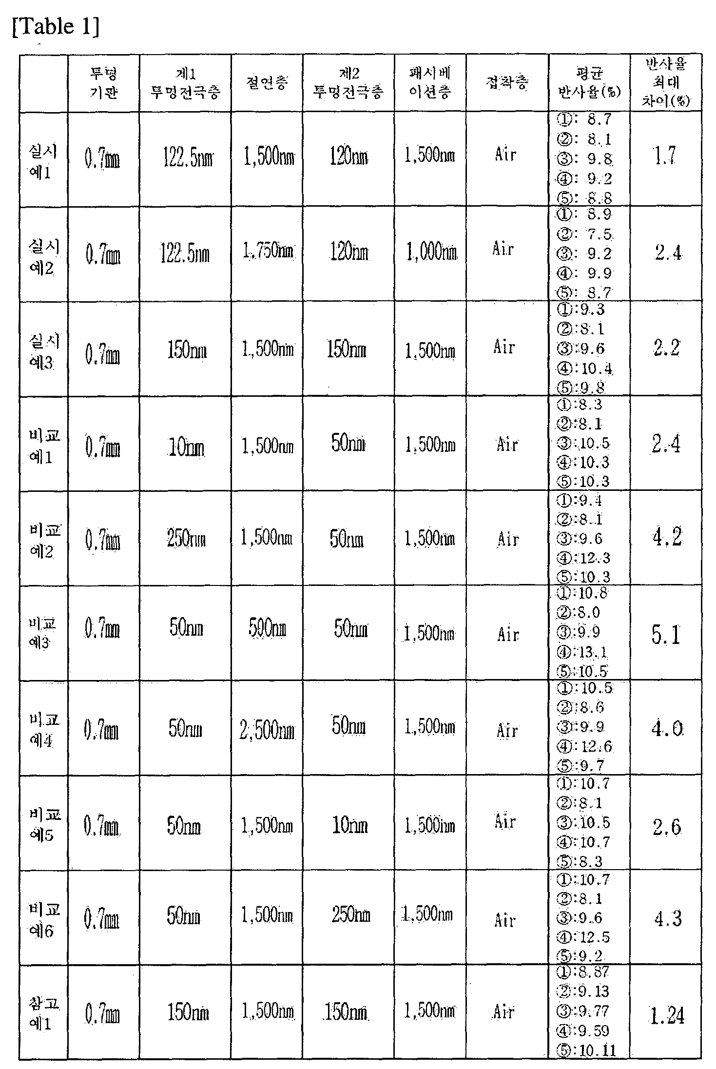
표 2
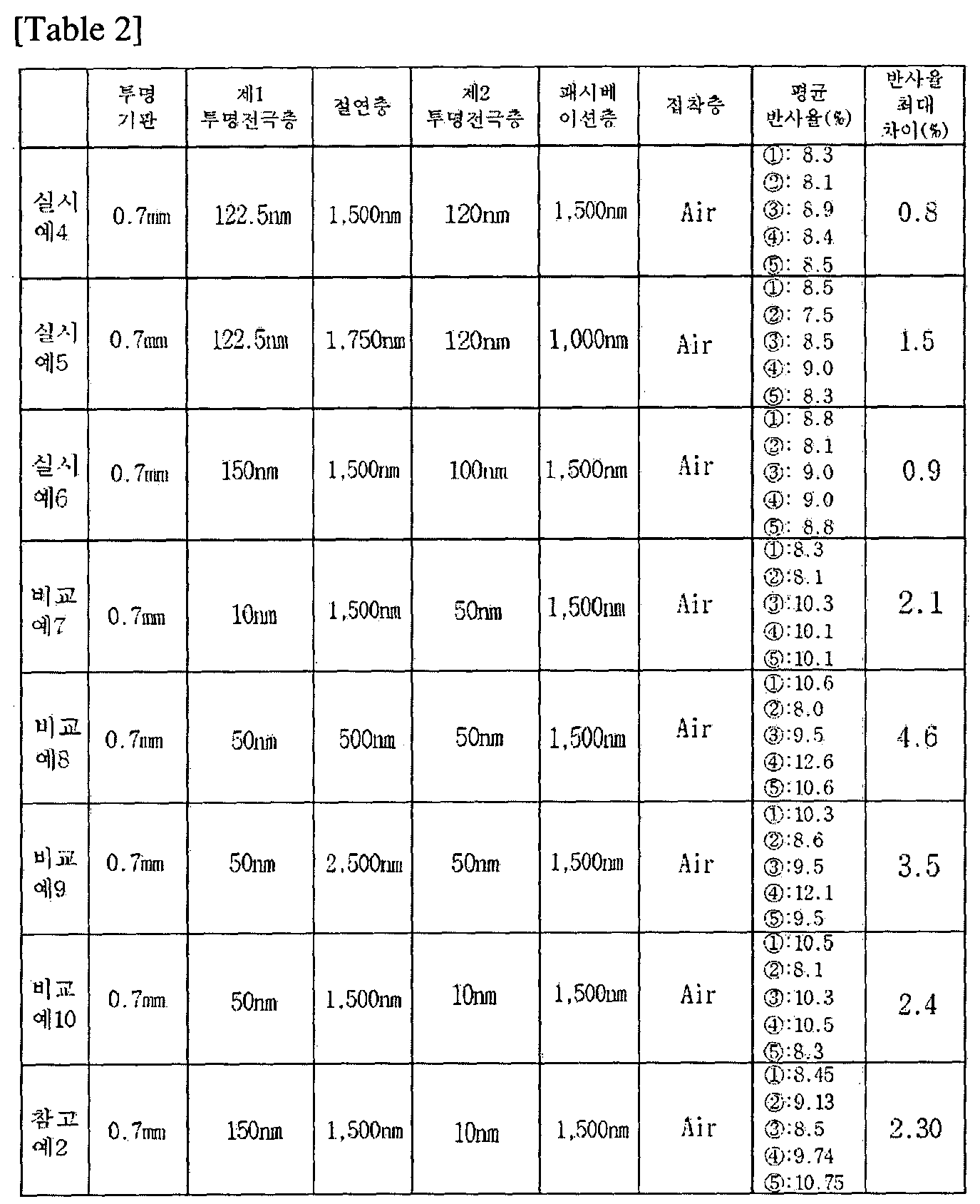
표 3

표 4

Claims (11)
- 투명 기판 상에 각각 미리 정해진 패턴으로 적층되는 제1 투명전극층 및 제2 투명전극층, 상기 제1 투명전극층과 제2 투명전극층 사이에 개재된 절연층, 상기 절연층에 형성되어 상기 제1 투명전극층과 제2 투명전극층을 전기적으로 연결하는 콘택홀을 포함하며,상기 제1 투명전극층과 제2 투명전극층은 각각 그 두께가 100 내지 200nm이고,상기 절연층은 그 두께가 1,000 내지 2,000nm인 투명 전극 적층체.
- 청구항 1에 있어서, 상기 제1 투명전극층 및 제2 투명전극층은 각각 굴절률이 1.8 내지 1.98인 투명 전극 적층체.
- 청구항 1에 있어서, 상기 절연층은 굴절률이 1.4 내지 1.6인 투명 전극 적층체.
- 청구항 1에 있어서, 상기 투명 기판은 두께가 0.1 내지 0.7mm인 투명 전극 적층체.
- 청구항 1에 있어서, 상기 투명 기판은 굴절률이 1.4 내지 1.6인 투명 전극 적층체.
- 청구항 1에 있어서, 투명 전극 적층체를 기준으로 상기 투명 기판의 반대쪽 면 측에 패시베이션층을 더 구비하는 투명 전극 적층체.
- 청구항 6에 있어서, 상기 패시베이션층은 두께가 2,000nm 이하인 투명 전극 적층체.
- 청구항 6에 있어서, 상기 패시베이션층은 굴절률이 1.4 내지 1.6인 투명 전극 적층체.
- 청구항 1에 있어서, 상기 투명 기판은 투명 전극이 형성되는 면의 반대면에 적어도 1층의 광학기능층을 더 구비하는 투명 전극 적층체.
- 청구항 9에 있어서, 상기 광학기능층은 반사방지층 및 오염방지층 중 적어도 1층인 투명 전극 적층체.
- 청구항 1 내지 10 중 어느 한 항의 투명 전극 적층체를 구비한 터치 스크린 패널.
Priority Applications (3)
| Application Number | Priority Date | Filing Date | Title |
|---|---|---|---|
| US14/779,425 US9760228B2 (en) | 2013-03-29 | 2014-02-21 | Transparent electrode pattern structure and touch screen panel including the same |
| CN201480017304.7A CN105164620B (zh) | 2013-03-29 | 2014-02-21 | 透明电极图案层压体以及具备该层压体的触摸屏面板 |
| JP2016505379A JP6533214B2 (ja) | 2013-03-29 | 2014-02-21 | 透明電極パターン積層体及びこれを備えたタッチスクリーンパネル |
Applications Claiming Priority (2)
| Application Number | Priority Date | Filing Date | Title |
|---|---|---|---|
| KR1020130034792A KR101879220B1 (ko) | 2013-03-29 | 2013-03-29 | 투명 전극 패턴 적층체 및 이를 구비한 터치 스크린 패널 |
| KR10-2013-0034792 | 2013-03-29 |
Publications (1)
| Publication Number | Publication Date |
|---|---|
| WO2014157841A1 true WO2014157841A1 (ko) | 2014-10-02 |
Family
ID=51624755
Family Applications (1)
| Application Number | Title | Priority Date | Filing Date |
|---|---|---|---|
| PCT/KR2014/001408 Ceased WO2014157841A1 (ko) | 2013-03-29 | 2014-02-21 | 투명 전극 패턴 적층체 및 이를 구비한 터치 스크린 패널 |
Country Status (6)
| Country | Link |
|---|---|
| US (1) | US9760228B2 (ko) |
| JP (1) | JP6533214B2 (ko) |
| KR (1) | KR101879220B1 (ko) |
| CN (1) | CN105164620B (ko) |
| TW (1) | TWI584180B (ko) |
| WO (1) | WO2014157841A1 (ko) |
Cited By (1)
| Publication number | Priority date | Publication date | Assignee | Title |
|---|---|---|---|---|
| WO2017010816A1 (ko) * | 2015-07-14 | 2017-01-19 | 주식회사 엘지화학 | 전도성 구조체, 이의 제조방법, 이를 포함하는 터치패널 및 이를 포함하는 디스플레이 장치 |
Families Citing this family (8)
| Publication number | Priority date | Publication date | Assignee | Title |
|---|---|---|---|---|
| JP5964273B2 (ja) * | 2013-05-27 | 2016-08-03 | 日東電工株式会社 | タッチパネルセンサ |
| CN106066720B (zh) | 2015-04-22 | 2019-04-26 | 财团法人工业技术研究院 | 感应装置 |
| CN106066747A (zh) | 2015-04-22 | 2016-11-02 | 财团法人工业技术研究院 | 具触控功能的光学薄膜 |
| TWI746603B (zh) * | 2016-08-09 | 2021-11-21 | 南韓商東友精細化工有限公司 | 透明電極、包括其的觸控感測器及影像顯示裝置 |
| KR102392231B1 (ko) | 2016-12-02 | 2022-04-28 | 알프스 알파인 가부시키가이샤 | 투명 전극 부재 및 그 제조 방법, 그리고 그 투명 전극 부재를 사용한 정전 용량식 센서 |
| KR102430032B1 (ko) * | 2017-08-16 | 2022-08-04 | 동우 화인켐 주식회사 | 투명 전극 적층체 및 이의 제조 방법 |
| DE102019101764A1 (de) * | 2019-01-24 | 2020-07-30 | Bayerische Motoren Werke Aktiengesellschaft | Modul für eine Anzeige- und/oder Bedienvorrichtung, Anzeige- und/oder Bedienvorrichtung, Verfahren zur Herstellung eines Moduls und Fortbewegungsmittel |
| CN115989473A (zh) | 2020-08-24 | 2023-04-18 | 东友精细化工有限公司 | 触摸传感器和包含其的层叠体 |
Citations (5)
| Publication number | Priority date | Publication date | Assignee | Title |
|---|---|---|---|---|
| KR20010033970A (ko) * | 1998-01-09 | 2001-04-25 | 니폰샤신인사츠가부시키가이샤 | 터치입력방식의 액정표시장치 및 그 제조방법 |
| KR20070042506A (ko) * | 2004-08-17 | 2007-04-23 | 도레이 가부시끼가이샤 | 터치패널용 복합 투명도전성 기재 및 터치패널 |
| US20070132927A1 (en) * | 2005-12-12 | 2007-06-14 | Sanyo Epson Imaging Devices Corporation | Liquid crystal device and electronic apparatus |
| KR20100044726A (ko) * | 2008-10-22 | 2010-04-30 | 삼성엘이디 주식회사 | 반도체 발광 소자 |
| WO2012111519A1 (ja) * | 2011-02-15 | 2012-08-23 | シャープ株式会社 | タッチパネル及び該タッチパネルを備えた表示装置 |
Family Cites Families (13)
| Publication number | Priority date | Publication date | Assignee | Title |
|---|---|---|---|---|
| JP2005179481A (ja) | 2003-12-18 | 2005-07-07 | Nitto Denko Corp | 積層シート及び液晶表示装置 |
| US8603611B2 (en) | 2005-05-26 | 2013-12-10 | Gunze Limited | Transparent planar body and transparent touch switch |
| JP4998919B2 (ja) * | 2007-06-14 | 2012-08-15 | ソニーモバイルディスプレイ株式会社 | 静電容量型入力装置 |
| CN101576793A (zh) * | 2009-01-12 | 2009-11-11 | 深圳市中显微电子有限公司 | 一种电容式触摸屏及其制作方法 |
| KR101351415B1 (ko) | 2009-12-09 | 2014-01-16 | 엘지디스플레이 주식회사 | 터치 패널 및 터치 패널 일체형 액정 표시 장치 |
| US8493349B2 (en) * | 2009-12-10 | 2013-07-23 | Lg Display Co., Ltd. | Touch screen panel |
| JP2012081663A (ja) * | 2010-10-12 | 2012-04-26 | Sumitomo Metal Mining Co Ltd | 透明導電基材及びタッチパネル |
| EP2638453A4 (en) * | 2010-11-09 | 2015-11-25 | Tpk Touch Solutions Inc | Touch panel device |
| JP5699352B2 (ja) * | 2010-11-11 | 2015-04-08 | 北川工業株式会社 | 透明導電フィルム |
| JP2012203701A (ja) * | 2011-03-25 | 2012-10-22 | Dainippon Printing Co Ltd | タッチパネル部材、透明電極層付き基板、基板積層型タッチパネル部材、および、上記タッチパネル部材または上記基板積層型タッチパネル部材を用いた座標検出装置 |
| TW201250529A (en) | 2011-06-07 | 2012-12-16 | Mutto Optronics Corp | Touch panel having insulators |
| EP2680111A4 (en) * | 2011-11-11 | 2014-02-26 | Kaneka Corp | SUBSTRATE HAVING TRANSPARENT ELECTRODE, PRODUCTION METHOD THEREFOR, AND TOUCH SCREEN |
| TWM461102U (zh) | 2013-03-12 | 2013-09-01 | Emerging Display Tech Corp | 避免電極顯現的雙板式觸控面板 |
-
2013
- 2013-03-29 KR KR1020130034792A patent/KR101879220B1/ko active Active
-
2014
- 2014-02-21 CN CN201480017304.7A patent/CN105164620B/zh active Active
- 2014-02-21 US US14/779,425 patent/US9760228B2/en active Active
- 2014-02-21 JP JP2016505379A patent/JP6533214B2/ja active Active
- 2014-02-21 WO PCT/KR2014/001408 patent/WO2014157841A1/ko not_active Ceased
- 2014-03-24 TW TW103110858A patent/TWI584180B/zh active
Patent Citations (5)
| Publication number | Priority date | Publication date | Assignee | Title |
|---|---|---|---|---|
| KR20010033970A (ko) * | 1998-01-09 | 2001-04-25 | 니폰샤신인사츠가부시키가이샤 | 터치입력방식의 액정표시장치 및 그 제조방법 |
| KR20070042506A (ko) * | 2004-08-17 | 2007-04-23 | 도레이 가부시끼가이샤 | 터치패널용 복합 투명도전성 기재 및 터치패널 |
| US20070132927A1 (en) * | 2005-12-12 | 2007-06-14 | Sanyo Epson Imaging Devices Corporation | Liquid crystal device and electronic apparatus |
| KR20100044726A (ko) * | 2008-10-22 | 2010-04-30 | 삼성엘이디 주식회사 | 반도체 발광 소자 |
| WO2012111519A1 (ja) * | 2011-02-15 | 2012-08-23 | シャープ株式会社 | タッチパネル及び該タッチパネルを備えた表示装置 |
Cited By (2)
| Publication number | Priority date | Publication date | Assignee | Title |
|---|---|---|---|---|
| WO2017010816A1 (ko) * | 2015-07-14 | 2017-01-19 | 주식회사 엘지화학 | 전도성 구조체, 이의 제조방법, 이를 포함하는 터치패널 및 이를 포함하는 디스플레이 장치 |
| US10528167B2 (en) | 2015-07-14 | 2020-01-07 | Lg Chem, Ltd. | Conductive structure, method for manufacturing same, touch panel comprising same and display device comprising same |
Also Published As
| Publication number | Publication date |
|---|---|
| CN105164620A (zh) | 2015-12-16 |
| CN105164620B (zh) | 2019-04-02 |
| US20160048242A1 (en) | 2016-02-18 |
| TW201441907A (zh) | 2014-11-01 |
| US9760228B2 (en) | 2017-09-12 |
| JP2016514873A (ja) | 2016-05-23 |
| KR20140118593A (ko) | 2014-10-08 |
| KR101879220B1 (ko) | 2018-07-17 |
| TWI584180B (zh) | 2017-05-21 |
| JP6533214B2 (ja) | 2019-06-19 |
Similar Documents
| Publication | Publication Date | Title |
|---|---|---|
| WO2014157841A1 (ko) | 투명 전극 패턴 적층체 및 이를 구비한 터치 스크린 패널 | |
| WO2014189204A1 (ko) | 투명 전극 패턴 적층체 및 이를 구비한 터치 스크린 패널 | |
| WO2012015284A2 (en) | Touch panel | |
| WO2013002609A2 (en) | Touch panel and method for manufacturing the same | |
| WO2013062385A1 (en) | Touch panel | |
| WO2012099394A2 (en) | Touch panel and method for manufacturing the same | |
| WO2014021629A1 (ko) | 반사방지층을 포함하는 센서 패널 및 그 제조 방법 | |
| WO2015076505A1 (ko) | 복합 편광판 일체형 터치 감지 전극 및 이를 구비한 터치 스크린 패널 | |
| WO2019168303A1 (ko) | 터치센서 일체형 디지타이저 및 이를 포함하는 표시 장치 | |
| WO2016159501A1 (ko) | 터치 센서 | |
| US9489914B2 (en) | Transparent electrode laminate and touch screen panel including the same | |
| WO2015174678A1 (ko) | 전도성 구조체 및 이의 제조방법 | |
| WO2015026071A1 (ko) | 터치 감지 전극 및 이를 구비하는 터치 스크린 패널 | |
| WO2015030404A1 (ko) | 터치 감지 전극 및 이를 구비하는 터치 스크린 패널 | |
| KR102077548B1 (ko) | 투명 전극 패턴 적층체 및 이를 구비한 터치 스크린 패널 | |
| WO2015046769A1 (ko) | 터치 감지 전극 및 이를 구비하는 터치 스크린 패널 | |
| WO2016093517A1 (ko) | 터치 스크린 패널 및 이를 구비하는 화상표시장치 | |
| WO2014178545A1 (ko) | 터치 패널 및 제조 방법 | |
| CN105468184B (zh) | 透明电极层压体和包括该透明电极层压体的触摸屏面板 | |
| TW201512943A (zh) | 觸感電極 | |
| WO2019168362A1 (ko) | 디지타이저 및 그 제조 방법 | |
| WO2014084696A1 (ko) | 전도성 기판 및 이의 제조방법 | |
| WO2012047013A2 (ko) | 정전용량방식 터치 패널 소자 및 이의 제조방법 | |
| WO2015069048A1 (ko) | 한 장의 필름을 이용한 터치 센서를 구현하는 터치 패널 및 제조 방법 | |
| WO2014178546A1 (ko) | 터치 패널 및 이의 제조 방법 |
Legal Events
| Date | Code | Title | Description |
|---|---|---|---|
| WWE | Wipo information: entry into national phase |
Ref document number: 201480017304.7 Country of ref document: CN |
|
| 121 | Ep: the epo has been informed by wipo that ep was designated in this application |
Ref document number: 14775391 Country of ref document: EP Kind code of ref document: A1 |
|
| ENP | Entry into the national phase |
Ref document number: 2016505379 Country of ref document: JP Kind code of ref document: A |
|
| WWE | Wipo information: entry into national phase |
Ref document number: 14779425 Country of ref document: US |
|
| NENP | Non-entry into the national phase |
Ref country code: DE |
|
| 122 | Ep: pct application non-entry in european phase |
Ref document number: 14775391 Country of ref document: EP Kind code of ref document: A1 |