WO2014157000A1 - 炭素ドープ酸化亜鉛膜及びその製造方法 - Google Patents
炭素ドープ酸化亜鉛膜及びその製造方法 Download PDFInfo
- Publication number
- WO2014157000A1 WO2014157000A1 PCT/JP2014/057877 JP2014057877W WO2014157000A1 WO 2014157000 A1 WO2014157000 A1 WO 2014157000A1 JP 2014057877 W JP2014057877 W JP 2014057877W WO 2014157000 A1 WO2014157000 A1 WO 2014157000A1
- Authority
- WO
- WIPO (PCT)
- Prior art keywords
- carbon
- zinc oxide
- oxide film
- concentration
- doped
- Prior art date
- Legal status (The legal status is an assumption and is not a legal conclusion. Google has not performed a legal analysis and makes no representation as to the accuracy of the status listed.)
- Ceased
Links
Images


Classifications
-
- C—CHEMISTRY; METALLURGY
- C30—CRYSTAL GROWTH
- C30B—SINGLE-CRYSTAL GROWTH; UNIDIRECTIONAL SOLIDIFICATION OF EUTECTIC MATERIAL OR UNIDIRECTIONAL DEMIXING OF EUTECTOID MATERIAL; REFINING BY ZONE-MELTING OF MATERIAL; PRODUCTION OF A HOMOGENEOUS POLYCRYSTALLINE MATERIAL WITH DEFINED STRUCTURE; SINGLE CRYSTALS OR HOMOGENEOUS POLYCRYSTALLINE MATERIAL WITH DEFINED STRUCTURE; AFTER-TREATMENT OF SINGLE CRYSTALS OR A HOMOGENEOUS POLYCRYSTALLINE MATERIAL WITH DEFINED STRUCTURE; APPARATUS THEREFOR
- C30B29/00—Single crystals or homogeneous polycrystalline material with defined structure characterised by the material or by their shape
- C30B29/10—Inorganic compounds or compositions
- C30B29/16—Oxides
-
- C—CHEMISTRY; METALLURGY
- C23—COATING METALLIC MATERIAL; COATING MATERIAL WITH METALLIC MATERIAL; CHEMICAL SURFACE TREATMENT; DIFFUSION TREATMENT OF METALLIC MATERIAL; COATING BY VACUUM EVAPORATION, BY SPUTTERING, BY ION IMPLANTATION OR BY CHEMICAL VAPOUR DEPOSITION, IN GENERAL; INHIBITING CORROSION OF METALLIC MATERIAL OR INCRUSTATION IN GENERAL
- C23C—COATING METALLIC MATERIAL; COATING MATERIAL WITH METALLIC MATERIAL; SURFACE TREATMENT OF METALLIC MATERIAL BY DIFFUSION INTO THE SURFACE, BY CHEMICAL CONVERSION OR SUBSTITUTION; COATING BY VACUUM EVAPORATION, BY SPUTTERING, BY ION IMPLANTATION OR BY CHEMICAL VAPOUR DEPOSITION, IN GENERAL
- C23C14/00—Coating by vacuum evaporation, by sputtering or by ion implantation of the coating forming material
- C23C14/06—Coating by vacuum evaporation, by sputtering or by ion implantation of the coating forming material characterised by the coating material
- C23C14/08—Oxides
- C23C14/086—Oxides of zinc, germanium, cadmium, indium, tin, thallium or bismuth
-
- C—CHEMISTRY; METALLURGY
- C30—CRYSTAL GROWTH
- C30B—SINGLE-CRYSTAL GROWTH; UNIDIRECTIONAL SOLIDIFICATION OF EUTECTIC MATERIAL OR UNIDIRECTIONAL DEMIXING OF EUTECTOID MATERIAL; REFINING BY ZONE-MELTING OF MATERIAL; PRODUCTION OF A HOMOGENEOUS POLYCRYSTALLINE MATERIAL WITH DEFINED STRUCTURE; SINGLE CRYSTALS OR HOMOGENEOUS POLYCRYSTALLINE MATERIAL WITH DEFINED STRUCTURE; AFTER-TREATMENT OF SINGLE CRYSTALS OR A HOMOGENEOUS POLYCRYSTALLINE MATERIAL WITH DEFINED STRUCTURE; APPARATUS THEREFOR
- C30B23/00—Single-crystal growth by condensing evaporated or sublimed materials
- C30B23/02—Epitaxial-layer growth
-
- H—ELECTRICITY
- H10—SEMICONDUCTOR DEVICES; ELECTRIC SOLID-STATE DEVICES NOT OTHERWISE PROVIDED FOR
- H10P—GENERIC PROCESSES OR APPARATUS FOR THE MANUFACTURE OR TREATMENT OF DEVICES COVERED BY CLASS H10
- H10P14/00—Formation of materials, e.g. in the shape of layers or pillars
- H10P14/20—Formation of materials, e.g. in the shape of layers or pillars of semiconductor materials
- H10P14/29—Formation of materials, e.g. in the shape of layers or pillars of semiconductor materials characterised by the substrates
- H10P14/2901—Materials
- H10P14/2921—Materials being crystalline insulating materials
-
- H—ELECTRICITY
- H10—SEMICONDUCTOR DEVICES; ELECTRIC SOLID-STATE DEVICES NOT OTHERWISE PROVIDED FOR
- H10P—GENERIC PROCESSES OR APPARATUS FOR THE MANUFACTURE OR TREATMENT OF DEVICES COVERED BY CLASS H10
- H10P14/00—Formation of materials, e.g. in the shape of layers or pillars
- H10P14/20—Formation of materials, e.g. in the shape of layers or pillars of semiconductor materials
- H10P14/34—Deposited materials, e.g. layers
- H10P14/3402—Deposited materials, e.g. layers characterised by the chemical composition
- H10P14/3424—Deposited materials, e.g. layers characterised by the chemical composition being Group IIB-VIA materials
- H10P14/3426—Oxides
-
- H—ELECTRICITY
- H10—SEMICONDUCTOR DEVICES; ELECTRIC SOLID-STATE DEVICES NOT OTHERWISE PROVIDED FOR
- H10P—GENERIC PROCESSES OR APPARATUS FOR THE MANUFACTURE OR TREATMENT OF DEVICES COVERED BY CLASS H10
- H10P14/00—Formation of materials, e.g. in the shape of layers or pillars
- H10P14/20—Formation of materials, e.g. in the shape of layers or pillars of semiconductor materials
- H10P14/34—Deposited materials, e.g. layers
- H10P14/3438—Doping during depositing
- H10P14/3441—Conductivity type
- H10P14/3444—P-type
Definitions
- the present invention relates to a carbon-doped zinc oxide film and a method for producing the same.
- ZnO is attracting attention as a new thin film material succeeding this.
- ZnO is a direct transition type semiconductor with a band gap energy of about 3.4 eV and a high exciton binding energy of about 60 meV, so it is possible to realize a highly efficient light-emitting device with low power consumption and excellent environmental performance.
- GaN and AlGaNIn it does not contain rare metals such as Ga and In, and therefore has features such as being inexpensive and harmless to the environment and the human body.
- a light-emitting element is formed by forming a pn junction composed of a p-type semiconductor and an n-type semiconductor on a substrate, it is necessary to form a p-type semiconductor and an n-type semiconductor on the substrate in order to manufacture the light-emitting element. .
- ZnO is very likely to cause oxygen vacancies, it tends to be an n-type semiconductor as a result.
- Various methods have been reported as methods for forming p-type semiconductor ZnO, but there is no technology that has been developed so that its characteristics are stably expressed and can be used industrially.
- dopants and one of them is a method of doping carbon (C).
- Patent Document 1 Japanese Patent Laid-Open No. 2005-243955 discusses the preparation of p-type ZnO by metal organic vapor phase epitaxy (hereinafter referred to as MOVPE) or molecular beam epitaxy (hereinafter referred to as MBE). Further, it is described that the C concentration is adjusted to 1 ⁇ 10 16 to 1 ⁇ 10 20 cm ⁇ 3 , and it is described that it is extremely difficult to achieve a concentration exceeding 1 ⁇ 10 20 cm ⁇ 3. ing. Further, it is described that when N is mixed, N is activated and stabilized as an acceptor, and p-type carriers are generated efficiently and stably, and the N concentration is 1 ⁇ 10 16 to 1 ⁇ 10 19 cm ⁇ . The adjustment in the range of 3 is described, and it is described that it is preferable for obtaining good p-type characteristics.
- MOVPE metal organic vapor phase epitaxy
- MBE molecular beam epitaxy
- Patent Document 2 Japanese Patent Laid-Open No. 8-222765 discloses that a p-type II-VI group compound semiconductor containing nitrogen and carbon of 1 ⁇ 10 17 cm ⁇ 3 or more is prepared by MBE growth. Has been.
- ZnS, ZnSe, etc. are used as II-VI group compound semiconductors, but no mention or evaluation is made on ZnO.
- the present inventors have now found that a zinc oxide film doped with carbon at a high concentration can be reliably produced and provided by a relatively simple and inexpensive method.
- an object of the present invention is to reliably manufacture and provide a zinc oxide film doped with carbon at a high concentration by a relatively simple and inexpensive method.
- the carbon produced by at least one film forming method selected from a sputtering method and a PLD (pulse laser deposition) method is 1.0 ⁇ 10 19 atoms / cm 3 or more.
- a carbon-doped zinc oxide film which is a film made of polycrystalline zinc oxide doped at a concentration of.
- a method for producing a carbon-doped zinc oxide film comprising: Preparing a composite target having zinc, oxygen, and carbon as constituent elements; Forming a film by at least one of a sputtering method and a PLD method using the composite target, thereby forming the carbon-doped zinc oxide film; A method is provided comprising.
- Example 2 it is a figure which shows C density
- FIG. 2 it is a figure which shows N density
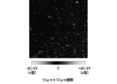
- FIG. 3 is an XRD profile measured for Sample 1 in Example 3. It is a SCM image (p / n polarity image) measured from the film
- FIG. 1 It is a SCM image (p / n polarity image) measured from the film
- Carbon-doped zinc oxide film of the present invention is produced by at least one film forming method selected from a sputtering method and a PLD method, and has a carbon content of 1.0 ⁇ 10 19 atoms / cm 3. It is a film made of zinc oxide polycrystals doped at a high concentration as described above, and preferably consists essentially of (or consists only of) such zinc oxide polycrystals. Since carbon can function as an acceptor, doping the carbon in the zinc oxide film at a high concentration in this way increases the hole concentration in the zinc oxide film and exhibits higher p-type characteristics. Nevertheless, it has been difficult to say that such a method of doping a high concentration of carbon has been well established.
- Patent Document 1 teaches that carbon is doped in a concentration range of 1 ⁇ 10 16 to 1 ⁇ 10 20 cm ⁇ 3 in order to obtain p-type ZnO, but the upper limit of 1 ⁇ is actually set. There is no empirical data showing that carbon is doped at a high concentration in the vicinity of 10 20 cm ⁇ 3 .
- the MOVPE method and the MBE method adopted in Patent Document 1 are both methods that require very expensive equipment, which may lead to an increase in manufacturing cost, and are less expensive than rare metals such as Ga and In. The advantage of zinc oxide that it is a simple material cannot be fully enjoyed.
- the present invention is based on the knowledge that a high concentration of carbon can be reliably doped into a zinc oxide film by using a relatively simple sputtering method or PLD method as a vapor phase method.
- the reason why high-concentration carbon can be reliably doped by the sputtering method or PLD method is unclear, but it is doped into zinc oxide because the carbon to be sputtered has high energy or through the plasma.
- the volatilized component is likely to be doped into zinc oxide through the plasma plume.
- the carbon-doped zinc oxide film of the present invention is reliably doped with high-concentration carbon due to the effects of the sputtering method and the PLD method, which is an expensive device required for the MOVPE method and the MBE method.
- a wide range of industrial applications can be expected as an inexpensive film exhibiting high p-type characteristics, coupled with the advantages of zinc oxide, which can reduce the manufacturing cost by eliminating the need for use, and is an inherently inexpensive material.
- the concentration of carbon contained in the zinc oxide polycrystal is 1.0 ⁇ 10 19 atoms / cm 3 or more, preferably higher than 1.0 ⁇ 10 20 atoms / cm 3 , more preferably 1.1 ⁇ 10 20 atoms / cm 3 or more, particularly preferably 1.2 ⁇ 10 20 atoms / cm 3 or more. Since carbon can function as an acceptor, higher concentration range as described above can increase the hole concentration in the zinc oxide film and realize higher p-type characteristics.
- the upper limit of the carbon concentration should not be particularly limited, but is preferably 4.1 ⁇ 10 21 atoms / cm 3 or less, more preferably 1 It is considered that good crystallinity will be obtained if the density is 0.0 ⁇ 10 21 atoms / cm 3 or less.
- the zinc oxide polycrystal is preferably further doped with nitrogen, and its concentration is preferably higher than 1.0 ⁇ 10 19 atoms / cm 3 , more preferably 1.1 ⁇ 10 19 atoms / cm 3. 3 or more, more preferably 1.5 ⁇ 10 19 atoms / cm 3 or more. Since nitrogen can also function as an acceptor in the same manner as carbon, by setting the concentration range as described above, the hole concentration in the zinc oxide film can be increased and higher p-type characteristics can be realized.
- the upper limit of the nitrogen concentration should not be particularly limited, but is preferably 4.1 ⁇ 10 21 atoms / cm 3 or less, more preferably 1 It is considered that good crystallinity will be obtained if the density is 0.0 ⁇ 10 21 atoms / cm 3 or less. However, when the desired performance is sufficiently secured at a carbon concentration higher than 1.0 ⁇ 10 20 atoms / cm 3 , the nitrogen concentration is 1.0 ⁇ 10 19 atoms / cm 3 or less. Also good.
- the carbon-doped zinc oxide film of the present invention is a film made of zinc oxide polycrystal due to being manufactured by a sputtering method or a PLD method.
- the above-described dopants such as carbon and nitrogen are preferably dissolved in the individual crystallites constituting the zinc oxide polycrystal, but desired p-type characteristics can be obtained. As long as it exists, it may exist in arbitrary positions including the grain boundary of crystallites.
- the carbon-doped zinc oxide film of the present invention is preferably formed by c-axis orientation of the zinc oxide polycrystal constituting the film in the direction perpendicular to the film surface.
- c-axis orientation in the direction perpendicular to the film surface means that the (002) plane diffraction peak intensity excluding the base line when the XRD diffraction measurement is performed from above the film has the same zinc oxide excluding the base line. It is defined as an orientation state that is 5 times or more with respect to diffraction intensity other than the c-plane.
- the thickness of the carbon-doped zinc oxide film of the present invention is not particularly limited as long as the thickness capable of obtaining desired characteristics is appropriately selected, but is preferably 0.001 to 10 ⁇ m, more preferably 0.005 to 3 ⁇ m. More preferably, the thickness is 0.01 to 2 ⁇ m.
- the carbon-doped zinc oxide film of the present invention is manufactured by a film forming method using at least one of a sputtering method and a PLD method.
- a sputtering method and the PLD method are relatively simple methods as the gas phase method, it is possible to reduce the manufacturing cost by eliminating the need for expensive equipment required for the MOVPE method and the MBE method. . Nevertheless, a high concentration of carbon can be reliably doped into the zinc oxide film.
- the reason why high-concentration carbon can be reliably doped by the sputtering method or the PLD method is unclear, but in the sputtering method, the sputtered carbon has high energy, and the carbon is oxidized by passing through the plasma.
- the method of the present invention not only has the advantage that high concentration of carbon can be reliably doped due to the influence of the sputtering method and the PLD method, but also has the advantage of zinc oxide that is an inherently inexpensive material. Together with this, it is possible to manufacture an inexpensive carbon-doped zinc oxide film exhibiting high p-type characteristics, and to give a wide range of industrial application possibilities to the p-type zinc oxide film.
- the manufacturing method of the present invention includes a step of preparing a composite target (in this case, a composite sputtering target) containing zinc, oxygen, and carbon as constituent elements, and performing sputtering using this target, thereby carbon doping Forming a zinc oxide film.
- a composite target in this case, a composite sputtering target
- the production method of the present invention is a step of preparing a composite sputtering target comprising a sintered body containing zinc oxide as a main component and containing or having carbon in or on the surface of the sintered body. And sputtering using this composite sputtering target, thereby forming a carbon-doped zinc oxide film.
- the manufacturing method of the present invention includes a step of preparing a composite target (in this case, a composite PLD target) containing zinc, oxygen, and carbon as constituent elements, and performing film formation by the PLD method using this target. And thereby forming a carbon-doped zinc oxide film.
- the production method of the present invention is a step of preparing a composite PLD target comprising a sintered body containing zinc oxide as a main component and containing or having carbon in or on the surface of the sintered body. And forming a film using the composite PLD target, thereby forming a carbon-doped zinc oxide film.
- the composite target used in the method of the present invention is at least one of a composite sputtering target and a composite PLD target, and can be configured in any form as long as it contains zinc, oxygen, and carbon as constituent elements.
- it can be a sintered body made of zinc oxide and carbon, an aggregate of zinc oxide pieces and carbon pieces, or an aggregate of zinc oxide pieces, zinc pieces and carbon pieces.
- these sintered compacts and pieces may contain a required amount of dopant elements such as carbon and nitrogen.
- a typical composite sputtering target and composite PLD target are made of a sintered body containing zinc oxide as a main component, and contain or include carbon in the sintered body or on the surface thereof.
- the sintered body containing zinc oxide as a main component is preferably a zinc oxide sintered body, more preferably a purity of 99.9% or more, and further preferably a purity of 99.99. Although it is a zinc oxide sintered body having a purity of 99%, particularly preferably 99.999% or more, it may contain a required amount of a dopant element such as carbon or nitrogen.
- the composite sputtering target and the composite PLD target contain carbon in a zinc oxide-based sintered body.
- a zinc oxide-based sintered body containing carbon can be obtained by mixing zinc oxide powder and carbon powder, forming the mixture into a predetermined size, and sintering in an inert atmosphere. it can.
- the inert atmosphere include N 2 , Ar, He and the like.
- the composite sputtering target and the composite PLD target include a carbon layer on a part of the surface of the zinc oxide-based sintered body.
- a composite target can be obtained simply by placing or laminating a carbon layer on a zinc oxide sintered compact target, which is extremely simple.
- the carbon layer may be a layered material such as a carbon sheet, film, or plate.
- the carbon layer is also preferably highly pure, more preferably 99% or more, and even more preferably 99.9% or more.
- the carbon layer is configured to cover only a part of the surface of the zinc oxide and to partially expose the zinc oxide to the surface so that the zinc oxide is simultaneously sputtered or ablated.
- the carbon layer may be configured to have an area smaller than the area of the zinc oxide-based sintered body, or may be configured only on the outer peripheral portion of the zinc oxide-based sintered body.
- an open carbon layer may be used. In any case, the amount of carbon doping can be appropriately adjusted by controlling the area of the carbon layer covering the surface of the zinc oxide sintered body.
- the composite sputtering target and the composite PLD target may be an aggregate of zinc oxide pieces and carbon pieces.
- a composite target can be obtained simply by arranging zinc oxide pieces and carbon pieces in an arbitrary layout (for example, mosaic shape), which is extremely simple.
- Sputtering is performed using a composite sputtering target, whereby a carbon-doped zinc oxide film can be formed.
- the method of sputtering is not particularly limited as long as it is a method in which atoms constituting a solid are ejected and adhered to the object surface of the substrate when ions are irradiated onto the solid surface. Examples include radio frequency (RF) magnetron sputtering, direct current (DC) magnetron sputtering, RF sputtering, DC sputtering, ion beam sputter deposition, ECR sputtering, ion plating, and the like. From the viewpoint of sex.
- sputtering conditions may be performed in accordance with known sputtering conditions, and are not particularly limited.
- nitrogen in the atmosphere serves as a supply source. Therefore, the amount of nitrogen doped can be appropriately adjusted by appropriately controlling the ultimate vacuum in the vacuuming performed before sputtering.
- Such ultimate vacuum is not particularly limited as long as a desired amount of nitrogen doping is obtained, but is preferably 1.0 ⁇ 10 ⁇ 3 Pa to 1.0 ⁇ 10 ⁇ 6 Pa, more preferably 1 0.0 ⁇ 10 ⁇ 4 Pa to 1.0 ⁇ 10 ⁇ 5 Pa.
- nitrogen can be a source of atmospheric gas species during film formation, nitrogen may be introduced as a gas species during film formation if plasma is formed. However, there is no problem even if the value falls below the lower limit of the above preferred range.
- the gas pressure during film formation is not particularly limited as long as a desired amount of nitrogen dope can be obtained. For example, it is preferably 0.01 to 100 Pa, more preferably 0.05 to 10 Pa.
- a composite PLD target can be used to form a carbon-doped zinc oxide film.
- the PLD method is not particularly limited, and preferred examples include a single plume method and a multi-plume multi-turn (MPMT) method.
- MPMT multi-plume multi-turn
- Various conditions for the PLD film formation may be performed in accordance with known PLD film formation conditions, and are not particularly limited.
- nitrogen when nitrogen is doped, nitrogen in the atmosphere serves as a supply source. Therefore, the amount of nitrogen doped can be adjusted as appropriate by appropriately controlling the ultimate vacuum in the vacuuming performed before PLD.
- Such ultimate vacuum is not particularly limited as long as a desired amount of nitrogen doping is obtained, but is preferably 1.0 ⁇ 10 ⁇ 3 Pa to 1.0 ⁇ 10 ⁇ 6 Pa, more preferably 1 0.0 ⁇ 10 ⁇ 4 Pa to 1.0 ⁇ 10 ⁇ 5 Pa.
- the atmospheric gas species during film formation can be a source of nitrogen
- the gas species during film formation may be nitrogen.
- the ultimate vacuum before PLD is below the lower limit of the above preferred range.
- the gas pressure during film formation is not particularly limited as long as a desired amount of nitrogen dope can be obtained. For example, it is preferably 0.01 to 100 Pa, more preferably 0.1 to 30 Pa.
- the obtained carbon-doped zinc oxide film may be heat-treated (annealed), whereby the crystallinity can be improved.
- the heat treatment (annealing) atmosphere is preferably an atmosphere containing oxygen in order to suppress the generation of oxygen vacancies. If the heat treatment (annealing) temperature is too low, defects will not be recovered, and if it is too high, defects will be generated, and this heat treatment (annealing) is preferably performed at 100 to 1000 ° C. for 0.01 to 5 hours. More preferably, it is 300 to 800 ° C. for 0.5 to 5 hours.
- the substrate temperature may be increased in the chamber in the sputtering apparatus as it is, or the heat treatment (annealing) may be performed in another apparatus after the film formation.
- the carbon-doped zinc oxide film may be heat-treated at a high temperature and then subjected to a two-stage heat treatment in which heat treatment is performed in an oxygen-containing atmosphere.
- the first heat treatment at a high temperature is performed to activate carbon and nitrogen contained in the film and enhance the p-type characteristics.
- the atmosphere in which the first heat treatment is performed is not particularly limited, and may be an inert atmosphere such as N 2 or Ar, an oxygen atmosphere, an air atmosphere, or the like.
- the first heat treatment temperature is preferably a high temperature such as 500 to 1000 ° C. in order to activate the dopant. However, when the temperature is maintained for a long time, the dopant carbon or nitrogen is likely to volatilize.
- the temperature maintenance time is short, for example, 10 seconds to 300 seconds.
- the second-stage heat treatment is aimed to recover oxygen deficiency and interstitial zinc deficiency generated in the first-stage heat treatment, and is preferably performed in an oxygen-containing atmosphere. An oxygen atmosphere and an air atmosphere are mentioned. If the heat treatment temperature in the second stage is too low, the defects are not recovered, and if it is too high, defects are generated, and therefore 300 to 800 ° C. is preferable, and the heat treatment time is preferably 0.5 to 5 hours.
- Example 1A Preparation of zinc oxide film by sputtering (samples 1 to 3 and 5 to 8)
- Zinc oxide film samples 1 to 3 and 5 to 8 were produced by sputtering according to the following procedure.
- a high-frequency magnetron sputtering apparatus SPF-210HS, manufactured by Anerva Co., Ltd.
- samples 1 to 3 5 and 6, commercially available c-plane sapphire substrates (purity: 99.99%) were used.
- a commercially available a-plane sapphire substrate was used.
- a commercially available ZnO sputtering target (purity: 99.99% or more) having a diameter of 4 inches (10.16 cm) was prepared, and a commercially available carbon sheet (purity: 99) having an area shown in Table 1 on the sputtering target. .9% or more) was laminated to obtain a ZnO / C composite target.
- the sapphire substrate and the target were respectively set in predetermined holders in the chamber of the sputtering apparatus. Then, sputtering was performed under various conditions such as output, substrate temperature, film formation time, ultimate vacuum, gas pressure, gas type, and gas flow rate shown in Table 1.
- the substrate temperature was raised to the temperature shown in Table 1 in the chamber in the same atmosphere, and annealing was performed for 1 hour.
- the film was taken out, heated to 900 ° C. at 600 ° C./min in a nitrogen atmosphere, held at 900 ° C. for 30 seconds, then cooled to room temperature at 600 ° C./min, and then Then, heat treatment (annealing) was performed for 3.5 hours at 550 ° C. in an air atmosphere.
- Example 4-Comparison For comparison, a zinc oxide film sample 4 was obtained by performing sputtering under various conditions shown in Table 1 in the same procedure as Sample 1 except that the ZnO sputtering target was used as it was without laminating carbon sheets. .
- Example 1B Production of Zinc Oxide Film by PLD Method
- Zinc oxide film samples 9 and 10 were produced by the PLD method according to the following procedure.
- a commercially available a-plane sapphire substrate was used as the substrate.
- the composite PLD target a sintered body produced using a commercially available ZnO powder (purity 99.999%) and a commercially available C powder (purity 99.99%) was used.
- hot press firing was performed in a nitrogen atmosphere at 850 ° C. for 4 hours to obtain a dense ZnO / C composite sintered body. Obtained as a composite PLD target.
- the substrate and the target were respectively set at predetermined positions in the chamber of the PLD apparatus.
- PLD film formation was performed under various conditions such as substrate temperature, film formation time, ultimate vacuum, gas pressure, and gas species shown in Table 2.
- This PLD film formation was performed using a Nd: YAG third harmonic (355 nm) as a laser, a pulse width of 14 to 15 nm, a frequency of 10 Hz, a laser output of 150 mW, and a distance from the substrate of 40 mm.
- Sample 10 was subjected to heat treatment (annealing) at 400 ° C. for 3.5 hours in the air atmosphere after the film formation was completed.
- Example 2 Measurement of concentration of zinc oxide film Dynamic SIMS analysis was performed on the zinc oxide films of Samples 1 to 10 to measure C concentration and N concentration in the zinc oxide film. Note that the dynamic SIMS measurement was performed by using a sample in which the C or N concentration was previously known in zinc oxide as a standard sample. The results of C concentration of Sample 1 and Sample 4 are shown in FIG. 1, and the result of N concentration is shown in FIG. In Table 1, FIG. 1 and FIG. 2, the unit expressed as cm ⁇ 3 means atoms / cm 3 , and the same applies in the following description. 1 and 2, the horizontal axis indicates the depth from the surface, and a value of 0 corresponds to the film surface, and the larger the value, the closer to the substrate side.
- the vertical axis indicates the concentration of each component converted into a standard sample whose C and N concentrations are known in advance in zinc oxide.
- Table 1 shows the concentration of each component averaged in the film thickness direction.
- the region where the influence of contamination is large (for example, in the case of Samples 1 and 4, the region from the surface (0) to 0.05 ⁇ m) is excluded from the average value, and In the region where the concentration of each component sharply decreases on the substrate side, it is considered that ZnO has reached sapphire as the substrate, and this region is also excluded from the average value (the substrate regions of samples 1 and 4 are clearly shown in FIG. 1). .
- Sample 4 as can be seen from FIG.
- the C concentration was 1 ⁇ 10 19 cm ⁇ 3 or less, whereas Sample 1 showed a large value of 1.5 ⁇ 10 20 cm ⁇ 3 .
- the N concentration Sample 1 showed a large value of 1.2 ⁇ 10 20 cm ⁇ 3 .
- Samples 2, 3 and 5 to 10 also have a region where the influence of contamination on the film surface is large by the same method as described above, and a region where the concentration of each component sharply decreases on the substrate side (ie, a region where it appears that the substrate has reached sapphire). Were excluded and averaged to determine C concentration and N concentration.
- the C concentration was higher than 1 ⁇ 10 20 cm ⁇ 3 and the N concentration was higher than 1 ⁇ 10 19 cm ⁇ 3 .
- the C concentration was higher than 1 ⁇ 10 19 cm ⁇ 3 and the N concentration was higher than 1 ⁇ 10 19 cm ⁇ 3 .
- Example 3 Measurement of crystal structure
- the crystal structure was analyzed by X-ray diffraction using an XRD measurement apparatus.
- the results obtained for sample 1 are shown in FIG.
- a strong diffraction peak is observed in the vicinity of 34 °, which is presumed to be a diffraction peak indicating the (002) plane which is the c-plane of ZnO.
- Example 4 pn measurement For samples 9 and 10, pn measurement of a carbon-doped zinc oxide polycrystal was performed using an SCM (scanning capacitance microscope) apparatus. The measurement was performed in the atmosphere at room temperature, the sample was fixed with Ag paste, the modulation voltage was 1 V ( ⁇ 100 kHz), the DC bias voltage was 0 V, and the dC / dV signal was measured. As a result, a portion showing p-type in the film was observed.
- FIG. 4 shows an SCM image (p / n polarity image) obtained for the sample 10 in a visual field range of 10 ⁇ m ⁇ 10 ⁇ m.
- the p-type part is measured as a positive (+) potential and the n-type part is measured as a negative (-) potential.
- the sample 10 is analyzed in more detail and the potential in the measurement range is accumulated, the entire membrane is measured. Since a positive (+) potential was shown, it was found that the entire film was p-type.
- Samples 1 to 3, 5 and 8 have a C concentration greater than 1 ⁇ 10 20 cm ⁇ 3 and an N concentration of 1 ⁇ 10 19 cm ⁇ . It was found that ZnO greater than 3 was obtained. In Samples 6 and 7, it was found that ZnO having a C concentration higher than 1 ⁇ 10 19 cm ⁇ 3 and an N concentration higher than 1 ⁇ 10 19 cm ⁇ 3 was obtained. It was also found that Samples 9 and 10 produced by the PLD method can obtain ZnO having a C concentration higher than 1 ⁇ 10 20 cm ⁇ 3 and an N concentration higher than 1 ⁇ 10 19 cm ⁇ 3 .
- ZnO containing a high concentration of C and N is obtained by using a relatively simple sputtering method as a vapor phase method and laminating and sputtering a carbon sheet on a sputtering target.
- the resulting C and N containing ZnO exhibits higher p-type properties.
- ZnO containing C and N at a high concentration is obtained, so that the obtained C and N-containing ZnO is more Shows high p-type characteristics.
Landscapes
- Chemical & Material Sciences (AREA)
- Engineering & Computer Science (AREA)
- Materials Engineering (AREA)
- Metallurgy (AREA)
- Organic Chemistry (AREA)
- Crystallography & Structural Chemistry (AREA)
- Inorganic Chemistry (AREA)
- Chemical Kinetics & Catalysis (AREA)
- Mechanical Engineering (AREA)
- Physical Vapour Deposition (AREA)
- Crystals, And After-Treatments Of Crystals (AREA)
- Physical Deposition Of Substances That Are Components Of Semiconductor Devices (AREA)
Abstract
スパッタリング法及びPLD法から選択される少なくともいずれか1種の成膜法により製造される、炭素が1.0×10¹⁹atoms/cm3以上の濃度でドープされた酸化亜鉛多結晶からなる膜である、炭素ドープ酸化亜鉛膜が開示される。この炭素ドープ酸化亜鉛膜は、亜鉛、酸素、及び炭素を構成元素とする複合ターゲットを用意する工程と、この複合ターゲットを用いてスパッタリング法及びPLD法の少なくともいずれか1種による成膜を行い、それにより前記炭素ドープ酸化亜鉛膜を形成する工程とを含んでなる方法により製造することができる。本発明によれば、炭素が高濃度でドープされた酸化亜鉛膜を、比較的簡便かつ安価な手法で確実に製造及び提供することができる。
Description
本発明は、炭素ドープ酸化亜鉛膜及びその製造方法に関する。
短波長発光を行う光学素子が要望されていたが、GaN系材料、AlGaNIn系材料等を用いることにより、このような発光素子が実現している。これに継ぐ新しい薄膜材料としてZnOが注目されている。ZnOは約3.4eVのバンドギャップエネルギーを有する直接遷移型半導体であり、また約60meVと高い励起子結合エネルギーを有するため、低消費電力で環境性に優れた高効率な発光デバイスを実現できる可能性がある。また、GaN系やAlGaNIn系と比較すると、希少な金属であるGaやInを含まないことから、安価で環境や人体に無害であるなどの特徴を持っている。
発光素子は基板上にp型半導体とn型半導体とからなるpn接合を形成したものであるから、発光素子を作製するためにはp型半導体とn型半導体を基板上に形成させる必要がある。しかし、ZnOは酸素欠損を非常に生じやすいため、その結果としてn型半導体となりやすい。p型半導体のZnOを形成させる方法としては種々の報告がなされているが、特性が安定的に発現され、工業的に利用できる程度になった技術は未だ存在しないのが現状である。ドーパントに関しても幾つかの提案がなされており、その1つとして、炭素(C)をドーピングする方法が挙げられる。
例えば、特許文献1(特開2005-243955号公報)では有機金属気相成長法(以下、MOVPE法)や分子線エピタキシー法(以下、MBE法)によりp型ZnOの作製が検討されている。また、そのC濃度は1×10¹⁶~1×1020cm-3で調整することが記載されており、1×1020cm-3を超える濃度とすることは極めて困難であることが記載されている。また、Nを混入するとNが活性化してアクセプタとして安定化してp型キャリアが効率的かつ安定的に発生することが記載されており、そのN濃度は1×10¹⁶~1×1019cm-3の範囲で調整することが記載されており、良好なp型特性を得るうえで好ましいことが記載されている。
特許文献2(特開平8-222765号公報)には、MBE法成長により、窒素及び炭素をそれぞれ1×1017cm-3以上含有させたp型II-VI族化合物半導体を作製することが開示されている。この文献では、II-VI族化合物半導体としてZnS、ZnSe等が使用されているが、ZnOに関する言及及び評価はなされていない。
しかしながら、MOVPE法やMBE法の場合、設備が非常に高額となり、製造コストが上昇する可能性がある。また、p型ZnOとしての電気特性を向上するためには、アクセプタとして機能しうる炭素をより高い濃度でドープしてホール濃度を高めることが有効と考えられる。
本発明者らは、今般、炭素が高濃度でドープされた酸化亜鉛膜を、比較的簡便かつ安価な手法で確実に製造及び提供できることを知見した。
したがって、本発明の目的は、炭素が高濃度でドープされた酸化亜鉛膜を、比較的簡便かつ安価な手法で確実に製造及び提供することにある。
本発明の一態様によれば、スパッタリング法及びPLD(パルスレーザー堆積)法から選択される少なくともいずれか1種の成膜法により製造される、炭素が1.0×10¹⁹atoms/cm3以上の濃度でドープされた酸化亜鉛多結晶からなる膜である、炭素ドープ酸化亜鉛膜が提供される。
本発明の別の一態様によれば、炭素ドープ酸化亜鉛膜の製造方法であって、
亜鉛、酸素、及び炭素を構成元素とする複合ターゲットを用意する工程と、
該複合ターゲットを用いてスパッタリング法及びPLD法の少なくともいずれか1種による成膜を行い、それにより前記炭素ドープ酸化亜鉛膜を形成する工程と、
を含んでなる、方法が提供される。
亜鉛、酸素、及び炭素を構成元素とする複合ターゲットを用意する工程と、
該複合ターゲットを用いてスパッタリング法及びPLD法の少なくともいずれか1種による成膜を行い、それにより前記炭素ドープ酸化亜鉛膜を形成する工程と、
を含んでなる、方法が提供される。
炭素ドープ酸化亜鉛膜
本発明の炭素ドープ酸化亜鉛膜は、スパッタリング法及びPLD法から選択される少なくともいずれか1種の成膜法により製造される、炭素が1.0×1019atoms/cm3以上という高濃度でドープされた酸化亜鉛多結晶からなる膜であり、好ましくはそのような酸化亜鉛多結晶のみから実質的になる(又はのみからなる)。炭素はアクセプタとして機能しうることから、このように酸化亜鉛膜中に高濃度に炭素がドープされることで、酸化亜鉛膜中のホール濃度を高めて、より高いp型特性を示す。それにもかかわらず、このように高濃度の炭素をドープする手法が十分に確立されているとは言い難い状況であった。実際、特許文献1にはp型ZnOを得るべく炭素を1×1016~1×1020cm-3の濃度範囲でドープすることが教示されているものの、実際にその上限値である1×1020cm-3近傍の高濃度で炭素がドープされたとする実証データは何ら示されていない。その上、特許文献1で採用されるMOVPE法やMBE法はいずれも非常に高額な装置を要する手法であるため、製造コストの上昇を招きかねず、GaやIn等のレアメタルと比較して安価な材料であるという酸化亜鉛の利点を十分に享受することができない。これに対し、本発明は、気相法としては比較的簡便なスパッタリング法やPLD法を用いて、高濃度の炭素を酸化亜鉛膜中に確実にドープできるとの知見に基づくものである。スパッタリング法やPLD法にて高濃度の炭素を確実にドープできる理由は不明であるが、スパッタリングされる炭素が高エネルギーであることや、炭素がプラズマ中を経由することにより、酸化亜鉛中にドープされやすくなることが考えられるほか、PLD法においては揮発した成分がプラズマプルーム中を経由することにより、酸化亜鉛中にドープされやすくなることが考えられる。このように、本発明の炭素ドープ酸化亜鉛膜は、スパッタリング法やPLD法という手法の効果により高濃度の炭素が確実にドープされており、MOVPE法やMBE法で必要とされる高価な装置の使用を不要として製造コストを低減でき、本来的に安価な材料であるという酸化亜鉛の利点とも相まって、高いp型特性を示す安価な膜として幅広い工業的応用が期待できる。
本発明の炭素ドープ酸化亜鉛膜は、スパッタリング法及びPLD法から選択される少なくともいずれか1種の成膜法により製造される、炭素が1.0×1019atoms/cm3以上という高濃度でドープされた酸化亜鉛多結晶からなる膜であり、好ましくはそのような酸化亜鉛多結晶のみから実質的になる(又はのみからなる)。炭素はアクセプタとして機能しうることから、このように酸化亜鉛膜中に高濃度に炭素がドープされることで、酸化亜鉛膜中のホール濃度を高めて、より高いp型特性を示す。それにもかかわらず、このように高濃度の炭素をドープする手法が十分に確立されているとは言い難い状況であった。実際、特許文献1にはp型ZnOを得るべく炭素を1×1016~1×1020cm-3の濃度範囲でドープすることが教示されているものの、実際にその上限値である1×1020cm-3近傍の高濃度で炭素がドープされたとする実証データは何ら示されていない。その上、特許文献1で採用されるMOVPE法やMBE法はいずれも非常に高額な装置を要する手法であるため、製造コストの上昇を招きかねず、GaやIn等のレアメタルと比較して安価な材料であるという酸化亜鉛の利点を十分に享受することができない。これに対し、本発明は、気相法としては比較的簡便なスパッタリング法やPLD法を用いて、高濃度の炭素を酸化亜鉛膜中に確実にドープできるとの知見に基づくものである。スパッタリング法やPLD法にて高濃度の炭素を確実にドープできる理由は不明であるが、スパッタリングされる炭素が高エネルギーであることや、炭素がプラズマ中を経由することにより、酸化亜鉛中にドープされやすくなることが考えられるほか、PLD法においては揮発した成分がプラズマプルーム中を経由することにより、酸化亜鉛中にドープされやすくなることが考えられる。このように、本発明の炭素ドープ酸化亜鉛膜は、スパッタリング法やPLD法という手法の効果により高濃度の炭素が確実にドープされており、MOVPE法やMBE法で必要とされる高価な装置の使用を不要として製造コストを低減でき、本来的に安価な材料であるという酸化亜鉛の利点とも相まって、高いp型特性を示す安価な膜として幅広い工業的応用が期待できる。
酸化亜鉛多結晶中に含まれる炭素の濃度は、1.0×10¹⁹atoms/cm3以上であり、好ましくは1.0×1020atoms/cm3よりも高く、さらに好ましくは1.1×1020atoms/cm3以上であり、特に好ましくは1.2×1020atoms/cm3以上である。炭素はアクセプタとして機能しうることから、上記のように高い濃度範囲とすることで、酸化亜鉛膜中のホール濃度を高めて、より高いp型特性を実現できる。求められるp型特性に応じて炭素濃度は決定すればよいことから、炭素濃度の上限は特に限定されるべきではないが、好ましくは4.1×1021atoms/cm3以下、より好ましくは1.0×1021atoms/cm3以下であれば良好な結晶性が得られるであろうと考えられる。
酸化亜鉛多結晶には窒素が更にドープされるのが好ましく、その濃度は1.0×10¹⁹atoms/cm3より高い濃度であるのが好ましく、より好ましくは1.1×1019atoms/cm3以上であり、さらに好ましくは1.5×1019atoms/cm3以上である。窒素も炭素と同様にアクセプタとして機能しうることから、上記のように高い濃度範囲とすることで、酸化亜鉛膜中のホール濃度を高めて、より高いp型特性を実現できる。求められるp型特性に応じて窒素濃度は決定すればよいことから、窒素濃度の上限は特に限定されるべきではないが、好ましくは4.1×1021atoms/cm3以下、より好ましくは1.0×1021atoms/cm3以下であれば良好な結晶性が得られるであろうと考えられる。もっとも、所望の性能が1.0×1020atoms/cm3よりも高い炭素の濃度で十分に確保される場合には、窒素の濃度は1.0×1019atoms/cm3以下であってもよい。
本発明の炭素ドープ酸化亜鉛膜は、スパッタリング法やPLD法により製造されることに起因して、酸化亜鉛多結晶からなる膜である。上述した炭素や窒素等のドーパントは、高いp型特性を得るためには酸化亜鉛多結晶を構成する個々の結晶子内に固溶されているのが好ましいが、所望のp型特性を得られるかぎり結晶子同士の粒界等を含め任意の位置に存在していてよい。
本発明の炭素ドープ酸化亜鉛膜は、それを構成する酸化亜鉛多結晶が膜面垂直方向にc軸配向してなるのが好ましい。このように膜がc軸配向性を有することで、結晶性が向上し欠陥等を低減させることができる。なお、本明細書において、「膜面垂直方向にc軸配向」は、膜上方からXRD回折測定した際のベースラインを除いた(002)面回折ピーク強度が、同じくベースラインを除いた酸化亜鉛のc面以外の回折強度に対し5倍以上である配向状態として定義される。
本発明の炭素ドープ酸化亜鉛膜の厚さは、所望の特性が得られる厚さを適宜選択すればよく特に限定されないが、好ましくは0.001~10μmであり、より好ましくは0.005~3μmであり、さらに好ましくは0.01~2μmである。
製造方法
本発明の炭素ドープ酸化亜鉛膜はスパッタリング法及びPLD法の少なくともいずれか1種による成膜法により製造される。上述のとおり、スパッタリング法やPLD法は気相法としては比較的簡便な手法であるため、MOVPE法やMBE法で必要とされる高価な装置の使用を不要として製造コストを低減することができる。それでありながら、高濃度の炭素を酸化亜鉛膜中に確実にドープすることができる。スパッタリング法やPLD法にて高濃度の炭素を確実にドープできる理由は不明であるが、スパッタリング法においてはスパッタリングされる炭素が高エネルギーであることや、炭素がプラズマ中を経由することにより、酸化亜鉛中にドープされやすくなることが考えられる。また、PLD法においては揮発した成分がプラズマプルーム中を経由することにより、酸化亜鉛中にドープされやすくなることが考えられる。したがって、本発明の方法は、スパッタリング法やPLD法という手法の影響により高濃度の炭素を確実にドープすることができるとの利点のみならず、本来的に安価な材料であるという酸化亜鉛の利点とも相まって、高いp型特性を示す安価な炭素ドープ酸化亜鉛膜の製造を可能とし、p型酸化亜鉛膜に幅広い工業的応用の可能性を与えるものである。
本発明の炭素ドープ酸化亜鉛膜はスパッタリング法及びPLD法の少なくともいずれか1種による成膜法により製造される。上述のとおり、スパッタリング法やPLD法は気相法としては比較的簡便な手法であるため、MOVPE法やMBE法で必要とされる高価な装置の使用を不要として製造コストを低減することができる。それでありながら、高濃度の炭素を酸化亜鉛膜中に確実にドープすることができる。スパッタリング法やPLD法にて高濃度の炭素を確実にドープできる理由は不明であるが、スパッタリング法においてはスパッタリングされる炭素が高エネルギーであることや、炭素がプラズマ中を経由することにより、酸化亜鉛中にドープされやすくなることが考えられる。また、PLD法においては揮発した成分がプラズマプルーム中を経由することにより、酸化亜鉛中にドープされやすくなることが考えられる。したがって、本発明の方法は、スパッタリング法やPLD法という手法の影響により高濃度の炭素を確実にドープすることができるとの利点のみならず、本来的に安価な材料であるという酸化亜鉛の利点とも相まって、高いp型特性を示す安価な炭素ドープ酸化亜鉛膜の製造を可能とし、p型酸化亜鉛膜に幅広い工業的応用の可能性を与えるものである。
本発明の製造方法としては、スパッタリング法を用いる場合、スパッタリング法により炭素源をプラズマ中を経由して酸化亜鉛中にドープすることができればその方法は問わない。好ましくは、本発明の製造方法は、亜鉛、酸素、及び炭素を構成元素とする複合ターゲット(この場合、複合スパッタリングターゲット)を用意する工程と、このターゲットを用いてスパッタリングを行い、それにより炭素ドープ酸化亜鉛膜を形成する工程とを含んでなる。より具体的には、本発明の製造方法は、酸化亜鉛を主成分とする焼結体からなり、この焼結体中又はその表面に炭素を含有する又は備えてなる複合スパッタリングターゲットを用意する工程と、この複合スパッタリングターゲットを用いてスパッタリングを行い、それにより炭素ドープ酸化亜鉛膜を形成する工程とを含んでなる。
また、本発明の製造方法としては、PLD法を用いる場合、PLD法により炭素源を酸化亜鉛中にドープすることができればその方法は問わない。好ましくは、本発明の製造方法は、亜鉛、酸素、及び炭素を構成元素とする複合ターゲット(この場合、複合PLDターゲット)を用意する工程と、このターゲットを用いてPLD法にて成膜を行い、それにより炭素ドープ酸化亜鉛膜を形成する工程とを含んでなる。より具体的には、本発明の製造方法は、酸化亜鉛を主成分とする焼結体からなり、この焼結体中又はその表面に炭素を含有する又は備えてなる複合PLDターゲットを用意する工程と、この複合PLDターゲットを用いて成膜を行い、それにより炭素ドープ酸化亜鉛膜を形成する工程とを含んでなる。
本発明の方法に用いる複合ターゲットは、複合スパッタリングターゲット及び複合PLDターゲットの少なくともいずれか1種であり、亜鉛、酸素及び炭素を構成元素として含むものであれば、あらゆる形態で構成されることができる。例えば、酸化亜鉛と炭素からなる焼結体、酸化亜鉛片と炭素片の集合体、あるいは酸化亜鉛片と亜鉛片と炭素片の集合体であることができる。また、これらの焼結体や片体は炭素や窒素等のドーパント元素を所要量含有していてもよい。典型的な複合スパッタリングターゲット及び複合PLDターゲットは、酸化亜鉛を主成分とする焼結体からなり、この焼結体中又はその表面に炭素を含有する又は備えてなる。このような複合スパッタリングターゲットを用いることにより、後続のスパッタリング工程において、炭素が酸化亜鉛と共にスパッタされ、被膜されるべき基板上に酸化亜鉛とともに成膜されることができる。また、このような複合PLDターゲットを用いることにより、炭素が酸化亜鉛と共にアブレーションされ、被膜されるべき基板上に酸化亜鉛とともに成膜されることができる。酸化亜鉛を主成分とする焼結体(以下、酸化亜鉛系焼結体という)は、酸化亜鉛焼結体であるのが好ましく、より好ましくは純度99.9%以上、さらに好ましくは純度99.99%、特に好ましくは純度99.999%以上の酸化亜鉛焼結体であるが、炭素や窒素等のドーパント元素を所要量含有していてもよい。
本発明の好ましい態様によれば、複合スパッタリングターゲット及び複合PLDターゲットは、酸化亜鉛系焼結体中に炭素を含有してなる。具体的な作製方法としては酸化亜鉛粉末と炭素粉末を混合して所定のサイズに成形した後、不活性雰囲気にて焼結することにより、炭素を含有した酸化亜鉛系焼結体を得ることができる。不活性雰囲気の例としては、N2、Ar、He等が挙げられる。
本発明の別の好ましい態様によれば、複合スパッタリングターゲット及び複合PLDターゲットは、酸化亜鉛系焼結体の表面の一部に炭素層を備えてなる。この構成によれば、酸化亜鉛焼結体ターゲット上に炭素層を載置又は積層するだけで複合ターゲットとすることができるので、極めて簡便である。この炭素層は、炭素製のシート、膜、板等の層状物であればよい。酸化亜鉛焼結体と同様、炭素層も高純度であることが好ましく、より好ましくは純度99%以上、さらに好ましくは純度99.9%以上である。また、酸化亜鉛も同時にスパッタ又はアブレーションされるように、炭素層は酸化亜鉛の表面の一部のみ覆い、酸化亜鉛を部分的に表面に露出させるように構成されることが望まれる。例えば、炭素層を酸化亜鉛系焼結体の面積よりも小さい面積を有するように構成してもよいし、酸化亜鉛系焼結体の外周部のみに配設する構成としてもよい。あるいは、開孔性の炭素層を用いてもよい。いずれにしても、酸化亜鉛焼結体の表面を覆う炭素層の面積を制御することによって炭素のドープ量を適宜調節することができる。
本発明の更に別の好ましい態様によれば、複合スパッタリングターゲット及び複合PLDターゲットは、酸化亜鉛片と炭素片の集合体であってもよい。この構成によれば、例えば、酸化亜鉛片と炭素片を任意のレイアウト(例えばモザイク状)に配置するだけで複合ターゲットとすることができるので、極めて簡便である。
複合スパッタリングターゲットを用いてスパッタリングを行い、それにより炭素ドープ酸化亜鉛膜を形成することができる。スパッタリングの方式は特に限定されず、イオンを固体表面に照射した際に固体を構成する原子が飛び出し、基板の物体表面に付着する方法であればよい。例えば、高周波(RF)マグネトロンスパッタリング、直流(DC)マグネトロンスパッタリング、RFスパッタ、DCスパッタ、イオンビームスパッタ堆積法、ECRスパッタ、イオンプレーティング等が挙げられるが、高周波(RF)マグネトロンスパッタリングが装置の簡便性の点で好ましい。スパッタリングの諸条件(出力、基板温度、成膜時間、ガス圧、ガス種及びガス流量など)は公知のスパッタリング条件に従い行えばよく、特に限定されない。ただし、窒素をドープする場合、窒素は大気中の窒素が供給源となるため、スパッタリング前に行う真空引きにおける到達真空度を適宜制御することにより、窒素のドープ量を適宜調節することができる。そのような到達真空度は所望量の窒素ドープ量が得られるかぎり特に限定されないが、例えば1.0×10⁻³Pa~1.0×10⁻⁶Paであるのが好ましく、より好ましくは1.0×10-4Pa~1.0×10-5Paである。また、窒素は成膜中の雰囲気ガス種も供給源となりうることから成膜中のガス種はプラズマが形成されれば窒素を導入してもよく、この場合には、スパッタ前の到達真空度が上記好適範囲の下限値を下回っても何ら問題は無い。成膜中のガス圧としては所望量の窒素ドープ量が得られる限り特に限定されないが、例えば0.01~100Paであるのが好ましく、より好ましくは0.05~10Paである。
また、複合PLDターゲットを用いて成膜を行い、それにより炭素ドープ酸化亜鉛膜を形成することもできる。PLDの方式は特に限定されず、好ましい例としては単一プルーム方式、マルチプルーム・マルチターン(MPMT)方式などが挙げられる。PLD成膜の諸条件(レーザーパワー、基板温度、成膜時間、ガス圧、ガス種など)は公知のPLD成膜条件に従い行えばよく、特に限定されない。ただし、窒素をドープする場合、窒素は大気中の窒素が供給源となるため、PLD前に行う真空引きにおける到達真空度を適宜制御することにより、窒素のドープ量を適宜調節することができる。そのような到達真空度は所望量の窒素ドープ量が得られるかぎり特に限定されないが、例えば1.0×10⁻³Pa~1.0×10⁻⁶Paであるのが好ましく、より好ましくは1.0×10⁻⁴Pa~1.0×10⁻⁵Paである。また、窒素は成膜中の雰囲気ガス種も供給源となりうることから成膜中のガス種は窒素としてもよく、この場合には、PLD前の到達真空度が上記好適範囲の下限値を下回っても何ら問題は無い。成膜中のガス圧としては所望量の窒素ドープ量が得られる限り特に限定されないが、例えば0.01~100Paであるのが好ましく、より好ましくは0.1~30Paである。
所望により、得られた炭素ドープ酸化亜鉛膜を熱処理(アニール)してもよく、それにより結晶性を向上させることができる。熱処理(アニール)を行うことにより、ドナー電子を生成しやすい酸素欠損や格子間亜鉛等の欠損を回復することができる。熱処理(アニール)雰囲気については、酸素欠損の生成を抑制するため酸素を含有する雰囲気が好ましい。熱処理(アニール)温度としては低すぎると欠損が回復せず、高すぎると逆に欠損が生成することから、この熱処理(アニール)は100~1000℃で0.01~5時間行われるのが好ましく、より好ましくは300~800℃で0.5~5時間である。また、この熱処理(アニール)については成膜完了後、そのままスパッタリング装置内のチャンバー内で基板温度を上げてもよいし、成膜後別装置にて熱処理(アニール)してもよい。
あるいは、炭素ドープ酸化亜鉛膜を高温で熱処理した後、酸素を含有する雰囲気で熱処理する2段階熱処理を行ってもよい。1段目の高温での熱処理は膜に含まれる炭素や窒素を活性化してp型特性を強めるために実施される。1段目の熱処理が行われる雰囲気は特に限定されず、N2やArなどの不活性雰囲気や、酸素雰囲気や大気雰囲気等であってよい。1段目の熱処理温度は、ドーパントを活性化させるため、例えば500~1000℃など高温で熱処理することが望ましい。もっとも、長時間温度を維持した場合、ドーパントである炭素や窒素が揮発しやすくなるため、温度の維持時間は短いほうが望ましく、例えば10秒~300秒などが好ましい。一方、2段目の熱処理は、1段目の熱処理で生成した酸素欠損や格子間亜鉛などの欠損を回復するために行うことが狙いであり、酸素を含有する雰囲気で行うことが望ましく、例えば酸素雰囲気や大気雰囲気が挙げられる。2段目の熱処理温度は低すぎると欠損が回復せず、高すぎると逆に欠損が生成することから、例えば300~800℃が好ましく、熱処理時間としては0.5~5時間が好ましい。
本発明を以下の例によってさらに具体的に説明する。
例1A:スパッタリング法による酸化亜鉛膜の作製
(試料1~3及び5~8)
酸化亜鉛膜試料1~3及び5~8を以下の手順でスパッタリング法により作製した。このスパッタリングには、高周波マグネトロンスパッタリング装置(アネルバ社製、SPF-210HS)を用い、基板として試料1~3、5及び6については市販のc面サファイア基板(純度:99.99%)を、試料7及び8については市販のa面サファイア基板を用いた。スパッタリングターゲットとして、直径4インチ(10.16cm)の市販のZnOスパッタリングターゲット(純度99.99%以上)を用意し、このスパッタリングターゲット上に表1に示される面積の市販のカーボンシート(純度:99.9%以上)を積層してZnO/C複合ターゲットとした。サファイア基板とターゲットとをスパッタリング装置のチャンバー内の所定のホルダーにそれぞれセットした。そして、表1に示される、出力、基板温度、成膜時間、到達真空度、ガス圧、ガス種及びガス流量の諸条件でスパッタリングを行った。また、試料2及び5~7については、成膜完了後、そのままの雰囲気でチャンバー内で基板温度を表1に示される温度に上げ、アニールを1時間行った。試料8については成膜完了後、膜を取り出し、窒素雰囲気にて600℃/minで900℃まで昇温した後、900℃で30秒保持した後、600℃/minで室温まで降温し、その後、大気雰囲気にて550℃で熱処理(アニール)を3.5時間行った。
(試料4‐比較)
比較のため、カーボンシートの積層を行わずにZnOスパッタリングターゲットをそのまま使用したこと以外は試料1と同様の手順で、表1に示される諸条件でスパッタリングを行い、酸化亜鉛膜試料4を得た。
比較のため、カーボンシートの積層を行わずにZnOスパッタリングターゲットをそのまま使用したこと以外は試料1と同様の手順で、表1に示される諸条件でスパッタリングを行い、酸化亜鉛膜試料4を得た。
例1B:PLD法による酸化亜鉛膜の作製
酸化亜鉛膜試料9及び10を以下の手順でPLD法により作製した。基板として市販のa面サファイア基板を用いた。複合PLDターゲットとしては市販のZnO粉末(純度99.999%)と市販のC粉末(純度99.99%)を用いて作製した焼結体を用いた。具体的には、ZnO粉末97.8wt%とC粉末2.2wt%を均一に混合した後、850℃窒素雰囲気で4時間ホットプレス焼成することにより、緻密質なZnO/Cコンポジット焼結体を複合PLDターゲットとして得た。基板とターゲットとをPLD装置のチャンバー内の所定位置にそれぞれセットした。そして、表2に示される、基板温度、成膜時間、到達真空度、ガス圧及びガス種の諸条件でPLD成膜を行った。このPLD成膜は、レーザーとしてNd:YAGの3倍波(355nm)を使用し、パルス幅14~15nm、周波数10Hz、レーザー出力150mWで、基板との距離は40mmとして行った。また、試料10については、成膜完了後、大気雰囲気にて400℃で3.5時間熱処理(アニール)を行った。
酸化亜鉛膜試料9及び10を以下の手順でPLD法により作製した。基板として市販のa面サファイア基板を用いた。複合PLDターゲットとしては市販のZnO粉末(純度99.999%)と市販のC粉末(純度99.99%)を用いて作製した焼結体を用いた。具体的には、ZnO粉末97.8wt%とC粉末2.2wt%を均一に混合した後、850℃窒素雰囲気で4時間ホットプレス焼成することにより、緻密質なZnO/Cコンポジット焼結体を複合PLDターゲットとして得た。基板とターゲットとをPLD装置のチャンバー内の所定位置にそれぞれセットした。そして、表2に示される、基板温度、成膜時間、到達真空度、ガス圧及びガス種の諸条件でPLD成膜を行った。このPLD成膜は、レーザーとしてNd:YAGの3倍波(355nm)を使用し、パルス幅14~15nm、周波数10Hz、レーザー出力150mWで、基板との距離は40mmとして行った。また、試料10については、成膜完了後、大気雰囲気にて400℃で3.5時間熱処理(アニール)を行った。
例2:酸化亜鉛膜の濃度測定
試料1~10の酸化亜鉛膜についてダイナミックSIMS分析を行い酸化亜鉛膜中のC濃度とN濃度を測定した。なお、ダイナミックSIMS測定は酸化亜鉛中にあらかじめCやN濃度の判明している試料を標準試料として濃度を求めた。試料1及び試料4のC濃度の結果を図1に、N濃度の結果を図2に示す。なお、表1、図1及び図2においてcm-3と表記される単位はatoms/cm3を意味し、以下の説明においても同様とする。図1及び2において、横軸は表面からの深さを示しており、0の値が膜表面に対応し、その値が大きいほど基板側であることを意味する。一方、縦軸は、酸化亜鉛中にあらかじめCやN濃度の判明している標準試料で換算したそれぞれの成分濃度を示す。また、膜厚方向で平均化した各成分の濃度を表1に示す。なお、膜表面ではコンタミネーションの影響が大きいことから、コンタミネーションの影響が大きい領域(例えば試料1及び4の場合は表面(0)から0.05μmまでの領域)は平均値から除外し、かつ、基板側では各成分濃度が急峻に低下する領域ではZnOから基板であるサファイアに到達したと考え、この領域も平均値から除外した(図1に試料1及び4の基板領域が明示される)。試料4では、図1及び表1から分かるように、C濃度が1×1019cm-3以下であるのに対し、試料1では1.5×1020cm-3と大きな値を示した。また、N濃度についても、試料1では1.2×1020cm-3と大きな値を示した。
試料1~10の酸化亜鉛膜についてダイナミックSIMS分析を行い酸化亜鉛膜中のC濃度とN濃度を測定した。なお、ダイナミックSIMS測定は酸化亜鉛中にあらかじめCやN濃度の判明している試料を標準試料として濃度を求めた。試料1及び試料4のC濃度の結果を図1に、N濃度の結果を図2に示す。なお、表1、図1及び図2においてcm-3と表記される単位はatoms/cm3を意味し、以下の説明においても同様とする。図1及び2において、横軸は表面からの深さを示しており、0の値が膜表面に対応し、その値が大きいほど基板側であることを意味する。一方、縦軸は、酸化亜鉛中にあらかじめCやN濃度の判明している標準試料で換算したそれぞれの成分濃度を示す。また、膜厚方向で平均化した各成分の濃度を表1に示す。なお、膜表面ではコンタミネーションの影響が大きいことから、コンタミネーションの影響が大きい領域(例えば試料1及び4の場合は表面(0)から0.05μmまでの領域)は平均値から除外し、かつ、基板側では各成分濃度が急峻に低下する領域ではZnOから基板であるサファイアに到達したと考え、この領域も平均値から除外した(図1に試料1及び4の基板領域が明示される)。試料4では、図1及び表1から分かるように、C濃度が1×1019cm-3以下であるのに対し、試料1では1.5×1020cm-3と大きな値を示した。また、N濃度についても、試料1では1.2×1020cm-3と大きな値を示した。
試料2、3及び5~10についても上記同様の手法により膜表面のコンタミネーションの影響が大きい領域と基板側では各成分濃度が急峻に低下する領域(すなわち基板のサファイアに到達したとみられる領域)を除外し平均化してC濃度とN濃度を決定した。試料2、3、5及び8~10では、いずれもC濃度は1×1020cm-3よりも大きく、N濃度は1×1019cm-3よりも大きな濃度であった。また、試料6及び7についてはいずれもC濃度は1×1019cm-3よりも大きく、N濃度も1×1019cm-3よりも大きな値であった。
例3:結晶構造の測定
試料1~10の酸化亜鉛膜について、XRD測定装置を用いてX線回折による結晶構造の解析を行った。X線回折の測定条件はCuKα、50kV、300mA、及び2θ=30-75°とした。試料1について得られた結果が図3に示される。図3に示されるように、34°付近に強い回折ピークが観測され、これはZnOのc面である(002)面を示す回折ピークと推測される。それ以外は、同じくc面である(004)面を除いて、殆ど回折ピークが観測されなかったことから、試料1はc軸が基板に対して垂直に配向していることが分かった。試料2~10についても同様の測定を行い、各サンプルがc軸配向していることを確認した。
試料1~10の酸化亜鉛膜について、XRD測定装置を用いてX線回折による結晶構造の解析を行った。X線回折の測定条件はCuKα、50kV、300mA、及び2θ=30-75°とした。試料1について得られた結果が図3に示される。図3に示されるように、34°付近に強い回折ピークが観測され、これはZnOのc面である(002)面を示す回折ピークと推測される。それ以外は、同じくc面である(004)面を除いて、殆ど回折ピークが観測されなかったことから、試料1はc軸が基板に対して垂直に配向していることが分かった。試料2~10についても同様の測定を行い、各サンプルがc軸配向していることを確認した。
例4:pn測定
試料9及び10について、SCM(スキャニングキャパシタンス顕微鏡)装置にて炭素ドープ酸化亜鉛多結晶のpn測定を行った。測定は室温にて大気中で行い、試料はAgペーストで固定し、変調電圧1V(~100kHz)、DCバイアス電圧0Vとし、dC/dV信号を測定した。その結果、膜中にp型を示す部分が観察された。試料10について10μm×10μmの視野範囲において得られたSCM像(p/n極性像)を図4に示す。p型部分はプラス(+)の電位として測定され、n型部分はマイナス(-)の電位として測定されるが、試料10について更に詳しく解析を行い測定範囲の電位を累積したところ、膜全体としてプラス(+)の電位を示すことから、膜全体としてp型を示すことがわかった。
試料9及び10について、SCM(スキャニングキャパシタンス顕微鏡)装置にて炭素ドープ酸化亜鉛多結晶のpn測定を行った。測定は室温にて大気中で行い、試料はAgペーストで固定し、変調電圧1V(~100kHz)、DCバイアス電圧0Vとし、dC/dV信号を測定した。その結果、膜中にp型を示す部分が観察された。試料10について10μm×10μmの視野範囲において得られたSCM像(p/n極性像)を図4に示す。p型部分はプラス(+)の電位として測定され、n型部分はマイナス(-)の電位として測定されるが、試料10について更に詳しく解析を行い測定範囲の電位を累積したところ、膜全体としてプラス(+)の電位を示すことから、膜全体としてp型を示すことがわかった。
以上のことから、スパッタリングターゲットにカーボンシートを積層させてスパッタリングすることにより、試料1~3、5及び8ではC濃度が1×1020cm-3より大きく、N濃度が1×1019cm-3より大きいZnOが得られることが分かった。また、試料6及び7ではC濃度が1×1019cm-3より大きく、N濃度が1×1019cm-3より大きいZnOが得られることが分かった。また、PLD法により作製した試料9及び10においてもC濃度が1×1020cm-3より大きく、N濃度が1×1019cm-3より大きいZnOが得られることが分かった。本発明によると、気相法としては比較的簡便なスパッタリング法を用い、スパッタリングターゲット上にカーボンシートを積層させてスパッタリングすることにより、CやNを高濃度で含むZnOが得られていることから、得られるC及びN含有ZnOはより高いp型特性を示す。また、PLD法を用い、酸化亜鉛と炭素の複合PLDターゲットを用いて成膜することにより、CやNを高濃度で含むZnOが得られていることから、得られるC及びN含有ZnOはより高いp型特性を示す。


Claims (19)
- スパッタリング法及びPLD法から選択される少なくともいずれか1種の成膜法により製造される、炭素が1.0×10¹⁹atoms/cm3以上の濃度でドープされた酸化亜鉛多結晶からなる膜である、炭素ドープ酸化亜鉛膜。
- 前記成膜法がスパッタリング法である、請求項1に記載の炭素ドープ酸化亜鉛膜。
- 前記成膜法がPLD法である、請求項1に記載の炭素ドープ酸化亜鉛膜。
- 前記炭素の濃度が1.0×10²⁰atoms/cm3よりも高い、請求項1~3のいずれか一項に記載の炭素ドープ酸化亜鉛膜。
- 前記炭素の濃度が1.1×10²⁰atoms/cm3以上である、請求項1~4のいずれか一項に記載の炭素ドープ酸化亜鉛膜。
- 前記炭素の濃度が1.2×10²⁰~4.1×10²¹atoms/cm3である、請求項1~5のいずれか一項に記載の炭素ドープ酸化亜鉛膜。
- 前記酸化亜鉛多結晶に、窒素が1.0×10¹⁹atoms/cm3より高い濃度で更にドープされてなる、請求項1~6のいずれか一項に記載の炭素ドープ酸化亜鉛膜。
- 前記窒素の濃度が1.1×10¹⁹~4.1×10²¹atoms/cm3である、請求項7に記載の炭素ドープ酸化亜鉛膜。
- 前記炭素の濃度が1.0×10²⁰atoms/cm3よりも高く、かつ、窒素の濃度が1.0×1019atoms/cm3以下である、請求項1~6のいずれか一項に記載の炭素ドープ酸化亜鉛膜。
- 前記酸化亜鉛多結晶が膜面垂直方向にc軸配向してなる、請求項1~9のいずれか一項に記載の炭素ドープ酸化亜鉛膜。
- 請求項1~10のいずれか一項に記載の炭素ドープ酸化亜鉛膜の製造方法であって、
亜鉛、酸素、及び炭素を構成元素とする複合ターゲットを用意する工程と、
該複合ターゲットを用いてスパッタリング法及びPLD法の少なくともいずれか1種による成膜を行い、それにより前記炭素ドープ酸化亜鉛膜を形成する工程と、
を含んでなる、方法。 - 前記複合ターゲットが複合スパッタリングターゲットであり、前記成膜がスパッタリング法により行われる、請求項11に記載の方法。
- 前記複合ターゲットが複合PLDターゲットであり、前記成膜がPLD法により行われる、請求項11に記載の方法。
- 前記複合ターゲットが、酸化亜鉛を主成分とする焼結体からなり、該焼結体中又はその表面に炭素を含有する又は備えてなる、請求項11~13のいずれか一項に記載の方法。
- 前記複合ターゲットが、前記焼結体中に炭素を含有してなる、請求項14に記載の方法。
- 前記複合ターゲットが、前記焼結体の表面の一部に炭素層を備えてなる、請求項14に記載の方法。
- 前記複合ターゲットが、酸化亜鉛片と炭素片の集合体である、請求項11~13のいずれか一項に記載の方法。
- 前記炭素ドープ酸化亜鉛膜を、酸素を含有する雰囲気にて300~800℃で熱処理する工程をさらに含んでなる、請求項11~17のいずれか一項に記載の方法。
- 前記炭素ドープ酸化亜鉛膜を500℃~1000℃にて熱処理した後、酸素を含有する雰囲気にて300~800℃で熱処理する工程をさらに含んでなる、請求項11~17のいずれか一項に記載の方法。
Priority Applications (1)
| Application Number | Priority Date | Filing Date | Title |
|---|---|---|---|
| JP2015508434A JP6392206B2 (ja) | 2013-03-25 | 2014-03-20 | 炭素ドープ酸化亜鉛膜及びその製造方法 |
Applications Claiming Priority (2)
| Application Number | Priority Date | Filing Date | Title |
|---|---|---|---|
| JP2013062315 | 2013-03-25 | ||
| JP2013-062315 | 2013-03-25 |
Publications (1)
| Publication Number | Publication Date |
|---|---|
| WO2014157000A1 true WO2014157000A1 (ja) | 2014-10-02 |
Family
ID=51623977
Family Applications (1)
| Application Number | Title | Priority Date | Filing Date |
|---|---|---|---|
| PCT/JP2014/057877 Ceased WO2014157000A1 (ja) | 2013-03-25 | 2014-03-20 | 炭素ドープ酸化亜鉛膜及びその製造方法 |
Country Status (2)
| Country | Link |
|---|---|
| JP (1) | JP6392206B2 (ja) |
| WO (1) | WO2014157000A1 (ja) |
Cited By (1)
| Publication number | Priority date | Publication date | Assignee | Title |
|---|---|---|---|---|
| WO2024042573A1 (ja) * | 2022-08-22 | 2024-02-29 | シャープディスプレイテクノロジー株式会社 | 発光素子、および表示装置 |
Citations (7)
| Publication number | Priority date | Publication date | Assignee | Title |
|---|---|---|---|---|
| JP2008031035A (ja) * | 2006-07-06 | 2008-02-14 | National Institute Of Advanced Industrial & Technology | p型酸化亜鉛薄膜及びその作製方法 |
| JP2009173962A (ja) * | 2008-01-22 | 2009-08-06 | Sony Corp | スパッタリング複合ターゲット及びこれを用いた透明導電膜の製造方法 |
| JP2009295545A (ja) * | 2008-06-09 | 2009-12-17 | Kaneka Corp | 透明導電膜およびその製造方法 |
| JP2011009069A (ja) * | 2009-06-25 | 2011-01-13 | Kaneka Corp | 透明電極付き基板および透明電極付き基板の製造方法 |
| JP2011246787A (ja) * | 2010-05-28 | 2011-12-08 | Fujifilm Corp | 導電性酸化亜鉛膜および導電性酸化亜鉛膜を備えた光電変換素子 |
| WO2012026599A1 (ja) * | 2010-08-27 | 2012-03-01 | 国立大学法人九州大学 | ZnO膜の製造方法、透明導電膜の製造方法、ZnO膜、及び透明導電膜 |
| JP2012134434A (ja) * | 2010-12-01 | 2012-07-12 | Sumitomo Chemical Co Ltd | 太陽電池用透明電極膜およびそれを用いた太陽電池 |
-
2014
- 2014-03-20 JP JP2015508434A patent/JP6392206B2/ja not_active Expired - Fee Related
- 2014-03-20 WO PCT/JP2014/057877 patent/WO2014157000A1/ja not_active Ceased
Patent Citations (7)
| Publication number | Priority date | Publication date | Assignee | Title |
|---|---|---|---|---|
| JP2008031035A (ja) * | 2006-07-06 | 2008-02-14 | National Institute Of Advanced Industrial & Technology | p型酸化亜鉛薄膜及びその作製方法 |
| JP2009173962A (ja) * | 2008-01-22 | 2009-08-06 | Sony Corp | スパッタリング複合ターゲット及びこれを用いた透明導電膜の製造方法 |
| JP2009295545A (ja) * | 2008-06-09 | 2009-12-17 | Kaneka Corp | 透明導電膜およびその製造方法 |
| JP2011009069A (ja) * | 2009-06-25 | 2011-01-13 | Kaneka Corp | 透明電極付き基板および透明電極付き基板の製造方法 |
| JP2011246787A (ja) * | 2010-05-28 | 2011-12-08 | Fujifilm Corp | 導電性酸化亜鉛膜および導電性酸化亜鉛膜を備えた光電変換素子 |
| WO2012026599A1 (ja) * | 2010-08-27 | 2012-03-01 | 国立大学法人九州大学 | ZnO膜の製造方法、透明導電膜の製造方法、ZnO膜、及び透明導電膜 |
| JP2012134434A (ja) * | 2010-12-01 | 2012-07-12 | Sumitomo Chemical Co Ltd | 太陽電池用透明電極膜およびそれを用いた太陽電池 |
Cited By (1)
| Publication number | Priority date | Publication date | Assignee | Title |
|---|---|---|---|---|
| WO2024042573A1 (ja) * | 2022-08-22 | 2024-02-29 | シャープディスプレイテクノロジー株式会社 | 発光素子、および表示装置 |
Also Published As
| Publication number | Publication date |
|---|---|
| JPWO2014157000A1 (ja) | 2017-02-16 |
| JP6392206B2 (ja) | 2018-09-19 |
Similar Documents
| Publication | Publication Date | Title |
|---|---|---|
| US7323356B2 (en) | LnCuO(S,Se,Te)monocrystalline thin film, its manufacturing method, and optical device or electronic device using the monocrystalline thin film | |
| US7227196B2 (en) | Group II-VI semiconductor devices | |
| US7141489B2 (en) | Fabrication of p-type group II-VI semiconductors | |
| JP5176254B2 (ja) | p型単結晶ZnO | |
| JP2020189781A (ja) | 欠陥ドーピングによるp型酸化ガリウム薄膜の製造手順およびその利用 | |
| US7161173B2 (en) | P-type group II-VI semiconductor compounds | |
| WO2020067235A1 (ja) | 酸化物積層体及びその製造方法 | |
| CN117071071B (zh) | 一种p型氧化镓薄膜及其制备方法和应用 | |
| WO2004104274A2 (en) | Zinc oxide crystal growth substrate | |
| CN103205706A (zh) | 一种立方结构MgZnO薄膜的制备方法 | |
| JP2010074068A (ja) | 半導体素子 | |
| JP2005217038A (ja) | p型ZnO半導体膜及びその製造方法 | |
| JP2007073672A (ja) | 半導体発光素子及びその製造方法 | |
| JP2004304166A (ja) | ZnO系半導体素子 | |
| JP2014067913A (ja) | ZnO系半導体素子、及び、ZnO系半導体素子の製造方法 | |
| JP6392206B2 (ja) | 炭素ドープ酸化亜鉛膜及びその製造方法 | |
| CN101210313A (zh) | 一种电子束蒸发生长MgxZn1-xO薄膜的方法 | |
| TWI885005B (zh) | 積層體及半導體裝置 | |
| JP6419472B2 (ja) | p型ZnO系半導体層の製造方法、及び、ZnO系半導体素子の製造方法 | |
| CN102424951A (zh) | 一种制备半极性p型ZnO多晶薄膜的方法 | |
| JP6155118B2 (ja) | p型ZnO系半導体層の製造方法、ZnO系半導体素子の製造方法、及び、n型ZnO系半導体積層構造 | |
| US9947826B2 (en) | ZnO-containing semiconductor structure and manufacturing thereof | |
| JP2014207397A (ja) | p型ZnO系半導体層の製造方法、ZnO系半導体素子の製造方法、及び、n型ZnO系半導体積層構造 | |
| JP2014027134A (ja) | p型ZnO系半導体単結晶層、及び、ZnO系半導体素子 | |
| KR20090022427A (ko) | 박막 형성 방법 및 발광 소자 |
Legal Events
| Date | Code | Title | Description |
|---|---|---|---|
| 121 | Ep: the epo has been informed by wipo that ep was designated in this application |
Ref document number: 14772716 Country of ref document: EP Kind code of ref document: A1 |
|
| ENP | Entry into the national phase |
Ref document number: 2015508434 Country of ref document: JP Kind code of ref document: A |
|
| NENP | Non-entry into the national phase |
Ref country code: DE |
|
| 122 | Ep: pct application non-entry in european phase |
Ref document number: 14772716 Country of ref document: EP Kind code of ref document: A1 |