WO2014156871A1 - 熱電発電モジュール - Google Patents
熱電発電モジュール Download PDFInfo
- Publication number
- WO2014156871A1 WO2014156871A1 PCT/JP2014/057507 JP2014057507W WO2014156871A1 WO 2014156871 A1 WO2014156871 A1 WO 2014156871A1 JP 2014057507 W JP2014057507 W JP 2014057507W WO 2014156871 A1 WO2014156871 A1 WO 2014156871A1
- Authority
- WO
- WIPO (PCT)
- Prior art keywords
- thermoelectric conversion
- conversion layer
- electrode
- thermoelectric
- power generation
- Prior art date
- Legal status (The legal status is an assumption and is not a legal conclusion. Google has not performed a legal analysis and makes no representation as to the accuracy of the status listed.)
- Ceased
Links
Images








Classifications
-
- H—ELECTRICITY
- H01—ELECTRIC ELEMENTS
- H01M—PROCESSES OR MEANS, e.g. BATTERIES, FOR THE DIRECT CONVERSION OF CHEMICAL ENERGY INTO ELECTRICAL ENERGY
- H01M10/00—Secondary cells; Manufacture thereof
- H01M10/42—Methods or arrangements for servicing or maintenance of secondary cells or secondary half-cells
- H01M10/425—Structural combination with electronic components, e.g. electronic circuits integrated to the outside of the casing
-
- H—ELECTRICITY
- H10—SEMICONDUCTOR DEVICES; ELECTRIC SOLID-STATE DEVICES NOT OTHERWISE PROVIDED FOR
- H10N—ELECTRIC SOLID-STATE DEVICES NOT OTHERWISE PROVIDED FOR
- H10N10/00—Thermoelectric devices comprising a junction of dissimilar materials, i.e. devices exhibiting Seebeck or Peltier effects
- H10N10/10—Thermoelectric devices comprising a junction of dissimilar materials, i.e. devices exhibiting Seebeck or Peltier effects operating with only the Peltier or Seebeck effects
- H10N10/17—Thermoelectric devices comprising a junction of dissimilar materials, i.e. devices exhibiting Seebeck or Peltier effects operating with only the Peltier or Seebeck effects characterised by the structure or configuration of the cell or thermocouple forming the device
-
- H—ELECTRICITY
- H10—SEMICONDUCTOR DEVICES; ELECTRIC SOLID-STATE DEVICES NOT OTHERWISE PROVIDED FOR
- H10N—ELECTRIC SOLID-STATE DEVICES NOT OTHERWISE PROVIDED FOR
- H10N10/00—Thermoelectric devices comprising a junction of dissimilar materials, i.e. devices exhibiting Seebeck or Peltier effects
- H10N10/80—Constructional details
- H10N10/81—Structural details of the junction
- H10N10/817—Structural details of the junction the junction being non-separable, e.g. being cemented, sintered or soldered
-
- H—ELECTRICITY
- H10—SEMICONDUCTOR DEVICES; ELECTRIC SOLID-STATE DEVICES NOT OTHERWISE PROVIDED FOR
- H10N—ELECTRIC SOLID-STATE DEVICES NOT OTHERWISE PROVIDED FOR
- H10N10/00—Thermoelectric devices comprising a junction of dissimilar materials, i.e. devices exhibiting Seebeck or Peltier effects
- H10N10/80—Constructional details
- H10N10/82—Interconnections
-
- H—ELECTRICITY
- H10—SEMICONDUCTOR DEVICES; ELECTRIC SOLID-STATE DEVICES NOT OTHERWISE PROVIDED FOR
- H10N—ELECTRIC SOLID-STATE DEVICES NOT OTHERWISE PROVIDED FOR
- H10N10/00—Thermoelectric devices comprising a junction of dissimilar materials, i.e. devices exhibiting Seebeck or Peltier effects
- H10N10/80—Constructional details
- H10N10/85—Thermoelectric active materials
- H10N10/856—Thermoelectric active materials comprising organic compositions
-
- H—ELECTRICITY
- H10—SEMICONDUCTOR DEVICES; ELECTRIC SOLID-STATE DEVICES NOT OTHERWISE PROVIDED FOR
- H10N—ELECTRIC SOLID-STATE DEVICES NOT OTHERWISE PROVIDED FOR
- H10N15/00—Thermoelectric devices without a junction of dissimilar materials; Thermomagnetic devices, e.g. using the Nernst-Ettingshausen effect
-
- Y—GENERAL TAGGING OF NEW TECHNOLOGICAL DEVELOPMENTS; GENERAL TAGGING OF CROSS-SECTIONAL TECHNOLOGIES SPANNING OVER SEVERAL SECTIONS OF THE IPC; TECHNICAL SUBJECTS COVERED BY FORMER USPC CROSS-REFERENCE ART COLLECTIONS [XRACs] AND DIGESTS
- Y02—TECHNOLOGIES OR APPLICATIONS FOR MITIGATION OR ADAPTATION AGAINST CLIMATE CHANGE
- Y02E—REDUCTION OF GREENHOUSE GAS [GHG] EMISSIONS, RELATED TO ENERGY GENERATION, TRANSMISSION OR DISTRIBUTION
- Y02E60/00—Enabling technologies; Technologies with a potential or indirect contribution to GHG emissions mitigation
- Y02E60/10—Energy storage using batteries
Definitions
- the present invention relates to a thermoelectric power generation module.
- thermoelectric conversion elements such as thermoelectric power generation elements and Peltier elements.
- Thermoelectric power generation modules using thermoelectric conversion elements can convert thermal energy directly into electric power, have the advantage of not requiring moving parts, and use wristwatches, medical instruments, and waste heat that operate at body temperature. It is used for remote power sources and space power sources.
- thermoelectric power generation modules are often used by wrapping around curved surfaces such as pipes, arms, and trunks. Therefore, even when it is curved, it is required to follow the curve without peeling the thermoelectric conversion layer from the base material of the thermoelectric power generation module.
- Patent Documents 1 and 2 describe that thermoelectric elements are arranged on electrodes.
- a resin insulator having 100 rows and 3 columns of depressions is formed on a polyethylene terephthalate film support by a printing method, and then a conductive layer is formed in each depression, and a thermoelectric conversion layer ( forming a p-type semiconductor element and an n-type semiconductor element).
- the thermoelectric element thermoelectric conversion layer
- the thermoelectric element is formed only on the electrode (conductive layer).
- thermoelectric element is formed only on the electrode.
- thermoelectric conversion layer is formed only on the conductive layer, so that the substrate is bent. In this case, the thermoelectric element or the thermoelectric conversion layer is easily peeled off from the electrode or the conductive layer.
- the present invention provides a thermoelectric power generation module in which the adhesiveness between a thermoelectric conversion layer, an electrode, and a base material (substrate) is improved and flexibility is improved.
- thermoelectric conversion layer having a resin base material, a plurality of electrodes arranged on the base material, and a resin thermoelectric conversion layer that individually covers each electrode leaving a portion to which the wiring of the electrode is connected;
- a thermoelectric power generation module in which a thermoelectric conversion layer is bonded to a base material around an electrode excluding a portion to which an electrode wiring is connected.
- thermoelectric conversion layer At least below the wiring connected to the thermoelectric conversion layer, the thermoelectric conversion layer is bonded to the substrate around the electrode, and the width of the bonding portion between the thermoelectric conversion layer and the substrate is larger than the thickness of the thermoelectric conversion layer.
- the thermoelectric power generation module according to (1) or (2) which is wide.
- (4) At least a base material around the electrode except for a portion to which the wiring of the electrode is connected, having an easy adhesion layer between the base material and the thermoelectric conversion layer.
- the thermoelectric power generation module according to any one of (1) to (3).
- thermoelectric conversion layer uses the conductive resin layer as an adhesive layer and the electrode excluding the portion to which the wiring is connected and its
- the thermoelectric power generation module according to any one of (1) to (3), which is bonded to a surrounding base material.
- thermoelectric power generation module according to item (5), wherein the conductivity of the thermoelectric conversion layer is higher than that of the conductive resin layer.
- thermoelectric power generation module according to any one of (1) to (6), which is adhered to a base material around an electrode excluding a connected portion.
- thermoelectric power generation module Any one of (1) to (7) having a wiring for electrically connecting the thermoelectric conversion layer and a portion to which a wiring of another electrode adjacent to the electrode covered with the thermoelectric conversion layer is connected The thermoelectric power generation module according to item.
- thermoelectric power generation module according to any one of (1) to (8), wherein a secondary battery that is electrically connected to an output portion of the thermoelectric conversion layer is mounted.
- thermoelectric power generation module according to (9) in which an electronic device connected to a secondary battery is mounted.
- thermoelectric power generation module of the present invention since the thermoelectric conversion layer is bonded to the base material around the electrode, a stronger adhesive force than that on the electrode is obtained, and the thermoelectric conversion layer is less likely to be peeled off from the base material. Further, the thermoelectric power generation module can be provided with improved flexibility and resistance to bending. Thereby, mounting on a flexible base material becomes possible, and peeling of the thermoelectric conversion layer accompanying bending, thermal expansion, and thermal contraction can be reduced, and a highly reliable thermoelectric power generation module can be provided.
- column of the thermoelectric power generation module for describing one Embodiment of this invention
- (a) is a top view
- (b) is a figure in (a) figure. It is AA 'line sectional drawing.
- (a) is a top view
- (b) is sectional drawing of the arrangement direction.
- It is the top view which showed an example of the thermoelectric power generator comprised by arranging the thermoelectric conversion element on the base material vertically and horizontally.
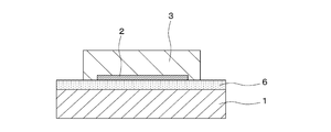
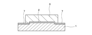
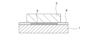
- thermoelectric conversion element of the thermoelectric power generation module which formed the easily bonding layer on the base material. It is sectional drawing which showed an example of the thermoelectric conversion element of the thermoelectric power generation module which used the base-material surface as the surface modification surface after forming an electrode on a base material. It is sectional drawing which showed an example of the thermoelectric conversion element of the thermoelectric power generation module which formed the electrode after making the base-material surface into a surface modification surface. It is sectional drawing which showed an example of the thermoelectric conversion element of the thermoelectric power generation module in which the conductive resin layer which coat
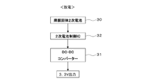
- FIG. It is the block diagram which showed a preferable example of the structure of the discharge of the thermoelectric power generation module demonstrated by embodiment. It is the top view which showed typically a preferable example of the electronic device carrying the thermoelectric power generation module which mounted the thin film solid secondary battery. It is sectional drawing which showed the base material used for the inkjet method. It is sectional drawing which showed the resistance measurement method, (a) is sectional drawing which showed the resistance value measurement between an electrode-thermoelectric conversion layer, (b) showed resistance value measurement between an electrode-thermoelectric conversion layer-wiring.
- FIG. It is the top view which showed the positional relationship of the electrode of Examples 21-23 and a thermal electrode conversion layer. It is the top view which showed the positional relationship of the electrode of Example 24 and a thermal electrode conversion layer. It is the top view which showed the positional relationship of the electrode of Example 25 and a thermal electrode conversion layer.
- thermoelectric power generation module of the present invention will be described in detail with reference to FIGS. Note that this description is not construed as being limited by the description of this embodiment.
- the thermoelectric power generation module 10 of the present embodiment includes a plurality of electrodes 2 on the main surface of a resin base material 1, and each electrode leaving a portion 2 a to which the wiring of the electrode 2 is connected.
- the thermoelectric conversion layer 3 made of resin that individually coats 2 is provided.
- the thermoelectric conversion layer 3 is bonded to the substrate 1 around the electrode 2 except for the surface of the electrode 2 and the portion 2a to which the wiring of the electrode 2 is connected.
- a wiring 4 for electrically connecting the thermoelectric conversion layer 3 and a portion (not shown) to which a wiring of another electrode adjacent to the electrode 2 (21) covered with the thermoelectric conversion layer 3 is connected is arranged.
- the wiring 4 is arranged so as not to be connected to the electrode 2 (21).
- the illustrated wiring 4 is narrower than the electrode 2 and the thermoelectric conversion layer 3, but may be equal to or wider than the width of the electrode 2 and the thermoelectric conversion layer 3.
- the thermoelectric conversion element 5 of the thermoelectric power generation module 10 is configured.
- thermoelectric conversion element 5 of the thermoelectric power generation module 10 is used with the wiring 4 side on the thermoelectric conversion layer 3 as a high temperature side and the electrode 2 side as a low temperature side, and the temperature between the wiring 4 and the electrode 2 is used. Electric energy is generated according to the difference. That is, in the thermoelectric conversion layer 3, a positive charge (hole) moves from the high-temperature wiring 4 side to the low-temperature electrode 2 side, thereby generating a potential difference and generating a thermoelectromotive force. The electromotive phenomenon is called the Seebeck effect.
- thermoelectric conversion layer 3 and the base material 1 if it is except a location except the part 2a to which the wiring of the electrode 2 is connected, there will be no limitation in particular in a shape or an area.
- the region of the substrate 1 in contact with the substrate may be used as a region to which the thermoelectric conversion layer 3 is bonded (hereinafter referred to as an adhesive portion), and the substrate in contact with any two sides or three sides from the viewpoint of improving the adhesive strength.
- thermoelectric conversion layer 3 is bonded to the base material 1 around the electrode 2 at least below the wiring 4 connected to the thermoelectric conversion layer 3.
- the adhesive portion By providing the adhesive portion in this manner, the adhesion between the thermoelectric conversion layer 3 and the substrate 1 becomes stronger.
- the region of the base material 1 that is in contact with the side of the electrode 2 on the side to which the wiring 4 is connected may be used as an adhesive portion.
- the width w of the bonding portion 3a is not particularly limited as long as there is no short circuit with the adjacent thermoelectric conversion layer, electrode, or wiring.
- the shape of the electrode 2 is a triangle, a polygon, a circle, a rounded square, or the like, the base material that is in contact with a side or a part of the side other than the part excluding the part 2a to which the wiring of the electrode 2 is connected. 1 region can be used as the bonding portion 3 a of the thermoelectric conversion layer 3.
- a rounded quadrangle is a quadrangle whose corner has a curvature.
- thermoelectric conversion layer 3 is bonded to the base material 1 below the wiring 4 connected to the thermoelectric conversion layer 3, a short circuit between the wiring 4 and the electrode 2 on the base material 1 can be prevented. In addition, recombination of electrons generated by the Seebeck effect in the wiring 4 and holes generated by the Seebeck effect in the thermoelectric conversion layer 3 can be suppressed, and an effect of increasing output power can be expected.
- the thermoelectric conversion layer 3 is bonded to the base material 1 around the electrode 2 at least below the wiring 4 connected to the thermoelectric conversion layer 3, and the width w of the bonding portion 3a is the thermoelectric conversion. It is preferably equal to or wider than the thickness t of the layer 3, and more preferably twice or more wider than the thickness t from the viewpoint of achieving both increased output voltage and adhesion.
- thermoelectric power generation device 20 of the thermoelectric power generation module 10 may be configured by arranging the thermoelectric conversion elements 5 vertically and horizontally on the base material 1 and electrically connecting them in series sequentially with the wiring 4. Good.
- each thermoelectric conversion element 5 is electrically connected in series in the form of a broken line.
- the number of arrangement of the thermoelectric conversion elements 5 shown in FIG. 3 is an example, and the number of arrangements of the thermoelectric conversion elements 5 depends on the electromotive force per thermoelectric conversion element 5 and the electromotive force as the thermoelectric conversion device 20.
- thermoelectric conversion elements 5 both ends of the thermoelectric conversion elements 5 connected in series become output terminals 51 and 52, and output wirings 53 and 54 are connected thereto.
- the electrode 2 of the thermoelectric conversion element 5, the wiring 4, or the electrode 23 connected to the wiring 4 can be used. Since the thermoelectric conversion elements 5 are connected in series in this way, current flows in one direction, the thermoelectromotive force generated in each thermoelectric conversion element 5 is added, and the desired electric energy is obtained by taking this out to the outside. It can generate electricity.
- the substrate 1 examples include a substrate such as a plastic film having flexibility.
- a plastic film is preferable because it is inexpensive and flexible.
- the base material 1 includes polyethylene terephthalate, polyethylene isophthalate, polyethylene naphthalate, polybutylene terephthalate, poly (1,4-cyclohexylenedimethylene terephthalate), polyethylene-2,6-phthalenedicarboxylate.
- Polyester resin such as polyimide, polycarbonate, polypropylene, polyethersulfone, cycloolefin polymer, polyetheretherketone (PEEK), triacetylcellulose (TAC), plastic film (resin film), glass epoxy, liquid crystalline polyester, Etc. are preferred.
- polyether ether ketone polyethylene terephthalate, polyethylene naphthalate, polyimide, glass epoxy, liquid crystalline polyester is preferable,
- polyethylene terephthalate, polyethylene naphthalate, polyimide, glass epoxy, and liquid crystalline polyester are preferable.
- a copolymer of the above resin or a blend of these resins with other types of resins can be used.
- inorganic or organic fine particles for example, inorganic fillers such as titanium oxide, calcium carbonate, silica, barium sulfate, silicone, etc., acrylic, benzoguanamine, Teflon ( (Registered trademark), an organic filler such as epoxy, polyethylene glycol (PEG), an adhesive improver such as sodium dodecylbenzenesulfonate, and an antistatic agent can be contained.
- inorganic fillers such as titanium oxide, calcium carbonate, silica, barium sulfate, silicone, etc., acrylic, benzoguanamine, Teflon (Registered trademark), an organic filler such as epoxy, polyethylene glycol (PEG), an adhesive improver such as sodium dodecylbenzenesulfonate, and an antistatic agent can be contained.
- inorganic fillers such as titanium oxide, calcium carbonate, silica, barium sulfate, silicone, etc., acrylic, benzoguanamine, Teflon (Registered trademark),
- each resin film can be selected from known methods and conditions as appropriate.
- a polyester film can be formed by melt-extrusion of a polyester resin into a film, orientation crystallization by longitudinal and transverse biaxial stretching, and crystallization by heat treatment.
- the thickness of the resin film used as a base material is 5 ⁇ m or more and 1000 ⁇ m or less, and from the viewpoint of flexibility, the thickness is 10 ⁇ m or more and 500 ⁇ m or less. It is preferable to use those of 10 ⁇ m or more and 250 ⁇ m or less.
- the substrate 1 preferably further contains an additive such as an ultraviolet absorber from the viewpoint of preventing deterioration of the substrate.
- an ultraviolet absorber an oxazole, triazine, stilbene, or coumarin absorber can be suitably used.
- any of known materials such as metal electrodes such as copper, silver, gold, platinum, nickel, chromium, and copper alloys, and transparent electrodes such as indium tin oxide (ITO) and zinc oxide (ZnO) are used.
- metal electrodes such as copper, silver, gold, platinum, nickel, chromium, and copper alloys
- transparent electrodes such as indium tin oxide (ITO) and zinc oxide (ZnO)
- ITO indium tin oxide
- ZnO zinc oxide
- any of copper, gold, platinum, nickel, copper alloy, etc. is used, and more preferably, any of gold, platinum, nickel is used.
- the thermoelectric conversion layer 3 includes a carbon nanotube (hereinafter also referred to as CNT) and a resin layer serving as a binder.
- the resin layer serving as a binder include vinyl compounds, (meth) acrylate compounds, carbonate compounds, and ester compounds.
- the vinyl compound include polystyrene, polyvinyl naphthalene, polyvinyl acetate, polyvinyl phenol, polyvinyl butyral, and the like.
- the (meth) acrylate compound include polymethyl (meth) acrylate, polyethyl (meth) acrylate, polyphenoxy (poly) ethylene glycol (meth) acrylate, polybenzyl (meth) acrylate, and the like.
- Examples of the carbonate compound include bisphenol Z-type polycarbonate and bisphenol C-type polycarbonate.
- Examples of the ester compound include amorphous polyester.
- Preferred examples include polyvinyl butyral, (meth) acrylate compounds, carbonate compounds, and ester compounds, and more preferred are polyvinyl butyral, polyphenoxy (poly) ethylene glycol (meth) acrylate, polybenzyl (meth) acrylate, and amorphous polyester. Is mentioned.
- nanocarbons such as carbon nanohorns, carbon nanocoils, carbon nanobeads, graphite, graphene, and amorphous carbon may be included.
- the wiring 4 may be formed using either a conductive paste in which conductive fine particles such as silver and carbon are dispersed or a conductive paste containing metal nanowires such as silver, copper and aluminum. it can.
- a conductive paste in which conductive fine particles such as silver and carbon are dispersed
- a conductive paste containing metal nanowires such as silver, copper and aluminum.
- conductive paste By using conductive paste, it is possible to follow the step between the upper surface of the thermoelectric conversion layer and the electrode on the substrate, connect without disconnection or contact failure, high output power, and reliability A highly functional module can be formed.
- known conductive materials such as metals such as gold, silver, copper and nickel, alloy materials thereof, and oxide semiconductor materials such as indium tin oxide (ITO) Therefore, wiring may be performed.
- thermoelectric power generation module 10 having the thermoelectric power generation device 20
- the resin thermoelectric conversion layer 3 is bonded to the resin base material 1 around the electrode 2 except for the portion where the wiring of the electrode 2 is connected.
- a stronger adhesive force than that on the electrode 2 made of metal can be obtained.
- the flexibility of the thermoelectric power generation module 10 can be improved, and the thermoelectric power generation module 10 strong against bending can be provided.
- thermoelectric power generation module 10 since the thermoelectric power generation module 10 has the resin thermoelectric conversion layer 3 on the resin substrate 1, it is excellent in flexibility. In particular, since a part of the thermoelectric conversion layer 3 is adhered to the base material 1 so as to protrude from the electrode 2 to the base material 1 side, the adhesion between the base material 1 and the thermoelectric conversion layer 3 is strengthened. Yes. Therefore, even when the substrate 1 is bent, the thermoelectric conversion layer 3 is difficult to peel off from the electrode 2. As a result, durability against bending can be obtained, and it can withstand repeated use. Moreover, since the said thermoelectric conversion layer 3 is resin, it can produce by application
- the easy-adhesion layer 6 which raises the adhesiveness of the surface on the base material 1.
- the easily adhesive layer 6 is used as an adhesive layer
- the electrode 2 is disposed on the surface thereof
- the thermoelectric conversion layer 3 is disposed around the electrode 2 except for the portion to which the wiring of the electrode 2 is connected (see FIG. 1). It adheres to the easy adhesion layer 6.
- Examples of the easy adhesion layer 6 include gelatin, polyvinyl alcohol (PVA), acrylic resin, urethane resin, and polyester resin.
- PVA polyvinyl alcohol
- acrylic resin, urethane resin, and polyester resin are used.
- crosslinking agents such as a carbodiimide crosslinking agent, an isocyanate crosslinking agent, and a melamine crosslinking agent.
- thermoelectric conversion layer 3 By forming the easy adhesion layer 6, the adhesive force of the thermoelectric conversion layer 3 can be further increased.
- the surface modification layer 7 is formed.
- the surface modification layer which has the surface modification surface obtained by irradiating the surface of the base material 1 with an energy ray 7 is preferably formed. Therefore, it is preferable that the surface modification layer 7 is formed on the surface of the base material 1 at least as a base surface of the thermoelectric conversion layer 3.
- corona treatment using corona discharge corona treatment using corona discharge
- plasma treatment for exposure to plasma atmosphere UV ozone treatment for ultraviolet irradiation in ozone atmosphere
- EB irradiation treatment for irradiating electron beam etc.
- plasma treatment, corona treatment, and UV ozone treatment are preferable.
- a polar hydroxyl group, carboxyl group, basic group or the like can be generated on the surface of the base material, and the adhesiveness with the thermoelectric conversion layer 3 is further improved.
- the surface modification surface is obtained by roughening the surface of the base material 1 by irradiation of energy rays, and the adhesion area between the base material 1 and the thermoelectric conversion layer 3 is increased by increasing the surface area, thereby increasing the adhesive force. Also good.
- the surface modification layer 7 may be formed on the surface of the easy-adhesion layer 6 (see FIG. 4) or the conductive resin layer described later. Thereby, the adhesive force between the surface of the easy-adhesion layer 6 or the surface of the conductive resin layer and the thermoelectric conversion layer 3 which is the base surface of the thermoelectric conversion layer 3 can be further increased.
- the adhesion of the metal wiring layer and the protective layer can also be improved.
- a water-soluble resin such as polyvinyl alcohol (PVA) or polyvinyl pyrrolidone (PVP) having a high oxygen barrier property can be applied as a protective layer.
- PVA polyvinyl alcohol
- PVP polyvinyl pyrrolidone
- the conductive resin layer 8 is provided on the base material 1 and the electrode 2, the thermoelectric conversion layer 3 is disposed on the conductive resin layer 8, and the thermoelectric conversion layer 3 is connected to the electrode 2. It is preferable to adhere to the conductive resin layer 8 above and around the electrode 2 except for the portion to which the upper wiring is connected (see FIG. 1). In this configuration, the conductivity of the thermoelectric conversion layer 3 is made higher than that of the conductive resin layer 8. In the configuration having the conductive resin layer 8, since the electrode 2 is covered with the conductive resin layer 8 and the thermoelectric conversion layer 3 is disposed on the conductive resin layer 8, the adhesiveness to the thermoelectric conversion layer 3 is poor.
- Examples of the conductive resin layer 8 include PEDOT / PSS, PEDOT / Nafion (registered trademark), PEDOT / PVS, and the like, and preferably PEDOT / PSS.
- PEDOT is an abbreviation for poly (3,4-ethylenedioxythiophene)
- PSS is an abbreviation for poly-4 styrene sulfonate
- PVS is an abbreviation for polyvinyl sulfonic acid.
- Nafion is a perfluorocarbon material having a sulfonic acid group.
- thermoelectric power generation module 10 in which the thin film solid secondary battery electrically connected to the output portion of the thermoelectric conversion layer 3 is mounted will be described with reference to FIGS. 8 and 9. To do.
- thermoelectric power generation module 10 Since the electric power generated in the thermoelectric power generation module 10 is direct current power and has a low voltage, it is difficult to use the electric power as it is for driving an electronic device or the like. Therefore, the voltage obtained by the thermoelectric power generation module 10 is boosted by the DC-DC converter 31. For example, the voltage is boosted to 4.0V. Subsequently, the thin-film solid secondary battery as the secondary battery 30 is charged with the boosted voltage via the secondary battery control IC 32 that controls charging and discharging of the secondary battery 30.
- the secondary battery control IC 32 includes a power supply device that generates DC power for charging and a charge control circuit that controls charging of the battery.
- the voltage discharged from the thin-film solid secondary battery as the secondary battery 30 via the secondary battery control IC 32 is sent to the DC-DC converter 31, and the voltage used by the DC-DC converter 31 in the electronic device (not shown). Convert to and output.
- the operating voltage of an electronic device is various voltages. Therefore, the DC-DC converter 31 steps down or boosts the voltage used by the electronic device. For example, the voltage is transformed to 3.3V and output.
- DC-DC converter 31 for example, ETC310 manufactured by En Ocean, LTC3108, LTC3109 manufactured by Linear Technology, or the like can be used.
- secondary battery control IC 32 for example, LTC4070, LTC4071 manufactured by Linear Technology, MAX17710 manufactured by Maxim Integrated Products, or the like can be used.
- MEC201, MEC220 manufactured by Infinite Power Solution can be used for example.
- thermoelectric power generation module 10 includes a thermoelectric power generation device 20, a secondary battery 30 (for example, a thin film solid secondary battery), and an electronic device 40 on a flexible substrate 11, a secondary battery control IC 32 (FIG. 8 and 9)) and the like are connected.
- a secondary battery 30 for example, a thin film solid secondary battery
- an electronic device 40 on a flexible substrate 11 a secondary battery control IC 32 (FIG. 8 and 9)
- As the cable 34 an FPC (flexible printed circuit) cable or an FFC (flexible flat cable) is used.
- the thermoelectric power generation module 10 is attached to the heat generation source 50.
- the secondary battery 30 may be mounted on the thermoelectric generator 20.
- thermoelectric power generation module 10 can be suitably used for applications such as the power supply for electronic devices.
- thermoelectric power generation module 10 may be formed by bonding the thermoelectric conversion layer 3 to the base material 1 so as to protrude from the electrode 2 in a known manufacturing method of a thermoelectric power generation module.
- the electrode 2 can be formed by a plating method, a patterning method by etching, a sputtering method using a lift-off method, an ion plating method, a sputtering method using a metal mask, an ion plating method, or the like.
- a metal paste in which the above-described metal is finely divided and a binder and a solvent are added may be used.
- a screen printing method or a printing method using a dispenser method can be used. After printing, heating for drying and heat treatment for decomposition of the binder and sintering of the metal may be performed.
- the thermoelectric conversion layer 3 is a metal mask printing method using a metal mask to print a carbon nanotube dispersed paste, an ink jet printing method in which an ink jet coating liquid containing carbon nanotubes is ejected by an ink jet method, printing such as screen printing. It is preferable to carry out by a method or the like.
- the screen printing method involves patterning exposure of a photosensitive resin onto a normal mesh made of stainless steel, nylon, or polyester, developing it to produce a plate, printing, and printing a plate from an etched metal mask. And printing methods.
- the metal mask printing method will be described in detail later in Examples.
- the inkjet printing method is performed as follows.
- the total solid content concentration in the coating liquid for inkjet is generally 0.05% by mass or more and 30% by mass or less, more preferably 0.1% by mass or more and 20% by mass or less, and further preferably 0.1% by mass. It is 10 mass% or less.
- the viscosity in the coating solution is generally from 1 mPa ⁇ s to 30 mPa ⁇ s, more preferably from 1.5 mPa ⁇ s to 20 mPa ⁇ s, and even more preferably from 1.5 mPa ⁇ s, from the viewpoint of ejection stability. This is 15 mPa ⁇ s or less.
- This coating solution is used by dissolving and dispersing the above-described components in a predetermined organic solvent, filtering the solution, and applying the solution on a predetermined support or layer as follows.
- the pore size of the filter used for filter filtration is preferably 2.0 ⁇ m or less, more preferably 0.5 ⁇ m or less made of polytetrafluoroethylene, polyethylene or nylon.
- the solvent (coating solvent) that dissolves or compatibilizes the organic substance that is the thermoelectric material and the solvent that disperses the nano conductive material are appropriately selected according to the organic substance or the nano conductive material that is the thermoelectric material.
- Conventionally known solvents can be used.
- the solvent include known organic solvents such as aromatic hydrocarbon solvents, alcohol solvents, ketone solvents, aliphatic hydrocarbon solvents, amide solvents, and halogenated solvents.
- aromatic hydrocarbon solvent examples include benzene, toluene, xylene, trimethylbenzene, tetramethylbenzene, cumene, ethylbenzene, methylpropylbenzene, methylisopropylbenzene, tetrahydronaphthalene, and the like, and xylene, cumene, trimethylbenzene, tetra Methylbenzene and tetrahydronaphthalene are more preferable.
- Examples of the alcohol solvent include methanol, ethanol, butanol, benzyl alcohol, cyclohexanol and the like, and benzyl alcohol and cyclohexanol are more preferable.
- ketone solvents include 1-octanone, 2-octanone, 1-nonanone, 2-nonanone, acetone, 4-heptanone, 1-hexanone, 2-hexanone, 2-butanone, diisobutylketone, cyclohexanone, methylcyclohexanone, phenylacetone, Examples thereof include methyl ethyl ketone, methyl isobutyl ketone, acetyl acetone, acetonyl acetone, ionone, diacetonyl alcohol, acetyl carbinol, acetophenone, methyl naphthyl ketone, isophorone, propylene carbonate and the like, and methyl isobutyl ketone and propylene carbonate are preferable.
- Examples of the aliphatic hydrocarbon solvent include pentane, hexane, octane and decane, and octane and decane are preferable.
- amide solvents include N-methyl-2-pyrrolidone, N-ethyl-2-pyrrolidone, N, N-dimethylacetamide, N, N-dimethylformamide, 1,3-dimethyl-2-imidazolidinone and the like. N-methyl-2-pyrrolidone and 1,3-dimethyl-2-imidazolidinone are preferred.
- halogenated solvent examples include chloroform, chlorobenzene, dichlorobenzene and the like, and chlorobenzene and dichlorobenzene are preferable.
- the said solvent may be used independently and may use 2 or more types together.
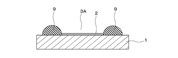
- thermoelectric conversion layer As shown in FIG. 11, it is preferable to use the base material 1 used in the ink jet printing method in which the bank 9 is formed so as to surround the outer periphery of the region 3a where the thermoelectric conversion layer is formed. That is, the region 3 a for forming the thermoelectric conversion layer is all partitioned by the bank 9. For this reason, the coating liquid containing the thermoelectric conversion material deposited by the ink jet method by the bank 9 can be retained in the bank 9, and a thermoelectric conversion layer (not shown) having a height can be formed.
- the cross-sectional shape of the bank 9 examples include an arc shape (semi-circle, semi-ellipse), a triangle, a parabola shape, a trapezoid, and the like.
- the upper portion of the bank 9 preferably does not have a flat portion. Therefore, the cross-sectional shape of the bank 9 is preferably a convex curved surface shape such as a semicircular shape, a semielliptical shape, a triangular shape, or a parabolic shape.
- the bank 9 is more preferably an arc shape or a triangle, and more preferably an arc shape.
- Examples of the material of the bank 9 include polyimide, novolac resin, epoxy resin, acrylic resin, and the like, and polyimide is preferable from the viewpoint of liquid repellency and heat resistance.
- the bank may be subjected to a liquid repellent treatment as necessary.
- a fluorocarbon film may be formed on the bank 9 by chemical vapor deposition (CVD) using carbon tetrafluoride (CF 4 ) as a source gas, and a long-chain fluoroalkyl group may be used.
- CVD chemical vapor deposition
- CF 4 carbon tetrafluoride
- a silane coupling agent having fluorine or a fluoropolymer may be mixed in the bank.
- the bank 9 can be formed by using a photosensitive resist including dry resist, polyimide, a method using patterning and developing with UV light using photosensitive glass, a resist is laminated on a polyimide capable of alkali development, and UV light is applied. And a method using patterning and development by UV, and a method using patterning by screen printing using an epoxy resin and UV crosslinking.
- the region 3a where the thermoelectric conversion layer is formed is a region surrounded by the bank 9, and a coating liquid containing an organic substance as a thermoelectric material and a nano conductive material is applied to the region 3a. If necessary, the layer may be formed by applying a coating liquid containing other organic substances before and after the coating liquid is applied to the region 3a where the thermoelectric conversion layer is formed.
- the heating temperature and time after coating are not particularly limited as long as the coating solution dries, but the heating temperature is generally 100 ° C. or higher and 200 ° C. or lower, and preferably 120 ° C. or higher and 160 ° C. or lower.
- the heating time is generally from 1 minute to 120 minutes, preferably from 1 minute to 60 minutes, and more preferably from 1 minute to 25 minutes.
- any method such as a method of drying in a low-pressure atmosphere using a vacuum pump or the like, a method of drying while blowing air using a fan, or a method of drying while supplying an inert gas (nitrogen, argon) is used. Can be used.
- the thermoelectric conversion layer may be formed thick by repeating inkjet printing and heat drying a plurality of times. In addition, about heat drying, it does not matter whether the solvent component completely volatilizes or not.
- thermoelectric conversion element of Example 1 was produced as follows. ⁇ Preparation of carbon nanotube paste 1> 3 g of silica fine particles JA-244 (manufactured by Jujo Chemical) was added to 27 g of polystyrene having a polymerization degree of 2000 (manufactured by Kanto Chemical Co., Ltd.), and dispersed with a two-roll mill heated to 180 ° C. to prepare silica-dispersed polystyrene.
- ultrasonic homogenizer VC-750 (trade name) manufactured by Inc. and a taper microtip (probe diameter 6.5 mm)
- ultrasonic dispersion is performed at 30 ° C. for 30 minutes at an output of 50 W, direct irradiation, and a duty ratio of 50%.
- a carbon nanotube dispersion was prepared.
- silica-dispersed polystyrene prepared with 1.0 g of PC-Z type polycarbonate (manufactured by Teijin Chemicals Ltd., Panlite TS-2020 (trade name)) as a non-conjugated polymer was added, After dissolving in a warm bath, the carbon nanotube dispersion paste 1 was prepared by stirring with a revolutionary stirring device ARE-250 (trade name) manufactured by Shinky Co., Ltd. with a rotation speed of 2200 rpm and a stirring time of 15 minutes.
- ARE-250 trade name
- a base material of a polyethylene terephthalate (PET) film was formed by the following procedure. First, a PET resin having an intrinsic viscosity of 0.66 polycondensed using germanium (Ge) as a catalyst was dried to a moisture content of 50 ppm or less, a heater temperature was set to 280 ° C. or more and 300 ° C. or less, and the mixture was melted in an extruder. The melted PET resin was discharged from a die part onto a chill roll electrostatically applied to obtain an amorphous base. The obtained amorphous base was stretched 3.3 times in the base traveling direction and then stretched 3.8 times in the width direction to obtain a PET film substrate having a thickness of 188 ⁇ m.
- germanium germanium
- thermoelectric conversion element An electrode was formed on an A6 size PET film by laminating 100 nm of chromium and then 200 nm of gold by ion plating using a 6 ⁇ 9 mm opening metal mask formed by etching. Next, using the metal mask having 80 openings 8 ⁇ 9 mm formed by laser processing and having a thickness of 2 mm, the carbon nanotube dispersion paste prepared above was injected and flattened with a squeegee. At this time, the carbon nanotube dispersion paste 1 was printed on the electrode 2 in the arrangement as shown in FIG. The thermoelectric conversion element was formed on the electrode by heating and drying the PET film on an 80 ° C. hot plate.
- thermoelectric conversion element of Example 2 was produced as follows. ⁇ Formation of easy adhesion layer> A PET film substrate having a thickness of 188 ⁇ m produced by the same method as in Example 1 was conveyed at a conveyance speed of 80 m / min, and after corona discharge treatment was performed on both surfaces under the condition of 730 J / m 2 , A coating solution for an easy-adhesion layer having the following formulation was applied by a bar coating method at a coating amount of 4.4 cm 3 / m 2 on both surfaces. And this was dried at 160 degreeC for 1 minute, and the PET film by which the easy-adhesion layer was apply-formed on both surfaces of the base material was obtained by forming an easy-adhesion layer.
- thermoelectric conversion element was produced in the same manner as in Example 1 except that instead of the PET film on which the easy adhesion layer was formed, a PET film on which the easy adhesion layer was applied and formed on both surfaces of the base material was used.
- thermoelectric conversion element of Example 3 was produced as follows. Using a metal mask having an opening of 6 ⁇ 9 mm formed by etching on a base material of a 188 ⁇ m-thick PET film produced by the same method as in Example 1, 100 nm of chromium is then deposited by ion plating and then gold An electrode was formed by forming a 200 nm thick film.
- thermoelectric conversion element was produced in the same manner as in Example 1.
- thermoelectric conversion element of Example 4 was produced as follows.
- a 125 ⁇ m-thick polyimide film Kapton 500V (manufactured by Toray DuPont) is used, and instead of the atmospheric pressure plasma surface device, a UV ozone device: UVO Cleaner 42 (Jeight Company, Inc. trade name) is used, A thermoelectric conversion element was produced in the same manner as in Example 3 except that UV ozone treatment was performed for 10 minutes.
- thermoelectric conversion element of Example 5 was produced as follows.
- a base material a PET film coated with an easy-adhesion layer prepared by the method of Example 1 was used, and a corona surface modification device TEC-4AX (manufactured by Kasuga Denki) was used instead of the atmospheric pressure plasma surface device.
- a thermoelectric conversion element was produced in the same manner as in Example 3 except that the surface modification treatment was performed with an electrode output of 80 W, an electrode moving speed of 1 m / min, and a frequency of 2 times.
- thermoelectric conversion element of Example 6 was produced as follows. ⁇ Preparation> As a conductive resin layer (undercoat layer), 90 parts by mass of PEDOT / PSS dispersion: CLEVIOS P VP8000 (product name of Heraeus) and 10 parts by mass of isopropyl alcohol (manufactured by Kanto Chemical Co., Inc.) are mixed, and a mixed rotor: MR-3 (Manufactured by ASONE) was stirred for 1 hour. After stirring, filtration was performed with a PVDF mesh having a mesh opening of 70 ⁇ m to prepare a PEDOT / PSS dispersion.
- ⁇ Preparation of base material> Using a metal mask having an opening of 6 ⁇ 9 mm formed by etching on a PET film substrate on which an easy-adhesion layer produced by the same method as in Example 1 was applied, chromium was 100 nm by ion plating, Next, an electrode was formed by depositing gold in a thickness of 200 nm. Next, automatic coating apparatus: PI-1210 (manufactured by Tester Sangyo) and bar coater ROD No. 4 was applied on the base material on which the electrode was formed under the condition of a coating speed of 50 mm / sec. After coating, the substrate was dried on a hot plate at 80 ° C. for 5 minutes, and then dried for 1 hour in a vacuum dryer having an atmospheric pressure of 0.2 kPa or less and an internal temperature of 80 ° C., and a conductive resin layer as an undercoat layer was formed. A PET film substrate was prepared.
- thermoelectric conversion element was produced in the same manner as in Example 1 except that a PET film substrate on which a conductive resin layer was formed was used as the substrate.
- thermoelectric conversion element of Example 7 was produced as follows. A thermoelectric conversion element was produced in the same manner as in Example 1 except that PEN film Teonex Q51DW (trade name of Teijin DuPont) on which an easy-adhesion layer having a thickness of 50 ⁇ m was applied and formed was used.
- PEN film Teonex Q51DW trade name of Teijin DuPont
- thermoelectric conversion element of Example 8 was produced as follows. ⁇ Preparation of base material> As a base material, a 125 ⁇ m-thick polyimide: Kapton 500V (manufactured by Toray DuPont) is used, a wet blasting device WFB-2-2 (manufactured by Macau) is used, an alumina grinding stone (particle size 800), 0.7 kg / m as an abrasive. Blasting was performed at a water pressure of 2 and a processing speed of 10 m / min to produce a roughened polyimide substrate.
- Kapton 500V manufactured by Toray DuPont
- WFB-2-2 wet blasting device
- alumina grinding stone particle size 800
- Blasting was performed at a water pressure of 2 and a processing speed of 10 m / min to produce a roughened polyimide substrate.
- thermoelectric conversion element was produced in the same manner as in Example 1 except that a roughened polyimide base material was used as the base material.
- thermoelectric conversion element of Example 9 was produced as follows. Using a metal mask having an opening of 6 ⁇ 9 mm formed by etching on a base material of a 188 ⁇ m-thick PET film produced by the same method as in Example 1-1, chromium was deposited to 100 nm by the ion plating method. An electrode was formed by depositing a gold film with a thickness of 200 nm. Thereafter, a thermoelectric conversion element was formed in the same manner as in Example 1.
- thermoelectric conversion element of Example 10 was produced as follows. Using a metal mask with an opening 6 ⁇ 9 mm formed by etching on a 125 ⁇ m-thick polyimide: Kapton 500V (manufactured by Toray DuPont) as a base material, chromium is 100 nm by an ion plating method, and then gold is 200 nm. An electrode was formed by laminating. Thereafter, a thermoelectric conversion element was formed in the same manner as in Example 1.
- Kapton 500V manufactured by Toray DuPont
- thermoelectric conversion element of Example 11 was produced as follows.
- the base material, easy-adhesion layer, and thermoelectric conversion element were produced in the same manner as in Example 1 except that the carbon nanotube dispersion paste 2 was used instead of the carbon nanotube dispersion paste 1.
- ⁇ Production of carbon nanotube paste 2> Poly (1-vinylnaphthalene) (Aldrich, 191165 (product code)) instead of PC-Z type polycarbonate (Teijin Chemicals, Panlite TS-2020 (trade name)) is used as a non-conjugated polymer.
- a carbon nanotube-dispersed paste 2 was prepared according to the same method as in Preparation 1 of carbon nanotube paste except that it was used.
- Example 12 The thermoelectric conversion element of Example 12 was produced as follows.
- the base material, easy-adhesion layer, and thermoelectric conversion element were prepared in the same manner as in Example 1 except that the carbon nanotube dispersion paste 3 was used instead of the carbon nanotube dispersion paste 1.
- ⁇ Production of carbon nanotube paste 3> Other than using polymethyl methacrylate (Aldrich, 200035 (product code)) instead of PC-Z type polycarbonate (Teijin Chemicals, Panlite TS-2020 (trade name)) as a non-conjugated polymer
- a carbon nanotube dispersion paste 3 was prepared according to the same method as in preparation 1 of carbon nanotube paste.
- thermoelectric conversion element of Example 21 was produced as follows.
- the base material, easy-adhesion layer and thermoelectric conversion element were prepared in the same manner as in Example 1 except that the carbon nanotube dispersion paste 4 was used instead of the carbon nanotube dispersion paste 1.
- ⁇ Production of carbon nanotube paste 4> In addition to using PC-Z type polycarbonate (Teijin Kasei Co., Ltd., Panlite TS-2020 (trade name)) as a non-conjugated polymer, benzyl methacrylate polymer (Aldrich, 181350 (product code) was used. Produced a carbon nanotube dispersion paste 4 according to the same method as in Production 1 of carbon nanotube paste.
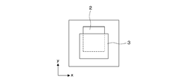
- thermoelectric conversion element An electrode was formed on an A6 size PET film by laminating 100 nm of chromium and then 200 nm of gold by ion plating using a 6 ⁇ 9 mm opening metal mask formed by etching. Next, using the metal mask having 80 openings 8 ⁇ 9 mm formed by laser processing and having a thickness of 2 mm, the carbon nanotube dispersion paste 4 prepared above was injected and flattened with a squeegee. At this time, the carbon nanotube dispersion paste 4 was printed on the electrode 2 in the arrangement as shown in FIG. The thermoelectric conversion element was formed on the electrode by heating and drying the PET film on an 80 ° C. hot plate. At this time, as shown in FIG. 13, the thermoelectric conversion layer 3 was printed so that the three sides around the electrode 2 protrude in both the one direction of the y direction and the x direction.
- thermoelectric power generation module 80 thermoelectric conversion elements were connected in series by applying silver paste: FA-333 (manufactured by Fujikura Kasei), and dried on a hot plate at 80 ° C. for 1 hour to produce the thermoelectric power generation module 10.
- 70 g of polyvinylpyrrolidone K-30 (manufactured by Tokyo Chemical Industry) is dissolved in 96 g of a mixed solvent of pure water / isopropyl alcohol (volume ratio 80:20) and filtered through a PVDF mesh having a mesh opening of 70 ⁇ m.
- a polymer solution for overcoat was prepared.
- thermoelectric power generation module 10 was produced.
- Example 22 Except for having 80 openings 8 ⁇ 7.7 mm formed by laser processing and using a metal mask having a thickness of 2 mm, the carbon nanotube dispersion paste 4 prepared above was injected and flattened with a squeegee, A thermoelectric power generation module 10 of Example 22 was produced in the same manner as in Example 21. At this time, as shown in FIG. 13, the thermoelectric conversion layer 3 was printed so that the three sides around the electrode 2 protrude in both the one direction of the y direction and the x direction.
- Example 23 Except for injecting the carbon nanotube dispersion pace 4 prepared above using a metal mask having 80 openings 8 ⁇ 8 mm formed by laser processing and having a thickness of 2 mm, and flattening with a squeegee.
- the thermoelectric power generation module 10 of Example 23 was produced by the same method as in Example 21. At this time, as shown in FIG. 13, the thermoelectric conversion layer 3 was printed so that the three sides around the electrode 2 protrude in both the one direction of the y direction and the x direction.
- Example 24 Except for injecting the carbon nanotube dispersion paste 4 prepared above using a metal mask having 80 openings 6 ⁇ 9 mm formed by laser processing and having a thickness of 2 mm, and flattening with a squeegee.
- the thermoelectric power generation module 10 of Example 24 was produced in the same manner as in Example 21. At this time, as shown in FIG. 14, the thermoelectric conversion layer 3 was printed such that one side around the electrode 2 protruded only in one direction in the y direction.
- Example 25 Except for having 80 openings 8 ⁇ 7.5 mm formed by laser processing and using a metal mask with a thickness of 2 mm, the carbon nanotube dispersion paste 4 prepared above was injected and flattened with a squeegee, A thermoelectric power generation module 10 of Example 25 was produced in the same manner as in Example 21. At this time, as shown in FIG. 15, the thermoelectric conversion layer 3 was printed so that two sides around the electrode 2 protrude in both directions in the x direction.
- thermoelectric conversion element of Comparative Example 1 was produced as follows. ⁇ Production of thermoelectric conversion element> Using a metal mask having an opening of 6 ⁇ 9 mm formed by etching on a PET film substrate produced by the same method as in Example 1, 100 nm of chromium and 200 nm of gold were laminated by ion plating. By forming a film, an electrode was formed. Next, using a metal mask having 80 openings 8 ⁇ 7.5 mm formed by laser processing and having a thickness of 2 mm on a PET film with electrodes, without any particular surface treatment. The carbon nanotube dispersion paste was injected and flattened with a squeegee. At this time, the carbon nanotube dispersion paste was printed only on the electrode. The substrate was heated and dried on a hot plate at 80 ° C. to produce a thermoelectric conversion element.
- thermoelectric conversion element of Comparative Example 2 was produced as follows. A thermoelectric conversion element was prepared in the same manner as in Comparative Example 1 except that a surface treatment was performed on a PET film with electrodes using a UV ozone apparatus: UVO Cleaner 42 (trade name of Jeight Company, Inc.) with an irradiation time of 10 minutes. Produced.
- thermoelectric conversion element of Comparative Example 3 was produced as follows. Using a metal mask having an opening of 6 ⁇ 9 mm formed by etching on the PET film substrate on which the easy-adhesion layer prepared in Example 1 was applied and formed, 100 nm of chromium and then gold by ion plating were used. An electrode was formed by forming a 200 nm stacked film. Next, using a metal mask having 80 openings 8 ⁇ 7.5 mm formed by laser processing and having a thickness of 2 mm on a PET film with electrodes, without any particular surface treatment. The carbon nanotube dispersion paste was injected and flattened with a squeegee. At this time, the carbon nanotube dispersion paste was printed only on the electrode. The substrate was heated and dried on a hot plate at 80 ° C. to produce a thermoelectric conversion element.
- thermoelectric power generation module of Comparative Example 21 was produced in the same manner as in Example 21. At this time, the thermoelectric conversion layer was printed without protruding around the electrode.
- thermoelectric conversion element evaluation of thermoelectric conversion element
- ⁇ Tape peeling test> Cellotape (registered trademark) (width: 12 mm) CT-12 (manufactured by Nichiban) was attached to the formed thermoelectric conversion layer.
- CT-12 manufactured by Nichiban
- thermoelectric conversion layer The case where there is no peeling of the thermoelectric conversion layer is represented by “A” as excellent peeling resistance, Although there is peeling in a part of the thermoelectric conversion layer, the peeling resistance is represented by “C” as being practically usable, The case where the thermoelectric conversion layer completely peeled was represented by “D” because the peel resistance was inferior.
- thermoelectric power generation layers are coated with silver paste: FA-333 (manufactured by Fujikura Kasei) and dried on an 80 ° C. hot plate for 1 hour to form wiring and connect ten thermoelectric power generation modules. Produced. The resistance value of each line was measured with a tester, and the ratio of the resistance values before and after the heating and bending resistance tests was calculated. Furthermore, the presence or absence of peeling was confirmed visually.
- a 60 W incandescent bulb was lit at the center of an ABS resin pipe having an outer diameter of 35 mm and an inner diameter of 25 mm. At this time, the ambient temperature was 25 ° C., and the temperature of the pipe surface was 45 ° C. The process of winding a thermoelectric power generation module around this pipe and holding it for 3 minutes was repeated 5 times, and then resistance value measurement and visual evaluation were performed. Further, the resistance change rate and the increase rate were average values of 10 lines.
- Resistance change rate (increase rate) ⁇ (Resistance value after resistance test) ⁇ (resistance value before test) ⁇ / (resistance value before resistance test) ⁇ 100
- the rate of change in resistance was determined according to the following criteria.
- the resistance change rate is within ⁇ 2%, and the case where there is no peeling of the thermoelectric conversion layer is represented by “A” as being excellent in heating and bending resistance,
- the resistance change rate is 2% or more and less than 10%, and the case where there is no peeling of the thermoelectric conversion layer is represented by “B” as good heating and bending resistance,
- the resistance change rate is 10% or more, and cracks occurred in the thermoelectric conversion layer, but the heating and bending resistance is represented by “C” as practically usable, Resistance measurement is not possible, and the case where peeling occurs in the thermoelectric conversion layer is represented by “D” as inferior in heating and bending resistance.
- Resistance change rate ⁇ (resistance value A) ⁇ (resistance value B) ⁇ / (resistance value A) ⁇ 100
- thermoelectric generator module Evaluation of thermoelectric generator module The following evaluation was performed about the produced thermoelectric power generation module.
- thermoelectric conversion layer ⁇ Measurement of protrusion width of thermoelectric conversion layer>
- the back surface of the PET is observed and measured with a measuring microscope MM400 / LU (manufactured by Nikon Co., Ltd.), and the shortest length from the end of the electrode to the end of the thermoelectric conversion layer is defined as the width of the thermoelectric conversion layer protruding around the electrode portion. did.
- thermoelectric conversion layer Using a laser microscope VK-X200 (manufactured by Keyence Corporation), the height from the gold electrode to the top of the thermoelectric conversion layer was measured, and the measured value was taken as the thickness of the thermoelectric conversion layer.
- thermoelectric voltage of thermoelectric generator module A thermoelectric generator module was placed on a water-cooled heat sink P-200S (manufactured by Takagi Seisakusho Co., Ltd.) so that the PET substrate and stainless steel were in contact with each other. Next, a heater plate HU-600C (manufactured by Takagi Seisakusho Co., Ltd.) was placed in contact with the thermoelectric conversion layer.
- the temperature of the water-cooled heat sink is adjusted so that the PET substrate temperature becomes 20 ° C. and the heater plate is maintained at 50 ° C.
- the voltage generated at both ends of 80 thermoelectric conversion elements connected in series is digital multimeter R6871E. (Measured by Advantest Co., Ltd.), and the measured value was used as the thermoelectromotive force of the thermoelectric power generation module.
- Tables 1 to 4 show the evaluation results of the thermoelectric conversion elements, and Table 5 shows the evaluation results of the thermoelectric power generation module.
- thermoelectric conversion layer has improved adhesion to the substrate according to the present invention and exhibits good performance in the tape peeling test and the heating and bending resistance test.
- the adhesiveness of the thermoelectric conversion layer is improved by maintaining the wettability improved by the easy-adhesion layer.
- the UV ozone treatment of the polyimide substrate with the surface treatment, the imide ring is opened, the wettability is maintained, and the base material has a low coefficient of thermal expansion. It can be said that it showed heating and bending resistance.
- thermoelectric conversion layer protrudes from only one side of the electrode below the connected wiring and is adhered to the base material, it was excellent without leakage. Furthermore, from the evaluation results of the rate of change in resistance in Example 25, even if the thermoelectric conversion layer protrudes from the two sides of the electrode that is not in the wiring direction and is adhered to the base material, the leak is in a state that can be used practically.
- thermoelectric conversion layer and the substrate are improved by adopting the configuration of the present invention.
- the adhesiveness between the thermoelectric conversion layer and the substrate is improved by adopting the configuration of the present invention.
- the tape peeling test and the heating and bending resistance test it was revealed that good performance was exhibited.
- the (meth) acrylic polymer and the polycarbonate show better performance in the heating and bending resistance tests than the vinyl polymer.
- Examples 21 to 25 were improved in adhesion to the substrate by the present invention, and were found to show good performance in the tape peeling test and the heating and bending resistance test. .
- the more the protruding direction of the thermoelectric conversion layer 3 onto the base material 1, that is, the larger the adhesion area the more favorable results were obtained in the tape peeling test and the heating and bending resistance test.
- a good thermoelectromotive force was obtained, and a high thermoelectromotive force was obtained by the silver paste wiring protruding in the wiring direction. It was possible to obtain higher thermoelectromotive force by increasing.
- thermoelectric conversion layer 3 is used. It became clear that it is effective to increase the protrusion width rather than the thickness.
- thermoelectric conversion element formed only on the electrode was peeled off between the electrode and the thermoelectric conversion layer by a tape peeling test or a heating and bending resistance test. It is presumed that the adhesiveness is low because the interaction between the electrode and the binder of the thermoelectric conversion layer is small.
- unlike surface treatments for organic substances such as films there is no introduction of hydroxyl groups or carboxylic acid groups on the electrodes, and surface treatments on the electrodes have no effect other than washing, so that adhesion is not expected to improve.
- the electrode end face was not sufficiently covered, and resistance change occurred due to leakage between the electrode and the wiring (gold electrode and silver paste).
Landscapes
- Engineering & Computer Science (AREA)
- Microelectronics & Electronic Packaging (AREA)
- Manufacturing & Machinery (AREA)
- Chemical & Material Sciences (AREA)
- Chemical Kinetics & Catalysis (AREA)
- Electrochemistry (AREA)
- General Chemical & Material Sciences (AREA)
- Electric Clocks (AREA)
- Laminated Bodies (AREA)
Abstract
基材と、基材上に配した複数の電極と、電極の配線が接続される部分を残して各電極を個々に被覆する熱電変換層とを有し、熱電変換層が、電極の配線が接続される部分を除く電極の周囲の基材と接着してなる熱電発電モジュールである。
Description
本発明は、熱電発電モジュールに関する。
熱エネルギーと電気エネルギーを相互に変換することができる熱電変換材料は、熱電発電素子やペルチェ素子のような熱電変換素子に用いられている。熱電変換素子を応用した熱電発電モジュールは、熱エネルギーを直接電力に変換することができ、可動部を必要としない等の利点を有し、体温で作動する腕時計や医療器具、廃熱を利用するへき地用電源、宇宙用電源等に用いられている。
熱電発電モジュールは、配管や腕や胴体等の曲面に巻き付けて利用することが多い。そのため、湾曲させた場合であっても、熱電発電モジュールの基材から熱電変換層が剥がれることなく、湾曲に追従することが求められている。
特許文献1、2には、電極上に熱電素子が配されていることが記載されている。特許文献3には、印刷法により、ポリエチレンテレフタレートフィルムの支持体上に100行3列の窪みを有する樹脂製の絶縁体を形成した後、各窪みに導電層を形成し、さらに熱電変換層(p型半導体素子とn型半導体素子)を形成することが記載されている。
いずれも、熱電素子(熱電変換層)は電極(導電層)上にのみ形成されている。
いずれも、熱電素子(熱電変換層)は電極(導電層)上にのみ形成されている。
特許文献1及び2に記載の発明では、熱電素子が電極上にのみ形成され、特許文献3に記載の発明では、熱電変換層が導電層上にのみ形成されているため、基板が曲げられた場合、電極や導電層から熱電素子や熱電変換層が剥がれやすい。
本発明は、熱電変換層と電極および基材(基板)との接着性を向上させ、可撓性を向上させた熱電発電モジュールを提供する。
上記の課題は以下の手段により達成された。
(1)樹脂製の基材と、基材上に配した複数の電極と、電極の配線が接続される部分を残して各電極を個々に被覆する樹脂製の熱電変換層とを有し、熱電変換層が、電極の配線が接続される部分を除く電極の周囲の基材と接着している熱電発電モジュール。
(2)少なくとも熱電変換層に接続される配線下方において、熱電変換層が電極の周囲の基材と接着している(1)項に記載の熱電発電モジュール。
(3)少なくとも熱電変換層に接続される配線下方において、熱電変換層が電極の周囲の基材と接着しており、熱電変換層と基材との接着部の幅が熱電変換層の厚みより広いことを特徴とする(1)または(2)項に記載の熱電発電モジュール。
(4)少なくとも基材と熱電変換層との間に易接着層を有し、熱電変換層が、易接着層を接着層として、電極の配線が接続される部分を除く電極の周囲の基材と接着している(1)から(3)のいずれか1項に記載の熱電発電モジュール。
(5)少なくとも基材および電極と、熱電変換層との間に導電性樹脂層を有し、熱電変換層が、導電性樹脂層を接着層として、配線が接続される部分を除く電極およびその周囲の基材と接着している(1)から(3)のいずれか1項に記載の熱電発電モジュール。
(6)導電性樹脂層と比べて熱電変換層の導電率が高い(5)項に記載の熱電発電モジュール。
(7)少なくとも熱電変換層が接着される熱電変換層の下地表面はエネルギー線が照射された表面改質面を有し、熱電変換層が、表面改質面を接着面として、電極の配線が接続される部分を除く電極の周囲の基材と接着している(1)から(6)のいずれか1項に記載の熱電発電モジュール。
(8)熱電変換層とこの熱電変換層に被覆された電極に隣接する別の電極の配線が接続される部分とを電気的に接続する配線を有する(1)から(7)のいずれか1項に記載の熱電発電モジュール。
(9)熱電変換層の出力部に電気的に接続される2次電池を実装した(1)から(8)の
いずれか1項に記載の熱電発電モジュール。
(10)2次電池に接続した電子機器を実装した(9)に記載の熱電発電モジュール。
(1)樹脂製の基材と、基材上に配した複数の電極と、電極の配線が接続される部分を残して各電極を個々に被覆する樹脂製の熱電変換層とを有し、熱電変換層が、電極の配線が接続される部分を除く電極の周囲の基材と接着している熱電発電モジュール。
(2)少なくとも熱電変換層に接続される配線下方において、熱電変換層が電極の周囲の基材と接着している(1)項に記載の熱電発電モジュール。
(3)少なくとも熱電変換層に接続される配線下方において、熱電変換層が電極の周囲の基材と接着しており、熱電変換層と基材との接着部の幅が熱電変換層の厚みより広いことを特徴とする(1)または(2)項に記載の熱電発電モジュール。
(4)少なくとも基材と熱電変換層との間に易接着層を有し、熱電変換層が、易接着層を接着層として、電極の配線が接続される部分を除く電極の周囲の基材と接着している(1)から(3)のいずれか1項に記載の熱電発電モジュール。
(5)少なくとも基材および電極と、熱電変換層との間に導電性樹脂層を有し、熱電変換層が、導電性樹脂層を接着層として、配線が接続される部分を除く電極およびその周囲の基材と接着している(1)から(3)のいずれか1項に記載の熱電発電モジュール。
(6)導電性樹脂層と比べて熱電変換層の導電率が高い(5)項に記載の熱電発電モジュール。
(7)少なくとも熱電変換層が接着される熱電変換層の下地表面はエネルギー線が照射された表面改質面を有し、熱電変換層が、表面改質面を接着面として、電極の配線が接続される部分を除く電極の周囲の基材と接着している(1)から(6)のいずれか1項に記載の熱電発電モジュール。
(8)熱電変換層とこの熱電変換層に被覆された電極に隣接する別の電極の配線が接続される部分とを電気的に接続する配線を有する(1)から(7)のいずれか1項に記載の熱電発電モジュール。
(9)熱電変換層の出力部に電気的に接続される2次電池を実装した(1)から(8)の
いずれか1項に記載の熱電発電モジュール。
(10)2次電池に接続した電子機器を実装した(9)に記載の熱電発電モジュール。
本発明の熱電発電モジュールによれば、熱電変換層が、電極の周囲の基材と接着していることから、電極上よりも強い接着力が得られ、基材より熱電変換層が剥がれにくくなり、熱電発電モジュールの可撓性が向上し、曲げに強い熱電発電モジュールを提供することができる。
これにより、フレキシブル基材へ実装が可能になり、曲げや、熱膨張、熱収縮に伴う熱電変換層の剥離を低減し、信頼性の高い熱電発電モジュールを提供することが可能になる。
これにより、フレキシブル基材へ実装が可能になり、曲げや、熱膨張、熱収縮に伴う熱電変換層の剥離を低減し、信頼性の高い熱電発電モジュールを提供することが可能になる。
本発明の上記及び他の特徴及び利点は、適宜添付の図面を参照して、下記の記載からより明らかになるであろう。
以下に、本発明の熱電発電モジュールの好ましい一実施形態について、図1および2に基づいて詳細に説明する。なお、本説明は、本実施形態の説明により限定して解釈されるものではない。
図1に示すように、本実施形態の熱電発電モジュール10は、樹脂製の基材1の主面に複数の電極2が配され、電極2の配線が接続される部分2aを残して各電極2を個々に被覆する樹脂製の熱電変換層3を有している。熱電変換層3は、電極2表面と、電極2の配線が接続される部分2aを除く電極2の周囲の基材1と接着されている。
また熱電変換層3と、この熱電変換層3に被覆された電極2(21)に隣接する別の電極の配線が接続される部分(図示せず)とを電気的に接続する配線4が配されている。配線4は、電極2(21)とは接続しないように配される。図示した配線4は、電極2や熱電変換層3より幅が狭くなっているが、電極2や熱電変換層3の幅と同等もしくはそれらよりも広くなっていてもよい。このように熱電発電モジュール10の熱電変換素子5が構成されている。
また熱電変換層3と、この熱電変換層3に被覆された電極2(21)に隣接する別の電極の配線が接続される部分(図示せず)とを電気的に接続する配線4が配されている。配線4は、電極2(21)とは接続しないように配される。図示した配線4は、電極2や熱電変換層3より幅が狭くなっているが、電極2や熱電変換層3の幅と同等もしくはそれらよりも広くなっていてもよい。このように熱電発電モジュール10の熱電変換素子5が構成されている。
上記熱電発電モジュール10の熱電変換素子5は、熱電変換層3上の配線4側を高温側とし、電極2側を低温側として使用されるものであり、配線4と電極2との間の温度差に応じた電気エネルギーを発生する。
すなわち、熱電変換層3内において、温度の高い配線4側から温度の低い電極2側に正電荷(正孔)が移動することで電位差が生じ、熱起電力が発生する。上記起電現象はゼーベック効果と呼ばれる。
すなわち、熱電変換層3内において、温度の高い配線4側から温度の低い電極2側に正電荷(正孔)が移動することで電位差が生じ、熱起電力が発生する。上記起電現象はゼーベック効果と呼ばれる。
熱電変換層3と基材1との接着については、電極2の配線が接続される部分2aを除く箇所以外であれば、形状や面積に特に限定は無い。例えば、図1に記載されている長方形(四角形)の電極2では、電極2の配線が接続される部分2aを除く周囲の3辺のうち、いずれか1辺、任意の2辺、もしくは3辺に接する基材1の領域を熱電変換層3が接着される領域(以下、接着部という。)として用いてもよく、接着強度の向上の観点から任意の2辺、もしくは3辺に接する基材1の領域を接着部3aとして用いるのが好ましく、3辺に接する基材1の領域のすべてを用いるのがより好ましい。少なくとも熱電変換層3に接続される配線4の下方において、熱電変換層3が電極2の周囲の基材1と接着していることが好ましい。このように接着部を設けることで、熱電変換層3と基材1との接着がより強固になる。
また熱電変換層3が被覆する電極2に接続される配線4に短絡しなければ、配線4が接続されている側の電極2の辺に接する基材1の領域も接着部としてもよい。このように接着部を設けることで、熱電変換層3と基材1との接着がさらに強固になる。
接着部3aの幅wについては、隣接する熱電変換層、電極、配線との短絡が無ければ、特に限定はない。
なお、電極2の形状が3角形、多角形、円、もしくは角丸四角形などであっても、電極2の配線が接続される部分2aを除く箇所以外の辺もしくは辺の一部に接する基材1の領域において、熱電変換層3の接着部3aとして用いることができる。角丸四角形とは角が曲率を有する四角形をいう。
また熱電変換層3が被覆する電極2に接続される配線4に短絡しなければ、配線4が接続されている側の電極2の辺に接する基材1の領域も接着部としてもよい。このように接着部を設けることで、熱電変換層3と基材1との接着がさらに強固になる。
接着部3aの幅wについては、隣接する熱電変換層、電極、配線との短絡が無ければ、特に限定はない。
なお、電極2の形状が3角形、多角形、円、もしくは角丸四角形などであっても、電極2の配線が接続される部分2aを除く箇所以外の辺もしくは辺の一部に接する基材1の領域において、熱電変換層3の接着部3aとして用いることができる。角丸四角形とは角が曲率を有する四角形をいう。
また、熱電変換層3に接続される配線4下方に熱電変換層3が基材1に接着される接着部3aを設けることで、配線4と基材1上の電極2との短絡を防止でき、かつ配線4内部のゼーベック効果によって生じた電子と熱電変換層3内部のゼーベック効果によって生じた正孔との再結合を抑制することができ、出力電力の増大する効果が期待できる。
このとき、少なくとも熱電変換層3に接続される配線4の下方において、熱電変換層3が電極2の周囲の基材1と接着していることが好ましく、接着部3aの幅wは、熱電変換層3の厚みtと同等、もしくは厚みtよりも広いことが好ましく、出力電圧の増大と密着性の両立という観点から、厚みtより2倍以上広いことがより好ましい。
このとき、少なくとも熱電変換層3に接続される配線4の下方において、熱電変換層3が電極2の周囲の基材1と接着していることが好ましく、接着部3aの幅wは、熱電変換層3の厚みtと同等、もしくは厚みtよりも広いことが好ましく、出力電圧の増大と密着性の両立という観点から、厚みtより2倍以上広いことがより好ましい。
また図2に示すように、複数個の熱電変換素子5が電気的に直列に配線4で接続され、熱電発電モジュール10の熱電発電装置20を構成する。
さらに図3に示すように、基材1上に熱電変換素子5を縦横に配し、かつ配線4で電気的に順に直列接続して、熱電発電モジュール10の熱電発電装置20を構成してもよい。言い換えれば、各熱電変換素子5を折れ線状に順に電気的に直列接続した構成である。なお、図3に示した熱電変換素子5の配列数は一例であって、熱電変換素子5の1個当たりの起電力、熱電変換装置20としての起電力によって、熱電変換素子5の配列数は適宜決定される。
また、図2、図3に示すように、直列接続された熱電変換素子5の両端が出力端子51、52となり、出力用配線53、54が接続されている。出力端子51、52には、熱電変換素子5の電極2、配線4、または配線4に接続する電極23を用いることができる。
このように熱電変換素子5が順に直列接続されているので、1方向に電流が流れ、各熱電変換素子5で発生した熱起電力が加算され、これを外部に取り出すことで所望の電力量を発電することができる。
さらに図3に示すように、基材1上に熱電変換素子5を縦横に配し、かつ配線4で電気的に順に直列接続して、熱電発電モジュール10の熱電発電装置20を構成してもよい。言い換えれば、各熱電変換素子5を折れ線状に順に電気的に直列接続した構成である。なお、図3に示した熱電変換素子5の配列数は一例であって、熱電変換素子5の1個当たりの起電力、熱電変換装置20としての起電力によって、熱電変換素子5の配列数は適宜決定される。
また、図2、図3に示すように、直列接続された熱電変換素子5の両端が出力端子51、52となり、出力用配線53、54が接続されている。出力端子51、52には、熱電変換素子5の電極2、配線4、または配線4に接続する電極23を用いることができる。
このように熱電変換素子5が順に直列接続されているので、1方向に電流が流れ、各熱電変換素子5で発生した熱起電力が加算され、これを外部に取り出すことで所望の電力量を発電することができる。
基材1としては、可撓性を有するプラスチックフィルムなどの基材が挙げられる。プラスチックフィルムは安価であり、可撓性を有するので好ましい。
このような観点から、基材1としては、ポリエチレンテレフタレート、ポリエチレンイソフタレート、ポリエチレンナフタレート、ポリブチレンテレフタレート、ポリ(1,4-シクロヘキシレンジメチレンテレフタレート)、ポリエチレン-2,6-フタレンジカルボキシレート等のポリエステル樹脂、ポリイミド、ポリカーボネート、ポリプロピレン、ポリエーテルスルホン、シクロオレフィンポリマー、ポリエーテルエーテルケトン(PEEK)、トリアセチルセルロース(TAC)、等のプラスチックフィルム(樹脂フィルム)、ガラスエポキシ、液晶性ポリエステル、等が好ましい。
このような観点から、基材1としては、ポリエチレンテレフタレート、ポリエチレンイソフタレート、ポリエチレンナフタレート、ポリブチレンテレフタレート、ポリ(1,4-シクロヘキシレンジメチレンテレフタレート)、ポリエチレン-2,6-フタレンジカルボキシレート等のポリエステル樹脂、ポリイミド、ポリカーボネート、ポリプロピレン、ポリエーテルスルホン、シクロオレフィンポリマー、ポリエーテルエーテルケトン(PEEK)、トリアセチルセルロース(TAC)、等のプラスチックフィルム(樹脂フィルム)、ガラスエポキシ、液晶性ポリエステル、等が好ましい。
このうち、入手の容易性、経済性の観点および溶剤による溶解が無く、印刷が可能な基材として、ポリエーテルエーテルケトン、ポリエチレンテレフタレート、ポリエチレンナフタレート、ポリイミド、ガラスエポキシ、液晶性ポリエステルが好ましく、特に、ポリエチレンテレフタレート、ポリエチレンナフタレート、ポリイミド、ガラスエポキシ、液晶性ポリエステルが好ましい。
また、基材としての効果を損なわない限りにおいて、上記樹脂の共重合体、またはこれらの樹脂と他の種類の樹脂とのブレンド物なども用いることができる。
さらに、樹脂フィルムの中には、滑り性を良くするために少量の無機または有機の微粒子、例えば、酸化チタン、炭酸カルシウム、シリカ、硫酸バリウム、シリコーン、等の無機フィラー、アクリル、ベンゾグアナミン、テフロン(登録商標)、エポキシ、等の有機フィラー、ポリエチレングリコール(PEG)、ドデシルベンゼンスルホン酸ソーダ、等の接着性向上剤や帯電防止剤を含有させることができる。
各樹脂フィルムの製造方法は、公知の方法や条件を適宜選択して用いることができる。例えば、ポリエステルフィルムは、ポリエステル樹脂を溶融押出しでフィルム状にし、縦および横二軸延伸による配向結晶化および熱処理による結晶化させることにより形成し得る。
ここで用いられる基材1の厚さに特に制限はなく、通常、基材となる樹脂フィルムの厚さ5μm以上1000μm以下のものを用い、可撓性という観点から、10μm以上500μm以下のものを用いることが好ましく、10μm以上250μm以下のものを用いることがさらに好ましい。
基材1は、さらに基材の劣化防止という観点から、紫外線吸収剤等の添加剤を含むことが好ましい。紫外線吸収剤としては、オキサゾール系、トリアジン系、スチルベン系、クマリン系吸収剤を好適に用いることができる。
電極2としては、銅、銀、金、白金、ニッケル、クロム、銅合金などの金属電極、酸化インジウムスズ(ITO)、酸化亜鉛(ZnO)等の透明電極などの公知の材料のいずれかを用いる。好ましくは、銅、金、白金、ニッケル、銅合金等のいずれかを用い、より好ましくは、金、白金、ニッケルのいずれかを用いる。または上記金属を微粒子化し、バインダーと溶剤を添加した金属ペーストを固化したものを用いても良い。
熱電変換層3は、カーボンナノチューブ(以下、CNTと記すこともある。)とバインダーとなる樹脂層を有する。バインダーとなる樹脂層としては、ビニル化合物、(メタ)アクリレート化合物、カーボネート化合物、エステル化合物が挙げられる。ビニル化合物としては、ポリスチレン、ポリビニルナフタレン、ポリ酢酸ビニル、ポリビニルフェノール、ポリビニルブチラール、等が挙げられる。(メタ)アクリレート化合物としては、ポリメチル(メタ)アクリレート、ポリエチル(メタ)アクリレート、ポリフェノキシ(ポリ)エチレングリコール(メタ)アクリレート、ポリベンジル(メタ)アクリレート、等が挙げられる。カーボネート化合物としては、ビスフェノールZ型ポリカーボネート、ビスフェノールC型ポリカーボネート、等が挙げられる。エステル化合物としては、非晶性ポリエステルが挙げられる。
好ましくは、ポリビニルブチラール、(メタ)アクリレート化合物、カーボネート化合物、エステル化合物が挙げられ、より好ましくは、ポリビニルブチラール、ポリフェノキシ(ポリ)エチレングリコール(メタ)アクリレート、ポリベンジル(メタ)アクリレート、非晶性ポリエステルが挙げられる。
なお、CNTの他に、カーボンナノホーン、カーボンナノコイル、カーボンナノビーズ、グラファイト、グラフェン、アモルファスカーボンなどのナノカーボンが含まれてもよい。
好ましくは、ポリビニルブチラール、(メタ)アクリレート化合物、カーボネート化合物、エステル化合物が挙げられ、より好ましくは、ポリビニルブチラール、ポリフェノキシ(ポリ)エチレングリコール(メタ)アクリレート、ポリベンジル(メタ)アクリレート、非晶性ポリエステルが挙げられる。
なお、CNTの他に、カーボンナノホーン、カーボンナノコイル、カーボンナノビーズ、グラファイト、グラフェン、アモルファスカーボンなどのナノカーボンが含まれてもよい。
配線4には、銀、カーボンなどの導電性微粒子を分散した導電性ペースト、または、銀、銅、アルミニウムなどの金属ナノワイヤーを含有する導電性ペースト等のいずれかを使用して形成することができる。
導電性ペーストを用いることで、熱電変換層の上面と基材上電極との段差に追随して配線することが可能であり、断線や接触不良することなく接続し、出力電力が高く、かつ信頼性の高いモジュールを形成できる。
なお、スパッタ、真空蒸着法とメタルマスク法を組み合わせることにより、金、銀、銅、ニッケルなどの金属やこれら合金材料、またはインジウム酸化スズ(ITO)などの酸化物半導体材料など、公知の導電材料により、配線してもよい。
導電性ペーストを用いることで、熱電変換層の上面と基材上電極との段差に追随して配線することが可能であり、断線や接触不良することなく接続し、出力電力が高く、かつ信頼性の高いモジュールを形成できる。
なお、スパッタ、真空蒸着法とメタルマスク法を組み合わせることにより、金、銀、銅、ニッケルなどの金属やこれら合金材料、またはインジウム酸化スズ(ITO)などの酸化物半導体材料など、公知の導電材料により、配線してもよい。
熱電発電装置20を有する熱電発電モジュール10では、樹脂製の熱電変換層3が、電極2の配線が接続される部分を除く電極2の周囲の樹脂製の基材1と接着していることから、金属からなる電極2上よりも強い接着力が得られる。これにより、熱電発電モジュール10の可撓性を向上させることができ、曲げに強い熱電発電モジュール10を提供することができる。
また熱電発電モジュール10は、樹脂製の基材1に樹脂製の熱電変換層3を有しているので可撓性に優れている。特に、熱電変換層3の一部が電極2上より基材1側にはみ出すようにして基材1に接着されているので、基材1と熱電変換層3との接着性が強固になっている。そのため、基材1を曲げた場合であっても、電極2上から熱電変換層3が剥がれ難くなっている。これにより、曲げに対する耐久性が得られ、繰り返しの使用に耐えるものとなる。また、上記熱電変換層3は樹脂製であるため、塗布により作製することができる。このため、基材1にダメージを与えることなく、基材1との接着性をより強固にして作製することができる。
また図4に示すように、基材1上には、表面の接着性を高める易接着層6を有していることが好ましい。この構成では、易接着層6を接着層として、その表面に電極2が配され、熱電変換層3が、電極2の配線が接続される部分(図1参照。)を除く電極2の周囲の易接着層6と接着している。
易接着層6としては、ゼラチン、ポリビニルアルコール(PVA)、アクリル樹脂、ウレタン樹脂、ポリエステル樹脂などが挙げられる。好ましくは、アクリル樹脂、ウレタン樹脂、ポリエステル樹脂が挙げられる。さらに、カルボジイミド架橋剤、イソシアネート架橋剤、メラミン架橋剤等の架橋剤を含有してもよい。
易接着層6を形成することで、熱電変換層3の接着力をさらに高めることができる。
また図5に示すように、基材1上に電極2を形成した後で熱電変換層3が形成される前に、基材1表面にエネルギー線を照射して得た表面改質面を有する表面改質層7が形成されていることが好ましい。また図6に示すように、基材1上に電極2および熱電変換層3が形成される前に、基材1表面にエネルギー線を照射して得た表面改質面を有する表面改質層7が形成されていることが好ましい。
したがって、表面改質層7は少なくとも熱電変換層3の下地表面となる部分の基材1表面に形成されることが好ましい。
エネルギー線を照射する表面改質処理としては、コロナ放電を利用したコロナ処理、プラズマ雰囲気にさらすプラズマ処理、オゾン雰囲気での紫外線照射を行うUVオゾン処理、電子線を照射するEB照射処理等、公知の処理方法を用いることができ、好ましくは、プラズマ処理、コロナ処理、UVオゾン処理が挙げられる。これらの処理により基材表面に極性を持つ水酸基、カルボキシル基または塩基性基等を生成させることができ、熱電変換層3との接着性がさらに向上する。
またエネルギー線の照射により基材1表面を荒らすことで表面改質面を得て、表面積が増大することにより基材1と熱電変換層3との接着面積を増加させて、接着力を高めてもよい。
表面改質層7は、易接着層6(図4参照。)表面や、後述する導電性樹脂層表面に形成してもよい。これにより、熱電変換層3の下地表面となる部分の易接着層6表面や導電性樹脂層表面と熱電変換層3との接着力をより高めることができる。
したがって、表面改質層7は少なくとも熱電変換層3の下地表面となる部分の基材1表面に形成されることが好ましい。
エネルギー線を照射する表面改質処理としては、コロナ放電を利用したコロナ処理、プラズマ雰囲気にさらすプラズマ処理、オゾン雰囲気での紫外線照射を行うUVオゾン処理、電子線を照射するEB照射処理等、公知の処理方法を用いることができ、好ましくは、プラズマ処理、コロナ処理、UVオゾン処理が挙げられる。これらの処理により基材表面に極性を持つ水酸基、カルボキシル基または塩基性基等を生成させることができ、熱電変換層3との接着性がさらに向上する。
またエネルギー線の照射により基材1表面を荒らすことで表面改質面を得て、表面積が増大することにより基材1と熱電変換層3との接着面積を増加させて、接着力を高めてもよい。
表面改質層7は、易接着層6(図4参照。)表面や、後述する導電性樹脂層表面に形成してもよい。これにより、熱電変換層3の下地表面となる部分の易接着層6表面や導電性樹脂層表面と熱電変換層3との接着力をより高めることができる。
表面改質面を有することにより、図示はしていないが、金属配線層や保護層の接着性も向上させることができる。特に保護層として、酸素バリア性の高いポリビニルアルコール(PVA)やポリビニルピロリドン(PVP)などの水溶性樹脂を塗布することが可能になる。これにより、熱電変換素子の経年劣化が抑制でき、耐久性が飛躍的に向上する。
また図7に示すように、基材1および電極2上に導電性樹脂層8を有し、導電性樹脂層8上に熱電変換層3が配されていて、熱電変換層3が、電極2上方の配線が接続される部分(図1参照。)を除く電極2上方および電極2の周囲の導電性樹脂層8と接着していることが好ましい。この構成では、導電性樹脂層8に比べて熱電変換層3の導電率を高くする。
導電性樹脂層8を有する構成では、電極2が導電性樹脂層8に被覆され、その導電性樹脂層8上に熱電変換層3が配されることから、熱電変換層3と接着性に劣る電極2(金属電極)との直接の接着が回避され、導電性樹脂層8との接着になるので、接着性が向上する。
また、導電性樹脂層8と比べて熱電変換層3の導電率が高いことから、導電性樹脂層8を間にして電極2と熱電変換層3との間に電流が流れ易くなる。同様に、導電性樹脂層8と比べて配線(図1参照。)の導電率が高くなるように設定することで、配線と電極2との間に電流が流れ易くなる。したがって、導電性樹脂層8の面方向に電流が流れることがないので、電極2とそれに隣接する電極2との間に直接的に電流が流れることはない。
導電性樹脂層8を有する構成では、電極2が導電性樹脂層8に被覆され、その導電性樹脂層8上に熱電変換層3が配されることから、熱電変換層3と接着性に劣る電極2(金属電極)との直接の接着が回避され、導電性樹脂層8との接着になるので、接着性が向上する。
また、導電性樹脂層8と比べて熱電変換層3の導電率が高いことから、導電性樹脂層8を間にして電極2と熱電変換層3との間に電流が流れ易くなる。同様に、導電性樹脂層8と比べて配線(図1参照。)の導電率が高くなるように設定することで、配線と電極2との間に電流が流れ易くなる。したがって、導電性樹脂層8の面方向に電流が流れることがないので、電極2とそれに隣接する電極2との間に直接的に電流が流れることはない。
上記導電性樹脂層8としては、PEDOT/PSS、PEDOT/Nafion(登録商標)、PEDOT/PVS、等が挙げられ、好ましくは、PEDOT/PSSが挙げられる。PEDOTはポリ(3,4-エチレンジオキシチオフェン)の略称であり、PSSはポリ4スチレンサルフォネートの略称であり、PVSはポリビニルスルホン酸の略称である。またNafionはスルホン酸基を有するパーフルオロカーボン材料である。
次に、熱電変換層3の出力部に電気的に接続される薄膜固体2次電池を実装した熱電発電モジュール10の充電および放電の好ましい一構成例について、図8および図9を参照して説明する。
図8に示すように、充電の構成の好ましい一例を以下に説明する。
熱電発電モジュール10で発生した電力は直流電力であり、電圧が低いため、そのままでは電子機器等を駆動させる電力として用いることが難しい。そこで、DC-DCコンバーター31により熱電発電モジュール10で得られた電圧を昇圧する。例えば、4.0Vに昇圧する。
続いて、その昇圧した電圧で、2次電池30の充電および放電を制御する2次電池制御IC32を介して2次電池30としての薄膜固体2次電池に充電する。2次電池制御IC32は、図示はしていないが、充電用の直流電力を作る電源装置と、電池の充電を制御する充電制御回路からなる。
熱電発電モジュール10で発生した電力は直流電力であり、電圧が低いため、そのままでは電子機器等を駆動させる電力として用いることが難しい。そこで、DC-DCコンバーター31により熱電発電モジュール10で得られた電圧を昇圧する。例えば、4.0Vに昇圧する。
続いて、その昇圧した電圧で、2次電池30の充電および放電を制御する2次電池制御IC32を介して2次電池30としての薄膜固体2次電池に充電する。2次電池制御IC32は、図示はしていないが、充電用の直流電力を作る電源装置と、電池の充電を制御する充電制御回路からなる。
図9に示すように、放電の構成の好ましい一例を以下に説明する。
2次電池制御IC32を介して2次電池30としての薄膜固体2次電池から放電された電力をDC-DCコンバーター31に送り、DC-DCコンバーター31により電子機器(図示せず)で使用する電圧に変換して出力する。通常、電子機器の使用電圧は種々の電圧になっている。そこで、DC-DCコンバーター31により電子機器の使用電圧に降圧もしくは昇圧する。例えば3.3Vに変圧して出力する。
2次電池制御IC32を介して2次電池30としての薄膜固体2次電池から放電された電力をDC-DCコンバーター31に送り、DC-DCコンバーター31により電子機器(図示せず)で使用する電圧に変換して出力する。通常、電子機器の使用電圧は種々の電圧になっている。そこで、DC-DCコンバーター31により電子機器の使用電圧に降圧もしくは昇圧する。例えば3.3Vに変圧して出力する。
上記DC-DCコンバーター31には、例えば、En Ocean製 ETC310やリニアテクノロジー製 LTC3108、LTC3109等を用いることができる。
上記2次電池制御IC32には、例えば、リニアテクノロジー製 LTC4070、LTC4071、マキシム・インテグレーテッド・プロダクツ製MAX17710等を用いることができる。
上記薄膜固体2次電池には、例えば、Infinite Power Solution製 MEC201、MEC220等を用いることができる。
上記2次電池制御IC32には、例えば、リニアテクノロジー製 LTC4070、LTC4071、マキシム・インテグレーテッド・プロダクツ製MAX17710等を用いることができる。
上記薄膜固体2次電池には、例えば、Infinite Power Solution製 MEC201、MEC220等を用いることができる。
次に、熱電変換層の出力部に電気的に接続される2次電池として薄膜固体2次電池を実装した熱電発電モジュールを、図10を参照して説明する。
図10に示すように、熱電発電モジュール10は、熱電発電装置20、二次電池30(例えば、薄膜固体2次電池)および電子機器40が、フレキシブル基材11上に2次電池制御IC32(図8、9参照。)などを実装したケーブル34で接続されている。ケーブル34には、FPC(フレキシブルプリントサーキット)ケーブルやFFC(フレキシブルフラットケーブル)を用いる。そして熱電発電モジュール10は、発熱源50に装着される。
なお、図示はしないが、二次電池30は熱電発電装置20に実装されていてもよい。
図10に示すように、熱電発電モジュール10は、熱電発電装置20、二次電池30(例えば、薄膜固体2次電池)および電子機器40が、フレキシブル基材11上に2次電池制御IC32(図8、9参照。)などを実装したケーブル34で接続されている。ケーブル34には、FPC(フレキシブルプリントサーキット)ケーブルやFFC(フレキシブルフラットケーブル)を用いる。そして熱電発電モジュール10は、発熱源50に装着される。
なお、図示はしないが、二次電池30は熱電発電装置20に実装されていてもよい。
電子機器40としては、心電図モニター装置、脈拍計、血圧計、腕時計、歩数計、位置情報を発振する無線機、温度計、振動計、等の種々の電子機器を挙げることができる。したがって、熱電発電モジュール10は、上記電子機器用電源等の用途に好適に用いることができる。
熱電発電モジュール10の製造方法は、既知の熱電発電モジュールの製造方法において、熱電変換層3を電極2よりはみ出すようにして基材1に接着するように形成すればよい。
電極2の形成には、めっき法、エッチングによるパターニンング法、リフトオフ法を用いたスパッタ法やイオンプレーティング法、メタルマスクを用いたスパッタ法やイオンプレーティング法等により行うことができる。または、前述した金属を微粒子化し、バインダーと溶剤を添加した金属ペーストを用いても良い。金属ペースト用いた場合には、スクリーン印刷法、ディスペンサー法による印刷法を用いることができる。印刷後、乾燥のための加熱や、バインダーの分解や金属の焼結のための加熱処理を行ってもよい。
熱電変換層3は、メタルマスクを用いて、カーボンナノチューブ分散ペーストを印刷するメタルマスク印刷法、カーボンナノチューブを含むインクジェット塗布液をインクジェット法により打滴して印刷するインクジェット印刷法、スクリーン印刷等の印刷法等により行うことが好ましい。
なお、スクリーン印刷法は、通常のステンレス、ナイロン、ポリエステル製のメッシュ上に感光性樹脂をパターニング露光し、現像して版を作製し、印刷する方法のほか、エッチングされたメタルマスクから版を作製し、印刷する方法などがある。
メタルマスク印刷法については、後に実施例にて詳述する。
なお、スクリーン印刷法は、通常のステンレス、ナイロン、ポリエステル製のメッシュ上に感光性樹脂をパターニング露光し、現像して版を作製し、印刷する方法のほか、エッチングされたメタルマスクから版を作製し、印刷する方法などがある。
メタルマスク印刷法については、後に実施例にて詳述する。
インクジェット印刷法は下記のように行う。
インクジェット用の塗布液中の全固形分濃度は、一般的には0.05質量%以上30質量%以下、より好ましくは0.1質量%以上20質量%以下、更に好ましくは0.1質量%以上10質量%以下である。
この塗布液中の粘度は、吐出安定性の観点から、一般的には1mPa・s以上30mPa・s以下、より好ましくは1.5mPa・s以上20mPa・s以下、更に好ましくは1.5mPa・s以上15mPa・s以下である。
インクジェット用の塗布液中の全固形分濃度は、一般的には0.05質量%以上30質量%以下、より好ましくは0.1質量%以上20質量%以下、更に好ましくは0.1質量%以上10質量%以下である。
この塗布液中の粘度は、吐出安定性の観点から、一般的には1mPa・s以上30mPa・s以下、より好ましくは1.5mPa・s以上20mPa・s以下、更に好ましくは1.5mPa・s以上15mPa・s以下である。
この塗布液は、上記の成分を所定の有機溶媒に溶解、分散し、フィルター濾過した後、次のように所定の支持体または層上に塗布して用いる。フィルター濾過に用いるフィルターのポアサイズは2.0μm以下、より好ましくは0.5μm以下のポリテトラフロロエチレン製、ポリエチレン製またはナイロン製のものが好ましい。
<溶媒>
インクジェット印刷の塗布液において、熱電材料である有機物を溶解または相溶する溶媒(塗布溶媒)とナノ導電性材料を分散する溶媒としては、熱電材料である有機物やナノ導電性材料に応じて適宜、従来公知の溶媒を使用可能である。
溶媒としては、芳香族炭化水素溶媒、アルコール溶媒、ケトン溶媒、脂肪族炭化水素溶媒、アミド溶媒、ハロゲン化溶媒等の公知の有機溶媒を挙げることができる。
インクジェット印刷の塗布液において、熱電材料である有機物を溶解または相溶する溶媒(塗布溶媒)とナノ導電性材料を分散する溶媒としては、熱電材料である有機物やナノ導電性材料に応じて適宜、従来公知の溶媒を使用可能である。
溶媒としては、芳香族炭化水素溶媒、アルコール溶媒、ケトン溶媒、脂肪族炭化水素溶媒、アミド溶媒、ハロゲン化溶媒等の公知の有機溶媒を挙げることができる。
芳香族炭化水素溶媒としては、例えば、ベンゼン、トルエン、キシレン、トリメチルベンゼン、テトラメチルベンゼン、クメン、エチルベンゼン、メチルプロピルベンゼン、メチルイソプロピルベンゼン、テトラヒドロナフタレン等が挙げられ、キシレン、クメン、トリメチルベンゼン、テトラメチルベンゼン、テトラヒドロナフタレンがより好ましい。
アルコール溶媒としては、メタノール、エタノール、ブタノール、ベンジルアルコール、シクロヘキサノール等が挙げられ、ベンジルアルコール、シクロヘキサノールがより好ましい。
ケトン溶媒としては、1-オクタノン、2-オクタノン、1-ノナノン、2-ノナノン、アセトン、4-ヘプタノン、1-ヘキサノン、2-ヘキサノン、2-ブタノン、ジイソブチルケトン、シクロヘキサノン、メチルシクロヘキサノン、フェニルアセトン、メチルエチルケトン、メチルイソブチルケトン、アセチルアセトン、アセトニルアセトン、イオノン、ジアセトニルアルコール、アセチルカービノール、アセトフェノン、メチルナフチルケトン、イソホロン、プロピレンカーボネート等が挙げられ、メチルイソブチルケトン、プロピレンカーボネートが好ましい。
脂肪族炭化水素溶媒としては、ペンタン、ヘキサン、オクタン、デカン等が挙げられ、オクタン、デカンが好ましい。
アミド溶媒としては、N-メチル-2-ピロリドン、N-エチル-2-ピロリドン、N,N-ジメチルアセトアミド、N,N-ジメチルホルムアミド、1、3-ジメチル-2-イミダゾリジノン等が挙げられ、N-メチル-2-ピロリドン、1、3-ジメチル-2-イミダゾリジノンが好ましい。
ハロゲン化溶媒としては、クロロホルム、クロロベンゼン、ジクロロベンゼン等が挙げられ、クロロベンゼン、ジクロロベンゼンが好ましい。
上記溶媒は単独で使用してもよいし、2種類以上を併用してもよい。
上記溶媒は単独で使用してもよいし、2種類以上を併用してもよい。
<バンク>
図11に示すように、インクジェット印刷法に用いる基材1には、熱電変換層が形成される領域3aの外周を囲うようにバンク9が形成されたものを用いることが好ましい。すなわち、熱電変換層を形成する領域3aは、バンク9により全て仕切られている。このため、バンク9によってインクジェット法で打滴した熱電変換材料を含む塗布液をバンク9内の留めることができ、高さを有する熱電変換層(図示せず)を形成することが可能になる。
図11に示すように、インクジェット印刷法に用いる基材1には、熱電変換層が形成される領域3aの外周を囲うようにバンク9が形成されたものを用いることが好ましい。すなわち、熱電変換層を形成する領域3aは、バンク9により全て仕切られている。このため、バンク9によってインクジェット法で打滴した熱電変換材料を含む塗布液をバンク9内の留めることができ、高さを有する熱電変換層(図示せず)を形成することが可能になる。
バンク9の断面形状としては、円弧形状(半円形、半楕円形)、三角形、放物線形状、台形等が挙げられる、バンク9の上部は平坦部を有しないことが好ましい。したがって、バンク9の断面形状は、半円形、半楕円形、三角形、放物線形状等の凸曲面形状が好ましい。バンク9の上面に平坦部を有しないことにより、バンク9に付着した液滴はバンク9上面に留まり難くなり、バンク9の凸曲面からなる側面を伝わってより効率的に熱電変換層を形成する領域3aへと移動することができる。バンク9は、より好ましくは円弧形状、三角形であり、さらに好ましくは円弧形状である。
バンク9の材質としては、ポリイミド、ノボラック系樹脂、エポキシ樹脂、アクリル樹脂等が挙げられ、撥液性や耐熱性の観点から、好ましくはポリイミドが挙げられる。なお、バンクは必要に応じて撥液処理を施してもよい。具体的な方法としては、四フッ化炭素(CF4)を原料ガスに用いて化学的気相成長(CVD)法によりフルオロカーボン膜をバンク9に成膜してもよく、長鎖のフルオロアルキル基を有するシランカップリング剤や、フッ素ポリマーをバンクに混合してもよい。
バンク9の材質としては、ポリイミド、ノボラック系樹脂、エポキシ樹脂、アクリル樹脂等が挙げられ、撥液性や耐熱性の観点から、好ましくはポリイミドが挙げられる。なお、バンクは必要に応じて撥液処理を施してもよい。具体的な方法としては、四フッ化炭素(CF4)を原料ガスに用いて化学的気相成長(CVD)法によりフルオロカーボン膜をバンク9に成膜してもよく、長鎖のフルオロアルキル基を有するシランカップリング剤や、フッ素ポリマーをバンクに混合してもよい。
バンク9の形成方法としては、ドライレジストを含む感光性レジストやポリイミド、感光性ガラスを用いたUV光によるパターニングと現像を用いる方法、アルカリ現像が可能なポリイミド上にレジストを積層塗布し、UV光によるパターニングと現像を用いる方法、エポキシ樹脂を用いたスクリーン印刷によるパターニングとUV架橋を用いる方法などが挙げられる。
熱電変換層を形成する領域3aはバンク9により囲われてなる領域であり、この領域3aに熱電材料である有機物とナノ導電性材料を含有する塗布液が塗布される。なお必要に応じ、熱電変換層を形成する領域3aへの塗布液の塗布の前後に、その他の有機物を含む塗布液を塗布することにより層を形成してもよい。
塗布後の加熱温度及び時間は、塗布液が乾燥する限り特に限定されないが、加熱温度は一般的に100℃以上200℃以下であり、120℃以上160℃以下が好ましい。加熱時間は一般的に1分以上120分以下であり、好ましくは1分以上60分以下が好ましく、より好ましくは1分以上25分以下である。さらに、真空ポンプ等を用いて、低圧雰囲気で乾燥させる方法、ファンを用いて、送風しながら乾燥させる方法、または不活性ガス(窒素、アルゴン)を供給しながら乾燥させる方法など、任意の方法を用いることができる。
なお、インクジェット印刷、加熱乾燥を複数回繰り返すことで熱電変換層を厚く成膜してもよい。なお、加熱乾燥については完全に溶媒成分が揮発しても、しなくてもどちらでもよい。
なお、インクジェット印刷、加熱乾燥を複数回繰り返すことで熱電変換層を厚く成膜してもよい。なお、加熱乾燥については完全に溶媒成分が揮発しても、しなくてもどちらでもよい。
以下に、本発明を実施例に基づきさらに詳細に説明するが、本発明はそれらに限定されるものではない。
(実施例1)
実施例1の熱電変換素子は以下のようにして作製した。
<カーボンナノチューブペーストの作製1>
重合度2000のポリスチレン(関東化学製)27gに、シリカ微粒子JA-244(十条ケミカル製)3gを添加し、180℃に加温した2本ロールミルで分散することで、シリカ分散ポリスチレンを作製した。
次にポリオクチルチオフェン(レジオランダム、シグマアルドリッチ社製)25mgに、テトラヒドロナフタレン(関東化学製)10mlを加えて、超音波洗浄機(井内盛栄堂(株)製US-2、出力120W、間接照射)を用い、ポリチオフェン溶液を作製した。
次に、単層カーボンナノチューブとしてKH SWCNT HP(KH Chemicals社製、純度80%)25mgを加え、IKA Work社製メカニカルホモジナイザーT10 basic ULTRA-TURRAX(商品名)、SONICS&MATERIALS.Inc社製超音波ホモジナイザーVC-750(商品名)、テーパーマイクロチップ(プローブ径6.5mm)を使用し、出力50W、直接照射、Duty比50%にて、30℃で30分間超音波分散することで、カーボンナノチューブ分散液を作製した。
次に、非共役高分子としてPC-Z型ポリカーボネート(帝人化成株式会社製、パンライトTS-2020(商品名))を1.0gと作製したシリカ分散ポリスチレンを1.0g添加し、50℃の温浴中にて溶解させたのち、シンキー社製自公転式攪拌装置ARE-250(商品名)で回転数2200rpm、攪拌時間15分で攪拌することで、カーボンナノチューブ分散ペースト1を作製した。
実施例1の熱電変換素子は以下のようにして作製した。
<カーボンナノチューブペーストの作製1>
重合度2000のポリスチレン(関東化学製)27gに、シリカ微粒子JA-244(十条ケミカル製)3gを添加し、180℃に加温した2本ロールミルで分散することで、シリカ分散ポリスチレンを作製した。
次にポリオクチルチオフェン(レジオランダム、シグマアルドリッチ社製)25mgに、テトラヒドロナフタレン(関東化学製)10mlを加えて、超音波洗浄機(井内盛栄堂(株)製US-2、出力120W、間接照射)を用い、ポリチオフェン溶液を作製した。
次に、単層カーボンナノチューブとしてKH SWCNT HP(KH Chemicals社製、純度80%)25mgを加え、IKA Work社製メカニカルホモジナイザーT10 basic ULTRA-TURRAX(商品名)、SONICS&MATERIALS.Inc社製超音波ホモジナイザーVC-750(商品名)、テーパーマイクロチップ(プローブ径6.5mm)を使用し、出力50W、直接照射、Duty比50%にて、30℃で30分間超音波分散することで、カーボンナノチューブ分散液を作製した。
次に、非共役高分子としてPC-Z型ポリカーボネート(帝人化成株式会社製、パンライトTS-2020(商品名))を1.0gと作製したシリカ分散ポリスチレンを1.0g添加し、50℃の温浴中にて溶解させたのち、シンキー社製自公転式攪拌装置ARE-250(商品名)で回転数2200rpm、攪拌時間15分で攪拌することで、カーボンナノチューブ分散ペースト1を作製した。
<基材の作製>
以下の手順により、ポリエチレンテレフタレート(PET)フィルムの基材を形成した。
先ず、ゲルマニウム(Ge)を触媒として重縮合した固有粘度0.66のPET樹脂を含水率50ppm以下に乾燥させ、ヒーター温度を280℃以上300℃以下に設定し、押し出し機内で溶融させた。溶融させたPET樹脂をダイ部より静電印加されたチルロール上に吐出させ、非結晶ベースを得た。得られた非結晶ベースをベース進行方向に3.3倍に延伸した後、幅方向に対して3.8倍に延伸し、厚さ188μmのPETフィルムの基材を得た。
以下の手順により、ポリエチレンテレフタレート(PET)フィルムの基材を形成した。
先ず、ゲルマニウム(Ge)を触媒として重縮合した固有粘度0.66のPET樹脂を含水率50ppm以下に乾燥させ、ヒーター温度を280℃以上300℃以下に設定し、押し出し機内で溶融させた。溶融させたPET樹脂をダイ部より静電印加されたチルロール上に吐出させ、非結晶ベースを得た。得られた非結晶ベースをベース進行方向に3.3倍に延伸した後、幅方向に対して3.8倍に延伸し、厚さ188μmのPETフィルムの基材を得た。
<易接着層の形成>
上記により作製した厚さが180μmの基材の両面を、搬送速度105m/分で搬送し、730J/m2の条件でコロナ放電処理を行った後、下記第1層塗布液をバーコート法により塗布した。そして、これを180℃で1分乾燥して第1層を形成した後、続けて双方の第1層の上に塗布量を96.25mg/m2として下記第2層塗布液をバーコート法により塗布した後、170℃で1分乾燥することにより、基材の両面に第1の易接着層と第2の易接着層とが塗布されたPETフィルムを得た。
上記により作製した厚さが180μmの基材の両面を、搬送速度105m/分で搬送し、730J/m2の条件でコロナ放電処理を行った後、下記第1層塗布液をバーコート法により塗布した。そして、これを180℃で1分乾燥して第1層を形成した後、続けて双方の第1層の上に塗布量を96.25mg/m2として下記第2層塗布液をバーコート法により塗布した後、170℃で1分乾燥することにより、基材の両面に第1の易接着層と第2の易接着層とが塗布されたPETフィルムを得た。
(第1層塗布液)
・ポリエチレンメタクリル酸共重合体バインダー:23.3質量部
(三井デュポン(株)製、ニュクリルN410)
・コロイダルシリカ:15.4質量部
(日産化学工業(株)製、スノーテックR503 固形分20質量%)
・エポキシモノマー:221.8質量部
(ナガセケムテックス(株)製、デナコールEX614B 固形分22質量%)
・界面活性剤A:19.5質量部
(三洋化成工業(株)製、ナロアクティーCL-95の1質量%水溶液)
・界面活性剤B:7.7質量部
(日本油脂(株)製、ラピゾールA-90の1質量%水溶液)
・蒸留水:全体が1000質量部になるように添加
・ポリエチレンメタクリル酸共重合体バインダー:23.3質量部
(三井デュポン(株)製、ニュクリルN410)
・コロイダルシリカ:15.4質量部
(日産化学工業(株)製、スノーテックR503 固形分20質量%)
・エポキシモノマー:221.8質量部
(ナガセケムテックス(株)製、デナコールEX614B 固形分22質量%)
・界面活性剤A:19.5質量部
(三洋化成工業(株)製、ナロアクティーCL-95の1質量%水溶液)
・界面活性剤B:7.7質量部
(日本油脂(株)製、ラピゾールA-90の1質量%水溶液)
・蒸留水:全体が1000質量部になるように添加
(第2層塗布液)
・ポリウレタンバインダー:22.8質量部(92.4質量%)
(塗布量:61.5mg/m2)
(三井化学(株)製、オレスターUD-350、固形分38質量%)
(SP値:10.0、I/O値:5.5)
・アクリルバインダー:2.6質量部(7.6質量%)
(塗布量:5mg/m2)
(ダイセル化学工業(株)製、EM48D、固形分27.5質量%)
(SP値:9.5、I/O値:2.5)
・カルボジイミド化合物:4.7質量部(20質量%)
(塗布量:13.35mg/m2)
(日清紡(株)製、カルボジライトV-02-L2、固形分40質量%)
・界面活性剤A:15.5質量部(1.7質量%)
(塗布量:1.1mg/m2)
(三洋化成工業(株)製、ナロアクティーCL-95の1質量%水溶液、ノニオン性)
・界面活性剤B:12.7質量部(1.4質量%)
(塗布量:0.9mg/m2)
(日本油脂(株)製、ラピゾールA-90の1質量%水溶液、アニオン性)
・微粒子A:3.5質量部(15.1質量%)
(塗布量:10mg/m2)
(日産化学工業(株)製、スノーテックスXL、固形分40.5質量%)
・微粒子B:1.6質量部(1.7質量%)
(塗布量:1.1mg/m2)
(日本アエロジル(株)製、アエロジルOX―50水分散物、固形分10質量%)
・滑り剤:1.6質量部(5.1質量%)
(塗布量:3.3mg/m2)
(中京油脂(株)製、カルバナワックス分散物セロゾール524、固形分30質量%)
・蒸留水:全体が1000質量部になるよう添加
・ポリウレタンバインダー:22.8質量部(92.4質量%)
(塗布量:61.5mg/m2)
(三井化学(株)製、オレスターUD-350、固形分38質量%)
(SP値:10.0、I/O値:5.5)
・アクリルバインダー:2.6質量部(7.6質量%)
(塗布量:5mg/m2)
(ダイセル化学工業(株)製、EM48D、固形分27.5質量%)
(SP値:9.5、I/O値:2.5)
・カルボジイミド化合物:4.7質量部(20質量%)
(塗布量:13.35mg/m2)
(日清紡(株)製、カルボジライトV-02-L2、固形分40質量%)
・界面活性剤A:15.5質量部(1.7質量%)
(塗布量:1.1mg/m2)
(三洋化成工業(株)製、ナロアクティーCL-95の1質量%水溶液、ノニオン性)
・界面活性剤B:12.7質量部(1.4質量%)
(塗布量:0.9mg/m2)
(日本油脂(株)製、ラピゾールA-90の1質量%水溶液、アニオン性)
・微粒子A:3.5質量部(15.1質量%)
(塗布量:10mg/m2)
(日産化学工業(株)製、スノーテックスXL、固形分40.5質量%)
・微粒子B:1.6質量部(1.7質量%)
(塗布量:1.1mg/m2)
(日本アエロジル(株)製、アエロジルOX―50水分散物、固形分10質量%)
・滑り剤:1.6質量部(5.1質量%)
(塗布量:3.3mg/m2)
(中京油脂(株)製、カルバナワックス分散物セロゾール524、固形分30質量%)
・蒸留水:全体が1000質量部になるよう添加
<熱電変換素子の作製>
A6サイズのPETフィルム上に、エッチングにより形成した開口部6×9mmのメタルマスクを用いて、イオンプレーティング法によりクロムを100nm、次に金を200nm積層成膜することにより、電極を形成した。
次に、レーザー加工で形成した80個の開口部8×9mmを有し、かつ厚み2mmのメタルマスクを用いて、上記で調製したカーボンナノチューブ分散ペーストを注入しスキージで平坦化した。このとき、図1に示すような配置で電極2上にカーボンナノチューブ分散ペースト1を印刷した。
PETフィルムを80℃のホットプレート上で加熱乾燥させることで、電極上に熱電変換素子を形成した。
A6サイズのPETフィルム上に、エッチングにより形成した開口部6×9mmのメタルマスクを用いて、イオンプレーティング法によりクロムを100nm、次に金を200nm積層成膜することにより、電極を形成した。
次に、レーザー加工で形成した80個の開口部8×9mmを有し、かつ厚み2mmのメタルマスクを用いて、上記で調製したカーボンナノチューブ分散ペーストを注入しスキージで平坦化した。このとき、図1に示すような配置で電極2上にカーボンナノチューブ分散ペースト1を印刷した。
PETフィルムを80℃のホットプレート上で加熱乾燥させることで、電極上に熱電変換素子を形成した。
(実施例2)
実施例2の熱電変換素子は以下のようにして作製した。
<易接着層の形成>
実施例1と同様の方法により作製した厚さが188μmのPETフィルムの基材を搬送速度80m/分で搬送し、両面に対して730J/m2の条件でコロナ放電処理を行った後、この両面に塗布量4.4cm3/m2で、下記処方の易接着層用塗布液をバーコート法により塗布した。そして、これを160℃で1分乾燥して易接着層を形成することで、基材の両面に易接着層が塗布形成されたPETフィルムを得た。
実施例2の熱電変換素子は以下のようにして作製した。
<易接着層の形成>
実施例1と同様の方法により作製した厚さが188μmのPETフィルムの基材を搬送速度80m/分で搬送し、両面に対して730J/m2の条件でコロナ放電処理を行った後、この両面に塗布量4.4cm3/m2で、下記処方の易接着層用塗布液をバーコート法により塗布した。そして、これを160℃で1分乾燥して易接着層を形成することで、基材の両面に易接着層が塗布形成されたPETフィルムを得た。
(易接着層用塗布液の処方)
・ウレタン樹脂バインダー:30.7質量部
(塗布量:55mg/m2)
(三井化学(株)製、オレスターUD350、固形分38質量%)
(SP値:10、I/O値:5.5、ガラス転移温度:33℃)
・アクリル樹脂バインダー:4.2質量部
(塗布量:4.5mg/m2)
(ダイセルファインケム(株)製、AS563、固形分27.5質量%)
(SP値:9.5、I/O値:2.5、ガラス転移温度47℃)
・架橋剤:5.8質量部
(塗布量:8mg/m2)
(日清紡(株)製、カルボジライトV-02-L2、固形分40質量%)
・添加剤(微粒子(フィラー)):1.9質量部
(塗布量:1mg/m2)
(日本アエロジル(株)製、アエロジルOX-50、固形分10質量%)
・添加剤(微粒子(フィラー)):0.8質量部
(塗布量:2mg/m2)
(日産化学(株)製、スノーテックスXL、固形分40質量%)
・添加剤(滑り剤):1.9質量部
(塗布量:3mg/m2)
(中京油脂(株)製、セロゾール524、固形分30質量%)
・界面活性剤1:15.5質量部
(塗布量:0.1mg/m2)
(日本油脂(株)製、ラピゾールA-90の1質量%水溶液、アニオン性)
・界面活性剤2:19.4質量部
(塗布量:0.1mg/m2)
(三洋化成工業(株)製、ナロアクティーCL-95の1質量%水溶液、ノニオン性)
・蒸留水:合計が1000質量部になるように添加
・ウレタン樹脂バインダー:30.7質量部
(塗布量:55mg/m2)
(三井化学(株)製、オレスターUD350、固形分38質量%)
(SP値:10、I/O値:5.5、ガラス転移温度:33℃)
・アクリル樹脂バインダー:4.2質量部
(塗布量:4.5mg/m2)
(ダイセルファインケム(株)製、AS563、固形分27.5質量%)
(SP値:9.5、I/O値:2.5、ガラス転移温度47℃)
・架橋剤:5.8質量部
(塗布量:8mg/m2)
(日清紡(株)製、カルボジライトV-02-L2、固形分40質量%)
・添加剤(微粒子(フィラー)):1.9質量部
(塗布量:1mg/m2)
(日本アエロジル(株)製、アエロジルOX-50、固形分10質量%)
・添加剤(微粒子(フィラー)):0.8質量部
(塗布量:2mg/m2)
(日産化学(株)製、スノーテックスXL、固形分40質量%)
・添加剤(滑り剤):1.9質量部
(塗布量:3mg/m2)
(中京油脂(株)製、セロゾール524、固形分30質量%)
・界面活性剤1:15.5質量部
(塗布量:0.1mg/m2)
(日本油脂(株)製、ラピゾールA-90の1質量%水溶液、アニオン性)
・界面活性剤2:19.4質量部
(塗布量:0.1mg/m2)
(三洋化成工業(株)製、ナロアクティーCL-95の1質量%水溶液、ノニオン性)
・蒸留水:合計が1000質量部になるように添加
<熱電変換素子の作製>
易接着層が形成されたPETフィルムの代わりに、基材の両面に易接着層が塗布形成されたPETフィルムを用いた以外には実施例1と同様に熱電変換素子を作製した。
易接着層が形成されたPETフィルムの代わりに、基材の両面に易接着層が塗布形成されたPETフィルムを用いた以外には実施例1と同様に熱電変換素子を作製した。
(実施例3)
<熱電変換素子の作製>
実施例3の熱電変換素子は以下のようにして作製した。
実施例1と同様の方法で作製した厚さ188μmのPETフィルムの基材上に、エッチングにより形成した開口部6×9mmのメタルマスクを用いて、イオンプレーティング法によりクロムを100nm、次に金を200nm積層成膜することにより、電極を形成した。
次に、大気圧プラズマ表面処理装置AP-T02-L120(積水化学工業製)を用い、処理ガス:窒素、ガス流量:60L/分、処理速度:2m/分、印加電圧155V、電流1.42Aの条件で表面処理を行った。
以降は、実施例1と同様に熱電変換素子を作製した。
<熱電変換素子の作製>
実施例3の熱電変換素子は以下のようにして作製した。
実施例1と同様の方法で作製した厚さ188μmのPETフィルムの基材上に、エッチングにより形成した開口部6×9mmのメタルマスクを用いて、イオンプレーティング法によりクロムを100nm、次に金を200nm積層成膜することにより、電極を形成した。
次に、大気圧プラズマ表面処理装置AP-T02-L120(積水化学工業製)を用い、処理ガス:窒素、ガス流量:60L/分、処理速度:2m/分、印加電圧155V、電流1.42Aの条件で表面処理を行った。
以降は、実施例1と同様に熱電変換素子を作製した。
(実施例4)
<熱電変換素子の作製>
実施例4の熱電変換素子は以下のようにして作製した。
基材として、厚さ125μmのポリイミドフィルム:カプトン 500V(東レデュポン製)を用い、かつ、大気圧プラズマ表面装置の代わりに、UVオゾン装置:UVO Cleaner 42(Jelight Company,Inc 商品名)を用い、照射時間10分でUVオゾン処理した以外には実施例3と同様に熱電変換素子を作製した。
<熱電変換素子の作製>
実施例4の熱電変換素子は以下のようにして作製した。
基材として、厚さ125μmのポリイミドフィルム:カプトン 500V(東レデュポン製)を用い、かつ、大気圧プラズマ表面装置の代わりに、UVオゾン装置:UVO Cleaner 42(Jelight Company,Inc 商品名)を用い、照射時間10分でUVオゾン処理した以外には実施例3と同様に熱電変換素子を作製した。
(実施例5)
<熱電変換素子の作製>
実施例5の熱電変換素子は以下のようにして作製した。
基材として、実施例1の方法で作製した易接着層を塗布形成したPETフィルムを用い、かつ、大気圧プラズマ表面装置の代わりに、コロナ表面改質装置TEC-4AX(春日電機製)を用い、電極出力80W、電極移動速度1m/分、回数を2回で表面改質処理した以外には、実施例3と同様に熱電変換素子を作製した。
<熱電変換素子の作製>
実施例5の熱電変換素子は以下のようにして作製した。
基材として、実施例1の方法で作製した易接着層を塗布形成したPETフィルムを用い、かつ、大気圧プラズマ表面装置の代わりに、コロナ表面改質装置TEC-4AX(春日電機製)を用い、電極出力80W、電極移動速度1m/分、回数を2回で表面改質処理した以外には、実施例3と同様に熱電変換素子を作製した。
(実施例6)
実施例6の熱電変換素子は以下のようにして作製した。
<調液>
導電性樹脂層(下塗り層)として、PEDOT/PSS分散液:CLEVIOS P VP8000(ヘレウス社製品名)90質量部と、イソプロピルアルコール(関東化学製)10質量部を混合し、ミックスローター:MR-3(アズワン製)を用いて1時間攪拌した。攪拌後、メ開き70μmのPVDF製メッシュでろ過処理を行い、PEDOT/PSS分散液を作製した。
実施例6の熱電変換素子は以下のようにして作製した。
<調液>
導電性樹脂層(下塗り層)として、PEDOT/PSS分散液:CLEVIOS P VP8000(ヘレウス社製品名)90質量部と、イソプロピルアルコール(関東化学製)10質量部を混合し、ミックスローター:MR-3(アズワン製)を用いて1時間攪拌した。攪拌後、メ開き70μmのPVDF製メッシュでろ過処理を行い、PEDOT/PSS分散液を作製した。
<基材の作製>
実施例1と同様の方法で作製した易接着層を塗布形成したPETフィルムの基材上に、エッチングにより形成した開口部6×9mmのメタルマスクを用いて、イオンプレーティング法によりクロムを100nm、次に金を200nm積層成膜することにより、電極を形成した。
次に、自動塗工装置:PI-1210(テスター産業製)とバーコーター ROD No.4を用い、塗工速度50mm/秒の条件で、作製したPEDOT/PSS分散液を、電極を形成した上記基材上に塗布した。
塗布後、80℃のホットプレート上で5分間乾燥した後、気圧0.2kPa以下、庫内温度80℃の真空乾燥器で、1時間乾燥させて、下塗り層の導電性樹脂層が形成されたPETフィルムの基材を作製した。
実施例1と同様の方法で作製した易接着層を塗布形成したPETフィルムの基材上に、エッチングにより形成した開口部6×9mmのメタルマスクを用いて、イオンプレーティング法によりクロムを100nm、次に金を200nm積層成膜することにより、電極を形成した。
次に、自動塗工装置:PI-1210(テスター産業製)とバーコーター ROD No.4を用い、塗工速度50mm/秒の条件で、作製したPEDOT/PSS分散液を、電極を形成した上記基材上に塗布した。
塗布後、80℃のホットプレート上で5分間乾燥した後、気圧0.2kPa以下、庫内温度80℃の真空乾燥器で、1時間乾燥させて、下塗り層の導電性樹脂層が形成されたPETフィルムの基材を作製した。
<熱電変換素子の作製>
基材として、導電性樹脂層が形成されたPETフィルムの基材を用いた以外には、実施例1と同様に熱電変換素子を作製した。
基材として、導電性樹脂層が形成されたPETフィルムの基材を用いた以外には、実施例1と同様に熱電変換素子を作製した。
(実施例7)
実施例7の熱電変換素子は以下のようにして作製した。
基材として、厚さ50μmの易接着層を塗布形成したPENフィルム テオネックスQ51DW(帝人デュポン商品名)を用いた以外には、実施例1と同様に熱電変換素子を作製した。
実施例7の熱電変換素子は以下のようにして作製した。
基材として、厚さ50μmの易接着層を塗布形成したPENフィルム テオネックスQ51DW(帝人デュポン商品名)を用いた以外には、実施例1と同様に熱電変換素子を作製した。
(実施例8)
実施例8の熱電変換素子は以下のようにして作製した。
<基材の作製>
基材として、厚さ125μmのポリイミド:カプトン 500V(東レデュポン製)を用い、ウエットブラスト装置 WFB-2-2(マコー製)を用い、研磨剤としてアルミナ砥石(粒度800)、0.7kg/m2の水圧、10m/minの処理速度でブラスト処理を行い、粗面化処理をしたポリイミド基材を作製した。
実施例8の熱電変換素子は以下のようにして作製した。
<基材の作製>
基材として、厚さ125μmのポリイミド:カプトン 500V(東レデュポン製)を用い、ウエットブラスト装置 WFB-2-2(マコー製)を用い、研磨剤としてアルミナ砥石(粒度800)、0.7kg/m2の水圧、10m/minの処理速度でブラスト処理を行い、粗面化処理をしたポリイミド基材を作製した。
<熱電変換素子の作製>
基材として、粗面化処理をしたポリイミド基材を用いた以外には、実施例1と同様に熱電変換素子を作製した。
基材として、粗面化処理をしたポリイミド基材を用いた以外には、実施例1と同様に熱電変換素子を作製した。
(実施例9)
実施例9の熱電変換素子は以下のようにして作製した。
実施例1-1と同様の方法で作製した厚さ188μmのPETフィルムの基材上に、エッチングにより形成した開口部6×9mmのメタルマスクを用いて、イオンプレーティング法によりクロムを100nm、次に金を200nm積層成膜することにより、電極を形成した。
以降は、実施例1と同様に熱電変換素子を形成した。
実施例9の熱電変換素子は以下のようにして作製した。
実施例1-1と同様の方法で作製した厚さ188μmのPETフィルムの基材上に、エッチングにより形成した開口部6×9mmのメタルマスクを用いて、イオンプレーティング法によりクロムを100nm、次に金を200nm積層成膜することにより、電極を形成した。
以降は、実施例1と同様に熱電変換素子を形成した。
(実施例10)
実施例10の熱電変換素子は以下のようにして作製した。
基材として、厚さ125μmのポリイミド:カプトン 500V(東レデュポン製)上に、エッチングにより形成した開口部6×9mmのメタルマスクを用いて、イオンプレーティング法によりクロムを100nm、次に金を200nm積層成膜することにより、電極を形成した。
以降は、実施例1と同様に熱電変換素子を形成した。
実施例10の熱電変換素子は以下のようにして作製した。
基材として、厚さ125μmのポリイミド:カプトン 500V(東レデュポン製)上に、エッチングにより形成した開口部6×9mmのメタルマスクを用いて、イオンプレーティング法によりクロムを100nm、次に金を200nm積層成膜することにより、電極を形成した。
以降は、実施例1と同様に熱電変換素子を形成した。
(実施例11)
実施例11の熱電変換素子は以下のようにして作製した。
基材、易接着層の形成、ならびに熱電変換素子の作製については、カーボンナノチューブ分散ペースト1の代わりにカーボンナノチューブ分散ペースト2を用いた以外には、実施例1と同様に作製した。
<カーボンナノチューブペーストの作製2>
非共役高分子として、PC-Z型ポリカーボネート(帝人化成株式会社製、パンライトTS-2020(商品名))の代わりに、ポリ(1-ビニルナフタレン)(アルドリッチ製、191165(製品コード))を用いた以外には、カーボンナノチューブペーストの作製1と同様の方法に従って、カーボンナノチューブ分散ペースト2を作製した。
実施例11の熱電変換素子は以下のようにして作製した。
基材、易接着層の形成、ならびに熱電変換素子の作製については、カーボンナノチューブ分散ペースト1の代わりにカーボンナノチューブ分散ペースト2を用いた以外には、実施例1と同様に作製した。
<カーボンナノチューブペーストの作製2>
非共役高分子として、PC-Z型ポリカーボネート(帝人化成株式会社製、パンライトTS-2020(商品名))の代わりに、ポリ(1-ビニルナフタレン)(アルドリッチ製、191165(製品コード))を用いた以外には、カーボンナノチューブペーストの作製1と同様の方法に従って、カーボンナノチューブ分散ペースト2を作製した。
(実施例12)
実施例12の熱電変換素子は以下のようにして作製した。
基材、易接着層の形成、ならびに熱電変換素子の作製については、カーボンナノチューブ分散ペースト1の代わりにカーボンナノチューブ分散ペースト3を用いた以外には、実施例1と同様に作製した。
<カーボンナノチューブペーストの作製3>
非共役高分子として、PC-Z型ポリカーボネート(帝人化成株式会社製、パンライトTS-2020(商品名))の代わりに、ポリメタクリル酸メチル(アルドリッチ製、200365(製品コード))を用いた以外には、カーボンナノチューブペーストの作製1と同様の方法に従って、カーボンナノチューブ分散ペースト3を作製した
実施例12の熱電変換素子は以下のようにして作製した。
基材、易接着層の形成、ならびに熱電変換素子の作製については、カーボンナノチューブ分散ペースト1の代わりにカーボンナノチューブ分散ペースト3を用いた以外には、実施例1と同様に作製した。
<カーボンナノチューブペーストの作製3>
非共役高分子として、PC-Z型ポリカーボネート(帝人化成株式会社製、パンライトTS-2020(商品名))の代わりに、ポリメタクリル酸メチル(アルドリッチ製、200365(製品コード))を用いた以外には、カーボンナノチューブペーストの作製1と同様の方法に従って、カーボンナノチューブ分散ペースト3を作製した
(実施例21)
実施例21の熱電変換素子は以下のようにして作製した。
基材、易接着層の形成、ならびに熱電変換素子の作製については、カーボンナノチューブ分散ペースト1の代わりにカーボンナノチューブ分散ペースト4を用いた以外には、実施例1と同様に作製した。
<カーボンナノチューブペーストの作製4>
非共役高分子として、PC-Z型ポリカーボネート(帝人化成株式会社製、パンライトTS-2020(商品名))の代わりに、ベンジルメタクリレートポリマー(アルドリッチ製、181350(製品コード))を用いた以外には、カーボンナノチューブペーストの作製1と同様の方法に従って、カーボンナノチューブ分散ペースト4を作製した。
実施例21の熱電変換素子は以下のようにして作製した。
基材、易接着層の形成、ならびに熱電変換素子の作製については、カーボンナノチューブ分散ペースト1の代わりにカーボンナノチューブ分散ペースト4を用いた以外には、実施例1と同様に作製した。
<カーボンナノチューブペーストの作製4>
非共役高分子として、PC-Z型ポリカーボネート(帝人化成株式会社製、パンライトTS-2020(商品名))の代わりに、ベンジルメタクリレートポリマー(アルドリッチ製、181350(製品コード))を用いた以外には、カーボンナノチューブペーストの作製1と同様の方法に従って、カーボンナノチューブ分散ペースト4を作製した。
<熱電変換素子の作製>
A6サイズのPETフィルム上に、エッチングにより形成した開口部6×9mmのメタルマスクを用いて、イオンプレーティング法によりクロムを100nm、次に金を200nm積層成膜することにより、電極を形成した。
次に、レーザー加工で形成した80個の開口部8×9mmを有し、かつ厚み2mmのメタルマスクを用いて、上記で調製したカーボンナノチューブ分散ペースト4を注入しスキージで平坦化した。このとき、図1に示すような配置で電極2上にカーボンナノチューブ分散ペースト4を印刷した。
PETフィルムを80℃のホットプレート上で加熱乾燥させることで、電極上に熱電変換素子を形成した。このとき、図13に示すように、熱電変換層3は電極2周囲の3辺がy方向の1方向とx方向の両方向にはみ出すように印刷した。
A6サイズのPETフィルム上に、エッチングにより形成した開口部6×9mmのメタルマスクを用いて、イオンプレーティング法によりクロムを100nm、次に金を200nm積層成膜することにより、電極を形成した。
次に、レーザー加工で形成した80個の開口部8×9mmを有し、かつ厚み2mmのメタルマスクを用いて、上記で調製したカーボンナノチューブ分散ペースト4を注入しスキージで平坦化した。このとき、図1に示すような配置で電極2上にカーボンナノチューブ分散ペースト4を印刷した。
PETフィルムを80℃のホットプレート上で加熱乾燥させることで、電極上に熱電変換素子を形成した。このとき、図13に示すように、熱電変換層3は電極2周囲の3辺がy方向の1方向とx方向の両方向にはみ出すように印刷した。
<熱電発電モジュールの作製>
熱電変換素子80個を、銀ペースト:FA-333(藤倉化成製)を塗布することで直列に配線し、80℃のホットプレート上で1時間乾燥することで熱電発電モジュール10を作製した。
次に、ポリビニルピロリドンK-30(東京化成製)4gを、純水/イソプロピロアルコール(体積比率80:20)の混合溶媒96gに溶解させ、メ開き70μmのPVDF製メッシュでろ過処理することで、オーバーコート用のポリマー溶液を作製した。次に、スプレー塗布装置STS-200(株式会社ワイディー・メカトロソリューションズ製)を用い、キャリアガスとして窒素ガスを使用して、乾燥後の膜厚が20nmになるように塗布をした。塗布後に、50℃のホットプレート上で加熱し、さらに真空乾燥機ADP200(ヤマト科学製)を用い、真空度0.2kPa以下、温度50℃で2時間、真空乾燥することで、実施例21の熱電発電モジュール10を作製した。
熱電変換素子80個を、銀ペースト:FA-333(藤倉化成製)を塗布することで直列に配線し、80℃のホットプレート上で1時間乾燥することで熱電発電モジュール10を作製した。
次に、ポリビニルピロリドンK-30(東京化成製)4gを、純水/イソプロピロアルコール(体積比率80:20)の混合溶媒96gに溶解させ、メ開き70μmのPVDF製メッシュでろ過処理することで、オーバーコート用のポリマー溶液を作製した。次に、スプレー塗布装置STS-200(株式会社ワイディー・メカトロソリューションズ製)を用い、キャリアガスとして窒素ガスを使用して、乾燥後の膜厚が20nmになるように塗布をした。塗布後に、50℃のホットプレート上で加熱し、さらに真空乾燥機ADP200(ヤマト科学製)を用い、真空度0.2kPa以下、温度50℃で2時間、真空乾燥することで、実施例21の熱電発電モジュール10を作製した。
(実施例22)
レーザー加工で形成した80個の開口部8×7.7mmを有し、かつ厚み2mmのメタルマスクを用いて、上記で調製したカーボンナノチューブ分散ペースト4を注入しスキージで平坦化した以外には、実施例21と同様の方法で実施例22の熱電発電モジュール10を作製した。
このとき、図13に示すように、熱電変換層3は電極2周囲の3辺がy方向の1方向とx方向の両方向にはみ出すように印刷した。
レーザー加工で形成した80個の開口部8×7.7mmを有し、かつ厚み2mmのメタルマスクを用いて、上記で調製したカーボンナノチューブ分散ペースト4を注入しスキージで平坦化した以外には、実施例21と同様の方法で実施例22の熱電発電モジュール10を作製した。
このとき、図13に示すように、熱電変換層3は電極2周囲の3辺がy方向の1方向とx方向の両方向にはみ出すように印刷した。
(実施例23)
レーザー加工で形成した80個の開口部8×8mmを有し、かつ厚み2mmのメタルマスクを用いて、上記で調製したカーボンナノチューブ分散ペース4を注入しスキージで平坦化した以外には、実施例21と同様の方法で実施例23の熱電発電モジュール10を作製した。
このとき、図13に示すように、熱電変換層3は電極2周囲の3辺がy方向の1方向とx方向の両方向にはみ出すように印刷した。
レーザー加工で形成した80個の開口部8×8mmを有し、かつ厚み2mmのメタルマスクを用いて、上記で調製したカーボンナノチューブ分散ペース4を注入しスキージで平坦化した以外には、実施例21と同様の方法で実施例23の熱電発電モジュール10を作製した。
このとき、図13に示すように、熱電変換層3は電極2周囲の3辺がy方向の1方向とx方向の両方向にはみ出すように印刷した。
(実施例24)
レーザー加工で形成した80個の開口部6×9mmを有し、かつ厚み2mmのメタルマスクを用いて、上記で調製したカーボンナノチューブ分散ペースト4を注入しスキージで平坦化した以外には、実施例21と同様の方法で実施例24の熱電発電モジュール10を作製した。
このとき、図14に示すように、熱電変換層3は電極2周囲の1辺がy方向の1方向のみはみ出すように印刷した。
レーザー加工で形成した80個の開口部6×9mmを有し、かつ厚み2mmのメタルマスクを用いて、上記で調製したカーボンナノチューブ分散ペースト4を注入しスキージで平坦化した以外には、実施例21と同様の方法で実施例24の熱電発電モジュール10を作製した。
このとき、図14に示すように、熱電変換層3は電極2周囲の1辺がy方向の1方向のみはみ出すように印刷した。
(実施例25)
レーザー加工で形成した80個の開口部8×7.5mmを有し、かつ厚み2mmのメタルマスクを用いて、上記で調製したカーボンナノチューブ分散ペースト4を注入しスキージで平坦化した以外には、実施例21と同様の方法で実施例25の熱電発電モジュール10を作製した。
このとき、図15に示すように、熱電変換層3は電極2周囲の2辺がx方向の両方向にはみ出すように印刷した。
レーザー加工で形成した80個の開口部8×7.5mmを有し、かつ厚み2mmのメタルマスクを用いて、上記で調製したカーボンナノチューブ分散ペースト4を注入しスキージで平坦化した以外には、実施例21と同様の方法で実施例25の熱電発電モジュール10を作製した。
このとき、図15に示すように、熱電変換層3は電極2周囲の2辺がx方向の両方向にはみ出すように印刷した。
(比較例1)
比較例1の熱電変換素子は以下のようにして作製した。
<熱電変換素子の作製>
実施例1と同様の方法で作製したPETフィルムの基材上に、エッチングにより形成した開口部6×9mmのメタルマスクを用いて、イオンプレーティング法によりクロムを100nm、次に金を200nm積層成膜することにより、電極を形成した。
次に、電極付きのPETフィルム上に特に表面処理を行わずに、レーザー加工で形成した80個の開口部8×7.5mmを有し、かつ厚み2mmのメタルマスクを用いて、上記で調製したカーボンナノチューブ分散ペーストを注入しスキージで平坦化した。このとき、電極上のみにカーボンナノチューブ分散ペーストを印刷した。基材を80℃のホットプレート上で加熱乾燥させることで、熱電変換素子を作製した。
比較例1の熱電変換素子は以下のようにして作製した。
<熱電変換素子の作製>
実施例1と同様の方法で作製したPETフィルムの基材上に、エッチングにより形成した開口部6×9mmのメタルマスクを用いて、イオンプレーティング法によりクロムを100nm、次に金を200nm積層成膜することにより、電極を形成した。
次に、電極付きのPETフィルム上に特に表面処理を行わずに、レーザー加工で形成した80個の開口部8×7.5mmを有し、かつ厚み2mmのメタルマスクを用いて、上記で調製したカーボンナノチューブ分散ペーストを注入しスキージで平坦化した。このとき、電極上のみにカーボンナノチューブ分散ペーストを印刷した。基材を80℃のホットプレート上で加熱乾燥させることで、熱電変換素子を作製した。
(比較例2)
比較例2の熱電変換素子は以下のようにして作製した。
電極付きのPETフィルム上に、UVオゾン装置:UVO Cleaner 42(Jelight Company,Inc 商品名)を用い、照射時間10分で表面処理を行った以外には、比較例1と同様に熱電変換素子を作製した。
比較例2の熱電変換素子は以下のようにして作製した。
電極付きのPETフィルム上に、UVオゾン装置:UVO Cleaner 42(Jelight Company,Inc 商品名)を用い、照射時間10分で表面処理を行った以外には、比較例1と同様に熱電変換素子を作製した。
(比較例3)
比較例3の熱電変換素子は以下のようにして作製した。
実施例1で作製した易接着層を塗布形成したPETフィルムの基材上に、エッチングにより形成した開口部6×9mmのメタルマスクを用いて、イオンプレーティング法によりクロムを100nm、次に金を200nm積層成膜することにより、電極を形成した。
次に、電極付きのPETフィルム上に特に表面処理を行わずに、レーザー加工で形成した80個の開口部8×7.5mmを有し、かつ厚み2mmのメタルマスクを用いて、上記で調製したカーボンナノチューブ分散ペーストを注入しスキージで平坦化した。このとき、電極上のみにカーボンナノチューブ分散ペーストを印刷した。基材を80℃のホットプレート上で加熱乾燥させることで、熱電変換素子を作製した。
比較例3の熱電変換素子は以下のようにして作製した。
実施例1で作製した易接着層を塗布形成したPETフィルムの基材上に、エッチングにより形成した開口部6×9mmのメタルマスクを用いて、イオンプレーティング法によりクロムを100nm、次に金を200nm積層成膜することにより、電極を形成した。
次に、電極付きのPETフィルム上に特に表面処理を行わずに、レーザー加工で形成した80個の開口部8×7.5mmを有し、かつ厚み2mmのメタルマスクを用いて、上記で調製したカーボンナノチューブ分散ペーストを注入しスキージで平坦化した。このとき、電極上のみにカーボンナノチューブ分散ペーストを印刷した。基材を80℃のホットプレート上で加熱乾燥させることで、熱電変換素子を作製した。
(比較例21)
レーザー加工で形成した80個の開口部6×7.5mmを有し、かつ厚み2mmのメタルマスクを用いて、上記で調製したカーボンナノチューブ分散ペースト4を注入しスキージで平坦化した以外には、実施例21と同様の方法で比較例21の熱電発電モジュールを作製した。
このとき、熱電変換層は電極周囲にはみ出すことなく印刷した。
レーザー加工で形成した80個の開口部6×7.5mmを有し、かつ厚み2mmのメタルマスクを用いて、上記で調製したカーボンナノチューブ分散ペースト4を注入しスキージで平坦化した以外には、実施例21と同様の方法で比較例21の熱電発電モジュールを作製した。
このとき、熱電変換層は電極周囲にはみ出すことなく印刷した。
(熱電変換素子の評価)
上記作製した熱電発電素子について、下記の評価を行った。
<テープ剥離試験>
形成した熱電変換層に、セロテープ(登録商標)(幅12mm) CT-12(ニチバン製)を貼り付けた。剥離時に基板とテープの角度を135度として、テープを剥がし、熱電変換層の形状を下記基準で判定した。
熱電変換層の剥離がない場合を剥離耐性が優れているとして「A」で表し、
熱電変換層の一部に剥離があるが剥離耐性が実用上使用可として「C」で表し、
熱電変換層が完全に剥離した場合を剥離耐性が劣るとして「D」で表した。
上記作製した熱電発電素子について、下記の評価を行った。
<テープ剥離試験>
形成した熱電変換層に、セロテープ(登録商標)(幅12mm) CT-12(ニチバン製)を貼り付けた。剥離時に基板とテープの角度を135度として、テープを剥がし、熱電変換層の形状を下記基準で判定した。
熱電変換層の剥離がない場合を剥離耐性が優れているとして「A」で表し、
熱電変換層の一部に剥離があるが剥離耐性が実用上使用可として「C」で表し、
熱電変換層が完全に剥離した場合を剥離耐性が劣るとして「D」で表した。
<加熱および曲げ耐性試験>
熱電発電層8個ずつを、銀ペースト:FA-333(藤倉化成製)を塗布し、80℃のホットプレート上で1時間乾燥することで配線を形成して接続し、熱電発電モジュールを10ライン作製した。テスターで各ラインの抵抗値を測定し、加熱および曲げ耐性試験前後の抵抗値の比を算出した。さらに、目視にて剥離の有無を確認した。
なお、加熱および曲げ耐性試験は、外径φ35mm、内径φ25mmのABS樹脂製パイプの中央部にて、60Wの白熱球を点灯させた。このとき、周囲の温度を25℃、パイプ表面の温度は45℃であった。このパイプに熱電発電モジュールを巻き付け、3分間保持する工程を5回繰り返したのち、抵抗値測定、および目視評価を行った。また、抵抗変化率および増加率は、10ラインの平均値とした。
熱電発電層8個ずつを、銀ペースト:FA-333(藤倉化成製)を塗布し、80℃のホットプレート上で1時間乾燥することで配線を形成して接続し、熱電発電モジュールを10ライン作製した。テスターで各ラインの抵抗値を測定し、加熱および曲げ耐性試験前後の抵抗値の比を算出した。さらに、目視にて剥離の有無を確認した。
なお、加熱および曲げ耐性試験は、外径φ35mm、内径φ25mmのABS樹脂製パイプの中央部にて、60Wの白熱球を点灯させた。このとき、周囲の温度を25℃、パイプ表面の温度は45℃であった。このパイプに熱電発電モジュールを巻き付け、3分間保持する工程を5回繰り返したのち、抵抗値測定、および目視評価を行った。また、抵抗変化率および増加率は、10ラインの平均値とした。
抵抗変化率(増加率)
={(耐性試験後の抵抗値)-(試験前の抵抗値)}/(耐性試験前の抵抗値)×100
={(耐性試験後の抵抗値)-(試験前の抵抗値)}/(耐性試験前の抵抗値)×100
抵抗変化率を下記基準で判定した。
抵抗変化率が±2%以内で、熱電変換層の剥離がない場合を加熱および曲げ耐性が優れているとして「A」で表し、
抵抗変化率が2%以上10%未満で、熱電変換層の剥離がない場合を加熱および曲げ耐性が良好であるとして「B」で表し、
抵抗変化率が10%以上で、熱電変換層にひび割れが発生したが加熱および曲げ耐性が実用上使用可として「C」で表し、
抵抗測定は不可で、熱電変換層に剥離が発生した場合を加熱および曲げ耐性が劣るとして「D」で表した。
抵抗変化率が±2%以内で、熱電変換層の剥離がない場合を加熱および曲げ耐性が優れているとして「A」で表し、
抵抗変化率が2%以上10%未満で、熱電変換層の剥離がない場合を加熱および曲げ耐性が良好であるとして「B」で表し、
抵抗変化率が10%以上で、熱電変換層にひび割れが発生したが加熱および曲げ耐性が実用上使用可として「C」で表し、
抵抗測定は不可で、熱電変換層に剥離が発生した場合を加熱および曲げ耐性が劣るとして「D」で表した。
<リーク試験>
金電極の電極上に熱電変換層を印刷乾燥した後にテスターで測定した、図12(1)に示した電極2(金電極)-熱電変換層3の抵抗値Aと、さらに銀ペースト:FA-333(藤倉化成製)を塗布し、80℃のホットプレート上で1時間乾燥した後に測定した電極(金電極)-熱電変換層3-配線4(銀電極)の抵抗値Bを比較し、リーク発生を評価した。また、抵抗値変化率は、下記式で求め、80個の熱電変換素子の平均値とした。
金電極の電極上に熱電変換層を印刷乾燥した後にテスターで測定した、図12(1)に示した電極2(金電極)-熱電変換層3の抵抗値Aと、さらに銀ペースト:FA-333(藤倉化成製)を塗布し、80℃のホットプレート上で1時間乾燥した後に測定した電極(金電極)-熱電変換層3-配線4(銀電極)の抵抗値Bを比較し、リーク発生を評価した。また、抵抗値変化率は、下記式で求め、80個の熱電変換素子の平均値とした。
抵抗変化率={(抵抗値A)-(抵抗値B)}/(抵抗値A)×100
下記基準で判定した。
抵抗変化率が100%以上の場合はリークがないので優れているとして「A」で表し、
抵抗変化率が90%以上の場合はリークがあるものの、実用上使用可として「C」で表し、
抵抗変化率が90%未満の場合はリークがあるので劣るとして「D」で表した。
抵抗変化率が100%以上の場合はリークがないので優れているとして「A」で表し、
抵抗変化率が90%以上の場合はリークがあるものの、実用上使用可として「C」で表し、
抵抗変化率が90%未満の場合はリークがあるので劣るとして「D」で表した。
(熱電発電モジュールの評価)
上記作製した熱電発電モジュールについて、下記の評価を行った。
上記作製した熱電発電モジュールについて、下記の評価を行った。
<熱電変換層のはみ出し幅の測定>
PET裏面を測定顕微鏡MM400/LU(株式会社ニコン製)により観察、測定し、電極の端部から熱電変換層の端部までの最短長さを、電極部周囲にはみ出した熱電変換層の幅とした。
PET裏面を測定顕微鏡MM400/LU(株式会社ニコン製)により観察、測定し、電極の端部から熱電変換層の端部までの最短長さを、電極部周囲にはみ出した熱電変換層の幅とした。
<熱電変換層の厚み測定>
レーザー顕微鏡VK-X200(株式会社キーエンス製)を用いて、金電極から熱電変換層上部への高さを測定し、その測定値を熱電変換層の厚みとした。
レーザー顕微鏡VK-X200(株式会社キーエンス製)を用いて、金電極から熱電変換層上部への高さを測定し、その測定値を熱電変換層の厚みとした。
<熱電発電モジュールの熱起電圧の測定>
水冷ヒートシンクP-200S(株式会社高木製作所製)上に、PET基板とステンレスを接触するように熱電発電モジュールを配置した。
次に、ヒータープレートHU-600C(株式会社高木製作所製)を熱電変換層に接触するように配置した。
PET基板温度が20℃となるように水冷ヒートシンクを温調し、ヒータープレートを50℃で維持したときの、直列につないだ80個の熱電変換素子の両端に発生した電圧を、デジタルマルチメーターR6871E(株式会社アドバンテスト製)で測定し、その測定値を熱電発電モジュールの熱起電圧とした。
水冷ヒートシンクP-200S(株式会社高木製作所製)上に、PET基板とステンレスを接触するように熱電発電モジュールを配置した。
次に、ヒータープレートHU-600C(株式会社高木製作所製)を熱電変換層に接触するように配置した。
PET基板温度が20℃となるように水冷ヒートシンクを温調し、ヒータープレートを50℃で維持したときの、直列につないだ80個の熱電変換素子の両端に発生した電圧を、デジタルマルチメーターR6871E(株式会社アドバンテスト製)で測定し、その測定値を熱電発電モジュールの熱起電圧とした。
表1から表4に熱電変換素子の評価結果を示し、表5に熱電発電モジュールの評価結果を示す。

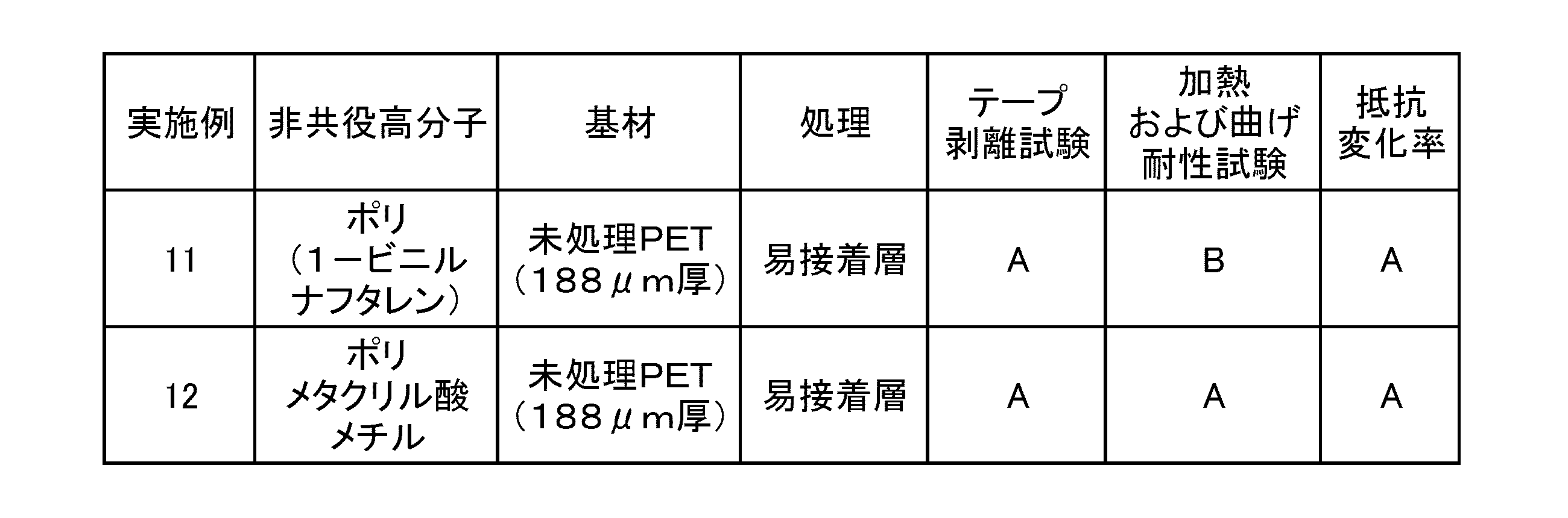
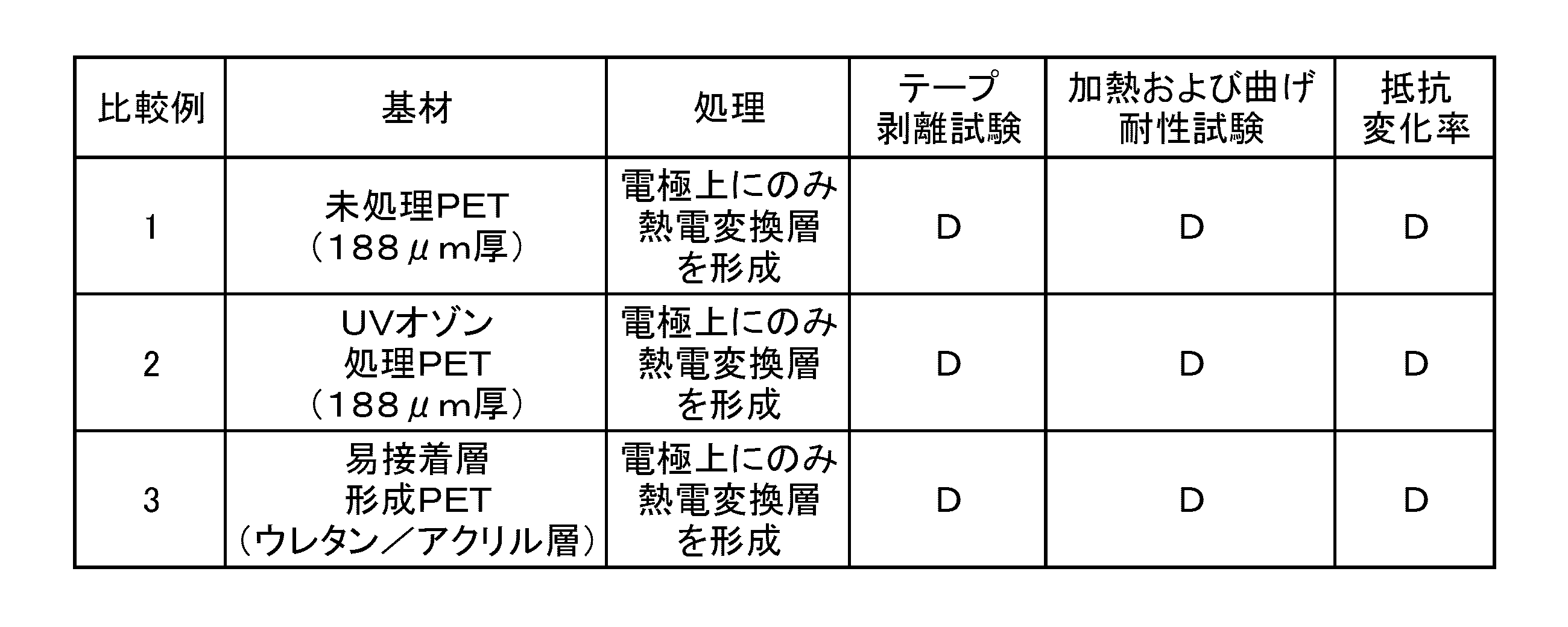
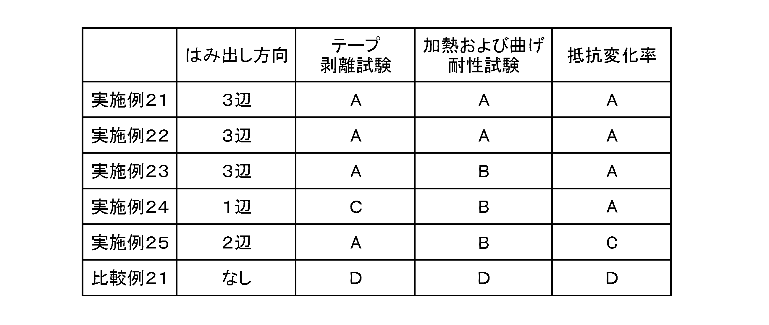
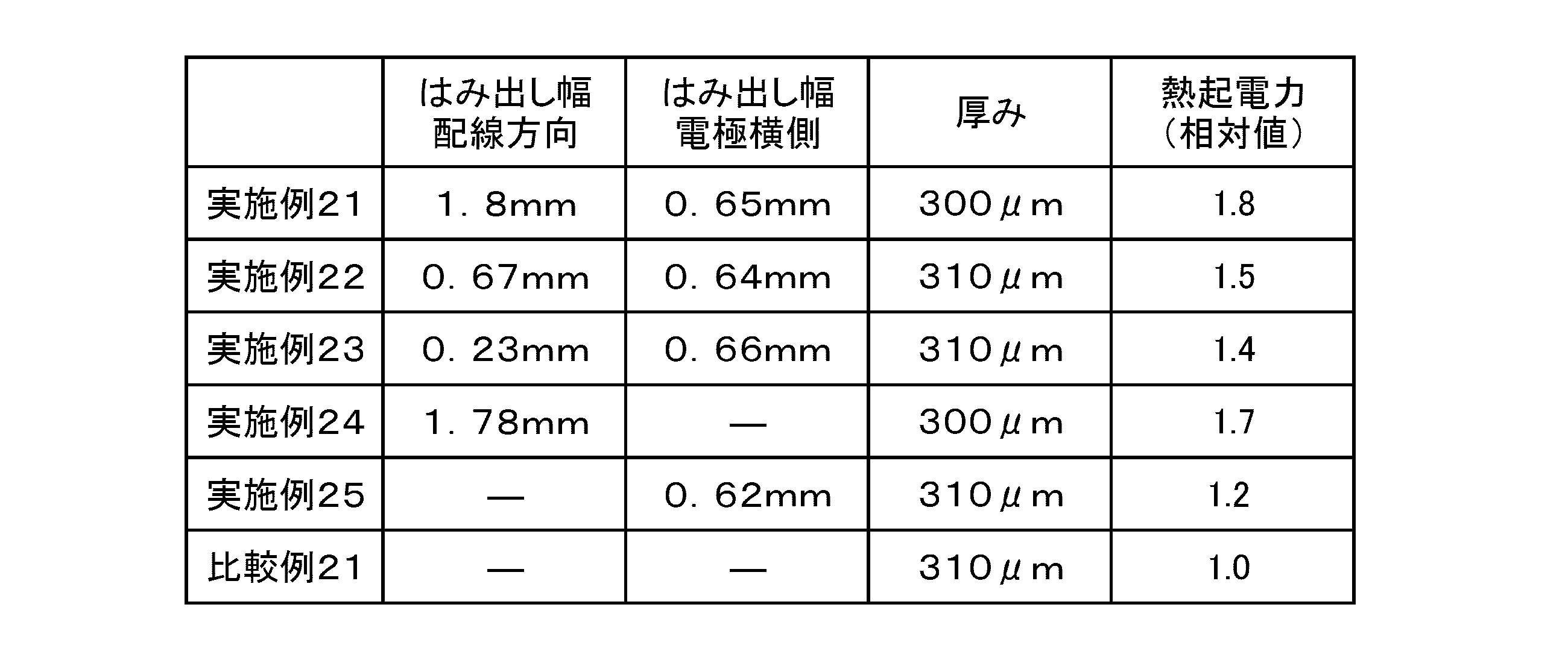
実施例1から10の評価結果から、本発明により熱電変換層は基材との接着性が向上し、テープ剥離試験および、加熱および曲げ耐性試験において、良好な性能を示すことが明らかになった。特に、PETおよびPENフィルムの基材に易接着層を形成したものは、易接着層により濡れ性が向上した状態を維持できたことによって、熱電変換層の接着性が良好になったものといえる。また、ポリイミド基板にUVオゾン処理をしたものについては、表面処理に伴い、イミド環が開環し、濡れ性が向上した状態を維持し、かつ基材の熱膨張率が低いため、より優れた加熱および曲げ耐性を示したといえる。
また、熱電変換層を電極(金電極)の3辺外側の基材に接着するように、カーボンナノチューブ分散ペーストを印刷、形成することで、抵抗変化率が良好な結果となった。
一方、実施例24の抵抗変化率の評価結果から、接続される配線下方において、電極の1辺のみで熱電変換層をはみだし、基材に接着すると、リークがなく優れたものとなった。さらに、実施例25の抵抗変化率の評価結果から、配線方向ではない電極の2辺で熱電変換層をはみだし、基材に接着するようにしても、リークは実用上使用できる状態であった。
また、熱電変換層を電極(金電極)の3辺外側の基材に接着するように、カーボンナノチューブ分散ペーストを印刷、形成することで、抵抗変化率が良好な結果となった。
一方、実施例24の抵抗変化率の評価結果から、接続される配線下方において、電極の1辺のみで熱電変換層をはみだし、基材に接着すると、リークがなく優れたものとなった。さらに、実施例25の抵抗変化率の評価結果から、配線方向ではない電極の2辺で熱電変換層をはみだし、基材に接着するようにしても、リークは実用上使用できる状態であった。
さらに実施例11、12の評価結果から非共役高分子として、ビニルポリマーや(メタ)アクリルポリマーを用いても、本発明の構成を採用することにより熱電変換層と基材との密着性が向上し、テープ剥離試験および、加熱および曲げ耐性試験において、良好な性能を示すことが明らかになった。なお、(メタ)アクリルポリマー、ポリカーボネートは、ビニルポリマーに比べ、加熱および曲げ耐性試験において、より良好な性能を示すことが明らかになった。
実施例21~25は、比較例21に比べ、本発明により、基材との接着性が向上し、テープ剥離試験および、加熱および曲げ耐性試験において、良好な性能を示すことが明らかになった。また、熱電変換層3の基材1上へのはみ出し方向が多い、すなわち接着面積が大きいほど、テープ剥離試験および、加熱および曲げ耐性試験において、特に良好な結果を示した。
さらに、熱電発電モジュール評価結果からは、実施例21~24において、良好な熱起電力が得られ、銀ペーストの配線が配線方向にはみ出すことで、高い熱起電力を得られ、また、はみ出し幅を大きくすることで、より高い熱起電力を得られることができた。
さらに、テープ剥離試験および、加熱および曲げ耐性試験の良好な熱電変換素子と、高い熱起電力を示す熱電発電モジュールを両立するには、実施例21、22および23から、熱電変換層3の膜厚よりはみ出し幅を大きくすることが有効であることが明らかになった。
さらに、熱電発電モジュール評価結果からは、実施例21~24において、良好な熱起電力が得られ、銀ペーストの配線が配線方向にはみ出すことで、高い熱起電力を得られ、また、はみ出し幅を大きくすることで、より高い熱起電力を得られることができた。
さらに、テープ剥離試験および、加熱および曲げ耐性試験の良好な熱電変換素子と、高い熱起電力を示す熱電発電モジュールを両立するには、実施例21、22および23から、熱電変換層3の膜厚よりはみ出し幅を大きくすることが有効であることが明らかになった。
比較例1、2および3において、電極(金電極)上にのみ形成した熱電変換素子は、テープ剥離試験や加熱および曲げ耐性試験により、電極-熱電変換層間での剥離が発生した。電極と熱電変換層のバインダーとの相互作用が小さいため、接着性が低いことが原因と推定される。また、フィルムなど有機物への表面処理と異なり、電極上には水酸基やカルボン酸基の導入がなく、電極へ表面処理は洗浄以外の効果がないために、密着性が向上しないと予想される。さらに、電極端面の被覆が不十分で、電極-配線(金電極-銀ペースト)間のリークにより、抵抗変化が発生した。
本発明をその実施例とともに説明したが、我々は特に指定しない限り我々の発明を説明のどの細部においても限定しようとするものではなく、添付の請求の範囲に示した発明の精神と範囲に反することなく幅広く解釈されるべきであると考える。
本願は、2013年3月29日に日本国で特許出願された特願2013-073480に基づく優先権を主張するものであり、これはここに参照してその内容を本明細書の記載の一部として取り込む。
1 基材
2 電極
2a 配線が接続される部分
3 熱電変換層
3a 熱電変換層が形成される領域
4 配線
5 熱電変換素子
6 易接着層
7 表面改質層
8 導電性樹脂層
9 バンク
10 熱電発電モジュール
11 フレキシブル基材
20 熱電発電装置
30 2次電池
31 DC-DCコンバーター
32 2次電池制御IC
34 ケーブル
40 電子機器
50 発熱源
2 電極
2a 配線が接続される部分
3 熱電変換層
3a 熱電変換層が形成される領域
4 配線
5 熱電変換素子
6 易接着層
7 表面改質層
8 導電性樹脂層
9 バンク
10 熱電発電モジュール
11 フレキシブル基材
20 熱電発電装置
30 2次電池
31 DC-DCコンバーター
32 2次電池制御IC
34 ケーブル
40 電子機器
50 発熱源
Claims (10)
- 樹脂製の基材と、
前記基材上に配した複数の電極と、
前記電極の配線が接続される部分を残して前記各電極を個々に被覆する樹脂製の熱電変換層とを有し、
前記熱電変換層が、前記電極の配線が接続される部分を除く前記電極の周囲の前記基材と接着している
熱電発電モジュール。 - 少なくとも前記熱電変換層に接続される配線下方において、前記熱電変換層が前記電極の周囲の前記基材と接着している
請求項1記載の熱電発電モジュール。 - 少なくとも前記熱電変換層に接続される配線下方において、前記熱電変換層が前記電極の周囲の前記基材と接着しており、
前記熱電変換層と前記基材との接着部の幅が前記熱電変換層の厚みより広いことを特徴とする
請求項1または2に記載の熱電発電モジュール。 - 少なくとも前記基材と前記熱電変換層との間に易接着層を有し、
前記熱電変換層が、前記易接着層を接着層として、前記電極の配線が接続される部分を除く前記電極の周囲の前記基材と接着している
請求項1から3のいずれか1項に記載の熱電発電モジュール。 - 少なくとも前記基材および前記電極と、前記熱電変換層との間に導電性樹脂層を有し、
前記熱電変換層が、前記導電性樹脂層を接着層として、配線が接続される部分を除く前記電極およびその周囲の前記基材と接着している
請求項1から3のいずれか1項に記載の熱電発電モジュール。 - 前記導電性樹脂層と比べて前記熱電変換層の導電率が高い請求項5記載の熱電発電モジュール
- 少なくとも前記熱電変換層が接着される前記熱電変換層の下地表面はエネルギー線が照射された表面改質面を有し、
前記熱電変換層が、前記表面改質面を接着面として、前記電極の配線が接続される部分を除く前記電極の周囲の前記基材と接着している
請求項1から6のいずれか1項に記載の熱電発電モジュール。 - 前記熱電変換層とこの熱電変換層に被覆された電極に隣接する別の電極の前記配線が接続される部分とを電気的に接続する配線を有する請求項1から7のいずれか1項に記載の熱電発電モジュール。
- 前記熱電変換層の出力部に電気的に接続される2次電池を実装した
請求項1から8のいずれか1項に記載の熱電発電モジュール。 - 前記2次電池に接続した電子機器を実装した
請求項9に記載の熱電発電モジュール。
Priority Applications (1)
| Application Number | Priority Date | Filing Date | Title |
|---|---|---|---|
| US14/857,228 US9786830B2 (en) | 2013-03-29 | 2015-09-17 | Thermoelectric generation module |
Applications Claiming Priority (2)
| Application Number | Priority Date | Filing Date | Title |
|---|---|---|---|
| JP2013073480A JP5931790B2 (ja) | 2013-03-29 | 2013-03-29 | 熱電発電モジュール |
| JP2013-073480 | 2013-03-29 |
Related Child Applications (1)
| Application Number | Title | Priority Date | Filing Date |
|---|---|---|---|
| US14/857,228 Continuation US9786830B2 (en) | 2013-03-29 | 2015-09-17 | Thermoelectric generation module |
Publications (1)
| Publication Number | Publication Date |
|---|---|
| WO2014156871A1 true WO2014156871A1 (ja) | 2014-10-02 |
Family
ID=51623850
Family Applications (1)
| Application Number | Title | Priority Date | Filing Date |
|---|---|---|---|
| PCT/JP2014/057507 Ceased WO2014156871A1 (ja) | 2013-03-29 | 2014-03-19 | 熱電発電モジュール |
Country Status (3)
| Country | Link |
|---|---|
| US (1) | US9786830B2 (ja) |
| JP (1) | JP5931790B2 (ja) |
| WO (1) | WO2014156871A1 (ja) |
Cited By (1)
| Publication number | Priority date | Publication date | Assignee | Title |
|---|---|---|---|---|
| US20220190748A1 (en) * | 2019-04-17 | 2022-06-16 | Gce Institute Inc. | Power generation element, power generation device, electronic apparatus, and method for manufacturing power generation element |
Families Citing this family (15)
| Publication number | Priority date | Publication date | Assignee | Title |
|---|---|---|---|---|
| JP6276726B2 (ja) * | 2015-03-18 | 2018-02-07 | 富士フイルム株式会社 | 熱電変換素子 |
| US10459430B2 (en) * | 2015-09-11 | 2019-10-29 | Xerox Corporation | Method and system for variable data printing in a 3D print system |
| JP6739072B2 (ja) * | 2015-10-15 | 2020-08-12 | 国立研究開発法人産業技術総合研究所 | 熱電変換モジュールの作製方法 |
| KR101793462B1 (ko) * | 2015-12-23 | 2017-11-06 | 울산과학기술원 | 스핀 열전 소자 구조체 |
| CH712996A1 (de) * | 2016-09-30 | 2018-04-13 | Hoffmann Neopac Ag | Tube und Tubenkörper mit einer elektronischen Vorrichtung. |
| KR102095243B1 (ko) * | 2018-04-04 | 2020-04-01 | 엘지이노텍 주식회사 | 열전소자 |
| WO2019194539A1 (ko) * | 2018-04-04 | 2019-10-10 | 엘지이노텍 주식회사 | 열전소자 |
| EP3579288B1 (en) * | 2018-06-04 | 2021-04-21 | Polar Electro Oy | Thermoelectric energy generator arrangement |
| JP7587509B2 (ja) | 2019-01-23 | 2024-11-20 | エルジー イノテック カンパニー リミテッド | 熱電素子 |
| CN113853738A (zh) * | 2019-05-21 | 2021-12-28 | Gce研究开发有限公司 | 发电元件、发电装置、电子设备以及发电元件的制造方法 |
| JP7627940B2 (ja) * | 2021-03-18 | 2025-02-07 | 国立研究開発法人産業技術総合研究所 | 熱電変換層を有する積層体とその製造方法、及び発電モジュール |
| JP7749934B2 (ja) * | 2021-05-12 | 2025-10-07 | 日本電気株式会社 | ボロメータおよびその製造方法 |
| US12405038B2 (en) | 2022-02-25 | 2025-09-02 | Tark Thermal Solutions, Inc. | Thermoelectric assemblies with plastic moisture barriers |
| EP4482281A4 (en) * | 2022-03-08 | 2025-05-21 | Denka Company Limited | THERMOELECTRIC CONVERSION MODULE AND MANUFACTURING METHOD THEREFOR |
| WO2026019270A1 (ko) * | 2024-07-18 | 2026-01-22 | 주식회사 나인테크 | 열전소자 및 열전모듈 |
Citations (6)
| Publication number | Priority date | Publication date | Assignee | Title |
|---|---|---|---|---|
| JPH0846249A (ja) * | 1994-07-27 | 1996-02-16 | Seiko Instr Inc | 熱電素子モジュール及び熱電素子モジュールを用いた携帯電子機器 |
| JP2005209718A (ja) * | 2004-01-20 | 2005-08-04 | Ritsumeikan | 熱電変換デバイス |
| WO2008029451A1 (en) * | 2006-09-05 | 2008-03-13 | Pioneer Corporation | Thermal sound generating device |
| JP2008182092A (ja) * | 2007-01-25 | 2008-08-07 | Toyobo Co Ltd | 熱電変換モジュール |
| JP2011029295A (ja) * | 2009-07-23 | 2011-02-10 | Fujitsu Ltd | 熱電変換モジュール及びその製造方法 |
| JP2011192923A (ja) * | 2010-03-16 | 2011-09-29 | Fujitsu Ltd | 熱電変換装置及びその製造方法 |
Family Cites Families (8)
| Publication number | Priority date | Publication date | Assignee | Title |
|---|---|---|---|---|
| JPS63102382A (ja) * | 1986-10-20 | 1988-05-07 | Mitsubishi Heavy Ind Ltd | 薄膜型熱電変換素子モジユ−ルの製造方法とその構造体 |
| US6936653B2 (en) * | 2002-03-14 | 2005-08-30 | Carbon Nanotechnologies, Inc. | Composite materials comprising polar polymers and single-wall carbon nanotubes |
| JP2005340565A (ja) | 2004-04-27 | 2005-12-08 | Kyocera Corp | 熱電交換モジュール用セラミック基板 |
| JP2007035907A (ja) | 2005-07-27 | 2007-02-08 | Kyocera Corp | 熱電モジュール |
| JP4404127B2 (ja) * | 2007-09-28 | 2010-01-27 | ヤマハ株式会社 | 熱電モジュール用基板およびこの基板を用いた熱電モジュール |
| US20100095995A1 (en) * | 2008-10-17 | 2010-04-22 | Ishikawa Prefectural Government | Thermoelectric conversion elements, thermoelectric conversion modules and a production method of the thermoelectric conversion modules |
| JP2010199276A (ja) | 2009-02-25 | 2010-09-09 | Konica Minolta Holdings Inc | 熱電変換素子およびその製造方法 |
| US8460747B2 (en) * | 2010-03-04 | 2013-06-11 | Guardian Industries Corp. | Large-area transparent conductive coatings including alloyed carbon nanotubes and nanowire composites, and methods of making the same |
-
2013
- 2013-03-29 JP JP2013073480A patent/JP5931790B2/ja active Active
-
2014
- 2014-03-19 WO PCT/JP2014/057507 patent/WO2014156871A1/ja not_active Ceased
-
2015
- 2015-09-17 US US14/857,228 patent/US9786830B2/en active Active
Patent Citations (6)
| Publication number | Priority date | Publication date | Assignee | Title |
|---|---|---|---|---|
| JPH0846249A (ja) * | 1994-07-27 | 1996-02-16 | Seiko Instr Inc | 熱電素子モジュール及び熱電素子モジュールを用いた携帯電子機器 |
| JP2005209718A (ja) * | 2004-01-20 | 2005-08-04 | Ritsumeikan | 熱電変換デバイス |
| WO2008029451A1 (en) * | 2006-09-05 | 2008-03-13 | Pioneer Corporation | Thermal sound generating device |
| JP2008182092A (ja) * | 2007-01-25 | 2008-08-07 | Toyobo Co Ltd | 熱電変換モジュール |
| JP2011029295A (ja) * | 2009-07-23 | 2011-02-10 | Fujitsu Ltd | 熱電変換モジュール及びその製造方法 |
| JP2011192923A (ja) * | 2010-03-16 | 2011-09-29 | Fujitsu Ltd | 熱電変換装置及びその製造方法 |
Cited By (1)
| Publication number | Priority date | Publication date | Assignee | Title |
|---|---|---|---|---|
| US20220190748A1 (en) * | 2019-04-17 | 2022-06-16 | Gce Institute Inc. | Power generation element, power generation device, electronic apparatus, and method for manufacturing power generation element |
Also Published As
| Publication number | Publication date |
|---|---|
| US20160005948A1 (en) | 2016-01-07 |
| JP2014197647A (ja) | 2014-10-16 |
| JP5931790B2 (ja) | 2016-06-08 |
| US9786830B2 (en) | 2017-10-10 |
Similar Documents
| Publication | Publication Date | Title |
|---|---|---|
| JP5931790B2 (ja) | 熱電発電モジュール | |
| McCoul et al. | Recent advances in stretchable and transparent electronic materials | |
| US20160104829A1 (en) | Thermoelectric conversion element and thermoelectric conversion module | |
| CN103403900B (zh) | 热电转换材料和使用该材料的挠性热电转换元件 | |
| US10403859B2 (en) | Organic light-emitting device with graphene electrode layer and method of manufacturing the same | |
| JP6162666B2 (ja) | 熱電変換装置 | |
| WO2009152146A1 (en) | Improved cnt/topcoat processes for making a transplant conductor | |
| JP5748350B2 (ja) | 透明導電フィルム、その製造方法、フレキシブル有機電子デバイス、及び、有機薄膜太陽電池 | |
| JP5565038B2 (ja) | 電界効果型トランジスタ及びその製造方法並びに画像表示装置 | |
| JP2015050426A (ja) | 熱電変換素子 | |
| JP2015092557A (ja) | 熱電変換モジュール | |
| JP5184856B2 (ja) | P―n接合素子及びその製造方法、p−n接合素子を利用するダイオード | |
| KR102746997B1 (ko) | 면상 발열체의 제조방법 | |
| CN108349216A (zh) | 透明导电层叠层用膜、其制造方法、以及透明导电膜 | |
| JP2009252437A (ja) | 透明導電性フィルム | |
| CN105207517A (zh) | 摩擦发电装置及其制造方法 | |
| JPWO2021048923A1 (ja) | 電極の製造方法および光電変換素子の製造方法 | |
| KR20220102980A (ko) | 방열 및 전자파 차폐 복합재료, 이를 구비하는 전자 소자 패키지 및 이의 제조방법 | |
| Kang et al. | Adaptive Fabrication of a Flexible Electrode by Optically Self‐Selected Interfacial Adhesion and Its Application to Highly Transparent and Conductive Film | |
| JP2019102499A (ja) | 積層体の製造方法、および積層体 | |
| KR20150039249A (ko) | 표시장치 | |
| JP2009088164A (ja) | 放熱スラリー及びそれを用いた電子部品 | |
| US11510323B2 (en) | Conductive laminated structure, a manufacturing method thereof, and a display panel | |
| WO2016136363A1 (ja) | 熱電変換素子および熱電変換モジュール | |
| KR101495239B1 (ko) | 변이층을 이용한 도전 배선이 함입된 유연 기판 제조 방법 및 이에 의해 제조된 도전 배선이 함입된 유연 기판 |
Legal Events
| Date | Code | Title | Description |
|---|---|---|---|
| 121 | Ep: the epo has been informed by wipo that ep was designated in this application |
Ref document number: 14773461 Country of ref document: EP Kind code of ref document: A1 |
|
| NENP | Non-entry into the national phase |
Ref country code: DE |
|
| 122 | Ep: pct application non-entry in european phase |
Ref document number: 14773461 Country of ref document: EP Kind code of ref document: A1 |