US9786830B2 - Thermoelectric generation module - Google Patents
Thermoelectric generation module Download PDFInfo
- Publication number
- US9786830B2 US9786830B2 US14/857,228 US201514857228A US9786830B2 US 9786830 B2 US9786830 B2 US 9786830B2 US 201514857228 A US201514857228 A US 201514857228A US 9786830 B2 US9786830 B2 US 9786830B2
- Authority
- US
- United States
- Prior art keywords
- thermoelectric conversion
- electrode
- layer
- conversion layer
- thermoelectric
- Prior art date
- Legal status (The legal status is an assumption and is not a legal conclusion. Google has not performed a legal analysis and makes no representation as to the accuracy of the status listed.)
- Active
Links
Images






Classifications
-
- H—ELECTRICITY
- H10—SEMICONDUCTOR DEVICES; ELECTRIC SOLID-STATE DEVICES NOT OTHERWISE PROVIDED FOR
- H10N—ELECTRIC SOLID-STATE DEVICES NOT OTHERWISE PROVIDED FOR
- H10N10/00—Thermoelectric devices comprising a junction of dissimilar materials, i.e. devices exhibiting Seebeck or Peltier effects
- H10N10/10—Thermoelectric devices comprising a junction of dissimilar materials, i.e. devices exhibiting Seebeck or Peltier effects operating with only the Peltier or Seebeck effects
- H10N10/17—Thermoelectric devices comprising a junction of dissimilar materials, i.e. devices exhibiting Seebeck or Peltier effects operating with only the Peltier or Seebeck effects characterised by the structure or configuration of the cell or thermocouple forming the device
-
- H01L35/32—
-
- H01L35/08—
-
- H01L35/10—
-
- H01L35/24—
-
- H01L37/00—
-
- H—ELECTRICITY
- H01—ELECTRIC ELEMENTS
- H01M—PROCESSES OR MEANS, e.g. BATTERIES, FOR THE DIRECT CONVERSION OF CHEMICAL ENERGY INTO ELECTRICAL ENERGY
- H01M10/00—Secondary cells; Manufacture thereof
- H01M10/42—Methods or arrangements for servicing or maintenance of secondary cells or secondary half-cells
- H01M10/425—Structural combination with electronic components, e.g. electronic circuits integrated to the outside of the casing
-
- H—ELECTRICITY
- H10—SEMICONDUCTOR DEVICES; ELECTRIC SOLID-STATE DEVICES NOT OTHERWISE PROVIDED FOR
- H10N—ELECTRIC SOLID-STATE DEVICES NOT OTHERWISE PROVIDED FOR
- H10N10/00—Thermoelectric devices comprising a junction of dissimilar materials, i.e. devices exhibiting Seebeck or Peltier effects
- H10N10/80—Constructional details
- H10N10/81—Structural details of the junction
- H10N10/817—Structural details of the junction the junction being non-separable, e.g. being cemented, sintered or soldered
-
- H—ELECTRICITY
- H10—SEMICONDUCTOR DEVICES; ELECTRIC SOLID-STATE DEVICES NOT OTHERWISE PROVIDED FOR
- H10N—ELECTRIC SOLID-STATE DEVICES NOT OTHERWISE PROVIDED FOR
- H10N10/00—Thermoelectric devices comprising a junction of dissimilar materials, i.e. devices exhibiting Seebeck or Peltier effects
- H10N10/80—Constructional details
- H10N10/82—Interconnections
-
- H—ELECTRICITY
- H10—SEMICONDUCTOR DEVICES; ELECTRIC SOLID-STATE DEVICES NOT OTHERWISE PROVIDED FOR
- H10N—ELECTRIC SOLID-STATE DEVICES NOT OTHERWISE PROVIDED FOR
- H10N10/00—Thermoelectric devices comprising a junction of dissimilar materials, i.e. devices exhibiting Seebeck or Peltier effects
- H10N10/80—Constructional details
- H10N10/85—Thermoelectric active materials
- H10N10/856—Thermoelectric active materials comprising organic compositions
-
- H—ELECTRICITY
- H10—SEMICONDUCTOR DEVICES; ELECTRIC SOLID-STATE DEVICES NOT OTHERWISE PROVIDED FOR
- H10N—ELECTRIC SOLID-STATE DEVICES NOT OTHERWISE PROVIDED FOR
- H10N15/00—Thermoelectric devices without a junction of dissimilar materials; Thermomagnetic devices, e.g. using the Nernst-Ettingshausen effect
-
- Y—GENERAL TAGGING OF NEW TECHNOLOGICAL DEVELOPMENTS; GENERAL TAGGING OF CROSS-SECTIONAL TECHNOLOGIES SPANNING OVER SEVERAL SECTIONS OF THE IPC; TECHNICAL SUBJECTS COVERED BY FORMER USPC CROSS-REFERENCE ART COLLECTIONS [XRACs] AND DIGESTS
- Y02—TECHNOLOGIES OR APPLICATIONS FOR MITIGATION OR ADAPTATION AGAINST CLIMATE CHANGE
- Y02E—REDUCTION OF GREENHOUSE GAS [GHG] EMISSIONS, RELATED TO ENERGY GENERATION, TRANSMISSION OR DISTRIBUTION
- Y02E60/00—Enabling technologies; Technologies with a potential or indirect contribution to GHG emissions mitigation
- Y02E60/10—Energy storage using batteries
Definitions
- the present invention relates to a thermoelectric generation module.
- thermoelectric conversion material that allows mutual conversion between heat energy and electric energy is used for a thermoelectric conversion element, such as a thermoelectric generation device and a Peltier device.
- thermoelectric generation module applying the thermoelectric conversion material, such an advantage is obtained that heat energy can be directly converted into electric power, and that a movable part is not required, and thus the thermoelectric generation module is used for a power supply for a wrist watch operated by body temperature, a medical equipment, a power supply for remote districts which utilizes a wasted heat, a space power supply, or the like.
- thermoelectric generation module is often used by looping it around the curved surface, such as a pipe, an arm, a trunk of the body, and the like. It is therefore required that even if the thermoelectric generation module is inflected, a thermoelectric conversion layer follows the inflection, without being peeled-off from a base material of the thermoelectric generation module.
- Patent Literatures 1 and 2 disclose that a thermoelectric element is disposed on an electrode.
- Patent Literature 3 discloses that, in accordance with a printing method, after forming a resin-made insulator having voids of 100 rows and 3 columns on a polyethylene terephthalate film support, a conductive layer is formed in each of the voids, and further a thermoelectric conversion layer (p-type semiconductor element and n-type semiconductor element) is formed.
- thermoelectric element (the thermoelectric conversion layer) is formed only on an electrode (a conductive layer).
- thermoelectric element is formed only on an electrode
- thermoelectric conversion layer is formed only on a conductive layer.
- the present invention is to provide a thermoelectric generation module having improved adhesion between a thermoelectric conversion layer or/and an electrode and a base material (i.e. a substrate), thereby improving flexibility.
- thermoelectric generation module of the present invention by the reason that the thermoelectric conversion layer is adhered to the base material around the electrode, a stronger adhesion force is obtained than the adhesion on the electrode and, therefore, the thermoelectric conversion layer becomes difficult to peel-off from the base material. As a result, flexibility of the thermoelectric generation module is improved, so that the thermoelectric generation module having resistance to bending can be provided.
- thermoelectric generation module This allows mounting to the flexible base material and lowering of peeling-off of the thermoelectric conversion layer due to bending, or associated with thermal expansion or thermal shrinkage, thereby for enabling provision of a reliable thermoelectric generation module.
- FIG. 1( a ) and FIG. 1( b ) each are a view schematically showing a configuration of the thermoelectric conversion element array of the thermoelectric generation module for explaining an embodiment of the present invention
- FIG. 1( a ) is a plan view
- FIG. 1( b ) is an A-A′ line cross-sectional view in FIG. 1( a ) .
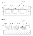
- FIG. 2( a ) and FIG. 2( b ) each are a view showing an example of the thermoelectric conversion element array;
- FIG. 2( a ) is a plan view; and
- FIG. 2( b ) is a cross-sectional view in the array direction.
- FIG. 3 is a plan view showing an example of the thermoelectric generator constituted by arranging thermoelectric conversion elements in a matrix on the base material.
- FIG. 4 is a cross-sectional view showing an example of the thermoelectric conversion element of the thermoelectric generation module having the easy adhesion layer formed on the base material.
- FIG. 5 is a cross-sectional view showing an example of the thermoelectric conversion element of the thermoelectric generation module, in which, after forming the electrode on the base material, a surface of the base material is made to have a surface-modified face.
- FIG. 6 is a cross-sectional view showing an example of the thermoelectric conversion element of the thermoelectric generation module, in which, after making a surface of the base material to have a surface-modified face, the electrode is formed on the base material.
- FIG. 7 is a cross-sectional view showing an example of the thermoelectric conversion element of the thermoelectric generation module having formed therein the conductive resin layer coating both the base material and the electrode.
- FIG. 8 is a block view showing a preferable example of the configuration for charging the thermoelectric generation module described in the embodiment.
- FIG. 9 is a block view showing a preferable example of the configuration for discharging the thermoelectric generation module described in the embodiment.
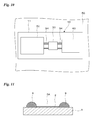
- FIG. 10 is a plan view schematically showing a preferable example of the electronic device mounted on the thermoelectric generation module mounting a thin-film solid secondary battery.
- FIG. 11 is a cross-sectional view showing the base material to be used for ink jetting.
- FIG. 12( a ) and FIG. 12( b ) each are a cross-sectional view showing a resistance measuring method;
- FIG. 12( a ) is a cross-sectional view showing a measuring method of resistance value between the electrode and the thermoelectric conversion element;
- FIG. 12( b ) is a cross-sectional view showing a measuring method of resistance value among the electrode, the thermoelectric conversion element, and the wiring.
- FIG. 13 is a plan view showing a position relationship between the electrode and the thermoelectric conversion layer in Examples 21 to 23.
- FIG. 14 is a plan view showing a position relationship between the electrode and the thermoelectric conversion layer in Example 24.
- FIG. 15 is a plan view showing a position relationship between the electrode and the thermoelectric conversion layer in Example 25.
- thermoelectric generation module of the present invention A detailed explanation about a preferable embodiment of the thermoelectric generation module of the present invention is given below on the basis of FIGS. 1 and 2 . Note that the present invention is not construed as being limited by the explanation of this embodiment.
- thermoelectric generation module 10 of this embodiment has a plurality of electrodes 2 disposed on a principal surface of a resin-made base material 1 , and a resin-made thermoelectric conversion layer 3 that coats each of the electrodes 2 individually while leaving a portion 2 a of the electrode 2 to which a wiring is to be connected.
- the thermoelectric conversion layer 3 is adhered to both a surface of the electrode 2 and the base material 1 around the electrode 2 excluding the portion 2 a of the electrode 2 to which the wiring is to be connected.
- wiring 4 is disposed so as to electrically connect the thermoelectric conversion layer 3 with a portion (not shown) of the other electrode to which a wiring is to be connected, in which the other electrode is adjacent to the electrode 2 ( 21 ) coating the thermoelectric conversion layer 3 .
- the wiring 4 is disposed not to connect to the electrode 2 ( 21 ).
- the graphically-illustrated wiring 4 has a smaller width than the electrode 2 or the thermoelectric conversion layer 3 .
- the width of the wiring 4 may be equal to or broader than the electrode 2 or the thermoelectric conversion layer 3 . In this way, the thermoelectric conversion element 5 of the thermoelectric generation module 10 is constituted.
- thermoelectric conversion element 5 of the thermoelectric generation module 10 is used in such a way that the side of the wiring 4 on the thermoelectric conversion layer 3 acts as a high-temperature side, while the side of the electrode 2 acts as a low-temperature side, and generates an electric energy according to a temperature difference between the wiring 4 and the electrode 2 .
- thermoelectric conversion layer 3 a potential difference is caused by transfer of positive charge (positive hole) from the side of the wiring 4 having a high temperature to the side of the electrode 2 having a low temperature, inside the thermoelectric conversion layer 3 , whereby a thermal electromotive force is generated.
- This electromotive phenomenon is called as Seebeck effect.
- thermoelectric conversion layer 3 there is no particular limitation to the shape or the area, as long as the place is other than the location excluding the portion 2 a of the electrode 2 to which a wiring is to be connected.
- the region of the base material 1 having contact with any 1 side, arbitrary 2 sides, or 3 sides may be used as a region (hereinafter referred to as an “adhesion portion”) to which the thermoelectric conversion layer 3 is adhered.
- the region of the base material 1 having contact with arbitrary 2 sides or 3 sides is preferably used as a adhesion portion 3 a , and all of the regions of the base material 1 having contact with the 3 sides are more preferably used.
- the thermoelectric conversion layer 3 is adhered to the base material 1 around the electrode 2 .
- the region of the base material 1 which has contact with the side of the electrode 2 on the side to which the wiring 4 is connected may be also used as an adhesion portion, as long as short circuit does not occur between the electrode 2 which the thermoelectric conversion layer 3 coats and the wiring 4 which is to be connected to the electrode 2 .
- an adhesion portion By applying such an adhesion portion in this way, the adhesion between the thermoelectric conversion layer 3 and the base material 1 is more consolidated.
- width w of the adhesion portion 3 a there is no particular limitation to the width w of the adhesion portion 3 a , as long as short circuit does not occur among the thermoelectric conversion layer, the electrode, and the wiring, all of which are adjacent to each other.
- the shape of the electrode 2 is a triangle, a polygon, a circle, a tetragon having rounded corners, or the like
- a region of the base material 1 which has contact with a side or a part of the side other than the location excluding the portion 2 a of the electrode 2 to which a wiring is to be connected can be used as an adhesion portion 3 a of the thermoelectric conversion layer 3 .
- the tetragon having rounded corners means a tetragon whose corners have a curvature.
- thermoelectric conversion layer 3 is adhered to the base material 1 in the region below the wiring 4 which is connected to the thermoelectric conversion layer 3 , any short circuit between the wiring 4 and the electrode 2 on the base material 1 can be prevented, and also recombination of electrons generated by a Seebeck effect inside the wiring 4 and positive holes generated by a Seebeck effect inside the thermoelectric conversion layer 3 can be prevented, so that an effect on increase of output power can be expected.
- the thermoelectric conversion layer 3 is adhered to the base material 1 around the electrode 2 . It is preferable that the width w of the adhesion portion 3 a is equal to or wider than the thickness t of the thermoelectric conversion layer 3 . From the viewpoint of a balance between increase of output voltage and adhesiveness, it is more preferable that the width w is at least 2 times wider than the thickness t.
- thermoelectric conversion elements 5 are electrically connected in series with wiring 4 , to constitute the thermoelectric generator 20 of the thermoelectric generation module 10 .
- thermoelectric conversion elements 5 may be arranged in a matrix on the base material 1 , and electrically and sequentially connected in series with the wiring 4 , to constitute the thermoelectric generator 20 of the thermoelectric generation module 10 .
- this is a configuration in which thermoelectric conversion element 5 are sequentially and electrically connected in series in a broken-line shape.
- the number of allays of the thermoelectric conversion element 5 shown in FIG. 3 is one line. The number of allays of the thermoelectric conversion element 5 is therefore determined appropriately, by an electromotive force per one thermoelectric conversion element 5 and an electromotive force as the thermoelectric generator 20 .
- both ends of the thermoelectric conversion elements 5 connected in series act as output terminals 51 and 52 , respectively, to which output wirings 53 and 54 are connected, respectively.
- the output terminals 51 and 52 use may be made of the electrode 2 , the wiring 4 , or an electrode 23 which connects to the wiring 4 , all of which are in the thermoelectric conversion elements 5 .
- thermoelectric conversion element 5 is electrically connected in series. As a result, electric current flows in one direction and thermal electromotive force generated by each thermoelectric conversion element 5 is added, so that a desired electric energy can be generated by output of the electric current to the outside.
- any of base materials such as plastic films having flexibility, and the like are exemplified.
- the plastic films which are inexpensive and have flexibility, are preferred.
- the base material 1 preferably includes specific examples of: a polyester resin film, such as a poly(ethylene terephthalate) film, a poly(ethylene isophthalate) film, a poly(ethylene naphthalate) film, a poly(butylene terephthalate) film, a poly(1,4-cyclohexylene dimethylene terephthalate) film, and a poly(ethylene-2,6-phthalenedicarboxylate) film;
- the plastic film (a resin film) includes: a polyimide film; a polycarbonate film; a polypropylene film; a polyether sulfone film; a cycro-olefin polymer; a poly(ether ether ketone) (PEEK) film; and a triacetyl cellulose (TAC) film; as well as a glass epoxy film, and a liquid crystalline polyester film.
- a polyester resin film such as a poly(ethylene terephthalate) film, a poly(ethylene is
- poly(ether ether ketone), poly(ethylene terephthalate), poly(ethylene naphthalate), polyimide, glass epoxy, and liquid-crystalline polyester are preferred, and poly(ethylene terephthalate), poly(ethylene naphthalate), polyimide, glass epoxy, and liquid crystalline polyester are particularly preferred.
- inorganic or organic fine particles for example, an inorganic filler, such as titanium oxide, calcium carbonate, silica, barium sulfate, silicone, and the like; and an organic filler, such as acryl, benzoguanamine, TEFLON (registered trademark), epoxy, and the like; and an adhesion-improving agent or antistatic agent, such as polyethylene glycol (PEG), sodium dodecyl benzene sulfonate, and the like.
- an inorganic filler such as titanium oxide, calcium carbonate, silica, barium sulfate, silicone, and the like
- organic filler such as acryl, benzoguanamine, TEFLON (registered trademark), epoxy, and the like
- an adhesion-improving agent or antistatic agent such as polyethylene glycol (PEG), sodium dodecyl benzene sulfonate, and the like.
- a polyester film can be formed, by melt-extruding a polyester resin into a film, and subjecting the film to orientation crystallization by a horizontal and vertical biaxial stretching, and then to crystallization by a heat treatment.
- the thickness of the base material 1 there is no particular limitation to the thickness of the base material 1 to be used in this embodiment.
- a film having the thickness of 5 ⁇ m or more and 1,000 ⁇ m or less is used, and from the viewpoint of flexibility, a film having the thickness of 10 ⁇ m or more and 500 ⁇ m or less is preferably used, and a film having the thickness of 10 ⁇ m or more and 250 ⁇ m or less is still more preferably used.
- any of additives such as an ultraviolet absorber, is preferably contained.
- an ultraviolet absorber use may be preferably made of: an oxazole-based, triazine-based, stilbene-based, or coumalin-based ultraviolet absorber.
- the electrode 2 use may be made of any of known materials, including: a metal electrode, such as copper, silver, gold, platinum, nickel, chromium, or copper alloy; a transparent electrode, such as indium tin oxide (ITO), zinc oxide (ZnO), or the like; and the like. Any of copper, gold, platinum, nickel, or copper alloy is preferably used. Any of gold, platinum, or nickel is more preferably used. Alternatively, a solidified metal paste may be used, which has been formed by microparticulating the above metal, and adding a binder and a solvent to the microparticulated metal.
- a metal electrode such as copper, silver, gold, platinum, nickel, chromium, or copper alloy
- a transparent electrode such as indium tin oxide (ITO), zinc oxide (ZnO), or the like
- ITO indium tin oxide
- ZnO zinc oxide
- Any of copper, gold, platinum, nickel, or copper alloy is preferably used.
- a solidified metal paste may be used, which has
- the thermoelectric conversion layer 3 has a carbon nanotube (hereinafter, which may be referred to as CNT) and a resin layer which acts as a binder.
- the resin layer which acts as a binder includes: a vinyl compound, a (meth)acrylate compound, a carbonate compound, and an ester compound.
- the vinyl compound include: polystyrene, poly(vinylnaphthalene), poly(vinyl acetate), poly(vinylphenol), poly(vinylbutyral), and the like.
- Examples of the (meth)acrylate compound include: poly ⁇ methyl(meth)acrylate ⁇ , poly ⁇ ethyl(meth)acrylate ⁇ , poly ⁇ phenoxy (poly)ethyleneglycol (meth)acrylate ⁇ , poly ⁇ benzyl(meth)acrylate ⁇ , and the like.
- Examples of the carbonate compound include: bisphenol Z-type polycarbonate, bisphenol C-type polycarbonate, and the like.
- Examples of the ester compound include: non-crystalline polyesters.
- Preferable examples thereof include: poly(vinylbutyral), a (meth)acrylate compound, a carbonate compound, and an ester compound. More preferable examples thereof include: poly(vinylbutyral), poly ⁇ phenoxy(poly)ethyleneglycol (meth)acrylate ⁇ , poly ⁇ benzyl(meth)acrylate ⁇ , and a non-crystalline polyester.
- any of nanocarbons may be contained, such as carbon nanohorn, carbon nanocoil, carbon nanobeads, graphite, graphene, amorphous carbon, and the like.
- the wiring 4 can be formed by utilizing any of a conductive paste having dispersed therein conductive fine-particles, such as silver, carbon, and the like, or a conductive paste containing a metal nanowire, such as silver, copper, aluminum, and the like.
- Utilization of the conductive paste enables wiring which follows a difference in level between a top surface of the thermoelectric conversion layer and the electrode on the base material, so that connection can be achieved without disconnection of worn(s) and contact failure. As a result, a reliable module generating high-output power can be formed.
- wiring may be achieved, by utilizing any of known conductive materials including a metal, such as gold, silver, copper, and nickel, an alloy of any of these metals, an oxide semiconductor material, such as indium tin oxide (ITO), and the like, according to a combination with sputtering, vacuum deposition and a metal mask method.
- a metal such as gold, silver, copper, and nickel
- an alloy of any of these metals such as gold, silver, copper, and nickel
- an oxide semiconductor material such as indium tin oxide (ITO), and the like
- thermoelectric generation module 10 having the thermoelectric generator 20 , a resin-made thermoelectric conversion layer 3 adheres to a resin-made base material 1 around the electrode 2 excluding the portion of the electrode 2 to which a wiring is to be connected, thereby for obtaining a stronger adhesion force than the electrode 2 composed of a metal. This allows improvement in flexibility of the thermoelectric generation module 10 , so that the thermoelectric generation module 10 which has resistance to bending can be provided.
- thermoelectric generation module 10 is excellent in flexibility, because it has the resin-made thermoelectric conversion layer 3 provided on the resin-made base material 1 .
- a part of the thermoelectric conversion layer 3 is adhered to the resin-made base material 1 in such a way as to protrude to the side of the resin-made base material 1 over the electrode 2 , thereby for becoming adhesion property between the base material 1 and the thermoelectric conversion layer 3 strong.
- This makes it difficult for the thermoelectric conversion layer 3 to be peeled-off from above the electrode 2 , even if the base material 1 is bent. As a result, durability to bending can be obtained, thereby for attaining resistance to the repeated use.
- thermoelectric conversion layer 3 is made of a resin, and therefore it can be prepared by coating. This enables the thermoelectric conversion layer 3 to be prepared so that adhesion property with respect to the base material 1 is consolidated much more, without damaging the base material 1 .
- the thermoelectric generation module 10 preferably has an easy adhesion layer 6 which enhances surface adhesion property.
- the electrode 2 is disposed on a surface of the easy adhesion layer 6 as an adhesion layer, and the thermoelectric conversion layer 3 is adhered to the easy adhesion layer 6 around the electrode 2 excluding the portion (see FIG. 1 ) of the electrode 2 to which a wiring is connected.
- Materials of the easy adhesion layer 6 include gelatin, a poly(vinyl alcohol) (PVA), an acrylic resin, a polyurethane resin, a polyester resin, or the like.
- PVA poly(vinyl alcohol)
- an acrylic resin, a polyurethane resin, and a polyester resin are exemplified.
- a cross-linking agent such as a carbodiimide cross-linking agent, an isocyanate cross-linking agent, a melamine cross-linking agent, or the like may be contained therein.
- thermoelectric conversion layer 3 By forming the easy adhesion layer 6 , an adhesion force of the thermoelectric conversion layer 3 can be further enhanced.
- a surface-modified layer 7 is been formed, which has a surface-modified face obtained by irradiating energy ray on the surface of the base material 1 .
- a surface-modified layer 7 is been formed, which has a surface-modified face obtained by irradiating energy ray on the surface of the base material 1 .
- the surface-modified layer 7 is preferably formed at least on the surface of the base material 1 to be located in the back surface portion of the thermoelectric conversion layer 3 .
- a surface-modification treatment which is performed by energy-ray irradiation it is possible to use any of known treatments, such as a corona treatment using corona discharge, a plasma treatment with exposure to plasma atmosphere, a UV ozone treatment with ultraviolet irradiation in ozone atmosphere, an EB irradiation treatment with electron beam irradiation, and the like.
- the plasma treatment, the corona treatment, and the UV ozone treatment are exemplified.
- a hydroxyl group, a carboxyl group, a basic group, or the like, each of which has polarity can be formed on the surface of the base material, so that adhesion property to the thermoelectric conversion layer 3 are further improved.
- an adhesion force may be increased, by roughening the surface of the base material 1 due to irradiation of energy ray to obtain the surface-modified face, and resultantly by enlarging a surface area to increase an area of adhesion between the base material 1 and the thermoelectric conversion layer 3 .
- the surface-modified layer 7 may be formed on the surface of the easy adhesion layer 6 (see FIG. 4 ) or the surface of the conductive resin layer described below. This enables increase in an adhesion force between the thermoelectric conversion layer 3 and the surface of the easy adhesion layer 6 or the surface of the conductive resin layer, respectively, to be located in the back surface portion of the thermoelectric conversion layer 3 .
- thermoelectric conversion element Having the surface-modified face allows improvement in adhesion property of a metal wiring layer or a protective layer, although these layers are not shown.
- This enables coating of a water-soluble resin high in oxygen barrier property, such as poly(vinylalcohol) (PVA), poly(vinylpyrrolidone) (PVP), or the like, as a protective layer in particular.
- PVA poly(vinylalcohol)
- PVP poly(vinylpyrrolidone)
- thermoelectric conversion layer 3 is arranged on the conductive resin layer 8 , and the thermoelectric conversion layer 3 adheres to the conductive resin layer 8 on a top of the electrode 2 excluding the portion (see FIG. 1 ) of which a wiring on the top of the electrode 2 is to be connected and the conductive resin layer 8 around the electrode 2 .
- the conductivity of the thermoelectric conversion layer 3 is set to a higher level than the conductive resin layer 8 .
- the electrode 2 is coated with the conductive resin layer 8 , and the thermoelectric conversion layer 3 is arranged on this conductive resin layer 8 , and as a result, a direct adhesion between the thermoelectric conversion layer 3 and the electrode 2 (a metal electrode) which is poor in adhesion property, is avoid, which results in adhesion to the conductive resin layer 8 , and which the adhesion property is therefore improved.
- thermoelectric conversion layer 3 since the conductivity of the thermoelectric conversion layer 3 is higher than the conductive resin layer 8 , a flow of electric current between the electrode 2 and the thermoelectric conversion layer 3 becomes easy by intervention of the conductive resin layer 8 between those. In a similar way, by adjusting the conductivity of a wiring (see FIG. 1 ) to a higher level than the conductive resin layer 8 , a flow of electric current between the wiring and the electrode 2 becomes easy. Therefore, since no electric current does flow in the surface direction of the conductive resin layer 8 , the electric current does not flow directly between the electrode 2 and the other electrode 2 adjacent thereto.
- Examples of the conductive resin layer 8 include PEDOT/PSS, PEDOT/NAFION (registered trademark), PEDOT/PVS, and the like; and preferably PEDOT/PSS.
- PEDOT is abbreviation of poly(3,4-ethylenedioxythiophene)
- PSS is abbreviation of poly(4-styrenesulfonate)
- PVS is abbreviation of poly(vinyl sulfonic acid).
- NAFION is a perfluorocarbon material having a sulfonic acid group.
- thermoelectric generation module 10 mounting a thin-film solid secondary battery which is electrically connected to the output portion of the thermoelectric conversion layer 3 , with reference to FIGS. 8 and 9 .
- the power generated by the thermoelectric generation module 10 is a direct-current power, and because of the low voltage, the power, as it is, is difficult to be used for a power required to drive an electronic devise, and the like.
- the voltage obtained by the thermoelectric generation module 10 is therefore increased by means of DC-DC converter 31 .
- the voltage is increased to 4.0 V.
- the secondary battery control IC 32 is composed of: a charging power supply device which produces a direct-current power; and a charge control circuit which controls charging of the buttery, although these devices are not shown.
- the power discharged from the thin-film solid secondary battery as a secondary battery 30 via the secondary battery control IC 32 is transferred to the DC-DC converter 31 .
- the DC-DC converter 31 the voltage is converted to a voltage to be used for electronic devices (not shown) and then the resultant power is output.
- the working voltage of the electronic devices is set to various voltages.
- the voltage is therefore dropped or increased to a working voltage suitable for the electronic devices by the DC-DC converter 31 .
- the voltage is transformed to 3.3 V, and then the power is output.
- DC-DC converter 31 use may be made, for example, of ETC310 manufactured by En Ocean GmbH; LTC3108 and LTC3109 each manufactured by Linear Technology, or the like.
- the secondary battery control IC 32 use may be made, for example, of: LTC4070 and LTC4071 each manufactured by Linear Technology; MAX17710 manufactured by Maxim Integrated Products, or the like.
- MEC201 and MEC220 each manufactured by Infinite Power Solution, or the like.
- thermoelectric generation module mounting a thin-film solid secondary battery as a secondary battery which is electrically connected to an output portion of the thermoelectric conversion layer, with reference to FIG. 10 .
- thermoelectric generation module 10 a thermoelectric generator 20 , a secondary battery 30 (for example, a thin-film solid secondary batter), and an electronic device 40 are connected with a cable 34 mounting a secondary battery control IC 32 (see FIGS. 8 and 9 ) or the like on a flexible base material 11 .
- the cable 34 use is made of: FPC (flexible print circuit) cable; or FFC (flexible flat cable).
- the thermoelectric generation module 10 is put on the heat generation source 50 .
- the secondary battery 30 may be mounted in the thermoelectric generator 20 , although it is not shown.
- Examples of the electronic device 40 include various kinds of electronic devices, such as: an electrocardiogram monitor device, a pulse monitor, a manometer, a wristwatch, a pedometer, a radio transmitting locational information, a thermometer, a vibration meter, or the like.
- the thermoelectric generation module 10 therefore can be preferably used for the intended purposes, such as a power supply for any of those electronic devices, or the like.
- thermoelectric generation module 10 As to the production method of the thermoelectric generation module 10 , it is just necessary that in a known production method of the thermoelectric generation module, the thermoelectric generation module 10 is formed by adhering the thermoelectric conversion layer 3 to the base material 1 in such a way that the thermoelectric conversion layer 3 is protruded over from the electrode 2 .
- the formation of the electrode 2 can be carried out, for example, by a plating method, a patterning method by etching, a sputtering method or an ion plating method using a liftoff process, a sputtering method or an ion plating method using a metal mask, or the like.
- a metal paste in which the above metal is subjected to microparticulation, and then a binder and a solvent are added thereto.
- use may be made of: a screen printing method, or a printing method by a dispenser method. After printing, may be carried out: application of heating for drying; or a heating treatment for decomposition of the binder or sintering of the metal.
- thermoelectric conversion layer 3 is preferably carried out by a printing method, such as: a metal mask printing method of printing a carbon nanotube-dispersed paste; an ink jet printing method of printing by impacting ink droplets of an inkjet-coating liquid containing a carbon nanotube by ink jetting; a screen printing method, or the like.
- a printing method such as: a metal mask printing method of printing a carbon nanotube-dispersed paste; an ink jet printing method of printing by impacting ink droplets of an inkjet-coating liquid containing a carbon nanotube by ink jetting; a screen printing method, or the like.
- the screen printing method for example, there is a method of printing by preparing a printing plate from an etched metal mask, in addition to a method of printing by preparing a printing plate by subjecting a light-sensitive resin placed on a mesh made of ordinary stainless-steel, nylon, or polyester to a patterning exposure and then a development processing.
- the ink jet printing method is carried out as follows.
- the total solid content concentration in a coating liquid for ink jetting is generally 0.05 mass % or more and 30 mass % or less, preferably 0.1 mass % or more and 20 mass % or less, and more preferably 0.1 mass % or more and 10 mass % or less.
- the viscosity of the above coating liquid is, from the viewpoint of ejection stability, generally 1 mPa ⁇ s or more and 30 mPa ⁇ s or less, preferably 1.5 mPa ⁇ s or more and 20 mPa ⁇ s or less, and more preferably 1.5 mPa ⁇ s or more and 15 mPa ⁇ s or less.
- the above coating liquid is used in such a way that the above ingredients are dissolved and dispersed in a prescribed organic solvent, to prepare a coating liquid, and the coating liquid is filtrated using a filter and then coated on the following prescribed support or layer.
- the filter for use in the filtration is preferably a poly(tetrafluoroethylene)-made, polyethylene-made, or nylon-made filter having a pore size of 2.0 ⁇ m or less, and more preferably 0.5 ⁇ m or less.
- a solvent for dissolving or compatibilizing an organic substance which acts as a thermoelectric material and a solvent for dispersing a conductive nanomaterial
- a known solvent appropriately depending on the organic substance which acts as a thermoelectric material or the conductive nanomaterial.
- the solvent examples include any of known organic solvents, such as an aromatic hydrocarbon solvent, an alcohol solvent, a ketone solvent, an aliphatic hydrocarbon solvent, an amide solvent, a halogenated solvent, and the like.
- aromatic hydrocarbon solvent examples include benzene, toluene, xylene, trimethylbenzene, tetramethylbenzene, cumene, ethylbenzene, methylpropylbenzene, methylisopropylbenzene, tetrahydronaphthalene, and the like.
- xylene, cumene, trimethylbenzene, tetramethylbenzene, and tetrahydronaphthalene are more preferred.
- the alcohol solvent examples include methanol, ethanol, butanol, benzyl alcohol, cyclohexnol, and the like. Of these solvents, benzyl alcohol and cyclohexnol are more preferred.
- ketone solvent examples include 1-octanone, 2-octanone, 1-nonanone, 2-nonanone, acetone, 4-heptanone, 1-hexanone, 2-hexanone, 2-butanone, diisobutyl ketone, cyclohexanone, methylcyclohexanone, phenylacetone, methyl ethyl ketone, methyl isobutyl ketone, acetylacetone, acetonylacetone, ionone, diacetonylalcohol, acetylcarbinol, acetophenone, methyl naphthyl ketone, isophorone, propylene carbonate, and the like. Of these solvents, methyl isobutyl ketone and propylene carbonate are preferred.
- aliphatic hydrocarbon solvent examples include pentane, hexane, octane, decane, and the like. Of these solvents, octane and decane are preferred.
- amide solvent examples include N-metrhyl-2-pyrrolidone, N-etrhyl-2-pyrrolidone, N,N-dimethylacetoamide, N,N-dimethylformamide, 1,3-dimethyl-2-imidazolidinone, and the like. Of these solvents, N-metrhyl-2-pyrrolidone and 1,3-dimethyl-2-imidazolidinone are preferred.
- halogenated solvent examples include chloroform, chlorobenzene, dichlorobenzene, and the like. Of these solvents, chlorobenzene and dichlorobenzene are preferred.
- the above solvents may be used solely, or used in combination of 2 kinds or more thereof.
- the base material 1 for use in the ink jet printing method it is preferred to employ a base material having bank 9 formed in such a way as to surround the outer periphery of the region 3 a in which the thermoelectric conversion layer is formed. That is, the region 3 a in which the thermoelectric conversion layer is formed, is entirely walled by the bank 9 . Therefore, droplets of the coating liquid containing a thermoelectric conversion material which have been ink-jetted by ink jetting can be kept within the bank 9 , whereby a formation of the thermoelectric conversion layer (not shown) having a certain height becomes possible.
- the cross-sectional shape of the bank 9 examples include an arc shape (including a semi-circular shape, and a semi-elliptical shape), a triangular shape, a radial shape, a trapezoidal shape, and the like. It is preferred that the top of the bank 9 does not have a flat part. Therefore, the cross-sectional shape of the bank 9 is preferably a convex-curved shape of the arc shape, semi-elliptical shape, triangular shape, radial shape, and the like.
- the droplets attached to the bank 9 become difficult to be kept on the top of the bank 9 , thereby that they can move effectively to the region 3 a in which the thermoelectric conversion layer is formed, by transferring along a convex-curved side surface of the bank 9 .
- the shape of the bank 9 is more preferably an arc shape or a triangular shape, and more preferably an arc shape.
- Examples of the material of the bank 9 include polyimide, a novolac-based resin, an epoxy resin, an acrylic resin, and the like, and from the viewpoint of liquid-repellent property and heat resistance, a polyimide is preferred.
- the bank may be subjected to a liquid-repellent treatment, if needed.
- a fluorocarbon film may be formed on the bank 9 by chemical vapor deposition (CVD) using tetrafluorocarbon (CF 4 ) as a basic gas.
- CVD chemical vapor deposition
- CF 4 tetrafluorocarbon
- a silane coupling agent having a long chain fluoroalkyl group, or a fluorine polymer may be mixed into the bank.
- Examples of the formation method of the bank 9 include: a method of using a photosensitive resist including a dry resist, polyimide, or a photosensitive glass, and further patterning by UV light and development; a method of coating a resist on an alkali-developable polyimide so as to be a multi-layer, and then using patterning by UV light and development; a method of using patterning by a screen printing using an epoxy resin and a UV cross-linking.
- the region 3 a at which the thermoelectric conversion layer is formed is a region which is surrounded by the bank 9 , and a coating liquid containing an organic substance which acts as a thermoelectric material and a conductive nanomaterial are coated in this region 3 a .
- a layer may be formed by coating a coating liquid containing other organic substances, before or after coating the coating liquid onto the region 3 a which forms the thermoelectric conversion layer
- the heating temperature and time period after coating is not particularly limited, as long as the coating liquid is dried.
- the heating temperature is generally 100° C. or more and 200° C. or less, and preferably 120° C. or more and 160° C. or less.
- the heating time period is generally 1 min or more and 120 min or less, preferably 1 min or more and 60 min or less, and more preferably 1 min or more and 25 min or less.
- thermoelectric conversion layer may be carried out in such a way as to increase the thickness of the thermoelectric conversion layer by repeating a plurality of times of: ink-jet printing and drying by heating. Note that with regards to the drying by heating, it does not mutter whether a solvent component is completely volatilized or not.
- thermoelectric conversion element of Example 1 was prepared below.
- silica fine-particles JA-244 manufactured by Jujo Chemical Co., Ltd. was added, and dispersed by a double roll mill heated at 180° C., thereby for preparing silica-dispersed polystyrene.
- KH SWCNT HP manufactured by KH Chemicals, purity 80%
- a mechanical homogenizer T10 basic ULTRA-TURRAX (trade name) manufactured by IKA Works
- an ultrasonic homogenizer VC-750 (trade name) manufactured by Sonics & Materials Inc.
- a tapered microchip (a probe diameter 6.5 mm)
- a base material made of a poly(ethylene terephthalate) (PET) film was formed, according to the following procedures.
- a PET resin having an intrinsic viscosity of 0.66 obtained by condensation polymerization using germanium (Ge) as a catalyst was dried to a moisture content of 50 ppm or less, and then the heater temperature was set to the range of 280° C. or more and 300° C. or less, and then the resultant dried resin was melted in an extruder.
- the thus-melted PET resin was ejected from a die portion onto a static electricity-applied chilled roll, thereby for obtaining an amorphous base.
- the thus-obtained amorphous base was stretched 3.3 times in the direction of the base travel, and then was stretched 3.8 times in the transverse direction, thereby for obtaining a base material made of 188 ⁇ m-thick PET film.
- Each side of the thus-obtained 188 ⁇ m-thick base material was subjected to a corona discharge treatment, under the conditions of 730 J/m 2 , while transporting the base material at a transportation speed of 105 m/min
- the following first layer coating liquid was coated on each side of the base material by a bar coat method. Further, drying at 180° C. for 1 min, to form the first layers, and then continuously the following second layer coating liquid was coated in a coating amount of 96.25 mg/m 2 on each of the first layers by a bar coat method. After that, by drying at 170° C. for 1 min, a PET film was obtained, which has the first easy adhesion layer and the second easy adhesion layer, coated on each side of the base material.
- a 100 nm-thick chromium film and then a 200 nm-thick gold film were formed so as to be a respective layered film on an A6 size PET film in this order, by ion plating, through the use of a metal mask having portions of 6 ⁇ 9 mm opening formed by etching, thereby for forming an electrode.
- the above-prepared carbon nanotube-dispersed paste 1 was injected through a laser-processed metal mask having 80 portions of 8 ⁇ 9 mm opening and a thickness of 2 mm, followed by planarizing by a squeezee. At this time, in such the configuration as shown in FIG. 1 , the carbon nanotube-dispersed paste 1 was printed on the electrode 2 .
- the PET film was dried by heating on an 80° C. hot plate, thereby for forming a thermoelectric conversion element on the electrode.
- thermoelectric conversion element of Example 2 was prepared below.
- Each side of the 188 ⁇ m-thick PET-film base material prepared in the same manner as in Example 1 was subjected to a corona discharge treatment, under the conditions of 730 J/m 2 , while transporting the base material at a transportation speed of 80 m/min After that, an easy adhesion layer coating liquid having the following formula was coated in a coating amount of 4.4 cm 3 /m 2 on each side of the base material by a bar coat method. Further, drying at 160° C. for 1 min, to form an easy adhesion layer, and thereby that a PET film having the easy adhesion layer coated on each side of the base material was obtained.
- thermoelectric conversion element was prepared in the same manner as in Example 1, except that the PET film formed by coating the easy adhesion layer on each side of the base material was used, in place of the PET film on which the two easy adhesion layers were formed on each side of the base material as in Example 1.
- thermoelectric conversion element of Example 3 was prepared below.
- a 100 nm-thick chromium film and a 200 nm-thick gold film were formed so as to be a respective layered film in this order, by ion plating, through the use of a metal mask having portions of 6 ⁇ 9 mm opening formed by etching, thereby for forming an electrode.
- a surface treatment was carried out, using an atmospheric plasma surface treatment apparatus AP-T02-L120 (manufactured by Sekisui Kagaku), under the conditions of: processing gas nitrogen, gas flow rate 60 L/min, processing speed 2 L/min, applied voltage 155 V, and electric current 1.42 A.
- thermoelectric conversion element was prepared in the same manner as in Example 1.
- thermoelectric conversion element of Example 4 was prepared below.
- thermoelectric conversion element was prepared in the same manner as in Example 3, except that a 125 ⁇ m-thick polyimide film: CAPTON 500V (manufactured by DuPont Toray) was used as a base material, and a UV ozone apparatus: UVO Cleaner 42 (trade name, manufactured by Jelight Company, Inc.) was used in place of the atmospheric plasma surface treatment apparatus, and that a UV-ozone treatment was carried out for 10 min in terms of irradiation time.
- a UV ozone apparatus UVO Cleaner 42 (trade name, manufactured by Jelight Company, Inc.) was used in place of the atmospheric plasma surface treatment apparatus, and that a UV-ozone treatment was carried out for 10 min in terms of irradiation time.
- thermoelectric conversion element of Example 5 was prepared below.
- thermoelectric conversion element was prepared in the same manner as in Example 3, except that the PET film, on which the two easy adhesion layers were formed by coating in the same manner as Example 1, was used as a base material, and that a surface modification treatment was carried out twice, under the conditions of; electrode output 80 W and moving speed of the electrode 1 m/min, using a corona surface-modification apparatus TEC-4AX (manufactured by Kasuga Electric Works), in place of the atmospheric plasma surface treatment apparatus.
- TEC-4AX manufactured by Kasuga Electric Works
- thermoelectric conversion element of Example 6 was prepared below.
- PEDOT/PSS dispersion liquid 90 parts by mass of PEDOT/PSS dispersion liquid: CLEVIOS P VP8000 (manufactured by Heraeus, product name) and 10 parts by mass of isopropyl alcohol (manufactured by Kanto Chemical) were mixed and stirred for 1 hour using a mix rotor: MR-3 (manufactured by AS ONE). After stirring, a filtration treatment was carried out with a PVDF-made mesh having a 70 ⁇ m sieve opening, thereby for preparing the PEDOT/PSS dispersion liquid.
- a 100 nm-thick chromium film and a 200 nm-thick gold film were formed so as to be a respective layered film in this order, by ion plating, through the use of a metal mask having portions of 6 ⁇ 9 mm opening formed by etching, thereby for forming an electrode.
- the above-prepared PEDOT/PSS dispersion liquid was coated on the above base material having the electrode formed thereon, using an automatic coater: PI-1210 (manufactured by Tester Sangyo) and a bar coater ROD No. 4, under the condition of 50 mm/sec in terms of coating speed.
- the coated substance was dried on an 80° C. hot plate for 5 min, and then was dried for 1 hour in a vacuum dryer having an atmospheric pressure of 0.2 kPa or less and a 80° C. internal temperature of the dryer, thereby for forming the PET film base material having the conductive resin layer formed thereon as an undercoat layer.
- thermoelectric conversion element was prepared in the same manner as in Example 1, except that the PET film base material having the conductive resin layer formed thereon was used as a base material.
- thermoelectric conversion element of Example 7 was prepared as follows.
- thermoelectric conversion element was prepared in the same manner as in Example 1, except that a PEN film TEONEX Q51DW (Teijin DuPont's trade name) on which a 50 ⁇ m-thick easy adhesion layer was formed by coating, was used as a base material.
- a PEN film TEONEX Q51DW Teijin DuPont's trade name
- thermoelectric conversion element of Example 8 was prepared as follows.
- a 125 ⁇ m-thick polyimide film: CAPTON 500V manufactured by DuPont Toray
- the base material was subjected to a blast treatment, using a wet blast device WFB-2-2 (manufactured by Macoho), under the conditions of: alumina grinding stone (granularity 800) as an abrasive, hydraulic pressure of 0.7 kg/m 2 , and blast speed of 10 m/min, thereby for preparing the roughened polyimide base material.
- thermoelectric conversion element was prepared in the same manner as in Example 1, except that the roughened polyimide base material was used as a base material.
- thermoelectric conversion element of Example 9 was prepared as follows.
- a 100 nm-thick chromium film and a 200 nm-thick gold film were formed so as to be a respective layered film in this order, by ion plating, through the use of a metal mask having portions of 6 ⁇ 9 mm opening formed by etching, thereby for forming an electrode.
- thermoelectric conversion element was prepared in the same manner as in Example 1.
- thermoelectric conversion element of Example 10 was prepared as follows.
- a 100 nm-thick chromium film and a 200 nm-thick gold film were formed so as to be a respective layered film in this order, by ion plating, through the use of a metal mask having portions of 6 ⁇ 9 mm opening formed by etching, thereby for forming an electrode.
- thermoelectric conversion element was prepared in the same manner as in Example 1.
- thermoelectric conversion element of Example 11 was prepared as follows.
- thermoelectric conversion element The formation of the base material and the easy adhesion layer, and the preparations of the thermoelectric conversion element were carried out in the same manner as in Example 1, except that carbon nanotube-dispersed paste 2 was used in place of the carbon nanotube-dispersed paste 1.
- the carbon nanotube-dispersed paste 2 was prepared in the same manner as preparation of the carbon nanotube-dispersed paste 1, except that, as a non-conjugated macromolecule, poly(1-vinylnaphthalene) (191165 (product code), manufactured by Sigma-Aldrich) was used in place of the PC-Z-type polycarbonate (PAN LITE TS-2020 (trade name), manufactured by Teijin Chemicals).
- poly(1-vinylnaphthalene) (191165 (product code), manufactured by Sigma-Aldrich) was used in place of the PC-Z-type polycarbonate (PAN LITE TS-2020 (trade name), manufactured by Teijin Chemicals).
- thermoelectric conversion element of Example 12 was prepared as follows.
- thermoelectric conversion element The formation of the base material and the easy adhesion layer, and the preparations of the thermoelectric conversion element were carried out in the same manner as in Example 1, except that carbon nanotube-dispersed paste 3 was used in place of the carbon nanotube-dispersed paste 1.
- the carbon nanotube-dispersed paste 3 was prepared in the same manner as preparation of the carbon nanotube-dispersed paste 1, except that, as a non-conjugated macromolecule, poly(methyl methacrylate) (200365 (product code), manufactured by Sigma-Aldrich) was used in place of the PC-Z-type polycarbonate (PANLITE TS-2020 (trade name), manufactured by Teijin Chemicals).
- poly(methyl methacrylate) 200365 (product code), manufactured by Sigma-Aldrich
- PANLITE TS-2020 trade name
- thermoelectric conversion element of Example 21 was prepared as follows.
- thermoelectric conversion element The formation of the base material and the easy adhesion layer, and the preparations of the thermoelectric conversion element were carried out in the same manner as in Example 1, except that carbon nanotube-dispersed paste 4 was used in place of the carbon nanotube-dispersed paste 1.
- the carbon nanotube-dispersed paste 4 was prepared in the same manner as preparation of the carbon nanotube-dispersed paste 1, except that, as a non-conjugated macromolecule, poly(benzyl methacrylate) (181350 (product code), manufactured by Sigma-Aldrich) was used in place of the PC-Z-type polycarbonate (PANLITE TS-2020 (trade name), manufactured by Teijin Chemicals).
- poly(benzyl methacrylate) (181350 (product code), manufactured by Sigma-Aldrich) was used in place of the PC-Z-type polycarbonate (PANLITE TS-2020 (trade name), manufactured by Teijin Chemicals).
- a 100 nm-thick chromium film and a 200 nm-thick gold film were formed so as to be a respective layered film in this order, by ion plating, through the use of a metal mask having portions of 6 ⁇ 9 mm opening formed by etching, thereby for forming an electrode.
- the above-prepared carbon nanotube-dispersed paste 4 was injected, through a laser-processed metal mask having 80 portions of 8 ⁇ 9 mm opening and a thickness of 2 mm, followed by planarizing by a squeezee. At this time, in such the configuration as shown in FIG. 1 , the carbon nanotube-dispersed paste 4 was printed on the electrode 2 .
- thermoelectric conversion layer 3 was printed in such a manner that 3 sides of the thermoelectric conversion layer around the electrode 2 protruded into one of Y-directions and both of X-directions.
- thermoelectric conversion elements were wired in series by coating thereon a silver paste: FA-333 (manufactured by Fujikura Kasei), followed by drying for 1 hour on an 80° C. hot plate, thereby for preparing a thermoelectric generation module 10 .
- thermoelectric generation module 10 of Example 21 was prepared.
- thermoelectric generation module 10 of Example 22 was prepared in the same manner as in Example 21, except that the above-prepared carbon nanotube-dispersed paste 4 was injected, through a laser-processed metal mask having 80 portions of 8 ⁇ 7.7 mm opening and a thickness of 2 mm, followed by planarizing by a squeezee.
- thermoelectric conversion layer 3 was printed in such a manner that 3 sides of the thermoelectric conversion layer around the electrode 2 protruded into one of Y-directions and both of X-directions.
- thermoelectric generation module 10 of Example 23 was prepared in the same manner as in Example 21, except that the above-prepared carbon nanotube-dispersed paste 4 was injected, through a laser-processed metal mask having 80 portions of 8 ⁇ 8 mm opening and a thickness of 2 mm, followed by planarizing by a squeezee.
- thermoelectric conversion layer 3 was printed in such a manner that 3 sides of the thermoelectric conversion layer around the electrode 2 protruded into one of Y-directions and both of X-directions.
- thermoelectric generation module 10 of Example 24 was prepared in the same manner as in Example 21, except that the above-prepared carbon nanotube-dispersed paste 4 was injected, through a laser-processed metal mask having 80 portions of 6 ⁇ 9 mm opening and a thickness of 2 mm, followed by planarizing by a squeezee.
- thermoelectric conversion layer 3 was printed in such a manner that 1 side of the thermoelectric conversion layer around the electrode 2 protruded into only one of Y-directions.
- thermoelectric generation module 10 of Example 25 was prepared in the same manner as in Example 21, except that the above-prepared carbon nanotube-dispersed paste 4 was injected, through a laser-processed metal mask having 80 portions of 8 ⁇ 7.5 mm opening and a thickness of 2 mm, followed by planarizing by a squeezee.
- thermoelectric conversion layer 3 was printed in such a manner that 2 sides of the thermoelectric conversion layer around the electrode 2 protruded into both of X-directions.
- thermoelectric conversion element of Comparative Example 1 was prepared as follows.
- a 100 nm-thick chromium film and a 200 nm-thick gold film were formed so as to be a respective layered film in this order, by ion plating, through the use of a metal mask having portions of 6 ⁇ 9 mm opening formed by etching, thereby for forming an electrode.
- the above-prepared carbon nanotube-dispersed paste was injected thereto, through a laser-processed metal mask having 80 portions of 8 ⁇ 7.5 mm opening and a thickness of 2 mm, followed by planarizing by a squeezee. At this time, the carbon nanotube-dispersed paste was printed only on the electrode.
- the resultant base material was dried by heating on an 80° C. hot plate, thereby for forming a thermoelectric conversion element.
- thermoelectric conversion element of Comparative Example 2 was prepared as follows.
- thermoelectric conversion element was prepared in the same manner as in Comparative Example 1, except that, on the PET film with the electrode, using a UV ozone apparatus: UVO Cleaner 42 (trade name, manufactured by Jelight Company, Inc.), a UV-ozone treatment was carried out for 10 min in terms of irradiation time.
- UVO Cleaner 42 trade name, manufactured by Jelight Company, Inc.
- thermoelectric conversion element of Comparative Example 3 was prepared as follows.
- a 100 nm-thick chromium film and a 200 nm-thick gold film were formed so as to be a respective layered film in this order, by ion plating, through the use of a metal mask having portions of 6 ⁇ 9 mm opening formed by etching, thereby for forming an electrode.
- the above-prepared carbon nanotube-dispersed paste was injected thereto, through a laser-processed metal mask having 80 portions of 8 ⁇ 7.5 mm opening and a thickness of 2 mm, followed by planarizing by a squeezee. At this time, the carbon nanotube-dispersed paste was printed only on the electrode.
- the resultant base material was dried by heating on an 80° C. hot plate, thereby for preparing a thermoelectric conversion element.
- thermoelectric generation module of Comparative Example 21 was prepared in the same manner as in Example 21, except that the above-prepared carbon nanotube-dispersed paste 4 was injected, through a laser-processed metal mask having 80 portions of 6 ⁇ 7.5 mm opening and a thickness of 2 mm, followed by planarizing by a squeezee.
- thermoelectric conversion layer was printed, without protruding into around the electrode.
- thermoelectric conversion elements Evaluation of the thus-prepared thermoelectric conversion elements was carried out as follows.
- Scotch-tape (registered trademark) (width 12 mm) CT-12 (manufactured by Nichiban) was adhered to the formed thermoelectric conversion layer. At the time of peeling-off, the tape was peeled-off so that an angle of the tape with respect to the substrate would be 135 degree, and the shape of the thermoelectric conversion layer was determined on the basis of the following criteria.
- thermoelectric conversion layer is not at all peeled-off, is represented by “A” as being excellent in peeling-off resistance,
- thermoelectric conversion layer is partially peeled-off, is represented by “C” as being usable in view of practical peeling-off resistance, and
- thermoelectric conversion layer is completely peeled-off, is represented by “D” as being poor in peeling-off resistance.
- thermoelectric conversion layers Every eight thermoelectric conversion layers each were connected with a wire formed by coating thereon a silver paste: FA-333 (manufactured by Fujikura Kasei) and drying it for 1 hour on an 80° C. hot plate. Thus, 10 lines of the thermoelectric conversion modules were prepared. The resistance value of each of the lines was measured by a tester, and the ratio of resistance values before and after the heating and bending resistance test was calculated. Further, whether any peeling-off was occurred or not, was confirmed with the naked eyes.
- the rate of change of resistance was determined by the following criteria.
- thermoelectric conversion layer is not at all peeled-off
- thermoelectric conversion layer is not at all peeled-off
- thermoelectric conversion layer The case where the rate of change of resistance is 10% or more but cracking was occurred in the thermoelectric conversion layer, is represented by “C” as being usable in view of practical heating and bending resistance, and
- thermoelectric conversion layer The case where measurement of resistance is impossible and peeling-off was occurred in the thermoelectric conversion layer, is represented by “D” as being poor in heating and bending resistance.
- the leakage was determined by the following criteria.
- thermoelectric generation module Evaluation of the above-prepared thermoelectric generation module was carried out as follows.
- the backing side of the PET was observed and measured by a measuring microscope MM400/LU (manufactured by Nikon), and the shortest length ranging from one end of the electrode to the other end of the thermoelectric conversion layer was defined as a width of the thermoelectric conversion layer protruded into around the electrode.
- thermoelectric conversion layer The height ranging from the gold electrode to the top of the thermoelectric conversion layer was measured, using a laser microscope VK-X200 (manufactured by KEYENCE) and the thus-measured value was defined as the thickness of the thermoelectric conversion layer.
- thermoelectric generation module was placed so that the PET substrate and a stainless-steel have contact with one another, on a water-cooling heat sink P-200S (manufactured by Takagi Mfg.).
- thermoelectric conversion layer a heater plate HU-600C (manufactured by Takagi Mfg.) was placed so as to be brought into contact with the thermoelectric conversion layer.
- thermoelectric generation module Under the conditions that the temperature of the water-cooling heat sink is regulated so that the temperature of the PET substrate would be kept at 20° C. and that the heater plate would be maintained at 50° C., a voltage generated at both ends of 80 thermoelectric conversion elements in series is measured, using a digital multi-meter R6871E (manufactured by Advantest). The voltage value measured in this manner was defined as a thermal electromotive voltage of the thermoelectric generation module.
- thermoelectric conversion elements The results of evaluation of the thermoelectric conversion elements are shown in Tables 1 to 4, and the results of evaluation of the thermoelectric generation modules are shown in Table 5.
- thermoelectric conversion layer has become evident that adhesion property between the thermoelectric conversion layer and the base material are improved by the present invention, and that the thermoelectric conversion layer exerts a good performance in the tape-peeling-off test and the heating and bending resistance test.
- the adhesion property of the thermoelectric conversion layer has been gotten better, as a result of maintenance of the condition in which a wetting property is improved due to the easy adhesion layer.
- the embodiment in which a UV-ozone treatment has been applied to the polyimide substrate exhibited more excellent heating and bending resistance, for the reasons that, in associated with the surface treatment, an imide ring is ring-opened, and the condition in which a wetting property has been improved is maintained, and a thermal expansion rate of the base material is low.
- thermoelectric conversion layer was formed by printing a carbon nanotube-dispersed paste so that the thermoelectric conversion layer was adhered to the base material outward three sides of the electrode (gold electrode), a good rate of change of resistance was obtained.
- thermoelectric conversion layer exerts a good performance in the tape-peeling-off test and the heating and bending resistance test.
- a (meth)acrylic polymer or a carbonate exerts more excellent performance than a vinyl polymer, in the heating and bending resistance test.
- Examples 21 to 25 according to the present invention are improved in terms of adhesion to the base material and exhibit a good performance in the tape-peeling-off test and the heating and bending resistance test. Further, as the number of protrusion directions of the thermoelectric conversion layer 3 onto the base material 1 , namely the adhesion area becomes larger, the results in the tape-peeling-off test and the heating and bending resistance test become better in particular.
- thermoelectric generation module in Examples 21 to 24, it has become evident that a good thermal electromotive force is obtained, a high thermal electromotive force is obtained by protrusion of the silver paste wiring to the wiring direction, and a higher thermal electromotive force is obtained by enlarging the protruding width thereof.
- thermoelectric conversion layer 3 it has become evident that it is effective to make the protruding width larger than the film thickness of the thermoelectric conversion layer 3 , in order to balance the thermoelectric conversion element which is excellent in the tape-peeling-off test and the heating and bending resistance test with the thermoelectric generation module which exhibits a large thermal electromotive force.
- thermoelectric conversion element having a thermoelectric conversion layer formed only on the electrode gold electrode
- a peeling-off between the electrode and the thermoelectric conversion element occurred in the tape-peeling-off test and the heating and bending resistance test. It is presumed to be due to a weak interaction between the electrode and a binder of the thermoelectric conversion layer, which results in a low adhesion property.
- a surface treatment to an organic substance such as a film there is no hydroxyl group or carboxylic acid group introduced into the electrode, and therefore a surface treatment to the electrode has no effect except for cleaning. In view of the above, it is expected that no adhesion property is improved any more. Further, a change of resistance was caused by leakage between the electrode and the wiring (gold electrode-silver paste), due to an inadequate coating of the end surface of the electrode.
Landscapes
- Engineering & Computer Science (AREA)
- Microelectronics & Electronic Packaging (AREA)
- Manufacturing & Machinery (AREA)
- Chemical & Material Sciences (AREA)
- Chemical Kinetics & Catalysis (AREA)
- Electrochemistry (AREA)
- General Chemical & Material Sciences (AREA)
- Electric Clocks (AREA)
- Laminated Bodies (AREA)
Applications Claiming Priority (3)
| Application Number | Priority Date | Filing Date | Title |
|---|---|---|---|
| JP2013073480A JP5931790B2 (ja) | 2013-03-29 | 2013-03-29 | 熱電発電モジュール |
| JP2013-073480 | 2013-03-29 | ||
| PCT/JP2014/057507 WO2014156871A1 (ja) | 2013-03-29 | 2014-03-19 | 熱電発電モジュール |
Related Parent Applications (1)
| Application Number | Title | Priority Date | Filing Date |
|---|---|---|---|
| PCT/JP2014/057507 Continuation WO2014156871A1 (ja) | 2013-03-29 | 2014-03-19 | 熱電発電モジュール |
Publications (2)
| Publication Number | Publication Date |
|---|---|
| US20160005948A1 US20160005948A1 (en) | 2016-01-07 |
| US9786830B2 true US9786830B2 (en) | 2017-10-10 |
Family
ID=51623850
Family Applications (1)
| Application Number | Title | Priority Date | Filing Date |
|---|---|---|---|
| US14/857,228 Active US9786830B2 (en) | 2013-03-29 | 2015-09-17 | Thermoelectric generation module |
Country Status (3)
| Country | Link |
|---|---|
| US (1) | US9786830B2 (ja) |
| JP (1) | JP5931790B2 (ja) |
| WO (1) | WO2014156871A1 (ja) |
Cited By (1)
| Publication number | Priority date | Publication date | Assignee | Title |
|---|---|---|---|---|
| US12405038B2 (en) | 2022-02-25 | 2025-09-02 | Tark Thermal Solutions, Inc. | Thermoelectric assemblies with plastic moisture barriers |
Families Citing this family (15)
| Publication number | Priority date | Publication date | Assignee | Title |
|---|---|---|---|---|
| JP6276726B2 (ja) * | 2015-03-18 | 2018-02-07 | 富士フイルム株式会社 | 熱電変換素子 |
| US10459430B2 (en) * | 2015-09-11 | 2019-10-29 | Xerox Corporation | Method and system for variable data printing in a 3D print system |
| JP6739072B2 (ja) * | 2015-10-15 | 2020-08-12 | 国立研究開発法人産業技術総合研究所 | 熱電変換モジュールの作製方法 |
| KR101793462B1 (ko) * | 2015-12-23 | 2017-11-06 | 울산과학기술원 | 스핀 열전 소자 구조체 |
| CH712996A1 (de) * | 2016-09-30 | 2018-04-13 | Hoffmann Neopac Ag | Tube und Tubenkörper mit einer elektronischen Vorrichtung. |
| KR102095243B1 (ko) * | 2018-04-04 | 2020-04-01 | 엘지이노텍 주식회사 | 열전소자 |
| WO2019194539A1 (ko) * | 2018-04-04 | 2019-10-10 | 엘지이노텍 주식회사 | 열전소자 |
| EP3579288B1 (en) * | 2018-06-04 | 2021-04-21 | Polar Electro Oy | Thermoelectric energy generator arrangement |
| JP7587509B2 (ja) | 2019-01-23 | 2024-11-20 | エルジー イノテック カンパニー リミテッド | 熱電素子 |
| JP6598339B1 (ja) * | 2019-04-17 | 2019-10-30 | 株式会社Gceインスティチュート | 発電素子、発電装置、電子機器、及び発電素子の製造方法 |
| CN113853738A (zh) * | 2019-05-21 | 2021-12-28 | Gce研究开发有限公司 | 发电元件、发电装置、电子设备以及发电元件的制造方法 |
| JP7627940B2 (ja) * | 2021-03-18 | 2025-02-07 | 国立研究開発法人産業技術総合研究所 | 熱電変換層を有する積層体とその製造方法、及び発電モジュール |
| JP7749934B2 (ja) * | 2021-05-12 | 2025-10-07 | 日本電気株式会社 | ボロメータおよびその製造方法 |
| EP4482281A4 (en) * | 2022-03-08 | 2025-05-21 | Denka Company Limited | THERMOELECTRIC CONVERSION MODULE AND MANUFACTURING METHOD THEREFOR |
| WO2026019270A1 (ko) * | 2024-07-18 | 2026-01-22 | 주식회사 나인테크 | 열전소자 및 열전모듈 |
Citations (14)
| Publication number | Priority date | Publication date | Assignee | Title |
|---|---|---|---|---|
| JPS63102382A (ja) | 1986-10-20 | 1988-05-07 | Mitsubishi Heavy Ind Ltd | 薄膜型熱電変換素子モジユ−ルの製造方法とその構造体 |
| JPH0846249A (ja) | 1994-07-27 | 1996-02-16 | Seiko Instr Inc | 熱電素子モジュール及び熱電素子モジュールを用いた携帯電子機器 |
| JP2005209718A (ja) | 2004-01-20 | 2005-08-04 | Ritsumeikan | 熱電変換デバイス |
| US6936653B2 (en) * | 2002-03-14 | 2005-08-30 | Carbon Nanotechnologies, Inc. | Composite materials comprising polar polymers and single-wall carbon nanotubes |
| JP2005340565A (ja) | 2004-04-27 | 2005-12-08 | Kyocera Corp | 熱電交換モジュール用セラミック基板 |
| JP2007035907A (ja) | 2005-07-27 | 2007-02-08 | Kyocera Corp | 熱電モジュール |
| WO2008029451A1 (en) | 2006-09-05 | 2008-03-13 | Pioneer Corporation | Thermal sound generating device |
| JP2008182092A (ja) | 2007-01-25 | 2008-08-07 | Toyobo Co Ltd | 熱電変換モジュール |
| US20090084423A1 (en) * | 2007-09-28 | 2009-04-02 | Yamaha Corporation | Thermoelectric module substrate and thermoelectric module using such board |
| US20100095995A1 (en) * | 2008-10-17 | 2010-04-22 | Ishikawa Prefectural Government | Thermoelectric conversion elements, thermoelectric conversion modules and a production method of the thermoelectric conversion modules |
| JP2010199276A (ja) | 2009-02-25 | 2010-09-09 | Konica Minolta Holdings Inc | 熱電変換素子およびその製造方法 |
| JP2011029295A (ja) | 2009-07-23 | 2011-02-10 | Fujitsu Ltd | 熱電変換モジュール及びその製造方法 |
| US20110217455A1 (en) * | 2010-03-04 | 2011-09-08 | Guardian Industries Corp. | Large-area transparent conductive coatings including alloyed carbon nanotubes and nanowire composites, and methods of making the same |
| JP2011192923A (ja) | 2010-03-16 | 2011-09-29 | Fujitsu Ltd | 熱電変換装置及びその製造方法 |
-
2013
- 2013-03-29 JP JP2013073480A patent/JP5931790B2/ja active Active
-
2014
- 2014-03-19 WO PCT/JP2014/057507 patent/WO2014156871A1/ja not_active Ceased
-
2015
- 2015-09-17 US US14/857,228 patent/US9786830B2/en active Active
Patent Citations (15)
| Publication number | Priority date | Publication date | Assignee | Title |
|---|---|---|---|---|
| JPS63102382A (ja) | 1986-10-20 | 1988-05-07 | Mitsubishi Heavy Ind Ltd | 薄膜型熱電変換素子モジユ−ルの製造方法とその構造体 |
| JPH0846249A (ja) | 1994-07-27 | 1996-02-16 | Seiko Instr Inc | 熱電素子モジュール及び熱電素子モジュールを用いた携帯電子機器 |
| US6936653B2 (en) * | 2002-03-14 | 2005-08-30 | Carbon Nanotechnologies, Inc. | Composite materials comprising polar polymers and single-wall carbon nanotubes |
| JP2005209718A (ja) | 2004-01-20 | 2005-08-04 | Ritsumeikan | 熱電変換デバイス |
| JP2005340565A (ja) | 2004-04-27 | 2005-12-08 | Kyocera Corp | 熱電交換モジュール用セラミック基板 |
| JP2007035907A (ja) | 2005-07-27 | 2007-02-08 | Kyocera Corp | 熱電モジュール |
| WO2008029451A1 (en) | 2006-09-05 | 2008-03-13 | Pioneer Corporation | Thermal sound generating device |
| US20100054502A1 (en) | 2006-09-05 | 2010-03-04 | Pioneer Corporation | Thermal sound generating device |
| JP2008182092A (ja) | 2007-01-25 | 2008-08-07 | Toyobo Co Ltd | 熱電変換モジュール |
| US20090084423A1 (en) * | 2007-09-28 | 2009-04-02 | Yamaha Corporation | Thermoelectric module substrate and thermoelectric module using such board |
| US20100095995A1 (en) * | 2008-10-17 | 2010-04-22 | Ishikawa Prefectural Government | Thermoelectric conversion elements, thermoelectric conversion modules and a production method of the thermoelectric conversion modules |
| JP2010199276A (ja) | 2009-02-25 | 2010-09-09 | Konica Minolta Holdings Inc | 熱電変換素子およびその製造方法 |
| JP2011029295A (ja) | 2009-07-23 | 2011-02-10 | Fujitsu Ltd | 熱電変換モジュール及びその製造方法 |
| US20110217455A1 (en) * | 2010-03-04 | 2011-09-08 | Guardian Industries Corp. | Large-area transparent conductive coatings including alloyed carbon nanotubes and nanowire composites, and methods of making the same |
| JP2011192923A (ja) | 2010-03-16 | 2011-09-29 | Fujitsu Ltd | 熱電変換装置及びその製造方法 |
Non-Patent Citations (4)
| Title |
|---|
| Communication dated Nov. 24, 2015 from the Japanese Patent Office issued in corresponding application No. 2013-073480. |
| International Search Report for PCT/JP2014/057507 dated Jun. 24, 2014 [PCT/ISA/210]. |
| Machine translation JP 200818092, accessed Jun. 26, 2016. * |
| Machine translation JP 2011029295, accessed Jun. 26, 2016. * |
Cited By (1)
| Publication number | Priority date | Publication date | Assignee | Title |
|---|---|---|---|---|
| US12405038B2 (en) | 2022-02-25 | 2025-09-02 | Tark Thermal Solutions, Inc. | Thermoelectric assemblies with plastic moisture barriers |
Also Published As
| Publication number | Publication date |
|---|---|
| US20160005948A1 (en) | 2016-01-07 |
| JP2014197647A (ja) | 2014-10-16 |
| JP5931790B2 (ja) | 2016-06-08 |
| WO2014156871A1 (ja) | 2014-10-02 |
Similar Documents
| Publication | Publication Date | Title |
|---|---|---|
| US9786830B2 (en) | Thermoelectric generation module | |
| US20160104829A1 (en) | Thermoelectric conversion element and thermoelectric conversion module | |
| McCoul et al. | Recent advances in stretchable and transparent electronic materials | |
| Lee et al. | Advancements in electronic materials and devices for stretchable displays | |
| EP2682994B1 (en) | Thermoelectric conversion material, and flexible thermoelectric conversion device using same | |
| Friedel et al. | Effects of layer thickness and annealing of PEDOT: PSS layers in organic photodetectors | |
| Koo et al. | Recent advances in soft electronic materials for intrinsically stretchable optoelectronic systems | |
| CN103109391B (zh) | 纳米线-聚合物复合材料电极 | |
| KR101703845B1 (ko) | 이식 도전체 제조를 위한 향상된 cnt/탑코팅 프로세스 | |
| JP6162666B2 (ja) | 熱電変換装置 | |
| JP5748350B2 (ja) | 透明導電フィルム、その製造方法、フレキシブル有機電子デバイス、及び、有機薄膜太陽電池 | |
| CN102648542A (zh) | 有机电子器件、组合物和方法 | |
| US10804004B2 (en) | Conducting film and method for producing the same | |
| EP2485566A1 (en) | Light emitting device | |
| KR102337109B1 (ko) | 소재고유형 스트레쳐블 유기태양전지, 그의 제조방법 및 그를 포함한 전자장치 | |
| JP2015050426A (ja) | 熱電変換素子 | |
| JP2015092557A (ja) | 熱電変換モジュール | |
| KR20160111850A (ko) | 금속메쉬의 표면에너지 제어를 통한 투명전극 제조방법 및 그 제조방법에 의해 제조된 투명전극을 포함하는 유기태양전지 | |
| Zhou et al. | Intrinsically stretchable low-dimensional conductors for wearable organic light-emitting diodes | |
| CN1678661A (zh) | 用于高效像素化聚合物场致发光器件的高电阻聚苯胺掺混物 | |
| US20230094693A1 (en) | Intrinsically stretchable organic solar cell, manufacturing method thereof and electronic device comprising the same | |
| TW201626520A (zh) | 熱傳導性接著薄片、其製造方法及使用其之電子裝置 | |
| Kim et al. | Recent progress on the development of intrinsically stretchable electroluminescent devices | |
| KR20160150354A (ko) | 유기 태양 전지의 제조방법 및 이를 이용하여 제조된 유기 태양 전지 | |
| KR101577656B1 (ko) | 금속 전극 패턴의 제조방법 및 금속 전극 패턴을 포함하는 유기전계발광소자 |
Legal Events
| Date | Code | Title | Description |
|---|---|---|---|
| AS | Assignment |
Owner name: FUJIFILM CORPORATION, JAPAN Free format text: ASSIGNMENT OF ASSIGNORS INTEREST;ASSIGNORS:HAYASHI, NAOYUKI;TAKAHASHI, ERI;SIGNING DATES FROM 20150818 TO 20150819;REEL/FRAME:036593/0115 |
|
| STCF | Information on status: patent grant |
Free format text: PATENTED CASE |
|
| MAFP | Maintenance fee payment |
Free format text: PAYMENT OF MAINTENANCE FEE, 4TH YEAR, LARGE ENTITY (ORIGINAL EVENT CODE: M1551); ENTITY STATUS OF PATENT OWNER: LARGE ENTITY Year of fee payment: 4 |
|
| MAFP | Maintenance fee payment |
Free format text: PAYMENT OF MAINTENANCE FEE, 8TH YEAR, LARGE ENTITY (ORIGINAL EVENT CODE: M1552); ENTITY STATUS OF PATENT OWNER: LARGE ENTITY Year of fee payment: 8 |