WO2014156544A1 - 半導体レーザー光源と固体レーザー装置を組み合わせた車載式点火装置 - Google Patents
半導体レーザー光源と固体レーザー装置を組み合わせた車載式点火装置 Download PDFInfo
- Publication number
- WO2014156544A1 WO2014156544A1 PCT/JP2014/055829 JP2014055829W WO2014156544A1 WO 2014156544 A1 WO2014156544 A1 WO 2014156544A1 JP 2014055829 W JP2014055829 W JP 2014055829W WO 2014156544 A1 WO2014156544 A1 WO 2014156544A1
- Authority
- WO
- WIPO (PCT)
- Prior art keywords
- laser light
- semiconductor laser
- yag
- light source
- solid
- Prior art date
- Legal status (The legal status is an assumption and is not a legal conclusion. Google has not performed a legal analysis and makes no representation as to the accuracy of the status listed.)
- Ceased
Links
Images








Classifications
-
- H—ELECTRICITY
- H01—ELECTRIC ELEMENTS
- H01S—DEVICES USING THE PROCESS OF LIGHT AMPLIFICATION BY STIMULATED EMISSION OF RADIATION [LASER] TO AMPLIFY OR GENERATE LIGHT; DEVICES USING STIMULATED EMISSION OF ELECTROMAGNETIC RADIATION IN WAVE RANGES OTHER THAN OPTICAL
- H01S5/00—Semiconductor lasers
- H01S5/40—Arrangement of two or more semiconductor lasers, not provided for in groups H01S5/02 - H01S5/30
- H01S5/42—Arrays of surface emitting lasers
- H01S5/423—Arrays of surface emitting lasers having a vertical cavity
-
- F—MECHANICAL ENGINEERING; LIGHTING; HEATING; WEAPONS; BLASTING
- F02—COMBUSTION ENGINES; HOT-GAS OR COMBUSTION-PRODUCT ENGINE PLANTS
- F02P—IGNITION, OTHER THAN COMPRESSION IGNITION, FOR INTERNAL-COMBUSTION ENGINES; TESTING OF IGNITION TIMING IN COMPRESSION-IGNITION ENGINES
- F02P23/00—Other ignition
- F02P23/04—Other physical ignition means, e.g. using laser rays
-
- H—ELECTRICITY
- H01—ELECTRIC ELEMENTS
- H01S—DEVICES USING THE PROCESS OF LIGHT AMPLIFICATION BY STIMULATED EMISSION OF RADIATION [LASER] TO AMPLIFY OR GENERATE LIGHT; DEVICES USING STIMULATED EMISSION OF ELECTROMAGNETIC RADIATION IN WAVE RANGES OTHER THAN OPTICAL
- H01S3/00—Lasers, i.e. devices using stimulated emission of electromagnetic radiation in the infrared, visible or ultraviolet wave range
- H01S3/10—Controlling the intensity, frequency, phase, polarisation or direction of the emitted radiation, e.g. switching, gating, modulating or demodulating
- H01S3/11—Mode locking; Q-switching; Other giant-pulse techniques, e.g. cavity dumping
- H01S3/1123—Q-switching
- H01S3/113—Q-switching using intracavity saturable absorbers
-
- H—ELECTRICITY
- H01—ELECTRIC ELEMENTS
- H01S—DEVICES USING THE PROCESS OF LIGHT AMPLIFICATION BY STIMULATED EMISSION OF RADIATION [LASER] TO AMPLIFY OR GENERATE LIGHT; DEVICES USING STIMULATED EMISSION OF ELECTROMAGNETIC RADIATION IN WAVE RANGES OTHER THAN OPTICAL
- H01S3/00—Lasers, i.e. devices using stimulated emission of electromagnetic radiation in the infrared, visible or ultraviolet wave range
- H01S3/05—Construction or shape of optical resonators; Accommodation of active medium therein; Shape of active medium
- H01S3/06—Construction or shape of active medium
- H01S3/0602—Crystal lasers or glass lasers
- H01S3/061—Crystal lasers or glass lasers with elliptical or circular cross-section and elongated shape, e.g. rod
-
- H—ELECTRICITY
- H01—ELECTRIC ELEMENTS
- H01S—DEVICES USING THE PROCESS OF LIGHT AMPLIFICATION BY STIMULATED EMISSION OF RADIATION [LASER] TO AMPLIFY OR GENERATE LIGHT; DEVICES USING STIMULATED EMISSION OF ELECTROMAGNETIC RADIATION IN WAVE RANGES OTHER THAN OPTICAL
- H01S3/00—Lasers, i.e. devices using stimulated emission of electromagnetic radiation in the infrared, visible or ultraviolet wave range
- H01S3/05—Construction or shape of optical resonators; Accommodation of active medium therein; Shape of active medium
- H01S3/06—Construction or shape of active medium
- H01S3/0602—Crystal lasers or glass lasers
- H01S3/0612—Non-homogeneous structure
-
- H—ELECTRICITY
- H01—ELECTRIC ELEMENTS
- H01S—DEVICES USING THE PROCESS OF LIGHT AMPLIFICATION BY STIMULATED EMISSION OF RADIATION [LASER] TO AMPLIFY OR GENERATE LIGHT; DEVICES USING STIMULATED EMISSION OF ELECTROMAGNETIC RADIATION IN WAVE RANGES OTHER THAN OPTICAL
- H01S3/00—Lasers, i.e. devices using stimulated emission of electromagnetic radiation in the infrared, visible or ultraviolet wave range
- H01S3/05—Construction or shape of optical resonators; Accommodation of active medium therein; Shape of active medium
- H01S3/06—Construction or shape of active medium
- H01S3/0627—Construction or shape of active medium the resonator being monolithic, e.g. microlaser
-
- H—ELECTRICITY
- H01—ELECTRIC ELEMENTS
- H01S—DEVICES USING THE PROCESS OF LIGHT AMPLIFICATION BY STIMULATED EMISSION OF RADIATION [LASER] TO AMPLIFY OR GENERATE LIGHT; DEVICES USING STIMULATED EMISSION OF ELECTROMAGNETIC RADIATION IN WAVE RANGES OTHER THAN OPTICAL
- H01S3/00—Lasers, i.e. devices using stimulated emission of electromagnetic radiation in the infrared, visible or ultraviolet wave range
- H01S3/09—Processes or apparatus for excitation, e.g. pumping
- H01S3/091—Processes or apparatus for excitation, e.g. pumping using optical pumping
- H01S3/094—Processes or apparatus for excitation, e.g. pumping using optical pumping by coherent light
- H01S3/094049—Guiding of the pump light
- H01S3/094053—Fibre coupled pump, e.g. delivering pump light using a fibre or a fibre bundle
-
- H—ELECTRICITY
- H01—ELECTRIC ELEMENTS
- H01S—DEVICES USING THE PROCESS OF LIGHT AMPLIFICATION BY STIMULATED EMISSION OF RADIATION [LASER] TO AMPLIFY OR GENERATE LIGHT; DEVICES USING STIMULATED EMISSION OF ELECTROMAGNETIC RADIATION IN WAVE RANGES OTHER THAN OPTICAL
- H01S3/00—Lasers, i.e. devices using stimulated emission of electromagnetic radiation in the infrared, visible or ultraviolet wave range
- H01S3/09—Processes or apparatus for excitation, e.g. pumping
- H01S3/091—Processes or apparatus for excitation, e.g. pumping using optical pumping
- H01S3/094—Processes or apparatus for excitation, e.g. pumping using optical pumping by coherent light
- H01S3/0941—Processes or apparatus for excitation, e.g. pumping using optical pumping by coherent light of a laser diode
- H01S3/09415—Processes or apparatus for excitation, e.g. pumping using optical pumping by coherent light of a laser diode the pumping beam being parallel to the lasing mode of the pumped medium, e.g. end-pumping
-
- H—ELECTRICITY
- H01—ELECTRIC ELEMENTS
- H01S—DEVICES USING THE PROCESS OF LIGHT AMPLIFICATION BY STIMULATED EMISSION OF RADIATION [LASER] TO AMPLIFY OR GENERATE LIGHT; DEVICES USING STIMULATED EMISSION OF ELECTROMAGNETIC RADIATION IN WAVE RANGES OTHER THAN OPTICAL
- H01S3/00—Lasers, i.e. devices using stimulated emission of electromagnetic radiation in the infrared, visible or ultraviolet wave range
- H01S3/14—Lasers, i.e. devices using stimulated emission of electromagnetic radiation in the infrared, visible or ultraviolet wave range characterised by the material used as the active medium
- H01S3/16—Solid materials
- H01S3/1601—Solid materials characterised by an active (lasing) ion
- H01S3/1603—Solid materials characterised by an active (lasing) ion rare earth
- H01S3/1611—Solid materials characterised by an active (lasing) ion rare earth neodymium
-
- H—ELECTRICITY
- H01—ELECTRIC ELEMENTS
- H01S—DEVICES USING THE PROCESS OF LIGHT AMPLIFICATION BY STIMULATED EMISSION OF RADIATION [LASER] TO AMPLIFY OR GENERATE LIGHT; DEVICES USING STIMULATED EMISSION OF ELECTROMAGNETIC RADIATION IN WAVE RANGES OTHER THAN OPTICAL
- H01S3/00—Lasers, i.e. devices using stimulated emission of electromagnetic radiation in the infrared, visible or ultraviolet wave range
- H01S3/14—Lasers, i.e. devices using stimulated emission of electromagnetic radiation in the infrared, visible or ultraviolet wave range characterised by the material used as the active medium
- H01S3/16—Solid materials
- H01S3/163—Solid materials characterised by a crystal matrix
- H01S3/164—Solid materials characterised by a crystal matrix garnet
- H01S3/1643—YAG
-
- H—ELECTRICITY
- H01—ELECTRIC ELEMENTS
- H01S—DEVICES USING THE PROCESS OF LIGHT AMPLIFICATION BY STIMULATED EMISSION OF RADIATION [LASER] TO AMPLIFY OR GENERATE LIGHT; DEVICES USING STIMULATED EMISSION OF ELECTROMAGNETIC RADIATION IN WAVE RANGES OTHER THAN OPTICAL
- H01S5/00—Semiconductor lasers
- H01S5/005—Optical components external to the laser cavity, specially adapted therefor, e.g. for homogenisation or merging of the beams or for manipulating laser pulses, e.g. pulse shaping
-
- H—ELECTRICITY
- H01—ELECTRIC ELEMENTS
- H01S—DEVICES USING THE PROCESS OF LIGHT AMPLIFICATION BY STIMULATED EMISSION OF RADIATION [LASER] TO AMPLIFY OR GENERATE LIGHT; DEVICES USING STIMULATED EMISSION OF ELECTROMAGNETIC RADIATION IN WAVE RANGES OTHER THAN OPTICAL
- H01S5/00—Semiconductor lasers
- H01S5/02—Structural details or components not essential to laser action
- H01S5/022—Mountings; Housings
- H01S5/0225—Out-coupling of light
- H01S5/02253—Out-coupling of light using lenses
-
- H—ELECTRICITY
- H01—ELECTRIC ELEMENTS
- H01S—DEVICES USING THE PROCESS OF LIGHT AMPLIFICATION BY STIMULATED EMISSION OF RADIATION [LASER] TO AMPLIFY OR GENERATE LIGHT; DEVICES USING STIMULATED EMISSION OF ELECTROMAGNETIC RADIATION IN WAVE RANGES OTHER THAN OPTICAL
- H01S5/00—Semiconductor lasers
- H01S5/02—Structural details or components not essential to laser action
- H01S5/024—Arrangements for thermal management
- H01S5/02469—Passive cooling, e.g. where heat is removed by the housing as a whole or by a heat pipe without any active cooling element like a TEC
-
- H—ELECTRICITY
- H01—ELECTRIC ELEMENTS
- H01S—DEVICES USING THE PROCESS OF LIGHT AMPLIFICATION BY STIMULATED EMISSION OF RADIATION [LASER] TO AMPLIFY OR GENERATE LIGHT; DEVICES USING STIMULATED EMISSION OF ELECTROMAGNETIC RADIATION IN WAVE RANGES OTHER THAN OPTICAL
- H01S5/00—Semiconductor lasers
- H01S5/02—Structural details or components not essential to laser action
- H01S5/024—Arrangements for thermal management
- H01S5/02476—Heat spreaders, i.e. improving heat flow between laser chip and heat dissipating elements
-
- H—ELECTRICITY
- H01—ELECTRIC ELEMENTS
- H01S—DEVICES USING THE PROCESS OF LIGHT AMPLIFICATION BY STIMULATED EMISSION OF RADIATION [LASER] TO AMPLIFY OR GENERATE LIGHT; DEVICES USING STIMULATED EMISSION OF ELECTROMAGNETIC RADIATION IN WAVE RANGES OTHER THAN OPTICAL
- H01S5/00—Semiconductor lasers
- H01S5/02—Structural details or components not essential to laser action
- H01S5/026—Monolithically integrated components, e.g. waveguides, monitoring photo-detectors, drivers
- H01S5/0267—Integrated focusing lens
-
- H—ELECTRICITY
- H01—ELECTRIC ELEMENTS
- H01S—DEVICES USING THE PROCESS OF LIGHT AMPLIFICATION BY STIMULATED EMISSION OF RADIATION [LASER] TO AMPLIFY OR GENERATE LIGHT; DEVICES USING STIMULATED EMISSION OF ELECTROMAGNETIC RADIATION IN WAVE RANGES OTHER THAN OPTICAL
- H01S5/00—Semiconductor lasers
- H01S5/10—Construction or shape of the optical resonator, e.g. extended or external cavity, coupled cavities, bent-guide, varying width, thickness or composition of the active region
- H01S5/14—External cavity lasers
- H01S5/141—External cavity lasers using a wavelength selective device, e.g. a grating or etalon
Definitions
- This specification discloses an apparatus that combines a semiconductor laser light source and a solid-state laser device.
- a semiconductor laser light source emits semiconductor laser light
- a solid-state laser device excited by the semiconductor laser light emits solid-state laser light.
- a semiconductor laser light source and a solid-state laser device are provided, the semiconductor laser light emitted from the semiconductor laser light source enters the solid-state laser medium, and the solid-state laser medium excited by the semiconductor laser light emits the solid-state laser light.
- the entire radiating device is called a “solid laser device excited by semiconductor laser light”.
- laser device for simplification, it is simply abbreviated as “laser device”.
- the present specification discloses a technique for extending the operating temperature range of the laser device.
- laser light emitted from a semiconductor laser light source is referred to as semiconductor laser light
- laser light emitted from a solid laser medium is referred to as solid laser light. Both are laser beams.
- FIG. 15 shows the configuration of the laser device disclosed in Non-Patent Document 1.
- reference numeral 101 indicates an array element (an example of a semiconductor laser light source) in which a plurality of vertical cavity surface emitting laser elements (VCSEL) are arranged along a two-dimensional matrix
- reference numeral 105 indicates a collimator.
- Reference numeral 106 denotes a condenser lens
- reference numeral 110 denotes yttrium aluminum garnet (Nd: YAG) containing neodymium
- reference numeral 111 denotes yttrium aluminum garnet (Cr) containing chromium. : YAG)
- reference numeral 115 indicates a Brewster plate
- reference numeral 112 indicates an output mirror.
- Nd: YAG110 has a rod shape, and a dielectric coat film 110a having a high transmittance with respect to 808 nm and a high reflectance with respect to 1064 nm is formed on the end face on which the semiconductor laser light is incident.
- the output mirror 112 includes a film 112a having a reflectivity of 90% with respect to 1064 nm.
- Nd: YAG110 is a solid-state laser medium that is excited to emit solid-state laser light when irradiated with semiconductor laser light.
- An Nd: YAG solid-state laser resonator is formed by an optical device located between the dielectric coat film 110a and the film 112a.
- the array element 101 emits semiconductor laser light controlled to a wavelength of 808 nm.
- the semiconductor laser light is condensed on the end face of the Nd: YAG 110 by the two lenses 105 and 106.
- the semiconductor laser light condensed on the end face of the Nd: YAG 110 is incident on the Nd: YAG 110 and absorbed.
- Nd: YAG110 becomes a solid laser medium.
- the Cr: YAG 111 inserted in the resonator operates as a passive Q switch and emits pulsed laser light.
- the Brewster plate 115 controls the pulse laser beam to linearly polarized light.
- the array element 101 In order to control the temperature of the array element 101, the array element 101 is mounted on a diamond heat spreader, the heat spreader is mounted on a copper heat sink, and the heat sink is cooled by an electronic cooling device.
- the array element 101 is controlled by an electronic cooling device to a temperature at which the wavelength of the semiconductor laser light emitted from the array element 101 is 808 nm.
- FIG. 16 shows a semiconductor laser light source disclosed in Non-Patent Document 2.
- the semiconductor laser light source emits semiconductor laser light that excites the fiber laser 140.
- Reference numeral 101 represents a VCSEL array element
- reference numeral 130 represents a microlens array for individually collimating semiconductor laser light emitted from each light emitting point of the VCSEL array element 101
- reference numeral 106 represents a semiconductor.
- a condensing lens for condensing the laser beam 107 on the end face of the fiber 140 is shown.
- the array element 101 emits semiconductor laser light having a wavelength of 976 nm.
- the array element 101 is mounted on a diamond submount 102, and the submount 102 is mounted on a copper water-cooled microchannel heat sink to control the temperature.
- the array element 101 is adjusted to a temperature at which the wavelength of the semiconductor laser light to be emitted becomes 976 nm.
- FIG. 17 shows a semiconductor laser light source disclosed in Non-Patent Document 3.
- the semiconductor laser light source emits semiconductor laser light that excites the fiber laser 140.
- Reference numeral 101 denotes an array element of a vertical cavity surface emitting laser (VCSEL), reference numeral 131 denotes an external mirror, and reference numeral 130 denotes a micro that individually collimates semiconductor laser light from each light emitting point of the array element 101.
- An array of lenses is shown, and reference numeral 106 denotes a condenser lens.
- the array element 101 emits semiconductor laser light having a wavelength of 976 nm.
- the mirror 131 By providing the mirror 131 outside the VCSEL, it is possible to effectively increase the resonator length of the array element 101 of the VCSEL, thereby narrowing the emission angle of the semiconductor laser light emitted from the array element 101 and increasing the luminance. Goes up. Compared to the configuration of FIG. 16 in which the mirror is built in the VCSEL, the semiconductor laser light can be efficiently incident on the optical fiber having a small core.
- the array element 101 is mounted on a diamond submount 102, and the submount 102 is mounted on a copper block and cooled. The array element 101 is controlled to a temperature at which the wavelength of the semiconductor laser light emitted from the array element 101 is 976 nm.
- the operating temperature range of the laser device has been increased. Expansion is an issue. For example, when mounted on an automobile, it is required to operate stably in a temperature range from 20 ° C to 80 ° C. Although the environmental temperature in which the automobile is used is wider than the above temperature range, it requires less power to heat the laser device than to cool the laser device.
- the laser device operates stably in a temperature range from 20 ° C. to 80 ° C. because of the fact that the device itself generates heat and it is possible to provide an air cooling device that cools the laser device with a cooling fan. If possible, the laser device can be mounted on the vehicle.
- the temperature dependence of the oscillation center wavelength of a semiconductor laser light source exists.
- the oscillation center wavelength of the semiconductor laser light source is uniquely determined by the band gap of the semiconductor active layer.
- the band gap changes depending on the temperature
- the oscillation center wavelength of the semiconductor laser light source changes depending on the temperature.
- the absorption band of the solid laser medium is relatively narrow.
- Nd: YAG as shown in FIG. 10, there is a strong absorption band A at 807.0 to 809.5 nm.
- the oscillation center wavelength of the semiconductor laser light source changes from the shortest wavelength 807.0 nm of the absorption band A of the solid laser medium to the longest wavelength 809.5 nm. To do.
- the operating temperature range of the conventional laser apparatus is only 8 ° C.
- a semiconductor laser light source is selected in which the wavelength of the semiconductor laser light at a specific operating temperature is in the vicinity of 808 nm, which is the maximum absorption coefficient even in the absorption band A, and the semiconductor laser light source is An electronic cooling device or a water cooling type cooling device that maintains the operating temperature is used in combination.
- the present specification discloses the above laser device that does not require an electronic cooling device or a water-cooled cooling device, and can be mounted on the vehicle by being used together with a simple heating device or a simple air-cooling device.
- a technique for realizing an ignition device that ignites fuel supplied to an engine with pulsed laser light emitted from the laser device is disclosed.
- the above laser device that operates stably in a temperature range of 20 ° C. to 80 ° C. is obtained, it is not necessary to use an electronic cooling device or a water-cooled cooling device.
- Disclosed is the above laser device or an ignition device using the laser device, which has been created based on the knowledge that it can be mounted on the vehicle when used in combination with an air cooling device.
- the oscillation center wavelength of the semiconductor laser light source is uniquely determined by the band gap of the semiconductor active layer, but is not determined only by it, and is also affected by the reflection characteristics of the mirrors constituting the resonator. Therefore, a VCSEL using a semiconductor multilayer film for mirrors disposed on both sides of the semiconductor active layer and using distributed Bragg reflection has been developed. According to this VCSEL, the temperature dependence of the oscillation center wavelength is reduced to 0.07 nm / ° C. For example, the temperature dependence of the oscillation center wavelength of a VCSEL provided by Princeton Optronics, Inc.
- the conventional laser device uses the absorption band A shown in FIG. 10, but actually has an absorption capability even in the wavelength band B adjacent thereto, and the absorption band A and the absorption band B Can be used as a whole. Although the absorption coefficient in the absorption band B is lower than that in the absorption band A, it has not been used so far, but it is possible to oscillate solid laser light.
- the absorption band expands to 803.0 to 809.5 nm. That is, it has a wavelength width of 6.5 nm.
- an operating temperature range of 90 ° C. or higher can be secured.
- the laser device disclosed in the present specification is obtained by the above consideration and wavelength determination experiment, (1) Yttrium aluminum garnet (Nd: YAG) containing neodymium is used as the solid laser medium.
- Yttrium aluminum garnet (Nd: YAG) containing neodymium is used as the solid laser medium.
- an array light source in which vertical cavity surface emitting laser elements (VCSEL) in which a multilayer film is formed on both sides of the active layer is two-dimensionally arranged is used.
- VCSEL vertical cavity surface emitting laser elements
- a semiconductor laser light source having an oscillation center wavelength of 804.0 to 805.5 nm at 20 ° C. and a temperature dependency of the oscillation center wavelength of 0.07 nm / ° C. or less is used.
- the vertical axis in FIGS. 11 to 13 shows the ratio of the excitation light energy radiated from the semiconductor laser light source at 20 ° C. to the energy absorbed in the solid laser medium (the latter value when the former is 1). .
- the amount of power applied to the semiconductor laser light source was kept constant regardless of the environmental temperature.
- the wavelength of the semiconductor laser light emitted from the semiconductor laser light source changes (therefore, the absorption coefficient shown in FIG. 10 changes), and the energy of the semiconductor laser light also changes.
- the vertical axis shows the effective absorption ratio taking into account two effects. Hereinafter, for convenience, it is referred to as an effective absorption coefficient.
- FIG. 11 to 13 shows the measurement results of the temperature dependence of the effective absorption coefficient of Nd: YAG having a length of 4 mm.
- FIG. 11 shows a case where a semiconductor laser light source having an oscillation center wavelength of 803.0 nm at 20 ° C. and a case where a semiconductor laser light source of 803.5 nm is used.
- the wavelength of the semiconductor laser light when the environmental temperature is low is too short compared to the shortest wavelength of the absorption band B, and the effective absorption coefficient when the environmental temperature is low is reduced.
- FIG. 13 shows a case where a semiconductor laser light source with an oscillation center wavelength of 806.0 nm at 20 ° C. is used and a case where a semiconductor laser light source of 806.5 nm is used.
- FIG. 13 shows the wavelength of the semiconductor laser light when the environmental temperature is high compared to the longest wavelength of the absorption band A, and the effective absorption coefficient when the environmental temperature is high is lowered.
- FIG. 12 shows the effective absorption coefficient when using a semiconductor laser light source with oscillation center wavelengths of 804.0 nm, 804.5 nm, 805.0 nm, and 805.5 nm at 20 ° C.
- the wavelength is not too short even when the environmental temperature is low, and the wavelength is not too long when the environmental temperature is high, and an effective absorption coefficient of 40% or more is obtained in the entire temperature range of 20 ° C. to 80 ° C. It can be seen that it can be secured.
- FIG. 12 shows the effective absorption coefficient when using a semiconductor laser light source with oscillation center wavelengths of 804.0 nm, 804.5 nm, 805.0 nm, and 805.5 nm at 20 ° C.
- the wavelength is not too short even when the environmental temperature is low, and the wavelength is not too long when the environmental temperature
- an effective absorption coefficient of 40% or more can be secured over the entire temperature range of 20 to 80 ° C, and the maximum effective absorption coefficient within 20 to 80 ° C / minimum effective absorption within 20 to 80 ° C. If the value of the coefficient ratio is 2.0 or less, there is no need to use an electronic cooling device or a water-cooling type cooling device, and the degree of use together with a simple heating device, a simple air-cooling type cooling device, or a simple output adjustment circuit. It has been confirmed that the vehicle can be mounted on the vehicle by this measure. According to the laser device disclosed in this specification (more precisely, a solid-state laser device excited by semiconductor laser light), it can be mounted in a practical sense. It is possible to mount an ignition device that ignites fuel with pulsed laser light emitted from a solid laser medium.
- the absorption band B having a low absorption coefficient it is preferable to use it together with a technique for increasing the absorption coefficient of Nd: YAG.
- a technique for increasing the absorption coefficient of Nd: YAG In order to improve the absorption coefficient, it is desirable to increase the Nd concentration.
- single crystal YAG it is known that the laser characteristics are remarkably deteriorated when the Nd concentration exceeds 1.1 at%.
- polycrystalline YAG that has recently been put into practical use, it is known that even if the Nd concentration is increased to about 2.0 at%, the laser characteristics are hardly deteriorated. Therefore, it is effective to use polycrystalline Nd: YAG containing 1.1 to 2.0 at% neodymium as the solid-state laser medium.
- Polycrystalline Nd: YAG and polycrystalline Cr: YAG can be produced by sintering, and a ceramic production method can be applied.
- a ceramic production method By applying the ceramic manufacturing method, a rod in which Nd: YAG and Cr: YAG are integrated can be easily manufactured.
- the number of optical elements constituting the pulse laser beam emitting device can be reduced, the pulse laser beam emitting device can be reduced in size, and vibration can be achieved. It is possible to realize a pulse laser light emitting device that is strong against the above.
- a concave surface is formed on the output mirror of the solid-state laser resonator, the solid-state laser light is not concentrated at the center of the beam, and the laser medium and the output mirror are less likely to be damaged and the operation is stabilized. Therefore, it is preferable that a concave surface having a radius of 0.5 to 2 mm is formed on the non-bonding surface of Cr: YAG. In this case, it is preferable that the center of the concave surface is on the central optical axis of Nd: YAG.
- the semiconductor laser light source and the solid laser medium can be connected with an optical fiber.
- the semiconductor laser light source and the solid laser medium can be arranged separately.
- the characteristics of the fixed laser medium are difficult to change depending on the temperature, whereas the characteristics of the semiconductor laser light source are likely to change depending on the temperature. Therefore, for example, a technique is effective in which a solid laser medium is arranged in an engine room where the temperature changes greatly, a semiconductor laser light source is arranged in a vehicle compartment where the temperature change width is relatively small, and both are connected by an optical fiber.
- the VCSEL has a plurality of light emitting points. As shown in FIGS. 16 and 17, when the semiconductor laser light emitted from each light emitting point is collimated by a microlens, the semiconductor laser light is condensed in a small range. Can do. In addition, as shown in FIG. 17, if a mirror constituting a resonator for semiconductor laser light is provided outside the VCSEL, the emission angle range of the semiconductor laser light can be narrowed. If the above microlens array and the above mirror are integrally formed, the number of necessary parts can be reduced.
- a microlens array in which microlenses that individually collimate the semiconductor laser light emitted from each light emitting point of the VCSEL are two-dimensionally arranged, and a mirror / microlens array in which a reflective film is integrally formed are used as a VCSEL. And a structure arranged between Nd: YAG.
- a structure in which a mirror / microlens array is arranged between the VCSEL and the optical fiber can be used.
- the microlens array and the VCSEL When using a microlens array, it is preferable to fix the microlens array and the VCSEL with an ultraviolet curable resin having a curing shrinkage rate of 2% or less.
- an ultraviolet curable resin having a curing shrinkage rate of 2% or less is used, adverse effects due to a change in the distance between the VCSEL and the microlens can be avoided when the resin cures and shrinks.
- a vehicle-mounted ignition device can be realized by the laser device described in this specification, the application is not limited to the ignition device.
- the pulsed laser beam radiation device itself having a wide operating temperature range has utility.
- a pulse laser radiation device that emits pulse laser light in the entire temperature range of 20 to 80 ° C. and has a small change width of the radiation energy of the pulse laser light is obtained. . Therefore, the laser device can be mounted on the vehicle, and a vehicle-mounted ignition device that ignites fuel by the laser device can be realized. It is possible to increase the combustion efficiency in the engine, improve the fuel consumption, and make the exhaust gas harmless.
- the structural example of the said laser apparatus of 1st Example is shown.
- the structural example of the said laser apparatus of 2nd Example is shown.
- the structural example of the said laser apparatus of 3rd Example is shown.
- the structural example of the said laser apparatus of 4th Example is shown.
- the structural example of an excitation optical system is shown.
- the fixing method of a micro lens array and VCSEL is illustrated.
- a method of fixing the mirror / microlens array and the VCSEL is illustrated.
- the photograph of VCSEL before microlens array fixation and VCSEL after microlens array fixation is shown.
- the structural example of the said laser apparatus of 5th Example is shown.
- the figure explaining the absorption band of Nd YAG.
- the structure (the 1) of the conventional semiconductor laser excitation optical system is shown.
- the structure (the 2) of the conventional semiconductor laser excitation optical system is shown.
- the structure (the 3) of the conventional semiconductor laser excitation optical system is shown.
- Embodiment 1 A semiconductor laser light source is arranged in the vehicle compartment, a solid laser medium is arranged in the engine room, and both are connected by an optical fiber.
- Mode 2 A heating device is added to the semiconductor laser light source and heated to 20 ° C. or higher when cold.
- Module 3 Cooling air from a cooling fan is applied to the semiconductor laser light source to suppress the temperature to 80 ° C. or lower.
- Embodiment 4 An electronic cooling device and a water cooling type cooling device are not added to the semiconductor laser light source.
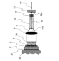
- FIG. 1 shows a configuration example of the laser apparatus of the first embodiment.
- Reference numeral 1 denotes an array element (semiconductor laser light source) in which a plurality of vertical cavity surface emitting lasers (VCSEL) are arranged along a two-dimensional matrix on one plane.
- the submount 2 is further mounted on a copper heat sink 3.
- the heat sink 3 is screwed and fixed to the chassis 20 with a highly heat conductive sheet 21 interposed therebetween.
- the VCSEL array element 1 is not provided with an electronic cooling device, and is not provided with a water-cooling cooling device.
- the array element 1 of the VCSEL is kept at 80 ° C. or less by transferring heat to the chassis 20. If necessary, the VCSEL array element 1 can be kept at 80 ° C. or lower by providing a simple cooling fan. Further, the VCSEL array element 1 can be kept at 20 ° C. or higher by using it together with a simple heating device.
- the array element 1 of the VCSEL has a semiconductor multilayer film formed on both sides of a semiconductor active layer mainly composed of GaAs, and the oscillation center wavelength of the array element 1 is determined by the band gap of GaAs and the reflection characteristics of the semiconductor multilayer film.
- a VCSEL having a temperature dependence of the oscillation center wavelength of 0.07 nm / ° C. and an oscillation center wavelength of 204.0 ° C. at 804.0 to 805.5 nm was selected.
- the array element 1 includes a plurality of light emitting points, and semiconductor laser light is emitted from each light emitting point.
- the semiconductor laser light emitted from each light emitting point is collimated by a common collimating lens 5 and is collected by a condensing lens 6 with an Nd: YAG rod 10 (Nd concentration is 1.1 at%, outer diameter is 5 mm, The light is condensed on the end face having a length of 4 mm.
- YAG rod 10 On the central optical axis 13 of the Nd: YAG rod 10, Cr: YAG saturable absorber 11 (Cr 4+ : YAG, outer diameter is 5 mm, length is 3 mm, initial transmittance at 1064 nm is 30%), and made by BK7 Flat output mirrors 12 are arranged.
- a coating film having a transmittance of 99% or more with respect to a wavelength of 803 to 810 nm is formed on both end faces of the lenses 5 and 6.
- the semiconductor laser beam condensed by the condenser lens 6 is incident on the left end face of the Nd: YAG rod 10.
- a coating film 10a having a reflectance of 99.7% or more with respect to 1064 nm (the wavelength of pulsed laser light described later) and a transmittance of 95% or more with respect to 803 to 810 nm is formed on the incident end face. ing. On the end face of the output mirror 12, a coating film 12a having a reflectance of 50% with respect to a wavelength of 1064 nm is formed. A resonator for 1064 nm is formed by the coating films 10a and 12a. A coating film having a transmittance of 99% or more with respect to 1064 nm is formed on the right end face of the Nd: YAG rod 10, both end faces of Cr: YAG 11, and the right end face of the output mirror 12.
- the efficiency is increased by reducing the light loss of the entire device.
- the semiconductor laser light condensed by the condenser lens 6 is incident on the left end face of the Nd: YAG rod 10, the semiconductor laser light is absorbed by the Nd: YAG rod 10 and the Nd: YAG rod 10 is excited. .
- the pulse laser beam 14 is emitted from the output mirror 12 to the outside of the resonator.
- the pulsed laser light has a high energy density and ignites the fuel supplied into the engine.
- FIG. 2 shows a configuration example of the laser apparatus of the second embodiment.
- Reference numeral 1 is a VCSEL array element, in which a plurality of light emitting points are arranged along a two-dimensional matrix, and an oscillation center wavelength at 20 ° C. is selected from 804.0 to 805.5 nm.
- Reference numeral 30 is a microlens array in which microlenses for collimating semiconductor laser light emitted from the light emitting points of the array element 1 of the VCSEL are arranged along a two-dimensional matrix.
- the microlens array 30 has a plurality of microlenses formed on one side of a glass substrate.
- the arrangement positions of the light emitting points coincide with the arrangement positions of the microlenses, and the semiconductor laser light emitted from one light emitting point enters each microlens.
- the microlens array 30 is arranged at a position closer to the array element 1 than a position where semiconductor laser beams from two adjacent light emitting points overlap. According to the microlens array 30, it is possible to reduce the condensing diameter of the excitation light in the Nd: YAG rod 10 as compared with the case where the single lens 5 shown in FIG. The threshold value can be lowered and the energy density of the pulsed laser beam can be increased.
- the distance can be narrowed for a long time, the overlap with the solid laser beam can be increased, and the excitation efficiency and the oscillation light rate can be increased.
- a coating having a transmittance of 99% or more with respect to semiconductor laser light having a wavelength of 803 to 810 nm is formed.
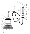
- FIG. 3 shows a configuration example of the laser apparatus of the third embodiment. Only the differences from the second embodiment will be described below.
- the semiconductor laser light emitted from the semiconductor laser light source is guided to the solid laser medium 51 using the optical fiber 40. Further, a composite rod 50 in which a polycrystalline Nd: YAG rod 51 and a polycrystalline Cr: YAG rod 52 are integrated is used.
- the semiconductor laser light is condensed on the end face of the optical fiber 40 by the condenser lens 6.
- the core diameter of the optical fiber 40 is 0.8 mm, the NA is 0.22, and the length is 3 m.
- the semiconductor laser light emitted from the other end face of the optical fiber 40 is collimated by the lens 41 and then condensed on the end face of the composite rod 50 by the condenser lens 42.
- the composite rod 50 is obtained by integrating a polycrystalline Cr: YAG rod 52 with a polycrystalline Nd: YAG rod 51.
- the polycrystalline Nd: YAG rod 51 is a kind of ceramic and is manufactured by firing.
- the polycrystalline Cr: YAG rod 52 is also a kind of ceramic and is manufactured by firing. When firing the Cr: YAG rod 52, the Nd: YAG rod 51 and the Cr: YAG rod 52 are integrated.
- the Nd concentration of the Nd: YAG rod 51 is 1.5 at%, the outer shape is 5 mm, and the length is 4 mm.
- Cr 4+ is added to the Cr: YAG rod 52, the initial transmittance is 30%, the outer shape is 5 mm, and the length is 3 mm.
- the left end surface (Nd: non-joint surface of YAG rod 51) and the right end surface (Cr: YAG rod 52 non-joint surface) of composite rod 50 are polished to a parallel plane with high accuracy.
- a coating film 50a having a reflectance of 99.7% or more with respect to 1064 nm and a transmittance of 95% or more with respect to 803 to 810 nm is formed on the non-joint surface of the Cr: YAG rod 52.
- a coating film 50b having a reflectance of 50% with respect to 1064 nm is formed on the non-joint surface of the Cr: YAG rod 52.
- a resonator for 1064 nm is formed by the coating films 50a and 50b, and the pulsed laser light 14 is emitted from the coating film 50b to the outside of the resonator.
- the Nd concentration of the polycrystalline Nd: YAG rod 51 can be increased to 2.0 at%, and when it is increased, the effective absorption coefficient can be increased as a whole (over a wavelength of 803 to 810 nm).
- FIG. 4 shows a configuration example of the laser device of the fourth embodiment. Only the differences from the third embodiment will be described below.
- an external mirror 31 is provided outside the array element 1 of the VCSEL.
- a microlens array is integrated with the external mirror 31.
- the external mirror 31 is made of synthetic quartz, and a dielectric reflection film having a reflectivity of 90% with respect to a wavelength of 803 to 810 nm is formed on the surface of the VCSEL array element 1 side, and a microscopic surface is formed on the opposite surface.
- a lens array is formed.
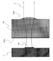
- FIG. 5 illustrates the positional relationship and functions of the light emitting point 1a, the external mirror 31, and the microlens 31b.
- a reflective film 31a is formed on the surface of the external mirror 31 on the array element 1 side.
- the reflective film 31a is parallel to the reflective film formed in the VCSEL, and the reflective film 31a and the reflective film built in the VCSEL constitute a resonator.
- the length of the resonator is significantly longer than when the resonator is configured by two reflective films in the VCSEL. The radiation angle of the semiconductor laser light emitted from the semiconductor laser light source is reduced, and the beam condensing property is improved.
- the emitted semiconductor laser light propagates through the external mirror 31, reaches the microlens 31b, and is collimated by the microlens 31b.
- the numbers and positions of the light emitting points 1a and the microlenses 31b correspond to 1: 1. 4 and 5 are the same as those in FIG. 3 in that each light emitting point is collimated. However, since the resonance length is longer than in FIG. The beam diameter after being focused by 6 is reduced, and semiconductor laser light can be introduced into a fiber having a thinner core. In the case of FIG.
- a reflective film is formed on both sides of a semiconductor active layer in the VCSEL, a resonator is formed by two reflective films in the VCSEL, and a reflective film 31a outside the VCSEL and a reflective film in the VCSEL (active A resonator can be formed by a reflective film located on the opposite side of the reflective film 31a as viewed from the layer.
- the former resonator can regulate the oscillation wavelength of the semiconductor laser light, and the latter resonator can regulate the radiation angle of the semiconductor laser light.
- the temperature dependence of the oscillation center wavelength can be suppressed to 0.07 nm / ° C. or less while using an external mirror.
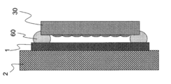
- FIG. 6 shows a structure for fixing the microlens array 30 shown in FIG. 2 to the array element 1 of the VCSEL.
- the microlens array 30 is aligned so as to be opposed to each light emitting point position of the array element 1 (that is, the light emitting point of the VCSEL and the optical axis position of the microlens are aligned), and the distance between them is the semiconductor after passing through the microlens.
- a small amount of ultraviolet (UV) curable resin adhesive 60 is inserted into three corners between the array element 1 and the microlens array 30 and irradiated with UV light.
- UV ultraviolet
- the microlens array 30 is fixed to the array element 1 of the VCSEL.
- a microlens array in which a microlens having a focal length of 0.1 mm is formed is fixed at a position about 0.1 mm away from the array element 1.
- an ultraviolet curable resin adhesive having a shrinkage rate of 2% or less by UV irradiation is used, it is possible to avoid the resin from shrinking during curing and changing the distance between the array element 1 of the VCSEL and the microlens array 30.
- UV curable adhesives with a shrinkage rate of 2% or less use, for example, 3555 from EMI, NT-01UV from NITTO DENKO, NOA61 from NORLAND, or AT4291F or AT9290F from NTT Advanced Technology Can do.
- the microlens array 30 is directly fixed to the semiconductor substrate of the array element 1 with an ultraviolet curable resin as in this embodiment, the positional shift with respect to the temperature change is only the influence of the temperature expansion and contraction of the adhesive 60, and the submount 2 and others Therefore, stable operation can be obtained over a wide temperature range. Further, since no special base, holder, or fixing space for fixing the microlens array 30 is required, the number of parts is reduced, and the cost can be reduced and the size can be reduced.
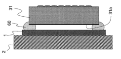
- FIG. 7 shows a structure for fixing the external mirror 31 with the microlens array shown in FIGS. 4 and 5 to the array element 1. Also in the embodiment of FIG. 7, the external mirror 31 and the array element 1 are fixed by the ultraviolet curable resin adhesive 60.
- FIG. 8 The left side of FIG. 8 shows a photograph of the array element 1 before fixing the microlens array 30, and the right side shows a photograph after fixing the microlens array 30.
- an adhesive is inserted into four corners of a 5 mm square microlens array 30, and the semiconductor substrate constituting the array element 1 and the microlens array 30 are fixed.
- FIG. 9 shows a configuration example of the laser apparatus of the fifth embodiment. Only the differences from the fourth embodiment shown in FIG. 4 will be described below.
- a concave surface having a radius of 1 mm is processed on the non-bonding end face (pulse laser light emission surface) of Cr: YAG, and a coating film 55b having a reflectance of 50% with respect to light having a wavelength of 1064 nm is formed.
- 55a and 55b form a resonator 55 for 1064 nm.
- the center point of the concave surface is on the central optical axis 13 of Nd: YAG51.
- the pulse laser beam 14 is radiated to the outside of the resonator from the end face where the coating film 55b is formed.
- a concave surface is formed on the non-bonded end surface of Cr: YAG (pulse laser beam radiation surface), the laser beam does not concentrate at the center of the beam, and damage to the solid laser medium and output mirror is unlikely to occur.
- the radius of the concave surface is preferably in the range of 0.5 to 2 mm.
- the present invention is not limited to the above-described embodiments, and can be variously modified with respect to the configurations illustrated in FIGS. 1 to 9 as a final form that operates integrally as a solid-state laser module.
- various modifications can be made to individual part shapes, types, and reflectance of the coating film, and these are not excluded from the scope of the present invention.
- the condensing lens as the excitation optical system is appropriately selected from the core diameter of the semiconductor laser element for excitation or the optical fiber and the necessary condensing beam diameter.
- One condenser lens may be arranged, or a plurality of condenser lenses may be arranged in series.
- Cr YAG is used as the optical switch element in the laser resonator, but Co: Spinal, V: YAG, or SAM which is a semiconductor material may be used.
- An active Q switch element, a polarization control element, a lens, or the like may be inserted.
- Nd YAG may be used.
- Appropriate optical elements according to the required functions can be inserted into the resonator in the required number and in the required order.
- the material of the submount 2 is not limited to SiC, and metals and ceramics having a high thermal conductivity close to that of the VCSEL array element 1, such as CuW, diamond, BeO, and AlN, can be applied.
- the material of the heat sink 3 is not limited to copper, and a metal or ceramic with high thermal conductivity such as CuW, aluminum, or AlN can be used.
- a metal or ceramic with high thermal conductivity such as CuW, aluminum, or AlN
- the highly heat-conductive sheet 21 for example, a graphite sheet manufactured by Panasonic Device Co., Ltd., a thermostar manufactured by Takeuchi Kogyo Co., Ltd., a heat conductive phase change sheet manufactured by Shin-Etsu Chemical Co., Ltd., a heat-dissipating silicone rubber made by Shin-Etsu Silicone, etc. Can do.
- the chassis 20 may be, for example, a metal body of an automobile, a housing of a laser device, or a wall of a building.
- any chassis may be used as long as the heat generated by the semiconductor laser element has a heat capacity that can be exhausted.
- this invention is not limited to the said Example, A various deformation
- the technical elements described in this specification or the drawings exhibit technical usefulness alone or in various combinations, and are not limited to the combinations described in the claims at the time of filing.
- the technology illustrated in the present specification or the drawings achieves a plurality of objects at the same time, and has technical utility by achieving one of the objects.
- VCSEL Vertical cavity surface emitting laser
- the temperature is adjusted to a temperature at which semiconductor laser light having a wavelength of 808 nm is emitted.
Landscapes
- Physics & Mathematics (AREA)
- Engineering & Computer Science (AREA)
- Electromagnetism (AREA)
- Optics & Photonics (AREA)
- General Physics & Mathematics (AREA)
- Condensed Matter Physics & Semiconductors (AREA)
- Chemical & Material Sciences (AREA)
- Combustion & Propulsion (AREA)
- Mechanical Engineering (AREA)
- General Engineering & Computer Science (AREA)
- Plasma & Fusion (AREA)
- Semiconductor Lasers (AREA)
- Lasers (AREA)
- Optical Couplings Of Light Guides (AREA)
Abstract
【課題】周囲温度が20~80℃の全範囲においてパルスレーザー光を放射する上記レーザー装置を提供する。 【解決手段】半導体レーザー光源が放射した半導体レーザー光で励起された固体レーザー媒質が放射するパルスレーザー光でエンジンに供給された燃料に点火する装置を実現するには、20~80℃の全範囲においてパルスレーザ光を放射する必要がある。現状の上記レーザー装置では動作温度範囲が不十分である。そこで固体レーザー媒質に、ネオジムを含有するイットリウム・アルミニウム・ガーネットを選択し、半導体レーザー光源に、活性層の両側に多層膜が形成されている垂直共振器面発光レーザー素子が2次元に配列されたアレイ素子を備え、20℃における発振中心波長が804.0~805.5nmであり、発振中心波長の温度依存性が0.07nm/℃以下のものを選択する。
Description
この明細書では、半導体レーザー光源と固体レーザー装置を組み合わせた装置を開示する。この組み合わせ装置では、半導体レーザー光源が半導体レーザー光を放射し、その半導体レーザー光で励起された固体レーザー装置が固体レーザー光を放射する。本明細書では、半導体レーザー光源と固体レーザー装置を備えており、半導体レーザー光源から放射された半導体レーザー光が固体レーザー媒質に入射し、半導体レーザー光で励起された固体レーザー媒質が固体レーザー光を放射する装置の全体を「半導体レーザー光で励起される固体レーザー装置」という。以下では簡単化のために、単に「レーザー装置」と省略する。
本明細書では、上記レーザー装置の動作温度範囲を広げる技術を開示する。特に、上記レーザー装置によって、エンジンに供給された燃料に点火する装置を実現するのに必要な動作温度範囲に広げる技術を開示する。
本明細書では、半導体レーザー光源が放射するレーザー光を半導体レーザー光といい、固体レーザー媒質が放射するレーザー光を固体レーザー光という。両者はともにレーザー光である。
本明細書では、上記レーザー装置の動作温度範囲を広げる技術を開示する。特に、上記レーザー装置によって、エンジンに供給された燃料に点火する装置を実現するのに必要な動作温度範囲に広げる技術を開示する。
本明細書では、半導体レーザー光源が放射するレーザー光を半導体レーザー光といい、固体レーザー媒質が放射するレーザー光を固体レーザー光という。両者はともにレーザー光である。
図15に、非特許文献1に開示されている上記レーザー装置の構成を示す。図15において、参照番号101は垂直共振器面発光レーザー素子(VCSEL)の複数個が2次元の行列に沿って配置されているアレイ素子(半導体レーザー光源の一例)を示し、参照番号105はコリメートレンズを示し、参照番号106は集光レンズを示し、参照番号110はネオジムを含有するイットリウム・アルミニウム・ガーネット(Nd:YAG)を示し、参照番号111はクロムを含有するイットリウム・アルミニウム・ガーネット(Cr:YAG)を示し、参照番号115はブリュースター板を示し、参照番号112は出力ミラーを示している。Nd:YAG110はロッド形状であり、半導体レーザー光が入射する側の端面に、808nmに対しては高透過率であり1064nmに対しては高反射率の誘電体コート膜110aが形成されている。出力ミラー112は、1064nmに対して90%の反射率を持つ膜112aを備えている。Nd:YAG110は、半導体レーザー光に照射されると励起して固体レーザー光を発振する固体レーザー媒質である。誘電体コート膜110aと膜112aの間に位置する光学装置によって、Nd:YAG固体レーザー共振器が形成されている。
アレイ素子101は、波長808nmに制御された半導体レーザー光を放射する。その半導体レーザー光は、2枚のレンズ105,106によりNd:YAG110の端面に集光される。Nd:YAG110の端面に集光された半導体レーザー光は、Nd:YAG110内に入射して吸収される。Nd:YAG110は固体レーザー媒質となる。共振器内に挿入されているCr:YAG111は、受動Qスイッチとして動作し、パルスレーザー光を放射させる。ブリュースター板115は、パルスレーザー光を直線偏光に制御する。
アレイ素子101を調温するために、アレイ素子101をダイヤモンド製のヒートスプレッダーにマウントし、そのヒートスプレッダーを銅製のヒートシンクにマウントし、そのヒートシンクを電子冷却装置で冷却する構成がとられる。アレイ素子101は、電子冷却装置によって、アレイ素子101が放射する半導体レーザー光の波長が808nmとなる温度に調温される。
図16は、非特許文献2に開示されている半導体レーザー光源を示している。この半導体レーザー光源は、ファイバーレーザー140を励起する半導体レーザー光を放射する。参照番号101はVCSELのアレイ素子を示し、参照番号130はVCSELのアレイ素子101の各発光点から放射される半導体レーザー光を個々にコリメートするためのマイクロレンズのアレイを示し、参照番号106は半導体レーザー光107をファイバー140の端面に集光するための集光レンズを示している。
アレイ素子101は、波長は976nmの半導体レーザー光を放射する。アレイ素子101を調温するために、アレイ素子101をダイヤモンド製のサブマウント102にマウントし、サブマウント102を銅製の水冷式マイクロチャンネルヒートシンクにマウントして温度制御される。アレイ素子101は、放射する半導体レーザー光の波長が976nmとなる温度に調温される。
図17は、非特許文献3に開示されている半導体レーザー光源を示している。この半導体レーザー光源は、ファイバーレーザー140を励起する半導体レーザー光を放射する。参照番号101は垂直共振器面発光レーザー(VCSEL)のアレイ素子を示し、参照番号131は外部ミラーを示し、参照番号130はアレイ素子101の各発光点からの半導体レーザー光を個々にコリメートするマイクロレンズのアレイを示し、参照番号106は集光レンズを示している。アレイ素子101は、波長976nmの半導体レーザー光を放射する。VCSELの外部にミラー131を設けることで、VCSELのアレイ素子101の共振器長を実効的に長くすることができ、これによりアレイ素子101から放射される半導体レーザー光の放射角が狭くなり、輝度が上がる。ミラーをVCSEL内に内蔵する図16の構成に比べ、コアの小さな光ファイバーに効率よく半導体レーザー光を入射させることができる。
VCSELのアレイ101を調温するために、アレイ素子101をダイヤモンド製のサブマウント102にマウントし、そのサブマウント102を銅のブロックにマウントして冷却する。アレイ素子101は、アレイ素子101が放射する半導体レーザー光の波長が976nmとなる温度に調温される。
VCSELのアレイ101を調温するために、アレイ素子101をダイヤモンド製のサブマウント102にマウントし、そのサブマウント102を銅のブロックにマウントして冷却する。アレイ素子101は、アレイ素子101が放射する半導体レーザー光の波長が976nmとなる温度に調温される。
Solid State Lasers XXI, Proc. of SPIE Vol. 8235 82350M (2012)
High-Power Diode Laser Technology and Applications VI, Proc. of SPIE Vol. 6876 68760D (2008)
Vertical-Cavity Surface-Emitting Lasers XIV, Proc. of SPIE Vol. 7615 76150F (2010)
近年、上記レーザー装置の性能向上とともに、理化学用あるいは工業用への普及が進んでいるが、さらに産業用、民生用の広い応用分野に普及を進めるためには、上記レーザー装置の動作温度範囲の拡大が課題となっている。例えば自動車に搭載する場合、20℃から80℃までの温度範囲で安定的に動作することが要求される。自動車が使用される環境温度は、上記の温度範囲より広いが、上記レーザー装置を冷却するのに比して上記レーザー装置を加熱するのには少ない電力で済むこと、上記レーザー装置に通電すると装置自体が発熱すること、冷却ファンで上記レーザー装置を空冷する程度の空冷装置を設けることが可能であるといった諸事情から、上記レーザー装置が20℃から80℃までの温度範囲で安定的に動作することができれば、上記レーザー装置を車載することが可能となる。
半導体レーザー光源の発振中心波長には、温度依存性が存在する。半導体レーザー光源の発振中心波長は、一義的には半導体活性層のバンドギャップで決定される。ところが、そのバンドギャップが温度に依存して変化するために、半導体レーザー光源の発振中心波長は温度に依存して変化する。通常の半導体レーザー光源の場合、環境温度が1℃上昇すると発振中心波長が0.3nmだけ長くなる。その一方、固体レーザー媒質の吸収帯は比較的に狭い。Nd:YAGの場合、図10に示すように、807.0~809.5nmに強い吸収帯Aがある。このことは、動作温度が8℃だけ変化すると、半導体レーザー光源の発振中心波長が、固体レーザー媒質の吸収帯Aの最短波長807.0nmから最長波長809.5nmにまで変化してしまうことを意味する。従来の上記レーザー装置の動作温度範囲は8℃にすぎない。
そこで、従来の上記レーザー装置の場合、特定の動作温度における半導体レーザー光の波長が上記吸収帯Aなかでも最大吸収係数となる808nmの近傍となる半導体レーザー光源を選択し、かつ半導体レーザー光源をその動作温度に維持する電子冷却装置あるいは水冷式冷却装置を併用している。
上記レーザー装置を車載するためには空冷する程度では足りず、電子冷却装置あるいは水冷式冷却装置が必要とされるとすると、上記レーザー装置を車載するのが困難となる。上記レーザー装置がもたらすメリットを享受できる機会が大幅に減少してしまう。
本明細書では、電子冷却装置あるいは水冷式冷却装置を必要とせず、簡単な加熱装置あるいは簡単な空冷装置程度と併用することで車載することが可能となる上記レーザー装置を開示する。
特に、上記レーザー装置が放射するパルスレーザー光でエンジンに供給された燃料に点火する点火装置を実現する技術を開示する。
本明細書では、20℃から80℃までの温度範囲で安定的に動作する上記レーザー装置が得られれば、電子冷却装置あるいは水冷式冷却装置を併用する必要がなくなり、簡単な加熱装置あるいは簡単な空冷装置程度と併用することで車載することが可能となるという知見に基づいて創作された、上記レーザー装置あるいはそれを利用した点火装置を開示する。
特に、上記レーザー装置が放射するパルスレーザー光でエンジンに供給された燃料に点火する点火装置を実現する技術を開示する。
本明細書では、20℃から80℃までの温度範囲で安定的に動作する上記レーザー装置が得られれば、電子冷却装置あるいは水冷式冷却装置を併用する必要がなくなり、簡単な加熱装置あるいは簡単な空冷装置程度と併用することで車載することが可能となるという知見に基づいて創作された、上記レーザー装置あるいはそれを利用した点火装置を開示する。
本明細書に記載の技術では、次の2つの知見を組み合わせて用いる。
(第1知見)半導体レーザー光源の発振中心波長は、一義的には半導体活性層のバンドギャップで決定されるが、それだけでは決まらず、共振器を構成するミラーの反射特性の影響も受ける。そこで、半導体活性層の両側に配置するミラーに半導体多層膜を利用し、分布ブラッグ反射を利用するVCSELが開発されている。このVCSELによると、発振中心波長の温度依存性が、0.07nm/℃まで低下する。例えば、Princeton Optronics, Inc. (1 Electronics Drive, Mercerville, New Jersey 08619, USA)社が提供するVCSELの発振中心波長の温度依存性は0.07nm/℃である。
(第2知見)従来の上記レーザー装置は、図10に示した吸収帯Aを利用するが、実際には、それに隣接する波長帯Bでも吸収能力を備えており、吸収帯Aと吸収帯Bの全体を利用することができる。吸収帯Bでの吸収係数は吸収帯Aでの吸収係数より低いので今まで使われなかったが、固体レーザー光を発振させることは可能である。
(第1知見)半導体レーザー光源の発振中心波長は、一義的には半導体活性層のバンドギャップで決定されるが、それだけでは決まらず、共振器を構成するミラーの反射特性の影響も受ける。そこで、半導体活性層の両側に配置するミラーに半導体多層膜を利用し、分布ブラッグ反射を利用するVCSELが開発されている。このVCSELによると、発振中心波長の温度依存性が、0.07nm/℃まで低下する。例えば、Princeton Optronics, Inc. (1 Electronics Drive, Mercerville, New Jersey 08619, USA)社が提供するVCSELの発振中心波長の温度依存性は0.07nm/℃である。
(第2知見)従来の上記レーザー装置は、図10に示した吸収帯Aを利用するが、実際には、それに隣接する波長帯Bでも吸収能力を備えており、吸収帯Aと吸収帯Bの全体を利用することができる。吸収帯Bでの吸収係数は吸収帯Aでの吸収係数より低いので今まで使われなかったが、固体レーザー光を発振させることは可能である。
吸収帯Aと吸収帯Bの全体を利用すると、吸収帯が803.0~809.5nmに拡大する。すなわち、6.5nmの波長幅を持つ。前記した0.07nm/℃の温度依存性を持つ半導体レーザー光源と組み合わせて用いると、90℃以上の動作温度範囲を確保することが可能となる。
本明細書で開示する上記レーザー装置は、上記考察と波長決定実験によって得られたものであり、
(1)固体レーザー媒質に、ネオジムを含有するイットリウム・アルミニウム・ガーネット(Nd:YAG)を用いる。
(2)半導体レーザー光源に、活性層の両側に多層膜が形成されている垂直共振器面発光レーザー素子(VCSEL)が2次元に配列されたアレイ光源を用いる。特に、20℃における発振中心波長が804.0~805.5nmであり、発振中心波長の温度依存性が0.07nm/℃以下である半導体レーザー光源を用いる。
(1)固体レーザー媒質に、ネオジムを含有するイットリウム・アルミニウム・ガーネット(Nd:YAG)を用いる。
(2)半導体レーザー光源に、活性層の両側に多層膜が形成されている垂直共振器面発光レーザー素子(VCSEL)が2次元に配列されたアレイ光源を用いる。特に、20℃における発振中心波長が804.0~805.5nmであり、発振中心波長の温度依存性が0.07nm/℃以下である半導体レーザー光源を用いる。
図11から図13の縦軸は、20℃において半導体レーザー光源から放射された励起光エネルギーと、固体レーザー媒質内で吸収されたエネルギーの比(前者を1としたときの後者の値)を示す。半導体レーザー光源に加える電力量は、環境温度によらずに一定に保った。環境温度が変化すると、半導体レーザー光源から放射される半導体レーザー光の波長が変化し(従って図10に示した吸収係数が変化する)、さらに半導体レーザー光のエネルギーも変化する。縦軸は、2つの効果を加味した有効吸収割合を示している。以下では便宜的に、有効吸収係数という。図11から図13の縦軸は、長さが4mmのNd:YAGの有効吸収係数の温度依存性の測定結果を示している。
図11は、20℃における発振中心波長が803.0nmである半導体レーザー光源を用いた場合と、803.5nmの半導体レーザー光源を用いた場合を示す。図11の場合、環境温度が低い場合における半導体レーザー光の波長が吸収帯Bの最短波長に比しても短すぎ、環境温度が低い場合における有効吸収係数が低下してしまう。
図13は、20℃における発振中心波長が806.0nmである半導体レーザー光源を用いた場合と、806.5nmの半導体レーザー光源を用いた場合を示している。図13の場合、環境温度が高い場合における半導体レーザー光の波長が吸収帯Aの最長波長に比しても長すぎ、環境温度が高い場合における有効吸収係数が低下してしまう。
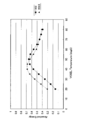
図12は、20℃における発振中心波長が804.0nm、804.5nm、805.0nm、805.5nmの半導体レーザー光源を用いた場合の有効吸収係数を示す。図12の場合、環境温度が低い場合にも波長が短すぎず、環境温度が高い場合にも波長が長すぎず、20℃~80℃の全温度範囲において、40%以上の有効吸収係数を確保できることがわかる。
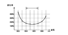
図14は、図11から図13に示した有効吸収係数から「20~80℃内の最高有効吸収係数/20~80℃内の最少有効吸収係数」の値を求めた結果を示している。20℃における発振中心波長が804.0~805.5nmの範囲内にあると、前記した比の値が2.0未満に抑えられることがわかる。
図11は、20℃における発振中心波長が803.0nmである半導体レーザー光源を用いた場合と、803.5nmの半導体レーザー光源を用いた場合を示す。図11の場合、環境温度が低い場合における半導体レーザー光の波長が吸収帯Bの最短波長に比しても短すぎ、環境温度が低い場合における有効吸収係数が低下してしまう。
図13は、20℃における発振中心波長が806.0nmである半導体レーザー光源を用いた場合と、806.5nmの半導体レーザー光源を用いた場合を示している。図13の場合、環境温度が高い場合における半導体レーザー光の波長が吸収帯Aの最長波長に比しても長すぎ、環境温度が高い場合における有効吸収係数が低下してしまう。
図12は、20℃における発振中心波長が804.0nm、804.5nm、805.0nm、805.5nmの半導体レーザー光源を用いた場合の有効吸収係数を示す。図12の場合、環境温度が低い場合にも波長が短すぎず、環境温度が高い場合にも波長が長すぎず、20℃~80℃の全温度範囲において、40%以上の有効吸収係数を確保できることがわかる。
図14は、図11から図13に示した有効吸収係数から「20~80℃内の最高有効吸収係数/20~80℃内の最少有効吸収係数」の値を求めた結果を示している。20℃における発振中心波長が804.0~805.5nmの範囲内にあると、前記した比の値が2.0未満に抑えられることがわかる。
上記レーザー装置を車載する場合、20~80℃の全温度範囲において40%以上の有効吸収係数を確保でき、かつ、20~80℃内の最高有効吸収係数/20~80℃内の最少有効吸収係数の比の値が2.0以下であれば、電子冷却装置あるいは水冷式冷却装置を併用する必要がなく、簡単な加熱装置あるいは簡単な空冷式冷却装置または簡単な出力調整回路と併用する程度の対策によって、車載することが可能となることが確認されている。本明細書に開示されているレーザー装置(正確には半導体レーザー光で励起する固体レーザー装置)によると、実用的な意味で車載することが可能となる。固体レーザー媒質が放射するパルスレーザー光で燃料に点火する点火装置を車載することが可能となる。
本明細書に開示する技術では、吸収係数の低い吸収帯Bをも利用するために、Nd:YAGの吸収係数を上げる技術と併用することが好ましい。吸収係数を向上させるためにはNd濃度を上げることが望ましいが、単結晶YAGの場合にはNd濃度が1.1at%を超えるとレーザー特性が著しく低下することが知られている、これに対し最近実用化された多結晶YAGの場合、Nd濃度を2.0at%程度にまで上げても、レーザー特性の低下が少ないことが知られている。
そのために、固体レーザー媒質に、1.1~2.0at%のネオジムを含有する多結晶のNd:YAGを用いるのが有効である。
そのために、固体レーザー媒質に、1.1~2.0at%のネオジムを含有する多結晶のNd:YAGを用いるのが有効である。
多結晶のNd:YAGや多結晶のCr:YAGは、焼結して製造することができ、セラミックの製造方法を適用することができる。セラミックの製造方法を適用することで、Nd:YAGとCr:YAGが一体化されているロッドを簡便に製造することができる。Nd:YAGとCr:YAGが一体化されているロッドを用いると、パルスレーザー光放射装置を構成する光学素子の数を減らすことができ、パルスレーザー光放射装置を小型化することができ、振動等に強いパルスレーザー光放射装置を実現することができる。
Nd:YAGの端面にCr:YAGが接合されている光学素子を利用する場合、Nd:YAGの一方の端面とCr:YAGの一方の端面を接合し、Nd:YAGの非接合端面とCr:YAGの非接合面を平行とする。Nd:YAGの非接合端面に半導体レーザー光が入射すると、Cr:YAGの非接合面からパルスレーザー光が放射する関係を得ることができる。
Nd:YAGの端面にCr:YAGが接合されている光学素子を利用する場合、Nd:YAGの一方の端面とCr:YAGの一方の端面を接合し、Nd:YAGの非接合端面とCr:YAGの非接合面を平行とする。Nd:YAGの非接合端面に半導体レーザー光が入射すると、Cr:YAGの非接合面からパルスレーザー光が放射する関係を得ることができる。
固体レーザー共振器の出力ミラーに凹面が形成されていると、固体レーザー光がビーム中央に集中せず、レーザー媒質や出力ミラーにダメージが発生しにくくなり、動作が安定する。
そこで、Cr:YAGの非接合面に、0.5~2mmの半径の凹面が形成されていることが好ましい。
この場合、凹面の中心がNd:YAGの中心光軸上にあることが好ましい。
そこで、Cr:YAGの非接合面に、0.5~2mmの半径の凹面が形成されていることが好ましい。
この場合、凹面の中心がNd:YAGの中心光軸上にあることが好ましい。
半導体レーザー光源と固体レーザー媒質の間を光ファイバーで接続することができる。光ファイバーを利用すると、半導体レーザー光源と固体レーザー媒質を離して配置することができる。固定レーザー媒質の特性は温度に依存して変化しづらいのに対し、半導体レーザー光源の特性は温度に依存して変化しやすい。そこで、例えば温度が大きく変化するエンジンルーム内に固体レーザー媒質を配置し、温度変化幅が比較的小さな車室内に半導体レーザー光源を配置し、両者を光ファイバーで接続するといった技術が有効である。
VCSELは複数の発光点を備えており、図16と図17に示したように、各発光点から放射された半導体レーザー光をマイクロレンズでコリメートすると、半導体レーザー光を小さな範囲に集光することができる。また、図17に示したように、半導体レーザー光の共振器を構成するミラーをVCSELの外部に設けると、半導体レーザー光の放射角度範囲を狭くすることができる。上記のマイクロレンズアレイと上記のミラーを一体に形成すると、必要な部品点数を減らすことができる。
そこで、VCSELの各発光点から放射された半導体レーザー光を個々にコリメートするマイクロレンズが2次元に配列されたマイクロレンズアレイと、反射膜が一体に形成されているミラー兼マイクロレンズアレイを、VCSELとNd:YAGの間に配置する構造がとりえる。光ファイバーを利用する場合には、ミラー兼マイクロレンズアレイをVCSELと光ファイバーの間に配置する構造がとりえる。
そこで、VCSELの各発光点から放射された半導体レーザー光を個々にコリメートするマイクロレンズが2次元に配列されたマイクロレンズアレイと、反射膜が一体に形成されているミラー兼マイクロレンズアレイを、VCSELとNd:YAGの間に配置する構造がとりえる。光ファイバーを利用する場合には、ミラー兼マイクロレンズアレイをVCSELと光ファイバーの間に配置する構造がとりえる。
マイクロレンズアレイを用いる場合、硬化収縮率が2%以下の紫外線硬化樹脂によってマイクロレンズアレイとVCSELを固定することが好ましい。硬化収縮率が2%以下の紫外線硬化樹脂を用いると、樹脂が硬化して収縮する際に、VCSELとマイクロレンズの距離が変化してしまうことによる悪影響を避けることができる。
本明細書に記載の上記レーザー装置によって車載式の点火装置を実現することができるが、その用途は点火装置に限られない。動作温度範囲が広いパルスレーザー光放射装置自体が有用性を備えている。
本明細書に記載されている上記レーザー装置によると、20~80℃の全温度範囲においてパルスレーザー光を放射し、かつ、パルスレーザー光の放射エネルギーの変化幅が小さなパルスレーザー放射装置が得られる。そのために、上記レーザー装置を車載することが可能となり、上記レーザー装置によって燃料に点火する車載式点火装置を実現することができる。エンジン内での燃焼効率を高め、燃費を高め、排出ガスの無害化を図るといったことが可能となる。
以下に説明する実施例の特徴を先に列記する。
(形態1)車室内に半導体レーザー光源を配置し、エンジンルーム内に固体レーザー媒質を配置し、両者を光ファイバーで接続する。
(形態2)半導体レーザー光源に加熱装置を付加し、冷温時には20℃以上に加熱する。
(形態3)半導体レーザー光源に冷却ファンによる冷却風をあて、80℃以下に抑える。
(形態4)半導体レーザー光源には、電子冷却装置も水冷式冷却装置も付け加えられていない。
(形態1)車室内に半導体レーザー光源を配置し、エンジンルーム内に固体レーザー媒質を配置し、両者を光ファイバーで接続する。
(形態2)半導体レーザー光源に加熱装置を付加し、冷温時には20℃以上に加熱する。
(形態3)半導体レーザー光源に冷却ファンによる冷却風をあて、80℃以下に抑える。
(形態4)半導体レーザー光源には、電子冷却装置も水冷式冷却装置も付け加えられていない。
以下、実施例を詳細に説明する。図1は、第1実施例の上記レーザー装置の構成例を示している。
参照番号1は、垂直共振器面発光レーザー(VCSEL)の複数個が、1平面上において2次元の行列に沿って配置されたアレイ素子(半導体レーザー光源)であり、SiC製のサブマウント2にマウントされ、サブマウント2はさらに銅製のヒートシンク3にマウントされている。ヒートシンク3は、高熱伝導性のシート21を挟んでシャーシ20にネジ止め固定されている。VCSELのアレイ素子1には、電子冷却装置も設けられていなければ、水冷式冷却装置も設けられていない。VCSELのアレイ素子1は、シャーシ20に伝熱することで80℃以下に保たれる。必要であれば、簡単な冷却ファンを設けることによってVCSELのアレイ素子1を80℃以下に保つことができる。また、簡単な加熱装置と併用することによってVCSELのアレイ素子1を20℃以上に保つことができる。
参照番号1は、垂直共振器面発光レーザー(VCSEL)の複数個が、1平面上において2次元の行列に沿って配置されたアレイ素子(半導体レーザー光源)であり、SiC製のサブマウント2にマウントされ、サブマウント2はさらに銅製のヒートシンク3にマウントされている。ヒートシンク3は、高熱伝導性のシート21を挟んでシャーシ20にネジ止め固定されている。VCSELのアレイ素子1には、電子冷却装置も設けられていなければ、水冷式冷却装置も設けられていない。VCSELのアレイ素子1は、シャーシ20に伝熱することで80℃以下に保たれる。必要であれば、簡単な冷却ファンを設けることによってVCSELのアレイ素子1を80℃以下に保つことができる。また、簡単な加熱装置と併用することによってVCSELのアレイ素子1を20℃以上に保つことができる。
VCSELのアレイ素子1は、GaAsを主材とする半導体活性層の両側に半導体多層膜が形成されており、アレイ素子1の発振中心波長はGaAsのバンドギャップと半導体多層膜の反射特性によって決まる。本実施例では、発振中心波長の温度依存性が0.07nm/℃であり、20℃における発振中心波長が、804.0~805.5nmであるVCSELを選択した。
アレイ素子1は複数個の発光点を備えており、各発光点から半導体レーザー光が放射される。第1実施例では、各発光点から放射された半導体レーザー光が共通のコリメートレンズ5でコリメートされ、集光レンズ6でNd:YAGロッド10(Nd濃度が1.1at%、外径が5mm、長さが4mm)の端面に集光される。Nd:YAGロッド10の中心光軸13上に、Cr:YAG可飽和吸収体11(Cr4+:YAG、外径が5mm、長さが3mm、1064nmにおける初期透過率が30%)と、BK7製の平面出力ミラー12が配列されている。
レンズ5,6の両端面には、波長803~810nmに対して99%以上の透過率を有するコーティング膜が形成されている。Nd:YAGロッド10の左側の端面には、集光レンズ6で集光された半導体レーザー光が入射する。その入射端面には、1064nm(後記するパルスレーザー光の波長)に対して99.7%以上の反射率であり、803~810nmに対して95%以上の透過率を有するコーティング膜10aが形成されている。出力ミラー12の端面には、1064nmの波長に対して50%の反射率を持つコーティング膜12aが形成されている。コーティング膜10aと12aによって、1064nmに対する共振器が形成されている。Nd:YAGロッド10の右側の端面と、Cr:YAG11の両端面と、出力ミラー12の右側の端面には、1064nmに対して99%以上の透過率を有するコーティング膜が形成されており、レーザー装置全体の光の損失を低くして効率を高めている。
Nd:YAGロッド10の左側の端面に、集光レンズ6で集光された半導体レーザー光が入射すると、その半導体レーザー光はNd:YAGロッド10で吸収され、Nd:YAGロッド10が励起される。その結果、パルスレーザー光14が出力ミラー12から共振器外部に放射される。パルスレーザー光は高いエネルギー密度を備えており、エンジン内に供給された燃料に点火する。
レンズ5,6の両端面には、波長803~810nmに対して99%以上の透過率を有するコーティング膜が形成されている。Nd:YAGロッド10の左側の端面には、集光レンズ6で集光された半導体レーザー光が入射する。その入射端面には、1064nm(後記するパルスレーザー光の波長)に対して99.7%以上の反射率であり、803~810nmに対して95%以上の透過率を有するコーティング膜10aが形成されている。出力ミラー12の端面には、1064nmの波長に対して50%の反射率を持つコーティング膜12aが形成されている。コーティング膜10aと12aによって、1064nmに対する共振器が形成されている。Nd:YAGロッド10の右側の端面と、Cr:YAG11の両端面と、出力ミラー12の右側の端面には、1064nmに対して99%以上の透過率を有するコーティング膜が形成されており、レーザー装置全体の光の損失を低くして効率を高めている。
Nd:YAGロッド10の左側の端面に、集光レンズ6で集光された半導体レーザー光が入射すると、その半導体レーザー光はNd:YAGロッド10で吸収され、Nd:YAGロッド10が励起される。その結果、パルスレーザー光14が出力ミラー12から共振器外部に放射される。パルスレーザー光は高いエネルギー密度を備えており、エンジン内に供給された燃料に点火する。
(第2実施例)
図2は、第2実施例の上記レーザー装置の構成例を示している。以下では、第1実施例との相違点のみを説明し、重複説明を省略する。参照番号1は、VCSELのアレイ素子であり、複数個の発光点が2次元の行列に沿って配置されており、20℃における発振中心波長が804.0~805.5nmのものが選択されている。参照番号30は、VCSELのアレイ素子1の発光点から放射された半導体レーザー光をコリメートするマイクロレンズが2次元の行列に沿って配置されているマイクロレンズアレイである。マイクロレンズアレイ30は、ガラス基板上の片面に複数個のマイクロレンズが形成されたものである。発光点の配置位置とマイクロレンズの配置位置は一致しており、各々のマイクロレンズには1個の発光点から放射された半導体レーザー光が入射する。隣接する2個の発光点からの半導体レーザー光が重なり合う位置よりもアレイ素子1に近い位置にマイクロレンズアレイ30が配置されている。マイクロレンズアレイ30によると、図1に示した単一のレンズ5を使用する場合に比して、Nd:YAGロッド10内の励起光集光径を細くすることができるので、固体レーザーの発振閾値を下げたり、パルスレーザー光のエネルギー密度を上げたりすることができる。また長い距離絞れるので固体レーザー光との重なりを大きくでき、励起効率や発振光率を高めることもできる。マイクロレンズアレイ30の両端面には波長803~810nmの半導体レーザー光に対して99%以上の透過率を有するコーティングが形成されている。
図2は、第2実施例の上記レーザー装置の構成例を示している。以下では、第1実施例との相違点のみを説明し、重複説明を省略する。参照番号1は、VCSELのアレイ素子であり、複数個の発光点が2次元の行列に沿って配置されており、20℃における発振中心波長が804.0~805.5nmのものが選択されている。参照番号30は、VCSELのアレイ素子1の発光点から放射された半導体レーザー光をコリメートするマイクロレンズが2次元の行列に沿って配置されているマイクロレンズアレイである。マイクロレンズアレイ30は、ガラス基板上の片面に複数個のマイクロレンズが形成されたものである。発光点の配置位置とマイクロレンズの配置位置は一致しており、各々のマイクロレンズには1個の発光点から放射された半導体レーザー光が入射する。隣接する2個の発光点からの半導体レーザー光が重なり合う位置よりもアレイ素子1に近い位置にマイクロレンズアレイ30が配置されている。マイクロレンズアレイ30によると、図1に示した単一のレンズ5を使用する場合に比して、Nd:YAGロッド10内の励起光集光径を細くすることができるので、固体レーザーの発振閾値を下げたり、パルスレーザー光のエネルギー密度を上げたりすることができる。また長い距離絞れるので固体レーザー光との重なりを大きくでき、励起効率や発振光率を高めることもできる。マイクロレンズアレイ30の両端面には波長803~810nmの半導体レーザー光に対して99%以上の透過率を有するコーティングが形成されている。
(第3実施例)
図3は、第3実施例の上記レーザー装置の構成例を示している。以下では、第2実施例との相違点のみを説明する。第3実施例では、半導体レーザー光源から放射された半導体レーザー光を、光ファイバー40を利用して、固体レーザー媒質51に導く。また、多結晶Nd:YAGロッド51と多結晶Cr:YAGロッド52を一体化した複合ロッド50を用いる。
第3実施例では、半導体レーザー光が集光レンズ6によって光ファイバー40の端面に集光される。光ファイバー40のコア径は0.8mmであり、NAは0.22であり、長さは3mである。光ファイバー40の他方の端面から出射した半導体レーザー光は、レンズ41でコリメートされた後、集光レンズ42で複合ロッド50の端面に集光される。
複合ロッド50は、多結晶のNd:YAGロッド51に、多結晶のCr:YAGロッド52が一体化されたものである。多結晶のNd:YAGロッド51は、セラミックの一種であり、焼成して製造する。多結晶のCr:YAGロッド52も、セラミックの一種であり、焼成して製造する。Cr:YAGロッド52を焼成する際に、Nd:YAGロッド51とCr:YAGロッド52が一体化される。Nd:YAGロッド51のNd濃度は1.5at%であり、外形は5mmであり、長さは4mmである。Cr:YAGロッド52にはCr4+が添加されており、初期透過率は30%であり、外形は5mmであり、長さは3mmである。複合ロッド50の左側端面(Nd:YAGロッド51の非接合面)と右側端面(Cr:YAGロッド52の非接合面)は、高精度に平行平面に研磨されている。Nd:YAGロッド51の非接合面には、1064nmに対して99.7%以上の反射率をもち、803~810nmに対して95%以上の透過率を有するコーティング膜50aが形成されている。Cr:YAGロッド52の非接合面には、1064nmに対して50%の反射率を持つコーティング膜50bが形成されている。コーティング膜50a、50bによって1064nmに対する共振器を形成し、パルスレーザー光14がコーティング膜50bから共振器外部に放射される。多結晶Nd:YAGロッド51のNd濃度を2.0at%にまで濃くすることが可能であり、濃くすると有効吸収係数を全体に(803~810nmの波長にわたって)上げることができる。
図3は、第3実施例の上記レーザー装置の構成例を示している。以下では、第2実施例との相違点のみを説明する。第3実施例では、半導体レーザー光源から放射された半導体レーザー光を、光ファイバー40を利用して、固体レーザー媒質51に導く。また、多結晶Nd:YAGロッド51と多結晶Cr:YAGロッド52を一体化した複合ロッド50を用いる。
第3実施例では、半導体レーザー光が集光レンズ6によって光ファイバー40の端面に集光される。光ファイバー40のコア径は0.8mmであり、NAは0.22であり、長さは3mである。光ファイバー40の他方の端面から出射した半導体レーザー光は、レンズ41でコリメートされた後、集光レンズ42で複合ロッド50の端面に集光される。
複合ロッド50は、多結晶のNd:YAGロッド51に、多結晶のCr:YAGロッド52が一体化されたものである。多結晶のNd:YAGロッド51は、セラミックの一種であり、焼成して製造する。多結晶のCr:YAGロッド52も、セラミックの一種であり、焼成して製造する。Cr:YAGロッド52を焼成する際に、Nd:YAGロッド51とCr:YAGロッド52が一体化される。Nd:YAGロッド51のNd濃度は1.5at%であり、外形は5mmであり、長さは4mmである。Cr:YAGロッド52にはCr4+が添加されており、初期透過率は30%であり、外形は5mmであり、長さは3mmである。複合ロッド50の左側端面(Nd:YAGロッド51の非接合面)と右側端面(Cr:YAGロッド52の非接合面)は、高精度に平行平面に研磨されている。Nd:YAGロッド51の非接合面には、1064nmに対して99.7%以上の反射率をもち、803~810nmに対して95%以上の透過率を有するコーティング膜50aが形成されている。Cr:YAGロッド52の非接合面には、1064nmに対して50%の反射率を持つコーティング膜50bが形成されている。コーティング膜50a、50bによって1064nmに対する共振器を形成し、パルスレーザー光14がコーティング膜50bから共振器外部に放射される。多結晶Nd:YAGロッド51のNd濃度を2.0at%にまで濃くすることが可能であり、濃くすると有効吸収係数を全体に(803~810nmの波長にわたって)上げることができる。
(第4実施例)
図4は、第4実施例の上記レーザー装置の構成例を示している。以下では、第3実施例との相違点のみを説明する。
第4実施例では、VCSELのアレイ素子1の外側に外部ミラー31を設ける。外部ミラー31にはマイクロレンズアレイが一体化されている。外部ミラー31は合成石英製であり、VCSELのアレイ素子1の側の面に、波長803~810nmに対して90%の反射率を持つ誘電体反射膜が形成され、反対側の面にはマイクロレンズアレイが形成されている。
図5は、発光点1aと外部ミラー31とマイクロレンズ31bの位置関係と機能を説明したものである。外部ミラー31のアレイ素子1の側の面に反射膜31aが形成されている。反射膜31aは、VCSELの中に形成されている反射膜と平行であり、反射膜31aとVCSELに内蔵されている反射膜で共振器を構成する。VCSEL外の反射膜31aとVCSEL内の反射膜で共振器を構成すると、VCSEL内の2枚の反射膜で共振器を構成する場合に比して、共振器の長さが格段に長くなるため、半導体レーザー光源から放射される半導体レーザー光の放射角が小さくなり、ビームの集光性が向上する。放射された半導体レーザー光は、外部ミラー31内を伝搬してマイクロレンズ31bに至り、マイクロレンズ31bによってコリメートされる。発光点1aとマイクロレンズ31bの数と位置は、1:1に対応している。図4、図5の場合、発光点ごとにコリメ-トする点では図3と同じであるが、図3にくらべて共振長が長くて各ビームの集光性が高いために、集光レンズ6によって集光した後のビーム径は小さくなり、よりコアの細いファイバーへ半導体レーザー光を導入することができる。
図5の場合、VCSEL内の半導体活性層の両側に反射膜を形成し、VCSEL内の2枚の反射膜で共振器を形成するとともに、VCSEL外の反射膜31aとVCSEL内の反射膜(活性層から見て反射膜31aと反対側に位置する反射膜)で共振器を形成することができる。前者の共振器で半導体レーザー光の発振波長を規制し、後者の共振器で半導体レーザー光の放射角を規制することができる。外部ミラーと利用しながら、発振中心波長の温度依存性を0.07nm/℃以下に抑制することができる。
図4は、第4実施例の上記レーザー装置の構成例を示している。以下では、第3実施例との相違点のみを説明する。
第4実施例では、VCSELのアレイ素子1の外側に外部ミラー31を設ける。外部ミラー31にはマイクロレンズアレイが一体化されている。外部ミラー31は合成石英製であり、VCSELのアレイ素子1の側の面に、波長803~810nmに対して90%の反射率を持つ誘電体反射膜が形成され、反対側の面にはマイクロレンズアレイが形成されている。
図5は、発光点1aと外部ミラー31とマイクロレンズ31bの位置関係と機能を説明したものである。外部ミラー31のアレイ素子1の側の面に反射膜31aが形成されている。反射膜31aは、VCSELの中に形成されている反射膜と平行であり、反射膜31aとVCSELに内蔵されている反射膜で共振器を構成する。VCSEL外の反射膜31aとVCSEL内の反射膜で共振器を構成すると、VCSEL内の2枚の反射膜で共振器を構成する場合に比して、共振器の長さが格段に長くなるため、半導体レーザー光源から放射される半導体レーザー光の放射角が小さくなり、ビームの集光性が向上する。放射された半導体レーザー光は、外部ミラー31内を伝搬してマイクロレンズ31bに至り、マイクロレンズ31bによってコリメートされる。発光点1aとマイクロレンズ31bの数と位置は、1:1に対応している。図4、図5の場合、発光点ごとにコリメ-トする点では図3と同じであるが、図3にくらべて共振長が長くて各ビームの集光性が高いために、集光レンズ6によって集光した後のビーム径は小さくなり、よりコアの細いファイバーへ半導体レーザー光を導入することができる。
図5の場合、VCSEL内の半導体活性層の両側に反射膜を形成し、VCSEL内の2枚の反射膜で共振器を形成するとともに、VCSEL外の反射膜31aとVCSEL内の反射膜(活性層から見て反射膜31aと反対側に位置する反射膜)で共振器を形成することができる。前者の共振器で半導体レーザー光の発振波長を規制し、後者の共振器で半導体レーザー光の放射角を規制することができる。外部ミラーと利用しながら、発振中心波長の温度依存性を0.07nm/℃以下に抑制することができる。
(マイクロレンズアレイの固定構造)
図6は、図2に示したマイクロレンズアレイ30をVCSELのアレイ素子1に固定する構造を示している。アレイ素子1の各発光点位置に相対するようにマイクロレンズアレイ30を位置合わせし(すなわち、VCSELの発光点とマイクロレンズの光軸位置をアライメントする)、それらの間隔をマイクロレンズ通過後の半導体レーザー光がコリメートされるように調整した後、アレイ素子1とマイクロレンズアレイ30の間の3か所の隅部に微量の紫外線(UV)硬化樹脂接着剤60を挿入し、UV光を照射して硬化させ、マイクロレンズアレイ30をVCSELのアレイ素子1に対して固定する。例えば、焦点距離が0.1mmのマイクロレンズが形成されたマイクロレンズアレイを、アレイ素子1から約0.1mm離れた位置に固定する。UV照射による収縮率が2%以下の紫外線硬化樹脂接着剤を用いると、硬化時に樹脂が収縮してVCSELのアレイ素子1とマイクロレンズアレイ30の距離が変化してしまうことを避けることができる。収縮率2%以下の紫外線硬化接着剤には、例えば、EMI社の3555、日東電工(株)のNT-01UV、NORLAND社のNOA61、あるいはNTTアドバンステクノロジ(株)のAT4291FやAT9290Fを使用することができる。この実施例のようにアレイ素子1の半導体基板に直接マイクロレンズアレイ30を紫外線硬化樹脂で固定すると、温度変化に対する位置ずれが接着剤60の温度膨張収縮による影響だけになり、サブマウント2やその他の部品の膨張収縮の影響を受けないため、広い温度範囲にわたり安定した動作を得ることができる。またマイクロレンズアレイ30を固定するための特別な土台やホルダー、固定用のスペースが必要ないため、部品点数が減りコストの低減や小型化が可能になる。
図6は、図2に示したマイクロレンズアレイ30をVCSELのアレイ素子1に固定する構造を示している。アレイ素子1の各発光点位置に相対するようにマイクロレンズアレイ30を位置合わせし(すなわち、VCSELの発光点とマイクロレンズの光軸位置をアライメントする)、それらの間隔をマイクロレンズ通過後の半導体レーザー光がコリメートされるように調整した後、アレイ素子1とマイクロレンズアレイ30の間の3か所の隅部に微量の紫外線(UV)硬化樹脂接着剤60を挿入し、UV光を照射して硬化させ、マイクロレンズアレイ30をVCSELのアレイ素子1に対して固定する。例えば、焦点距離が0.1mmのマイクロレンズが形成されたマイクロレンズアレイを、アレイ素子1から約0.1mm離れた位置に固定する。UV照射による収縮率が2%以下の紫外線硬化樹脂接着剤を用いると、硬化時に樹脂が収縮してVCSELのアレイ素子1とマイクロレンズアレイ30の距離が変化してしまうことを避けることができる。収縮率2%以下の紫外線硬化接着剤には、例えば、EMI社の3555、日東電工(株)のNT-01UV、NORLAND社のNOA61、あるいはNTTアドバンステクノロジ(株)のAT4291FやAT9290Fを使用することができる。この実施例のようにアレイ素子1の半導体基板に直接マイクロレンズアレイ30を紫外線硬化樹脂で固定すると、温度変化に対する位置ずれが接着剤60の温度膨張収縮による影響だけになり、サブマウント2やその他の部品の膨張収縮の影響を受けないため、広い温度範囲にわたり安定した動作を得ることができる。またマイクロレンズアレイ30を固定するための特別な土台やホルダー、固定用のスペースが必要ないため、部品点数が減りコストの低減や小型化が可能になる。
(マイクロレンズアレイ付きの外部ミラーの固定構造)
図7は、図4と図5に示したマイクロレンズアレイ付きの外部ミラー31をアレイ素子1に固定する構造を示している。図7の実施例でも、外部ミラー31とアレイ素子1を、紫外線硬化樹脂接着剤60によって固定する。
図7は、図4と図5に示したマイクロレンズアレイ付きの外部ミラー31をアレイ素子1に固定する構造を示している。図7の実施例でも、外部ミラー31とアレイ素子1を、紫外線硬化樹脂接着剤60によって固定する。
図8の左側は、マイクロレンズアレイ30を固定する前のアレイ素子1の写真を示し、右側はマイクロレンズアレイ30を固定した後の写真を示す。図8では、5mm角のマイクロレンズアレイ30の4隅に接着剤を挿入、アレイ素子1を構成している半導体基板とマイクロレンズアレイ30を固定している。
(第5実施例)
図9は、第5実施例の上記レーザー装置の構成例を示している。以下では、図4に示した第4実施例との相違点のみを説明する。
Cr:YAGの非接合端面(パルスレーザー光の放射面)には、半径1mmの凹面が加工され、1064nmの波長の光に対して50%の反射率を持つコーティング膜55bが形成され、コーティング膜55aと55bで1064nmに対する共振器55を形成している。凹面の中心点は、Nd:YAG51の中心光軸13上にある。コーティング膜55bが形成されている端面からパルスレーザー光14が共振器外部に放射される。
Cr:YAGの非接合端面(パルスレーザー光の放射面)に凹面が形成されていると、レーザー光がビーム中央に集中せず、固体レーザー媒質や出力ミラーにダメージが発生しにくい。凹面の半径は、0.5~2mmの範囲であることが好ましい。
図9は、第5実施例の上記レーザー装置の構成例を示している。以下では、図4に示した第4実施例との相違点のみを説明する。
Cr:YAGの非接合端面(パルスレーザー光の放射面)には、半径1mmの凹面が加工され、1064nmの波長の光に対して50%の反射率を持つコーティング膜55bが形成され、コーティング膜55aと55bで1064nmに対する共振器55を形成している。凹面の中心点は、Nd:YAG51の中心光軸13上にある。コーティング膜55bが形成されている端面からパルスレーザー光14が共振器外部に放射される。
Cr:YAGの非接合端面(パルスレーザー光の放射面)に凹面が形成されていると、レーザー光がビーム中央に集中せず、固体レーザー媒質や出力ミラーにダメージが発生しにくい。凹面の半径は、0.5~2mmの範囲であることが好ましい。
本発明は上記実施例に限定されるものではなく、固体レーザーモジュールとして一体化して動作する最終的な形態として、図1~図9に例示する構成に対して種々に変形することができる。例えば、個々の部品形状、種類、コーティング膜の反射率には種々の変形が可能であり、これらを本発明の範囲から排除するものではない。励起光学系としての集光レンズについては励起用半導体レーザー素子や光ファイバーのコア径と必要とされる集光ビーム径から適切に選択される。また、この集光レンズは1個でも良いし複数直列に並べても良い。
本発明の実施例ではレーザー共振器内に光スイッチ素子としてCr:YAGを用いたが、これ以外にCo:Spinal、V:YAGや半導体材料であるSAMを用いてもよい。また能動Qスイッチ素子や偏光制御素子、レンズなどを挿入しても良い。もちろん固体レーザー媒質Nd:YAGのみでもよい。必要な機能に合わせ適当な光学素子を共振器内に必要な枚数、必要な順番で挿入することができる。
またサブマウント2の材質は、SiCに限定されず、CuW、ダイヤモンド、BeO、AlNなど、VCSELのアレイ素子1と線熱膨張係数の近くて熱伝導率の高い金属、セラミックが適用できる。ヒートシンク3の材質は、銅に限定されず、CuW、アルミニウム、AlNなど熱伝導率の高い金属、セラミックが使用できる。高熱伝導性のシート21には、例えば、パナソニックデバイス社のグラファイトシートや竹内工業(株)のサーモスター、信越化学工業製の熱伝導性フェイズチェンジシート、信越シリコーンの放熱シリコーンゴム等を利用することができる。シャーシ20は、例えば自動車の金属ボディや、レーザー装置の筐体や、建造物の壁でもよい。あるいは金属ブロックだけでもよいし、そこに放熱用のフィンや冷却のファンが取り付けられていてもよい。半導体レーザー素子を特定の温度に制御、固定する必要がないため、半導体レーザー素子で発生した熱が排熱できるだけの熱容量を持つシャーシであれば何でもよい。
本発明の実施例ではレーザー共振器内に光スイッチ素子としてCr:YAGを用いたが、これ以外にCo:Spinal、V:YAGや半導体材料であるSAMを用いてもよい。また能動Qスイッチ素子や偏光制御素子、レンズなどを挿入しても良い。もちろん固体レーザー媒質Nd:YAGのみでもよい。必要な機能に合わせ適当な光学素子を共振器内に必要な枚数、必要な順番で挿入することができる。
またサブマウント2の材質は、SiCに限定されず、CuW、ダイヤモンド、BeO、AlNなど、VCSELのアレイ素子1と線熱膨張係数の近くて熱伝導率の高い金属、セラミックが適用できる。ヒートシンク3の材質は、銅に限定されず、CuW、アルミニウム、AlNなど熱伝導率の高い金属、セラミックが使用できる。高熱伝導性のシート21には、例えば、パナソニックデバイス社のグラファイトシートや竹内工業(株)のサーモスター、信越化学工業製の熱伝導性フェイズチェンジシート、信越シリコーンの放熱シリコーンゴム等を利用することができる。シャーシ20は、例えば自動車の金属ボディや、レーザー装置の筐体や、建造物の壁でもよい。あるいは金属ブロックだけでもよいし、そこに放熱用のフィンや冷却のファンが取り付けられていてもよい。半導体レーザー素子を特定の温度に制御、固定する必要がないため、半導体レーザー素子で発生した熱が排熱できるだけの熱容量を持つシャーシであれば何でもよい。
なお、本発明は上記実施例に限定されるものではなく、本発明の趣旨に基づいて種々の変形が可能であり、これらを本発明の範囲から排除するものではない。
本明細書または図面に説明した技術要素は、単独であるいは各種の組合せによって技術的有用性を発揮するものであり、出願時の請求項に記載の組合せに限定されるものではない。また、本明細書または図面に例示した技術は複数目的を同時に達成するものであり、そのうちの一つの目的を達成すること自体で技術的有用性を持つものである。
本明細書または図面に説明した技術要素は、単独であるいは各種の組合せによって技術的有用性を発揮するものであり、出願時の請求項に記載の組合せに限定されるものではない。また、本明細書または図面に例示した技術は複数目的を同時に達成するものであり、そのうちの一つの目的を達成すること自体で技術的有用性を持つものである。
1:垂直共振器面発光レーザー(VCSEL)のアレイ素子。20℃における発振中心波長が804.0~805.5nmのものが選択されている。
2:サブマウント
3:ヒートシンク
5:レンズ(コリメート用)
6:レンズ(集光用)
7:半導体レーザー光(励起光)
10:Nd:YAGロッド
10a:コーティング膜
11:Cr:YAG
12:出力ミラー
12a:コーティング膜
13:固体レーザーの光軸
14:パルスレーザー光:固体レーザー出力光
20:シャーシ
21:高熱伝導性シート
30:マイクロレンズアレイ
31:外部ミラー(マイクロレンズアレイ付き)
31a:コーティング膜
31b:マイクロレンズ
40,45:光ファイバー
41:レンズ(コリメート用)
42:レンズ(集光用)
50:複合ロッド
50a,50b:コーティング膜
51:多結晶Nd:YAG(セラミック)
52:多結晶Cr:YAG(セラミック)
55:複合ロッド
55a,55b:コーティング膜
56:多結晶Nd:YAG(セラミック)
57:多結晶Cr:YAG(セラミック)
60:紫外線(UV)硬化樹脂接着剤
101:VCSELのアレイ素子。波長808nmの半導体レーザー光を放射する温度に調温される。
102:サブマウント(ヒートスプレッダー)
105:レンズ(コリメート用)
106:レンズ(集光用)
107:半導体レーザー光:励起光
110:Nd:YAGロッド
110a:コーティング膜
111:Cr:YAG
112:出力ミラー
112a:コーティング膜
113:固体レーザー光軸
115:ブリュースター板
130:マイクロレンズアレイ
131:外部ミラー
140:光ファイバー
2:サブマウント
3:ヒートシンク
5:レンズ(コリメート用)
6:レンズ(集光用)
7:半導体レーザー光(励起光)
10:Nd:YAGロッド
10a:コーティング膜
11:Cr:YAG
12:出力ミラー
12a:コーティング膜
13:固体レーザーの光軸
14:パルスレーザー光:固体レーザー出力光
20:シャーシ
21:高熱伝導性シート
30:マイクロレンズアレイ
31:外部ミラー(マイクロレンズアレイ付き)
31a:コーティング膜
31b:マイクロレンズ
40,45:光ファイバー
41:レンズ(コリメート用)
42:レンズ(集光用)
50:複合ロッド
50a,50b:コーティング膜
51:多結晶Nd:YAG(セラミック)
52:多結晶Cr:YAG(セラミック)
55:複合ロッド
55a,55b:コーティング膜
56:多結晶Nd:YAG(セラミック)
57:多結晶Cr:YAG(セラミック)
60:紫外線(UV)硬化樹脂接着剤
101:VCSELのアレイ素子。波長808nmの半導体レーザー光を放射する温度に調温される。
102:サブマウント(ヒートスプレッダー)
105:レンズ(コリメート用)
106:レンズ(集光用)
107:半導体レーザー光:励起光
110:Nd:YAGロッド
110a:コーティング膜
111:Cr:YAG
112:出力ミラー
112a:コーティング膜
113:固体レーザー光軸
115:ブリュースター板
130:マイクロレンズアレイ
131:外部ミラー
140:光ファイバー
Claims (8)
- 半導体レーザー光源と、その半導体レーザー光源が放射した半導体レーザー光で励起されて燃料点火用のパルスレーザー光を放射する固体レーザー媒質を備えており、
前記固体レーザー媒質は、ネオジムを含有するイットリウム・アルミニウム・ガーネット(Nd:YAG)であり、
前記半導体レーザー光源は、活性層の両側に多層膜が形成されている垂直共振器面発光レーザー素子(VCSEL)が2次元に配列されたアレイ素子を備えており、20℃における発振中心波長が804.0~805.5nmであり、発振中心波長の温度依存性が0.07nm/℃以下であることを特徴とする車載用点火装置。 - 前記固体レーザー媒質が、1.1~2.0at%のネオジムを含有する多結晶のNd:YAGであることを特徴とする請求項1に記載の点火装置。
- 前記固体レーザー媒質の端面に、クロムを含有する多結晶のイットリウム・アルミニウム・ガーネット(Cr:YAG)が接合されており、
Nd:YAGの非接合端面とCr:YAGの非接合面が平行であり、
Nd:YAGの非接合端面に半導体レーザー光が入射し、
Cr:YAGの非接合面からパルスレーザー光が放射することを特徴とする請求項1または2に記載の点火装置。 - Cr:YAGの非接合面に、0.5~2mmの半径の凹面が形成されていることを特徴とする請求項3に記載の点火装置。
- 前記半導体レーザー光源と前記固体レーザー媒質の間に、半導体レーザー光源から放射された半導体レーザー光を固体レーザー媒質に導く光ファイバーが配置されていることを特徴とする請求項1から4のいずれかの1項に記載の点火装置。
- 前記VCSELと前記Nd:YAGの間、または前記VCSELと前記光ファイバーの間に、VCSELの各発光点から放射された半導体レーザー光を個々にコリメートするマイクロレンズが2次元に配列されたマイクロレンズアレイと反射膜が一体に形成されているミラー兼マイクロレンズアレイが配置されていることを特徴とする請求項1から5のいずれかの1項に記載の点火装置。
- 前記VCSELと、前記VCSELの各発光点から放射された半導体レーザー光を個々にコリメートするマイクロレンズが2次元に配列されたマイクロレンズアレイが、硬化収縮率が2%以下の紫外線硬化樹脂によって固定されていることを特徴とする請求項1から6のいずれかの1項に記載の点火装置。
- 半導体レーザー光源と、その半導体レーザー光源が放射した半導体レーザー光で励起されてパルスレーザ光を放射する固体レーザー媒質を備えており、
前記固体レーザー媒質は、ネオジムを含有するイットリウム・アルミニウム・ガーネット(Nd:YAG)であり、
前記半導体レーザー光源は、活性層の両側に多層膜が形成されている垂直共振器面発光レーザー素子(VCSEL)が2次元に配列されたアレイ素子を備えており、20℃における発振中心波長が804.0~805.5nmであり、発振中心波長の温度依存性が0.07nm/℃以下であることを特徴とするパルスレーザー光放射装置。
Applications Claiming Priority (2)
| Application Number | Priority Date | Filing Date | Title |
|---|---|---|---|
| JP2013063230A JP6245629B2 (ja) | 2013-03-26 | 2013-03-26 | 半導体レーザー励起固体レーザー装置を利用する車載式点火装置 |
| JP2013-063230 | 2013-03-26 |
Publications (1)
| Publication Number | Publication Date |
|---|---|
| WO2014156544A1 true WO2014156544A1 (ja) | 2014-10-02 |
Family
ID=51623531
Family Applications (1)
| Application Number | Title | Priority Date | Filing Date |
|---|---|---|---|
| PCT/JP2014/055829 Ceased WO2014156544A1 (ja) | 2013-03-26 | 2014-03-06 | 半導体レーザー光源と固体レーザー装置を組み合わせた車載式点火装置 |
Country Status (2)
| Country | Link |
|---|---|
| JP (1) | JP6245629B2 (ja) |
| WO (1) | WO2014156544A1 (ja) |
Cited By (10)
| Publication number | Priority date | Publication date | Assignee | Title |
|---|---|---|---|---|
| WO2016147608A1 (en) * | 2015-03-16 | 2016-09-22 | Ricoh Company, Ltd. | Surface-emitting laser array, laser apparatus, ignition device and internal combustion engine |
| JP2016174136A (ja) * | 2015-03-16 | 2016-09-29 | 株式会社リコー | 面発光レーザアレイ、レーザ装置、点火装置、及び内燃機関 |
| JP2017201662A (ja) * | 2016-05-06 | 2017-11-09 | 株式会社リコー | レーザ装置、点火装置及び内燃機関 |
| JP2018037601A (ja) * | 2016-09-02 | 2018-03-08 | 株式会社リコー | 積層体、発光装置、光源ユニット、レーザ装置、点火装置 |
| JPWO2017094778A1 (ja) * | 2015-12-02 | 2018-09-13 | 株式会社リコー | レーザ装置、点火装置及び内燃機関 |
| US20220109287A1 (en) * | 2020-10-01 | 2022-04-07 | Vixar, Inc. | Metalens Array and Vertical Cavity Surface Emitting Laser Systems and Methods |
| CN114706097A (zh) * | 2019-10-24 | 2022-07-05 | 趣眼有限公司 | 无源q开关激光器、其部件的制造方法及电光系统 |
| US20220344892A1 (en) * | 2019-11-28 | 2022-10-27 | Sony Group Corporation | Laser device, method of manufacturing laser device, laser apparatus, and laser amplifying device |
| US11881676B2 (en) * | 2019-01-31 | 2024-01-23 | L3Harris Technologies, Inc. | End-pumped Q-switched laser |
| US12095226B2 (en) | 2019-10-24 | 2024-09-17 | Trieye Ltd. | Passive Q-switched lasers and methods for operation and manufacture thereof |
Families Citing this family (23)
| Publication number | Priority date | Publication date | Assignee | Title |
|---|---|---|---|---|
| JP6741207B2 (ja) * | 2014-09-30 | 2020-08-19 | 株式会社リコー | レーザ装置、点火装置及び内燃機関 |
| US10277011B2 (en) | 2014-10-22 | 2019-04-30 | Mitsubishi Electric Corporation | Laser light source device |
| JP2016092319A (ja) * | 2014-11-10 | 2016-05-23 | 株式会社リコー | 面発光型光源およびレーザー装置 |
| JP6596817B2 (ja) * | 2014-12-04 | 2019-10-30 | 株式会社リコー | 光源デバイス及び光源装置 |
| KR101706550B1 (ko) * | 2015-01-20 | 2017-02-14 | 김남성 | 고효율 레이저 점화장치 |
| JP6579488B2 (ja) * | 2015-03-16 | 2019-09-25 | 株式会社リコー | 面発光レーザ、面発光レーザアレイ、レーザ装置、点火装置及び内燃機関 |
| JP2016225527A (ja) * | 2015-06-02 | 2016-12-28 | 株式会社リコー | レーザ発光装置、エンジン点火プラグシステム |
| JP6485745B2 (ja) * | 2015-06-10 | 2019-03-20 | 株式会社リコー | レーザー装置、点火装置およびレーザー装置の調整方法 |
| JP6593770B2 (ja) * | 2015-07-07 | 2019-10-23 | 株式会社リコー | 面発光レーザ、面発光レーザアレイ、レーザ装置、点火装置、及び内燃機関 |
| JP6848302B2 (ja) * | 2015-11-13 | 2021-03-24 | 株式会社リコー | 面発光レーザアレイ及びレーザ装置 |
| JP6662013B2 (ja) | 2015-12-11 | 2020-03-11 | 株式会社リコー | 面発光レーザ、面発光レーザアレイ、レーザ装置、点火装置、内燃機関、光走査装置、画像形成装置、光伝送モジュール、及び光伝送システム |
| JP2017152677A (ja) * | 2016-02-25 | 2017-08-31 | 株式会社リコー | 光源ユニット、光源モジュール、レーザ点火装置 |
| EP3211735A1 (en) | 2016-02-25 | 2017-08-30 | Ricoh Company, Ltd. | Light source unit, light source module, and laser ignition system |
| JP6922236B2 (ja) * | 2016-03-10 | 2021-08-18 | 株式会社リコー | レーザ発光装置、エンジン点火プラグシステム |
| EP3217490A1 (en) | 2016-03-10 | 2017-09-13 | Ricoh Company, Ltd. | Laser-beam emitting device and engine spark plug system |
| JP2018074105A (ja) * | 2016-11-04 | 2018-05-10 | 株式会社リコー | レーザ装置、点火装置及び内燃機関 |
| JP6919287B2 (ja) * | 2017-04-10 | 2021-08-18 | 株式会社島津製作所 | 固体レーザ装置 |
| JP6923158B2 (ja) | 2017-07-27 | 2021-08-18 | 三菱重工業株式会社 | レーザービーム照射装置及びレーザービーム照射システム |
| WO2019163197A1 (ja) * | 2018-02-20 | 2019-08-29 | 株式会社村田製作所 | 発光モジュール |
| CN112771735B (zh) * | 2018-09-14 | 2024-10-15 | 大学共同利用机关法人自然科学研究机构 | 光振荡器 |
| JP7200721B2 (ja) * | 2019-02-07 | 2023-01-10 | 株式会社リコー | 面発光レーザモジュール、光源装置、検出装置 |
| US11581698B2 (en) | 2019-03-18 | 2023-02-14 | Ricoh Company, Ltd. | Optical device, lighting apparatus, measuring apparatus, part-inspecting apparatus, robot, electronic device, and movable object |
| JP2021002541A (ja) | 2019-06-19 | 2021-01-07 | 株式会社リコー | 光学装置、光源装置、検出装置及び電子機器 |
Citations (12)
| Publication number | Priority date | Publication date | Assignee | Title |
|---|---|---|---|---|
| JPH0541167U (ja) * | 1991-09-03 | 1993-06-01 | 石川島播磨重工業株式会社 | マルチロツドレーザー発振装置 |
| JPH05301770A (ja) * | 1992-04-27 | 1993-11-16 | Kurosaki Refract Co Ltd | レーザ用多結晶透明セラミックス |
| JPH08332587A (ja) * | 1995-06-08 | 1996-12-17 | Sumitomo Metal Mining Co Ltd | レーザ加工装置 |
| JPH09181376A (ja) * | 1995-12-26 | 1997-07-11 | Mitsubishi Heavy Ind Ltd | 固体レーザ励起用半導体レーザ及びその製造方法 |
| JPH10511227A (ja) * | 1994-12-19 | 1998-10-27 | ザ・モーガン・クルーシブル・カンパニー・ピーエルシー | サイドポンプレーザ |
| JP2003198018A (ja) * | 2001-12-28 | 2003-07-11 | Communication Research Laboratory | 光励起型固体レーザ発振器 |
| JP2004311861A (ja) * | 2003-04-10 | 2004-11-04 | Sony Corp | 複合光学装置及びその製造方法 |
| JP2005109403A (ja) * | 2003-10-02 | 2005-04-21 | Fuji Photo Film Co Ltd | レーザモジュールの製造方法 |
| JP2007528130A (ja) * | 2004-03-31 | 2007-10-04 | インテル・コーポレーション | 集積アブソーバを伴う面発光レーザ |
| JP2009252910A (ja) * | 2008-04-04 | 2009-10-29 | Shimadzu Corp | 固体レーザ装置 |
| JP2011127529A (ja) * | 2009-12-18 | 2011-06-30 | National Institutes Of Natural Sciences | 半導体レーザー励起によるエンジン点火用固体レーザー装置 |
| WO2012048965A1 (de) * | 2010-10-14 | 2012-04-19 | Robert Bosch Gmbh | Laserzündeinrichtung für eine brennkraftmaschine und betriebsverfahren hierfür |
Family Cites Families (2)
| Publication number | Priority date | Publication date | Assignee | Title |
|---|---|---|---|---|
| DE102009026799A1 (de) * | 2009-06-05 | 2010-12-09 | Robert Bosch Gmbh | Laserzündkerze für eine Brennkraftmaschine |
| DE102009054740A1 (de) * | 2009-12-16 | 2011-06-22 | Robert Bosch GmbH, 70469 | Laserzündsystem |
-
2013
- 2013-03-26 JP JP2013063230A patent/JP6245629B2/ja active Active
-
2014
- 2014-03-06 WO PCT/JP2014/055829 patent/WO2014156544A1/ja not_active Ceased
Patent Citations (12)
| Publication number | Priority date | Publication date | Assignee | Title |
|---|---|---|---|---|
| JPH0541167U (ja) * | 1991-09-03 | 1993-06-01 | 石川島播磨重工業株式会社 | マルチロツドレーザー発振装置 |
| JPH05301770A (ja) * | 1992-04-27 | 1993-11-16 | Kurosaki Refract Co Ltd | レーザ用多結晶透明セラミックス |
| JPH10511227A (ja) * | 1994-12-19 | 1998-10-27 | ザ・モーガン・クルーシブル・カンパニー・ピーエルシー | サイドポンプレーザ |
| JPH08332587A (ja) * | 1995-06-08 | 1996-12-17 | Sumitomo Metal Mining Co Ltd | レーザ加工装置 |
| JPH09181376A (ja) * | 1995-12-26 | 1997-07-11 | Mitsubishi Heavy Ind Ltd | 固体レーザ励起用半導体レーザ及びその製造方法 |
| JP2003198018A (ja) * | 2001-12-28 | 2003-07-11 | Communication Research Laboratory | 光励起型固体レーザ発振器 |
| JP2004311861A (ja) * | 2003-04-10 | 2004-11-04 | Sony Corp | 複合光学装置及びその製造方法 |
| JP2005109403A (ja) * | 2003-10-02 | 2005-04-21 | Fuji Photo Film Co Ltd | レーザモジュールの製造方法 |
| JP2007528130A (ja) * | 2004-03-31 | 2007-10-04 | インテル・コーポレーション | 集積アブソーバを伴う面発光レーザ |
| JP2009252910A (ja) * | 2008-04-04 | 2009-10-29 | Shimadzu Corp | 固体レーザ装置 |
| JP2011127529A (ja) * | 2009-12-18 | 2011-06-30 | National Institutes Of Natural Sciences | 半導体レーザー励起によるエンジン点火用固体レーザー装置 |
| WO2012048965A1 (de) * | 2010-10-14 | 2012-04-19 | Robert Bosch Gmbh | Laserzündeinrichtung für eine brennkraftmaschine und betriebsverfahren hierfür |
Non-Patent Citations (3)
| Title |
|---|
| BRIAN COLE ET AL.: "Compact VCSEL pumped Q-switched Nd:YAG lasers", PROCEEDINGS OF SPIE, vol. 8235, no. 823500, 21 January 2012 (2012-01-21), pages 1 - 7 * |
| J-F. SEURIN ET AL.: "High-brightness pump sources using 2D VCSEL arrays", PROCEEDINGS OF SPIE, vol. 7615 , 7, 23 January 2010 (2010-01-23), pages 1 - 9 * |
| L. GOLDBERG ET AL.: "VCSEL end-pumped passively Q-switched Nd:YAG laser with adjustable pulse energy", OPTICS EXPRESS, vol. 19, no. 5, 28 February 2011 (2011-02-28), pages 4261 - 4267 * |
Cited By (15)
| Publication number | Priority date | Publication date | Assignee | Title |
|---|---|---|---|---|
| JP2016174136A (ja) * | 2015-03-16 | 2016-09-29 | 株式会社リコー | 面発光レーザアレイ、レーザ装置、点火装置、及び内燃機関 |
| WO2016147608A1 (en) * | 2015-03-16 | 2016-09-22 | Ricoh Company, Ltd. | Surface-emitting laser array, laser apparatus, ignition device and internal combustion engine |
| EP3271978A4 (en) * | 2015-03-16 | 2018-04-04 | Ricoh Company, Ltd. | Surface-emitting laser array, laser apparatus, ignition device and internal combustion engine |
| US10498108B2 (en) | 2015-03-16 | 2019-12-03 | Ricoh Company, Ltd. | Surface-emitting laser array, laser apparatus, ignition device and internal combustion engine |
| EP3386041B1 (en) * | 2015-12-02 | 2023-04-05 | Ricoh Company, Ltd. | Laser device, ignition device, and internal combustion engine |
| JPWO2017094778A1 (ja) * | 2015-12-02 | 2018-09-13 | 株式会社リコー | レーザ装置、点火装置及び内燃機関 |
| JP2020127051A (ja) * | 2015-12-02 | 2020-08-20 | 株式会社リコー | レーザ装置、点火装置及び内燃機関 |
| JP2017201662A (ja) * | 2016-05-06 | 2017-11-09 | 株式会社リコー | レーザ装置、点火装置及び内燃機関 |
| JP2018037601A (ja) * | 2016-09-02 | 2018-03-08 | 株式会社リコー | 積層体、発光装置、光源ユニット、レーザ装置、点火装置 |
| US11881676B2 (en) * | 2019-01-31 | 2024-01-23 | L3Harris Technologies, Inc. | End-pumped Q-switched laser |
| CN114706097A (zh) * | 2019-10-24 | 2022-07-05 | 趣眼有限公司 | 无源q开关激光器、其部件的制造方法及电光系统 |
| EP4243404A3 (en) * | 2019-10-24 | 2023-11-29 | Trieye Ltd. | Photonics systems and methods |
| US12095226B2 (en) | 2019-10-24 | 2024-09-17 | Trieye Ltd. | Passive Q-switched lasers and methods for operation and manufacture thereof |
| US20220344892A1 (en) * | 2019-11-28 | 2022-10-27 | Sony Group Corporation | Laser device, method of manufacturing laser device, laser apparatus, and laser amplifying device |
| US20220109287A1 (en) * | 2020-10-01 | 2022-04-07 | Vixar, Inc. | Metalens Array and Vertical Cavity Surface Emitting Laser Systems and Methods |
Also Published As
| Publication number | Publication date |
|---|---|
| JP6245629B2 (ja) | 2017-12-13 |
| JP2014192166A (ja) | 2014-10-06 |
Similar Documents
| Publication | Publication Date | Title |
|---|---|---|
| JP6245629B2 (ja) | 半導体レーザー励起固体レーザー装置を利用する車載式点火装置 | |
| JP5330801B2 (ja) | レーザ利得媒質、レーザ発振器及びレーザ増幅器 | |
| US8576885B2 (en) | Optical pump for high power laser | |
| CN106099636B (zh) | 高功率二极管激光器封装中的光学损耗管理 | |
| TWI231075B (en) | Laser beam generator and manufacturing method thereof | |
| US9640935B2 (en) | Radially polarized thin disk laser | |
| US20100195679A1 (en) | Solid-state laser comprising a resonator with a monolithic structure | |
| JPH03135082A (ja) | 集積レーザダイオードポンプレーザ装置 | |
| US20160285225A1 (en) | Radial polarization thin-disk laser | |
| EP2534738B1 (en) | Disk laser | |
| US6944196B2 (en) | Solid state laser amplifier | |
| JP6246228B2 (ja) | 自己配置励起光学系及び高利得を具備する光励起固体レーザ装置 | |
| RU2304332C2 (ru) | Микролазер | |
| CN101960680A (zh) | 光模块 | |
| WO2005011075A1 (ja) | 固体レーザ励起モジュール及びレーザ発振器 | |
| Tsunekane et al. | Design and performance of compact heatsink for high-power diode edge-pumped, microchip lasers | |
| JP2009010066A (ja) | パルスレーザ発振器 | |
| JP2011014646A (ja) | 受動qスイッチ固体レーザ発振装置及びレーザ着火装置 | |
| JP7763656B2 (ja) | レーザ媒質ユニット、レーザ増幅装置及びレーザ発振装置 | |
| JP2002050813A (ja) | 固体レーザ装置 | |
| JPH11312832A (ja) | 半導体レーザ励起固体レーザ | |
| JPH0685357A (ja) | 固体レーザ発振器 | |
| JP2011171406A (ja) | 多点点火用半導体レーザー励起固体レーザーアレイ装置 | |
| JPH0697543A (ja) | 固体レーザ発振器 | |
| RU113082U1 (ru) | Миниатюрный твердотельный лазер с диодной накачкой |
Legal Events
| Date | Code | Title | Description |
|---|---|---|---|
| 121 | Ep: the epo has been informed by wipo that ep was designated in this application |
Ref document number: 14773422 Country of ref document: EP Kind code of ref document: A1 |
|
| NENP | Non-entry into the national phase |
Ref country code: DE |
|
| 122 | Ep: pct application non-entry in european phase |
Ref document number: 14773422 Country of ref document: EP Kind code of ref document: A1 |