WO2014148170A1 - シフトレジスタ - Google Patents
シフトレジスタ Download PDFInfo
- Publication number
- WO2014148170A1 WO2014148170A1 PCT/JP2014/053620 JP2014053620W WO2014148170A1 WO 2014148170 A1 WO2014148170 A1 WO 2014148170A1 JP 2014053620 W JP2014053620 W JP 2014053620W WO 2014148170 A1 WO2014148170 A1 WO 2014148170A1
- Authority
- WO
- WIPO (PCT)
- Prior art keywords
- transistor
- potential
- terminal
- shift register
- output
- Prior art date
- Legal status (The legal status is an assumption and is not a legal conclusion. Google has not performed a legal analysis and makes no representation as to the accuracy of the status listed.)
- Ceased
Links
Images






















Classifications
-
- G—PHYSICS
- G11—INFORMATION STORAGE
- G11C—STATIC STORES
- G11C19/00—Digital stores in which the information is moved stepwise, e.g. shift registers
- G11C19/28—Digital stores in which the information is moved stepwise, e.g. shift registers using semiconductor elements
-
- G—PHYSICS
- G09—EDUCATION; CRYPTOGRAPHY; DISPLAY; ADVERTISING; SEALS
- G09G—ARRANGEMENTS OR CIRCUITS FOR CONTROL OF INDICATING DEVICES USING STATIC MEANS TO PRESENT VARIABLE INFORMATION
- G09G3/00—Control arrangements or circuits, of interest only in connection with visual indicators other than cathode-ray tubes
- G09G3/20—Control arrangements or circuits, of interest only in connection with visual indicators other than cathode-ray tubes for presentation of an assembly of a number of characters, e.g. a page, by composing the assembly by combination of individual elements arranged in a matrix no fixed position being assigned to or needed to be assigned to the individual characters or partial characters
- G09G3/34—Control arrangements or circuits, of interest only in connection with visual indicators other than cathode-ray tubes for presentation of an assembly of a number of characters, e.g. a page, by composing the assembly by combination of individual elements arranged in a matrix no fixed position being assigned to or needed to be assigned to the individual characters or partial characters by control of light from an independent source
- G09G3/36—Control arrangements or circuits, of interest only in connection with visual indicators other than cathode-ray tubes for presentation of an assembly of a number of characters, e.g. a page, by composing the assembly by combination of individual elements arranged in a matrix no fixed position being assigned to or needed to be assigned to the individual characters or partial characters by control of light from an independent source using liquid crystals
- G09G3/3611—Control of matrices with row and column drivers
- G09G3/3648—Control of matrices with row and column drivers using an active matrix
-
- G—PHYSICS
- G09—EDUCATION; CRYPTOGRAPHY; DISPLAY; ADVERTISING; SEALS
- G09G—ARRANGEMENTS OR CIRCUITS FOR CONTROL OF INDICATING DEVICES USING STATIC MEANS TO PRESENT VARIABLE INFORMATION
- G09G3/00—Control arrangements or circuits, of interest only in connection with visual indicators other than cathode-ray tubes
- G09G3/20—Control arrangements or circuits, of interest only in connection with visual indicators other than cathode-ray tubes for presentation of an assembly of a number of characters, e.g. a page, by composing the assembly by combination of individual elements arranged in a matrix no fixed position being assigned to or needed to be assigned to the individual characters or partial characters
- G09G3/34—Control arrangements or circuits, of interest only in connection with visual indicators other than cathode-ray tubes for presentation of an assembly of a number of characters, e.g. a page, by composing the assembly by combination of individual elements arranged in a matrix no fixed position being assigned to or needed to be assigned to the individual characters or partial characters by control of light from an independent source
- G09G3/36—Control arrangements or circuits, of interest only in connection with visual indicators other than cathode-ray tubes for presentation of an assembly of a number of characters, e.g. a page, by composing the assembly by combination of individual elements arranged in a matrix no fixed position being assigned to or needed to be assigned to the individual characters or partial characters by control of light from an independent source using liquid crystals
- G09G3/3611—Control of matrices with row and column drivers
- G09G3/3674—Details of drivers for scan electrodes
- G09G3/3677—Details of drivers for scan electrodes suitable for active matrices only
-
- G—PHYSICS
- G09—EDUCATION; CRYPTOGRAPHY; DISPLAY; ADVERTISING; SEALS
- G09G—ARRANGEMENTS OR CIRCUITS FOR CONTROL OF INDICATING DEVICES USING STATIC MEANS TO PRESENT VARIABLE INFORMATION
- G09G2310/00—Command of the display device
- G09G2310/02—Addressing, scanning or driving the display screen or processing steps related thereto
- G09G2310/0264—Details of driving circuits
- G09G2310/0286—Details of a shift registers arranged for use in a driving circuit
-
- G—PHYSICS
- G09—EDUCATION; CRYPTOGRAPHY; DISPLAY; ADVERTISING; SEALS
- G09G—ARRANGEMENTS OR CIRCUITS FOR CONTROL OF INDICATING DEVICES USING STATIC MEANS TO PRESENT VARIABLE INFORMATION
- G09G2310/00—Command of the display device
- G09G2310/06—Details of flat display driving waveforms
Definitions
- the present invention relates to a shift register, and more particularly to a shift register suitably used for a display device drive circuit and the like.
- the active matrix display device displays an image by selecting pixel circuits arranged in a two-dimensional manner in units of rows and writing a voltage corresponding to display data into the selected pixel circuits.
- a shift register that sequentially shifts output signals based on a clock signal is used as a scanning line driving circuit.
- a similar shift register is provided in the data line driving circuit.
- a driving circuit for a pixel circuit may be formed integrally with the pixel circuit by using a manufacturing process for forming a TFT (Thin Film Transistor) in the pixel circuit.
- TFT Thin Film Transistor
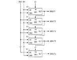
- FIG. 61 is a block diagram showing a configuration of the shift register described in Patent Document 1.
- the shift register shown in FIG. 61 is configured by connecting the unit circuits 91 shown in FIG. 62 in multiple stages, and operates according to the timing chart shown in FIG.
- This shift register employs a bootstrap system.
- the threshold voltage of the transistor is Vth and the high level potential is VDD.
- the unit circuit 91 is supplied with the output signal OUT (or the start pulse ST) of the previous unit circuit 91 as the input signal IN.
- the transistor Q2 When the input signal IN goes high, the transistor Q2 is turned on and the potential of the node N1 rises to (VDD ⁇ Vth).
- the clock signal CK changes from the low level to the high level, the potential of the node N1 is pushed up to (VDD ⁇ Vth + ⁇ ) by the gate-channel capacitance of the transistor Q1 and the capacitance C1, where ⁇ is Approximately equal to the amplitude of the clock signal CK).
- VDD ⁇ Vth + ⁇ > VDD + Vth is established, so that when the clock signal CK passes through the transistor Q1, the high level potential of the clock signal CK does not decrease by the threshold voltage of the transistor Q1. Therefore, the high level potential VDD without a threshold drop can be output as the output signal OUT.
- the conventional shift register has the following problems when the threshold voltage of the transistor is high.
- the threshold voltage of a transistor may be originally high due to manufacturing variations, or may be high due to a temperature change or transistor deterioration.
- the threshold voltage Vth is high, the on-state current of the transistor Q2 decreases, so that the potential of the node N1 may not reach (VDD ⁇ Vth) within the high level period of the input signal IN.
- the potential of the node N1 is (VDD ⁇ Vth ⁇ ) (where ⁇ > 0) when the input signal IN changes to the low level, the gate ⁇ of the transistor Q1 is output during the high level period of the output signal OUT.
- an object of the present invention is to provide a shift register having a large operation margin with respect to fluctuations in the threshold voltage of a transistor.
- a first aspect of the present invention is a shift register having a configuration in which a plurality of unit circuits are connected in multiple stages,
- the unit circuit is An output transistor having a first conduction terminal connected to a clock terminal for inputting a clock signal and a second conduction terminal connected to an output terminal for outputting the clock signal;
- An on-potential output unit that outputs an on-potential applied to the control terminal of the output transistor;
- a set control unit for switching on and off potentials to be applied to the control terminal of the set transistor;
- the set control unit controls the control terminal of the set transistor to be in a floating state during a part of a period in which an ON potential is applied to the control terminal of the output transistor.
- a second aspect of the present invention is a shift register having a configuration in which a plurality of unit circuits are connected in multiple stages,
- the unit circuit is An output transistor having a first conduction terminal connected to a clock terminal for inputting a clock signal and a second conduction terminal connected to an output terminal for outputting the clock signal;
- a withstand voltage transistor having a first conduction terminal connected to the first node, a second conduction terminal connected to a control terminal of the output transistor, and an ON potential fixedly applied to the control terminal;
- An on-potential output unit that outputs an on-potential applied to the first node;
- a set control unit for switching on and off potentials to be applied to the control terminal of the set transistor;
- the set control unit controls the control terminal of the set transistor to be in a floating state during a part of a period in which an ON potential
- the on-potential output unit outputs an input signal to the unit circuit
- the set control unit includes a transistor in which a second clock signal is supplied to a first conduction terminal, a second conduction terminal is connected to a control terminal of the set transistor, and an ON potential is fixedly applied to the control terminal. It is characterized by.
- the on-potential output unit outputs an input signal to the unit circuit
- the set control unit includes a transistor in which the input signal is given to a first conduction terminal, a second conduction terminal is connected to a control terminal of the set transistor, and an ON potential is fixedly applied to the control terminal.
- the on-potential output unit outputs an on-potential fixedly
- the set control unit includes a transistor in which an input signal to the unit circuit is given to a first conduction terminal, a second conduction terminal is connected to a control terminal of the set transistor, and an ON potential is fixedly applied to the control terminal. It is characterized by including.
- the on-potential output unit outputs a first input signal to the unit circuit
- the set control unit includes a transistor in which a second input signal to the unit circuit is supplied to a first conduction terminal and a control terminal, and the second conduction terminal is connected to a control terminal of the set transistor.
- the on-potential output unit outputs a first input signal to the unit circuit
- the set control unit is a transistor in which a second clock signal is given to a first conduction terminal, a second conduction terminal is connected to a control terminal of the set transistor, and a second input signal to the unit circuit is given to the control terminal. It is characterized by including.
- the on-potential output unit outputs a first input signal to the unit circuit
- the set control unit is a transistor in which a second input signal to the unit circuit is given to a first conduction terminal, a second conduction terminal is connected to a control terminal of the set transistor, and a second clock signal is given to the control terminal It is characterized by including.
- the on-potential output unit outputs a first input signal to the unit circuit
- a second input signal to the unit circuit is supplied to a first conduction terminal, the second conduction terminal is connected to a control terminal of the set transistor, and an ON potential is fixedly applied to the control terminal.
- a transistor is included.
- the on-potential output unit outputs an input signal to the unit circuit
- the set control unit includes a transistor in which a second clock signal is supplied to a first conduction terminal and a control terminal, and the second conduction terminal is connected to a control terminal of the set transistor.
- An eleventh aspect of the present invention is a display device, A plurality of scan lines arranged parallel to each other; A plurality of data lines arranged in parallel to each other so as to be orthogonal to the scanning lines; A plurality of pixel circuits arranged corresponding to the intersections of the scanning lines and the data lines; As a scanning line driving circuit for driving the scanning line, a shift register according to the first or second invention is provided.
- a twelfth aspect of the present invention is a shift register control method having a configuration in which a plurality of unit circuits are connected in multiple stages, An output transistor having a first conduction terminal connected to a clock terminal for inputting a clock signal and a second conduction terminal connected to an output terminal for outputting the clock signal; and a second conduction terminal.
- the step of controlling the potential of the control terminal of the set transistor is characterized in that the control terminal of the set transistor is controlled to be in a floating state during a part of a period in which an ON potential is applied to the control terminal of the output transistor.
- a thirteenth aspect of the present invention is a shift register control method having a configuration in which a plurality of unit circuits are connected in multiple stages, An output transistor having a first conduction terminal connected to a clock terminal for inputting a clock signal and a second conduction terminal connected to an output terminal for outputting the clock signal; and a first conduction terminal. Is connected to the first node, the second conduction terminal is connected to the control terminal of the output transistor, the withstand voltage transistor having a fixed ON potential applied to the control terminal, and the second conduction terminal to the first node.
- Including connected set transistors Outputting an on potential applied to the first node to the first conduction terminal of the set transistor;
- a step of switching and applying an on potential and an off potential to the control terminal of the set transistor The step of controlling the potential of the control terminal of the set transistor is characterized in that the control terminal of the set transistor is controlled to be in a floating state during a part of a period in which an ON potential is applied to the first node.
- the potential of the control terminal of the set transistor is set to a sufficient on potential (in the case where the on potential is a high level potential).
- the potential of the control terminal of the output transistor is an on-potential that does not drop the threshold value because the potential is higher than the normal on-potential. . Therefore, when outputting a clock signal having an on potential, the potential of the control terminal of the output transistor can be changed to a sufficient on potential to reduce the rounding of the output signal.
- the influence of waveform rounding can be suppressed and the operation margin with respect to the fluctuation of the threshold voltage of the transistor can be increased.
- the potential of the control terminal of the set transistor since the potential of the control terminal of the set transistor becomes a sufficient on potential after the control terminal of the set transistor enters the floating state, the potential of the first node is the threshold value. It becomes the on potential without dropping. Therefore, when outputting a clock signal having an on potential, the same effect as that of the first aspect can be obtained by changing the potential of the control terminal of the output transistor to a sufficient on potential. Further, the potential of the first node does not change from the on-potential output from the on-potential output unit when the clock signal having the on-potential is output due to the action of the withstand voltage transistor. Therefore, it is possible to prevent a voltage higher than the driving voltage of the transistor from being applied between the terminals of the transistor connected to the first node.
- the control terminal of the set transistor floats after the potential of the control terminal of the set transistor reaches a predetermined level. It becomes a state. Thereafter, when the potential of the control terminal of the output transistor (or the potential of the first node) continues to change toward the on potential, the potential of the control terminal of the set transistor becomes a sufficient on potential, and the control terminal of the output transistor The potential (or the potential of the first node) is an on potential without a threshold drop. Therefore, the same effect as the first aspect (or the second aspect) can be obtained.
- the control terminal of the set transistor when the potential of the input signal changes to the on-potential, the control terminal of the set transistor enters a floating state after the potential of the control terminal of the set transistor reaches a predetermined level. Become. Thereafter, when the potential of the control terminal of the output transistor (or the potential of the first node) continues to change toward the on potential, the potential of the control terminal of the set transistor becomes a sufficient on potential, and the control terminal of the output transistor The potential (or the potential of the first node) is an on potential without a threshold drop. Therefore, the same effect as the first aspect (or the second aspect) can be obtained.
- the control terminal of the set transistor floats after the potential of the control terminal of the set transistor reaches a predetermined level. It becomes a state.
- the potential of the control terminal of the set transistor becomes a sufficient ON potential.
- the potential of the control terminal of the output transistor becomes an on potential without dropping the threshold. Therefore, the same effect as the first aspect (or the second aspect) can be obtained.
- the potential of the control terminal of the set transistor is changed to the on potential based on the second input signal
- the potential of the control terminal of the output transistor is changed to the on potential based on the first input signal.
- the set transistor when the potentials of the second input signal and the second clock signal change to the on potential, the set transistor after the potential of the control terminal of the set transistor reaches a predetermined level.
- the control terminal is in a floating state.
- the operation margin can be increased.
- the control terminal of the set transistor when the potential of the second clock signal changes to the on potential, the control terminal of the set transistor enters a floating state after the potential of the control terminal of the set transistor reaches a predetermined level. . After that, when the potential of the input signal changes to the on potential and the potential of the control terminal of the output transistor (or the potential of the first node) changes to the on potential, the potential of the control terminal of the set transistor becomes a sufficient on potential.
- the potential of the control terminal of the output transistor (or the potential of the first node) is an on potential without dropping the threshold. Therefore, the same effect as the first aspect (or the second aspect) can be obtained.
- the potential of the control terminal of the set transistor is changed to the on potential based on the second clock signal
- the potential of the control terminal of the output transistor is changed to the on potential based on the input signal.
- the operation margin can be increased.
- the shift register according to the first or second aspect as a scanning line driving circuit, the rounding of the output signal of the scanning line driving circuit is reduced, and the threshold voltage of the transistor It is possible to increase the operation margin with respect to fluctuations.
- FIG. 3 is a circuit diagram of a unit circuit of the shift register according to the first embodiment.
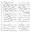
- FIG. 3 is a timing chart of the shift register according to the first embodiment. It is a signal waveform diagram of the shift register according to the first embodiment.
- FIG. 5 is a circuit diagram of a unit circuit of a shift register according to a second embodiment.
- FIG. 6 is a circuit diagram of a unit circuit of a shift register according to a third embodiment. It is a signal waveform diagram of the shift register according to the third embodiment.
- FIG. 9 is a circuit diagram of a unit circuit of a shift register according to a fourth embodiment. It is a block diagram which shows the structure of the shift register which concerns on 5th Embodiment.
- FIG. 10 is a circuit diagram of a unit circuit of a shift register according to a fifth embodiment.
- FIG. 10 is a circuit diagram of a unit circuit of a shift register according to a sixth embodiment. It is a signal waveform diagram of the shift register according to the sixth embodiment. It is a block diagram which shows the structure of the shift register which concerns on 7th Embodiment.
- FIG. 10 is a circuit diagram of a unit circuit of a shift register according to a seventh embodiment.
- FIG. 10 is a timing chart at the time of backward scanning of the shift register according to the seventh embodiment.
- FIG. 20 is a circuit diagram of a unit circuit of a shift register according to an eighth embodiment. It is a signal waveform diagram of the shift register according to the eighth embodiment.
- FIG. 10 is a circuit diagram of a unit circuit of a shift register according to a ninth embodiment.
- FIG. 20 is a circuit diagram of a unit circuit of a shift register according to a tenth embodiment.
- FIG. 20 is a circuit diagram of a unit circuit of a shift register according to a twelfth embodiment. It is a circuit diagram of the unit circuit of the shift register which concerns on 13th Embodiment. It is a circuit diagram of the unit circuit of the shift register which concerns on 14th Embodiment.
- FIG. 20 is a circuit diagram of a unit circuit of a shift register according to a fifteenth embodiment.
- FIG. 29 is a circuit diagram of a unit circuit of a shift register according to a sixteenth embodiment.
- FIG. 23 is a circuit diagram of a unit circuit of a shift register according to a seventeenth embodiment. It is a signal waveform diagram of the shift register according to the seventeenth embodiment.
- FIG. 29 is a circuit diagram of a unit circuit of a shift register according to an eighteenth embodiment.
- FIG. 29 is a circuit diagram of a unit circuit of a shift register according to a nineteenth embodiment.
- FIG. 20 is a circuit diagram of a unit circuit of a shift register according to a fifteenth embodiment.
- FIG. 29 is a circuit diagram of a unit circuit of a shift register according to a sixteenth embodiment.
- FIG. 23 is a circuit diagram of a unit circuit of a shift register according to a seventeenth embodiment. It is a signal waveform diagram of the shift register according
- FIG. 34 is a circuit diagram of a unit circuit of a shift register according to a twentieth embodiment.
- FIG. 38 is a circuit diagram of a unit circuit of a shift register according to the twenty-first embodiment.
- FIG. 23 is a signal waveform diagram of the shift register according to the twenty-first embodiment. It is a block diagram which shows the structure of the shift register which concerns on 22nd Embodiment.
- FIG. 34 is a circuit diagram of a unit circuit of a shift register according to a twenty-second embodiment. It is a signal waveform diagram of the shift register according to the twenty-second embodiment.
- FIG. 38 is a circuit diagram of a unit circuit of a shift register according to a twenty-third embodiment.
- FIG. 38 is a signal waveform diagram of the shift register according to the twenty-third embodiment.
- FIG. 24 is a timing chart of the shift register according to the twenty-fourth embodiment. It is a block diagram which shows the structure of the shift register which concerns on 25th Embodiment.
- FIG. 29 is a circuit diagram of a unit circuit of a shift register according to a twenty-fifth embodiment. It is a signal waveform diagram of the shift register according to the twenty-fifth embodiment. It is a block diagram which shows the structure of the shift register which concerns on the modification of 25th Embodiment.
- FIG. 53 is a timing chart of the shift register shown in FIG. 52.
- FIG. 38 is a circuit diagram of a unit circuit of a shift register according to a twenty-sixth embodiment. It is a block diagram which shows the 1st structural example of the liquid crystal display device provided with the shift register which concerns on embodiment of this invention. It is a block diagram which shows the 2nd structural example of the liquid crystal display device provided with the shift register which concerns on embodiment of this invention. It is a block diagram which shows the 3rd structural example of the liquid crystal display device provided with the shift register which concerns on embodiment of this invention.
- FIG. 58 is a timing chart of the liquid crystal display device shown in FIG. 57.
- FIG. It is a block diagram which shows the 4th structural example of the liquid crystal display device provided with the shift register which concerns on embodiment of this invention.
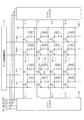
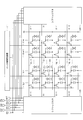
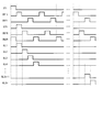
- FIG. 60 is a timing chart of the liquid crystal display device shown in Fig. 59. It is a block diagram which shows the structure of the conventional shift register. It is a circuit diagram of the unit circuit of the conventional shift register. It is a timing chart of the conventional shift register.
- a shift register when a conduction terminal of a transistor becomes both a source terminal and a drain terminal, one conduction terminal is fixedly called a source terminal, and the other conduction terminal is fixedly called a drain terminal. Further, a signal input or output through a certain terminal is called with the same name as the terminal (for example, a signal input through the clock terminal CKA is called a clock signal CKA).
- a potential at which the transistor is turned on when supplied to the gate terminal is referred to as an on potential, and a potential at which the transistor is turned off is referred to as an off potential.
- an on potential For example, for an N-channel transistor, a high level potential is an on potential and a low level potential is an off potential.
- the threshold voltage of the transistor is Vth, the high level potential is VDD, and the low level potential is VSS.
- each transistor shown below may be composed of two or more transistors connected in series.
- each transistor described below may be constituted by a TFT.
- a channel layer is formed using InGaZnOx (also referred to as “IGZO”) which is an oxide semiconductor containing indium (In), gallium (Ga), zinc (Zn), and oxygen (O) as main components.
- IGZO-TFT may be used.
- FIG. 1 is a diagram showing a basic configuration of a unit circuit included in a shift register according to an embodiment of the present invention.
- a unit circuit 1 shown in FIG. 1 includes transistors Tr1 and Tr2, an on-potential output unit 2, and a set control unit 3.
- the drain terminal of the transistor Tr1 is connected to the clock terminal CKA, and the source terminal of the transistor Tr1 is connected to the output terminal OUT.
- the output of the on-potential output unit 2 is given to the drain terminal of the transistor Tr2, the source terminal of the transistor Tr2 is connected to the gate terminal of the transistor Tr1, and the output of the set control unit 3 is given to the gate terminal of the transistor Tr2.
- the transistor Tr1 functions as an output transistor
- the transistor Tr2 functions as a set transistor.
- the on-potential output unit 2 outputs an on-potential applied to the gate terminal of the transistor Tr1.
- the set control unit 3 applies the switching between the on potential and the off potential to the gate terminal of the transistor Tr2.
- the set control unit 3 controls the gate terminal of the transistor Tr2 to be in a floating state during a part of the period in which the ON potential is applied to the gate terminal of the transistor Tr1.
- the transistors Tr1 and Tr2 are N-channel type, but the transistors Tr1 and Tr2 may be P-channel type.
- FIG. 2 is a block diagram showing the configuration of the shift register according to the first embodiment of the present invention.
- the shift register 10 shown in FIG. 2 is configured by connecting n (n is an integer of 2 or more) unit circuits 11 in multiple stages.
- the unit circuit 11 has clock terminals CKA and CKB, an input terminal IN, and an output terminal OUT.
- a start pulse ST and two-phase clock signals CK1 and CK2 are supplied to the shift register 10 from the outside.
- the start pulse ST is given to the input terminal IN of the unit circuit 11 in the first stage.
- the clock signal CK1 is supplied to the clock terminal CKA of the odd-numbered unit circuit 11 and the clock terminal CKB of the even-numbered unit circuit 11.
- the clock signal CK2 is supplied to the clock terminal CKA of the even-numbered unit circuit 11 and the clock terminal CKB of the odd-numbered unit circuit 11.
- the output signal OUT of the unit circuit 11 is output to the outside as output signals O1 to On, and is given to the input terminal IN of the unit circuit 11 at the next stage.
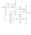
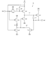
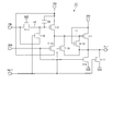
- FIG. 3 is a circuit diagram of the unit circuit 11.
- the unit circuit 11 shown in FIG. 3 includes three N-channel transistors Tr1 to Tr3.
- the drain terminal of the transistor Tr1 is connected to the clock terminal CKA, and the source terminal of the transistor Tr1 is connected to the output terminal OUT.
- the drain terminal of the transistor Tr2 is connected to the input terminal IN, and the source terminal of the transistor Tr2 is connected to the gate terminal of the transistor Tr1.
- the drain terminal of the transistor Tr3 is connected to the clock terminal CKB, the source terminal of the transistor Tr3 is connected to the gate terminal of the transistor Tr2, and the high level potential VDD is applied to the gate terminal of the transistor Tr3.
- the transistors Tr1 to Tr3 function as an output transistor, a set transistor, and a set control unit, respectively, and the input terminal IN functions as an ON potential output unit.
- n1 the node to which the gate terminal of the transistor Tr1 is connected
- n2 the node to which the gate terminal of the transistor Tr2 is connected
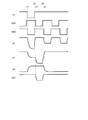
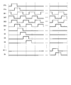
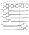
- FIG. 4 is a timing chart of the shift register 10. As shown in FIG. 4, the clock signal CK1 becomes a high level and a low level at a predetermined cycle. However, the high level period of the clock signal CK1 is shorter than the low level period of the clock signal CK1.
- the clock signal CK2 is a signal obtained by delaying the clock signal CK1 by a half cycle.
- the start pulse ST becomes high level during the high level period of the clock signal CK2 at the start of shifting.
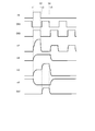
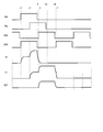
- FIG. 5 is a signal waveform diagram of the shift register 10. The operation of the unit circuit 11 will be described with reference to FIG.
- the potentials of the nodes n1 and n2 and the output signal OUT are at a low level.
- the input signal IN and the clock signal CKB change from the low level to the high level. Accordingly, a current passing through the transistor Tr3 flows from the clock terminal CKB toward the node n2, and the potential of the node n2 rises (charge of the node n2).
- the transistor Tr2 is turned on.
- the transistor Tr3 When the potential of the node n2 rises to (VDD ⁇ Vth), the transistor Tr3 is turned off, and the node n2 is in a floating state thereafter. Even after the transistor Tr3 is turned off, the potential of the node n1 continues to rise. When the potential of the node n1 rises, the potential of the node n2 is pushed up and raised by the gate-source capacitance and the gate-channel capacitance of the transistor Tr2 (pushing up the node n2). When the potential of the node n2 becomes (VDD + Vth) or more, the potential of the node n1 becomes the high level potential VDD.
- the clock signal CKB and the input signal IN change to a low level.
- the transistor Tr3 is turned on, and a current passing through the transistor Tr3 flows from the node n2 toward the clock terminal CKB, and the potential of the node n2 drops to a low level (discharge of the node n2).
- the transistor Tr2 is turned off. Even after the transistor Tr2 is turned off, the potential of the node n1 is kept at the high level potential VDD, and the transistor Tr1 is kept on.
- the clock signal CKA changes from the low level to the high level. Accordingly, after time t3, the high level potential of the clock signal CKA is output as the output signal OUT.
- the potential of the output signal OUT rises, the potential at the node n1 is pushed up by the gate-channel capacitance of the transistor Tr1 and rises by ⁇ (where ⁇ is approximately equal to the amplitude of the clock signal CKA) (node). n1 thrust).
- ⁇ is obtained by multiplying the amplitude of the clock signal CKA by (capacitance value of the capacitance between the gate and channel of the transistor Tr1) / (total of capacitance values of all the capacities associated with the node n1).
- the potential of the node n1 is equal to or higher than (VDD + Vth)
- the clock signal CKA passes through the transistor Tr1
- the high level potential of the clock signal CKA does not decrease by the threshold voltage of the transistor Tr1. Therefore, the high level potential VDD without a threshold drop can be output as the output signal OUT.
- the clock signal CKA changes to a low level.
- the output signal OUT changes to a low level. Further, since the pushing up of the node n1 is finished, the potential of the node n1 falls to the high level potential VDD.
- the clock signal CKB changes to high level. Accordingly, the potential of the node n2 rises to (VDD ⁇ Vth), and the transistor Tr2 is turned on. At this time, since the input signal IN is at a low level, a current passing through the transistor Tr2 flows from the node n1 toward the input terminal IN, and the potential of the node n1 decreases to become a low level (discharge of the node n1). As described above, the output signal OUT of the unit circuit 11 becomes high level during the high level period of the clock signal CKA after the input signal IN becomes high level. At this time, the potential of the output signal OUT becomes the high level potential VDD with no threshold drop.
- the output signal O1 of the first stage unit circuit 11 becomes high level during the high level period of the clock signal CK1 after the start pulse ST becomes high level.
- the output signal O2 of the second stage unit circuit 11 becomes high level during the high level period of the clock signal CK2 after the output signal O1 becomes high level.
- the output signal Oi of the unit circuit 11 becomes high level in the high level period of the clock signal CK1 or CK2 after the output signal Oi-1 of the unit circuit 11 in the previous stage becomes high level. Therefore, the output signals O1 to On of the shift register 10 become high level in ascending order (in the order of O1, O2,..., On) with a delay of half a cycle of the clock signal CK1.
- the unit circuit 11 includes the output transistor Tr1 having the first conduction terminal connected to the clock terminal CKA and the second conduction terminal connected to the output terminal OUT, and the ON potential (high) applied to the control terminal of the output transistor Tr1.
- On-potential output section (input terminal IN) that outputs (level potential), and the output of the on-potential output section is applied to the first conduction terminal, and the second conduction terminal is set transistor Tr2 connected to the control terminal of the output transistor Tr1
- a set control unit for switching on and applying an ON potential and an OFF potential (low level potential) to the control terminal of the set transistor Tr2.
- the on-potential output unit outputs an input signal IN to the unit circuit 11, the set control unit is supplied with the second clock signal CKB to the first conduction terminal, and the second conduction terminal is connected to the control terminal of the set transistor Tr2. And a transistor Tr3 in which the ON potential is fixedly applied to the control terminal.
- the control terminal of the set transistor Tr2 enters a floating state after the potential of the control terminal of the set transistor Tr2 reaches a predetermined level (VDD-Vth). Become. Thereafter, when the potential of the control terminal of the output transistor Tr1 continues to change toward the ON potential (continues to rise), the potential of the control terminal of the set transistor Tr2 becomes a sufficient ON potential (potential higher than a normal high level potential). Thus, the potential of the control terminal of the output transistor Tr1 becomes the on potential VDD without a threshold drop.
- the shift register 10 when outputting a clock signal having an on potential, the potential of the output transistor Tr1 is changed to a sufficient on potential to reduce the rounding of the output signal OUT. Can do. Further, even when the threshold voltage of the transistor is originally high or becomes high due to a temperature change or deterioration of the transistor, the influence of waveform rounding can be suppressed and the operation margin with respect to the fluctuation of the threshold voltage of the transistor can be increased.
- the shift register according to the second embodiment of the present invention has the configuration shown in FIG.
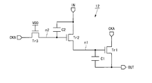
- the shift register according to the present embodiment includes a unit circuit 12 shown in FIG.
- the unit circuit 12 is obtained by adding capacitors C1 and C2 to the unit circuit 11 (FIG. 3).
- the capacitor C1 is provided between the gate and the source of the transistor Tr1, and the capacitor C2 is provided between the gate and the drain of the transistor Tr2. Only one of the capacitors C1 and C2 may be provided.
- the effect of pushing up the node n1 when the output signal OUT changes from the low level to the high level can be increased.
- the capacitor C2 By providing the capacitor C2, the effect of pushing up the node n2 when the input signal IN changes from the low level to the high level can be increased.
- the shift register of this embodiment by increasing the push-up effect of the nodes n1 and n2, the high-level potential VDD without a threshold drop is more reliably output as the output signal OUT, and the variation in the threshold voltage of the transistor is prevented.
- the operating margin can be further increased.
- the shift register according to the third embodiment of the present invention has the configuration shown in FIG.
- the shift register according to the present embodiment includes a unit circuit 13 shown in FIG.
- the unit circuit 13 is obtained by adding N-channel transistors Tr4 to Tr7 and a resistor R1 to the unit circuit 12 (FIG. 6).
- the drain terminal of the transistor Tr4 is connected to the gate terminal of the transistor Tr1.
- a high level potential VDD is applied to the drain terminal of the transistor Tr5, and the source terminal of the transistor Tr5 is connected to one end of the resistor R1.
- the other end of the resistor R1 is connected to the gate terminal of the transistor Tr4 and the drain terminals of the transistors Tr6 and Tr7.
- a low level potential VSS is applied to the source terminals of the transistors Tr4, Tr6, Tr7.
- the gate terminals of the transistors Tr5 to Tr7 are connected to the clock terminal CKB, the input terminal IN, and the output terminal OUT, respectively.
- the node to which the gate terminal of the transistor Tr4 is connected is referred to as n3.
- FIG. 8 is a signal waveform diagram of the shift register according to the present embodiment.
- the signal waveform diagram shown in FIG. 8 is obtained by adding a change in the potential of the node n3 to the signal waveform diagram shown in FIG. Prior to time t1, the potential of the node n3 is (VDD ⁇ Vth).
- the transistors Tr5 and Tr6 are turned on.
- the current limit by the resistor R1 causes the potential of the node n3 to fall to a low level potential close to VSS, so that the transistor Tr4 is turned off.
- the clock signal CKB and the input signal IN change to low level at time t2
- the transistors Tr5 and Tr6 are turned off.
- the potential of the node n3 is kept at a low level.
- the clock signal CKB changes to high level at time t5
- the transistor Tr5 is turned on and the potential of the node n3 rises to (VDD ⁇ Vth), so that the transistor Tr4 is turned on.
- the transistor Tr2 is turned on. Therefore, the potential of the node n1 is rapidly changed to a low level by the action of the transistors Tr2 and Tr4.
- the clock signal CKB periodically becomes a high level, and the transistor Tr5 is periodically turned on. For this reason, even if the potential of the node n3 drops due to the off-leakage current of the transistors Tr6 and Tr7, the potential of the node n3 periodically becomes (VDD ⁇ Vth). Therefore, according to the shift register of this embodiment, the potential of the node n3 can be kept at a high level during the off period of the transistor Tr1.
- the potential of the node n2 periodically becomes a low level, and the transistor Tr2 is periodically turned off. Therefore, if the transistor Tr4 is not provided, noise may be generated in the potential of the node n1 when the clock signal CKA becomes high level when the transistor Tr2 is in an off state, and the transistor Tr1 may be erroneously turned on.
- the potential of the node n1 is fixed at a low level during the off-period of the transistor Tr1. Therefore, according to the shift register according to the present embodiment, it is possible to prevent malfunction caused by the change of the clock signal CKA.
- the potential of the node n3 may increase due to the off-leakage current of the transistor Tr5 during the high level period of the output signal OUT, the transistor Tr4 may be turned on, and the potential of the node n1 may decrease.
- the potential of the node n3 is fixed to a low level during the high level period of the output signal OUT using the transistor Tr7. Therefore, according to the shift register according to the present embodiment, it is possible to prevent a malfunction caused by an increase in the potential of the node n3.
- a unit circuit in which the transistor Tr5 and the resistor R1 are connected in reverse order (a high level potential VDD is applied to one end of the resistor R1, and the other end of the resistor R1 is connected to the drain terminal of the transistor Tr5).
- a circuit in which the source terminal of the transistor Tr5 is connected to the gate terminal of the transistor Tr4 and the drain terminals of the transistors Tr6 and Tr7 may be used. According to the shift register including the unit circuit, the same effect as that of the shift register including the unit circuit 13 can be obtained.
- the shift register according to the fourth embodiment of the present invention has the configuration shown in FIG.
- the shift register according to the present embodiment includes a unit circuit 14 shown in FIG. 9 instead of the unit circuit 11.
- the unit circuit 14 is obtained by adding an N-channel transistor Tr8 to the unit circuit 13 (FIG. 7).
- the drain terminal of the transistor Tr8 is connected to the output terminal OUT, the low level potential VSS is applied to the source terminal of the transistor Tr8, and the gate terminal of the transistor Tr8 is connected to the node n3.
- the output signal OUT changes from high level to low level, it is necessary to keep the low level until the input signal IN next becomes high level.
- the output signal OUT cannot be kept at a low level due to an off-leakage current of the transistor Tr1 or a leakage current in a circuit connected to the output terminal OUT, and the shift register may malfunction.
- the transistor Tr8 is used, and the output signal OUT is fixed at a low level during the off period of the transistor Tr1. Therefore, according to the shift register according to the present embodiment, it is possible to prevent malfunction caused by the potential increase of the output signal OUT.
- FIG. 10 is a block diagram showing a configuration of a shift register according to the fifth embodiment of the present invention.
- the shift register 20 shown in FIG. 10 is configured by connecting n unit circuits 21 in multiple stages.
- the unit circuit 21 has clock terminals CKA and CKB, an input terminal IN, an initialization terminal INIT, and an output terminal OUT.
- a start pulse ST, two-phase clock signals CK1 and CK2, and an initialization signal INIT are supplied to the shift register 20 from the outside.
- the initialization signal INIT is supplied to the initialization terminals INIT of the n unit circuits 21.
- Other signals are applied to the respective terminals in the same manner as the shift register (FIG. 2) according to the first embodiment.
- FIG. 11 is a circuit diagram of the unit circuit 21.
- the unit circuit 21 is obtained by adding an N-channel transistor Tr9 to the unit circuit 14 (FIG. 9).
- the gate terminal and the drain terminal of the transistor Tr9 are connected to the initialization terminal INIT, and the source terminal of the transistor Tr9 is connected to the node n3.
- the initialization signal INIT is controlled to a high level immediately after the power is turned on, when the power is turned off, when the shift register is temporarily set to the initial state, etc., and is controlled to a low level otherwise.
- the transistor Tr9 is turned off, and the unit circuit 21 operates in the same manner as the unit circuit 14.
- the transistor Tr9 is turned on, and the potential of the node n3 rises to (VDD ⁇ Vth). For this reason, the transistor Tr8 is turned on, and the output signal OUT becomes a low level.
- the transistor Tr4 since the transistor Tr4 is also turned on, the potential of the node n1 becomes a low level, and the transistor Tr1 is turned off. Therefore, the output signal OUT is surely at a low level.
- the potential of the node n1 and the output signal OUT can be initialized to a low level and the potential of the node n3 can be initialized to a high level using the transistor Tr9.
- the unit circuit 21 may include a transistor in which the gate terminal is connected to the initialization terminal INIT and the high level potential VDD is applied to the drain terminal, instead of the transistor Tr9. Even if this transistor is used, the same initialization can be performed.
- the shift register according to the sixth embodiment of the present invention has the configuration shown in FIG.
- the shift register according to the present embodiment includes a unit circuit 22 shown in FIG.
- the unit circuit 22 is obtained by adding an N-channel transistor Tr10 to the unit circuit 21 (FIG. 11).
- the drain terminal of the transistor Tr10 is connected to the source terminal of the transistor Tr2, the source terminal of the transistor Tr10 is connected to the gate terminal of the transistor Tr1, and the high level potential VDD is applied to the gate terminal of the transistor Tr10.
- the transistor Tr10 functions as a withstand voltage transistor.
- n4 the node to which the drain terminal of the transistor Tr10 is connected
- n5 the node to which the source terminal of the transistor Tr10 is connected
- the potential of the node n1 becomes the maximum (VDD ⁇ Vth + ⁇ ) by pushing up.
- a high voltage of (VDD ⁇ Vth + ⁇ VSS) is applied between the gate and source and between the source and drain of the transistor Tr2.
- the same high voltage is also applied between the gate and drain of the transistor Tr4 and between the source and drain.
- the unit circuit 22 includes a transistor Tr10.
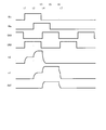
- FIG. 13 is a signal waveform diagram of the shift register according to the present embodiment.
- the signal waveform diagram shown in FIG. 13 is obtained by deleting the potential change at the node n1 from the signal waveform diagram shown in FIG. 8 and adding the potential change at the nodes n4 and n5.
- the potential of the node n4 rises to the high level potential VDD that does not drop the threshold.
- the transistor Tr10 since the transistor Tr10 is in an on state, when the potential of the node n4 changes from the low level to the high level, the potential of the node n5 also changes in the same manner (charging of the node n5).
- the potential of the node n5 becomes the maximum (VDD ⁇ Vth + ⁇ ) by pushing up.
- a voltage (VDD-VSS) lower than the drive voltage of the transistor is applied between the gate and source and between the source and drain of the transistor Tr2.
- the same voltage is also applied between the gate and drain and between the source and drain of the transistor Tr4.
- a voltage ( ⁇ Vth) is applied between the gate and source and between the source and drain of the transistor Tr10. Since ⁇ is only the amplitude of the clock signal CKA at the maximum, this voltage is also lower than the driving voltage of the transistor.
- the transistors Tr2 and Tr4 can be prevented from being deteriorated or destroyed.
- the operation margin can be increased while preventing deterioration and destruction of the transistor as compared with the case where the withstand voltage countermeasure is taken for the shift register not including the transistor Tr3.
- the unit circuit 22 includes the output transistor Tr1 having the first conduction terminal connected to the clock terminal CKA, the second conduction terminal connected to the output terminal OUT, and the first conduction terminal to the first node (node n4).
- a withstand voltage transistor Tr10 having a second conduction terminal connected to the control terminal of the output transistor Tr1, an on-potential (high level potential) fixedly applied to the control terminal, and an on-potential applied to the first node;
- It includes a set controller (transistor Tr3) that switches on and off the terminal to apply the on potential and the off potential.
- the on-potential output unit outputs an input signal IN to the unit circuit 22, and the set control unit is supplied with the second clock signal CKB to the first conduction terminal, and the second conduction terminal is connected to the control terminal of the set transistor Tr2. And a transistor Tr3 in which the ON potential is fixedly applied to the control terminal.
- the control terminal of the set transistor Tr2 enters a floating state after the potential of the control terminal of the set transistor Tr2 reaches a predetermined level (VDD-Vth). Become. Thereafter, when the potential of the first node continues to change toward the on potential (continues to rise), the potential of the control terminal of the set transistor Tr2 becomes a sufficient on potential (a potential higher than the normal high level potential) The potential of the first node becomes the on potential VDD with no threshold drop. Therefore, according to the shift register of this embodiment, it is possible to reduce the rounding of the output signal OUT and increase the operation margin with respect to the change in the threshold voltage of the transistor.
- the potential of the first node does not change from the on-potential output from the on-potential output section when the clock signal having the on-potential is output due to the action of the breakdown voltage transistor Tr10. Therefore, it is possible to prevent a high voltage from being applied between the terminals of the transistors Tr2 and Tr4 connected to the first node.
- FIG. 14 is a block diagram showing a configuration of a shift register according to the seventh embodiment of the present invention.
- the shift register 30 shown in FIG. 14 is configured by connecting n unit circuits 31 in multiple stages.
- the unit circuit 31 has clock terminals CKA and CKB, input terminals IN1 and IN2, an initialization terminal INIT, control terminals UD and UDB (not shown), and an output terminal OUT.
- a start pulse ST, two-phase clock signals CK1 and CK2, an initialization signal INIT, and control signals UD and UDB (not shown) are supplied to the shift register 30 from the outside.
- the clock signals CK1 and CK2 are given to each terminal similarly to the shift register 10 (FIG. 2) according to the first embodiment.
- the initialization signal INIT and the control signals UD and UDB are applied to the initialization terminal INIT and the control terminals UD and UDB of the n unit circuits 31, respectively.
- the start pulse ST is applied to the input terminal IN1 of the first stage unit circuit 31 and the input terminal IN2 of the nth stage unit circuit 31.
- the output signal OUT of the unit circuit 31 is output to the outside as output signals O1 to On, and is given to the input terminal IN1 of the next unit circuit 31 and the input terminal IN2 of the previous unit circuit 31.
- FIG. 15 is a circuit diagram of the unit circuit 31.
- the unit circuit 31 is obtained by adding a scan switching circuit 32 to the unit circuit 22 (FIG. 12).
- the scan switching circuit 32 functions as an on-potential output unit.
- the control signal UD is controlled to a high level during forward scanning, and is controlled to a low level during backward scanning.
- the control signal UDB is an inverted signal of the control signal UD.
- the scan switching circuit 32 outputs the input signal IN1 during forward scanning and the input signal IN2 during backward scanning.
- the output signal Os of the scan switching circuit 32 is given to the drain terminal of the transistor Tr2 and the gate terminal of the transistor Tr6.
- n6 the node to which the output terminal Os of the scan switching circuit 32 is connected.
- the unit circuit 31 operates using the output signal OUT of the previous unit circuit 31 as an input signal. At this time, the output signals O1 to On of the shift register 30 become high level in ascending order (see FIG. 4).
- the unit circuit 31 operates using the output signal OUT of the next unit circuit 31 as an input signal. At this time, the output signals O1 to On of the shift register 30 become high level in descending order (in order of On, On-1,..., O1) (see FIG. 16).
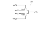
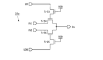
- FIG. 17 to 19 are circuit diagrams showing examples of the scan switching circuit 32.
- the scan switching circuit 32p since the high level potential output from the output terminal Os is (VDD ⁇ Vth), the operation margin is small. Therefore, in order to increase the operation margin, the scan switching circuit 32q shown in FIG. 18 or the scan switching circuit 32r shown in FIG. 19 may be used instead of the scan switching circuit 32p.
- the node to which the gate terminal of the transistor Tr34 is connected is referred to as n7.
- the potential of the node n7 becomes (VDD ⁇ Vth) by the action of the transistor Tr32, and the node n7 enters a floating state.
- the input signal IN1 changes from the low level to the high level
- the potential at the node n7 is pushed up and rises by the gate-channel capacitance of the transistor Tr34. Therefore, it is possible to output the high-level potential VDD without a threshold drop from the output terminal Os.
- the transistor Tr33 prevents a high voltage from being applied to the transistor Tr31 at this time.
- the transistors Tr31 and Tr33 are turned on, so that the potential of the node n7 is at a low level as with the control signal UD, and the transistor Tr34 is turned off.
- the scan switching circuit 32r it is possible to switch the scan direction while increasing the operation margin.
- the scan switching circuit 32q When the scan switching circuit 32q is used, (VDD ⁇ Vth) and VSS are applied to the gate terminals of the transistors Tr24 and Tr26, respectively, during forward scanning. During reverse scanning, VSS and (VDD ⁇ Vth) are applied to the gate terminals of the transistors Tr24 and Tr26, respectively. Therefore, the scan switching circuit 32q can provide the same effect as the scan switching circuit 32r.
- the operation margin with respect to the fluctuation of the threshold voltage of the transistor can be increased for the shift register that switches the scan direction. Further, by using the scan switching circuits 32q and 32r shown in FIG. 18 and FIG. 19, a high level potential VDD that does not drop the threshold is applied to the gate terminals of the transistors through which the input signals IN1 and IN2 pass, and the operation margin is increased. Can do.
- the shift register according to the eighth embodiment of the present invention has the configuration shown in FIG.
- the shift register according to the present embodiment includes a unit circuit 23 shown in FIG.
- the unit circuit 23 is obtained by changing the connection destination of the drain terminal of the transistor Tr3 to the input terminal IN in the unit circuit 22 (FIG. 12).
- FIG. 21 is a signal waveform diagram of the shift register according to the present embodiment.
- the signal waveform diagram shown in FIG. 21 is the same as the signal waveform diagram shown in FIG. 13 except that the potential of the node n2 remains low after time t5.
- the input signal IN changes to a high level at time t1
- a current passing through the transistor Tr3 flows from the input terminal IN toward the node n2, and the potential of the node n2 rises (charge of the node n2). Thereafter, charging of the node n5 and pushing up of the node n2 are performed.
- the input signal IN changes to a low level at time t2
- the potential of the node n2 falls and becomes a low level (discharge of the node n2).
- the potential of the node n2 is kept at a low level thereafter.
- the potential of the node n2 changes when the clock signal CKB changes.
- the potential of the node n2 changes when the input signal IN changes.
- the frequency with which the input signal IN changes is less than the frequency with which the clock signal CKB changes. Therefore, according to the shift register according to the present embodiment, charging / discharging of the parasitic capacitance associated with the node n2 can be reduced, and power consumption can be reduced.
- the on-potential output unit (input terminal IN) outputs the input signal IN to the unit circuit 22, and the set control unit receives the input signal IN to the first conduction terminal and the second conduction.
- the terminal includes a transistor Tr3 which is connected to the control terminal of the set transistor Tr2 and to which the ON potential (high level potential) is fixedly applied.
- the shift register according to the ninth embodiment of the present invention has the configuration shown in FIG.
- the shift register according to the present embodiment includes a unit circuit 24 shown in FIG.
- the unit circuit 24 is obtained by removing the capacitor C2 from the unit circuit 23 (FIG. 20) and applying the high level potential VDD to the drain terminal of the transistor Tr2.
- a terminal having the high-level potential VDD functions as an on-potential output unit.
- the signal waveform diagram of the shift register according to the present embodiment is the same as the signal waveform diagram shown in FIG.
- a current passing through the transistor Tr3 flows from the input terminal IN toward the node n2, and the potential of the node n2 rises (charge of the node n2).
- the transistor Tr2 is turned on. Since the high level potential VDD is applied to the drain terminal of the transistor Tr2, a current passing through the transistors Tr2 and Tr10 flows from the drain terminal of the transistor Tr2 toward the node n5, and the potential of the node n5 rises (at the node n5) charge).
- the node n2 is pushed up.
- the potential of the node n2 falls and becomes a low level (discharge of the node n2).
- the potential of the node n2 is kept at a low level thereafter. According to the shift register according to the present embodiment, as in the eighth embodiment, it is possible to reduce the charge / discharge of the parasitic capacitance associated with the node n2 and to reduce the power consumption.
- the on-potential output unit (terminal having the high-level potential VDD) outputs the on-potential (high-level potential) in a fixed manner
- the set control unit outputs the unit circuit 23 to the first conduction terminal.
- the second conduction terminal is connected to the control terminal of the set transistor Tr2, and the transistor Tr3 having the ON potential fixedly applied to the control terminal is included.
- the shift register according to the tenth embodiment of the present invention has the configuration shown in FIG.
- the shift register according to the present embodiment includes a unit circuit 15 shown in FIG.
- the unit circuit 15 is configured by forming the unit circuit 13 (FIG. 7) using a P-channel transistor.
- the unit circuit 15 includes seven P-channel transistors Trp1 to Trp7, capacitors C1 and C2, and a resistor R1.
- FIG. 24 is a signal waveform diagram of the shift register according to the present embodiment.
- the signal waveform diagram shown in FIG. 24 is obtained by inverting the polarities of the signal and the node potential with respect to the signal waveform diagram shown in FIG.
- an operation margin with respect to a change in the threshold voltage of the transistor can be increased in a shift register configured using a P-channel transistor.
- the unit circuit 13 according to the third embodiment is configured using P-channel transistors has been described, but the first, second, fourth to ninth embodiments, and The same method can be applied to unit circuits according to eleventh to twenty-sixth embodiments described later.
- FIG. 25 is a block diagram showing a configuration of a shift register according to the eleventh embodiment of the present invention.
- the shift register 40 shown in FIG. 25 is configured by connecting n unit circuits 41 in multiple stages.
- the unit circuit 41 has clock terminals CKA and CKB, input terminals INa and INb, and an output terminal OUT.
- the shift register 40 is supplied with start pulses STa and STb and four-phase clock signals CK1 to CK4 from the outside.
- the start pulse STa is applied to the input terminal INa of the first stage unit circuit 41 and the input terminal INb of the second stage unit circuit 41.
- the start pulse STb is given to the input terminal INb of the unit circuit 41 in the first stage.
- the output signal OUT of the unit circuit 41 is output to the outside as output signals O1 to On, and is given to the input terminal INa of the next stage unit circuit 41 and the input terminal INb of the unit circuit 41 of the second stage.
- the clock signal CK1 is the clock terminal CKA of the unit circuit 41 at the (4k-3) stage and the clock terminal CKB of the unit circuit 41 at the (4k-1) stage, where k is an integer between 1 and n / 4. Given to.
- the clock signal CK2 is supplied to the clock terminal CKA of the unit circuit 41 at the (4k-2) stage and the clock terminal CKB of the unit circuit 41 at the 4k stage.
- the clock signal CK3 is supplied to the clock terminal CKA of the unit circuit 41 at the (4k-1) stage and the clock terminal CKB of the unit circuit 41 at the (4k-3) stage.
- the clock signal CK4 is supplied to the clock terminal CKA of the unit circuit 41 at the 4k stage and the clock terminal CKB of the unit circuit 41 at the (4k-2) stage.
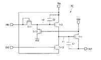
- FIG. 26 is a circuit diagram of the unit circuit 41.
- the unit circuit 41 shown in FIG. 26 includes five N-channel transistors Tr1, Tr2, Tr11 to Tr13.
- the drain terminal of the transistor Tr1 is connected to the clock terminal CKA, and the source terminal of the transistor Tr1 is connected to the output terminal OUT.
- the drain terminal of the transistor Tr2 is connected to the input terminal INa, and the source terminal of the transistor Tr2 is connected to the gate terminal of the transistor Tr1 and the drain terminal of the transistor Tr13.
- the gate terminal and drain terminal of the transistor Tr11 are connected to the input terminal INb, and the source terminal of the transistor Tr11 is connected to the gate terminal of the transistor Tr2 and the drain terminal of the transistor Tr12.
- the low level potential VSS is applied to the source terminal of the transistor Tr12, and the gate terminal of the transistor Tr12 is connected to the clock terminal CKA.
- the source terminal of the transistor Tr13 is connected to the input terminal INa, and the gate terminal of the transistor Tr13 is connected to the clock terminal CKB.
- the transistors Tr1 and Tr2 function as an output transistor and a set transistor, respectively, and the input terminal INa functions as an on-potential output unit.
- the transistors Tr11 and Tr12 function as a set control unit.
- FIG. 27 is a timing chart of the shift register 40.
- the clock signal CK1 becomes a high level and a low level at a predetermined cycle.
- the high level period of the clock signal CK1 is shorter than the low level period of the clock signal CK1.
- the clock signals CK2 to CK4 are signals obtained by delaying the clock signal CK1 by 1 ⁇ 4 period, half period, and 3 ⁇ 4 period, respectively.
- the start pulse STb becomes high level during the high level period of the clock signal CK3 at the start of shifting.
- the start pulse STa is a signal obtained by delaying the start pulse STb by a quarter cycle of the clock signal CK1.
- FIG. 28 is a signal waveform diagram of the shift register 40.
- the operation of the unit circuit 41 will be described with reference to FIG.
- the potentials of the nodes n1 and n2 and the output signal OUT are at a low level.
- the input signal INb and the clock signal CKB change from the low level to the high level.
- the transistor Tr11 is turned on, a current passing through the transistor Tr11 flows from the input terminal INb toward the node n2, and the potential of the node n2 rises (charging of the node n2).
- the transistor Tr11 is turned off, and the node n2 is in a floating state thereafter.
- the transistor Tr2 When the potential of the node n2 exceeds a predetermined level, the transistor Tr2 is turned on. At time t1, the transistor Tr13 is turned on. Thus, after a while from time t1, both the transistors Tr2 and Tr13 are turned on. At this time, since the input signal INa is at a low level, the potential of the node n1 is kept at a low level even after the transistors Tr2 and Tr13 are turned on.
- the input signal INa changes from the low level to the high level.
- the transistors Tr2 and Tr13 are in the on state, a current passing through the transistor Tr2 and a current passing through the transistor Tr13 flow from the input terminal INa toward the node n1, and the potential of the node n1 rises (charge of the node n1). ).
- the transistor Tr1 is turned on. Further, when the potential of the node n1 rises, the potential of the node n2 is pushed up and raised by the gate-channel capacitance of the transistor Tr2 (pushing up the node n2).
- the potential of the node n2 becomes (VDD + Vth) or more
- the potential of the node n1 becomes the high level potential VDD.
- the input signal INb and the clock signal CKB change to a low level. Accordingly, the transistor Tr13 is turned off. Even after the transistor Tr13 is turned off, the potentials of the nodes n1 and n2 are kept at a high level, and the transistor Tr1 is kept on.
- the clock signal CKA changes from the low level to the high level. Accordingly, after time t4, the high level potential of the clock signal CKA is output as the output signal OUT.
- the potential at the node n1 rises, the potential at the node n1 is pushed up by the gate-channel capacitance of the transistor Tr1 and rises by ⁇ (where ⁇ is approximately equal to the amplitude of the clock signal CKA) (node). n1 thrust).
- the potential of the node n1 is equal to or higher than (VDD + Vth), it is possible to output the high level potential VDD having no threshold drop as the output signal OUT.
- the transistor Tr12 is turned on at time t4, the potential of the node n2 becomes a low level (discharge of the node n2). For this reason, the transistor Tr2 is turned off. Thus, after a while from time t4, the transistors Tr2 and Tr13 are turned off, so that no current flows from the node n1 when the potential of the node n1 rises due to the push-up.
- the input signal INa changes to a low level.
- the transistors Tr2 and Tr13 are off, the potentials of the nodes n1 and n2 do not change.
- the clock signal CKA changes to a low level.
- the output signal OUT changes to a low level, and the transistor Tr12 is turned off.
- the clock signal CKB changes to a high level. Accordingly, the transistor Tr13 is turned on.
- the output signal O1 of the first stage unit circuit 41 becomes high level during the high level period of the clock signal CK1 after the start pulse STa becomes high level.
- the output signal O2 of the second stage unit circuit 41 becomes high level during the high level period of the clock signal CK2 after the output signal O1 becomes high level.
- the output signal O3 of the third stage unit circuit 41 becomes high level during the high level period of the clock signal CK3 after the output signal O2 becomes high level.
- the output signal O4 of the unit circuit 41 at the fourth stage becomes high level during the high level period of the clock signal CK4 after the output signal O3 becomes high level.
- the output signal Oi of the unit circuit 41 becomes high level during any high level period of the clock signals CK1 to CK4 after the output signal Oi-1 of the previous unit circuit 41 becomes high level. Therefore, the output signals O1 to On of the shift register 40 become high level in ascending order with a delay of 1 ⁇ 4 period of the clock signal CK1.
- the on-potential output unit (input terminal INa) outputs the first input signal INa for the unit circuit 41
- the set control unit outputs the first input signal INa to the unit circuit 41 to the first conduction terminal and the control terminal.
- a two-input signal INb is provided, and the second conduction terminal includes a transistor Tr11 connected to the control terminal of the set transistor Tr2.
- the first input signal INa (the unit circuit 41 of the previous stage 2)
- the first input signal INa (the unit circuit 41 of the previous stage)
- the output transistor Tr1 By changing the potential of the control terminal of the output transistor Tr1 to the ON potential based on the output signal OUT) of the output transistor Tr1, thereby extending the charging period of the node n2 and more reliably setting the potential of the node n2 to the high level potential VDD. Can be increased.
- the clock signal CKA becomes high level, the transistor Tr12 is turned on, and the potential of the node n2 becomes low level. In this manner, by periodically setting the potential of the node n2 to the low level, malfunction of the shift register 40 can be prevented.
- the shift register according to the twelfth embodiment of the present invention has the configuration shown in FIG.
- the shift register according to the present embodiment includes a unit circuit 42 shown in FIG. 29 instead of the unit circuit 41.
- the unit circuit 42 is obtained by adding capacitors C1 and C2 to the unit circuit 41 (FIG. 26).
- the capacitor C1 is provided between the gate and source of the transistor Tr1.
- the capacitor C2 is provided between the gate and drain of the transistor Tr2. Only one of the capacitors C1 and C2 may be provided.
- the same effect as in the second embodiment can be obtained.
- the shift register of this embodiment by increasing the push-up effect of the nodes n1 and n2, the high-level potential VDD without a threshold drop is more reliably output as the output signal OUT, and the variation in the threshold voltage of the transistor is prevented.
- the operating margin can be further increased.
- the unit circuit 41 when the clock signal CKA changes from low level to high level, the potential of the node n1 rises due to the parasitic capacitance between the gate and drain of the transistor Tr1, the transistor Tr1 is turned on, and the shift register is turned on. There is a possibility of malfunction.
- the unit circuit 42 including the capacitor C1 since the ratio of the parasitic capacitance of the transistor Tr1 to the entire capacitance associated with the node n1 is reduced, the unit circuit 42 is less susceptible to the noise of the clock signal CKA. Therefore, according to the shift register of the present embodiment, it is possible to prevent malfunction caused by a change in the clock signal and increase the operation margin.
- the shift register according to the thirteenth embodiment of the present invention has the configuration shown in FIG.
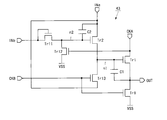
- the shift register according to the present embodiment includes a unit circuit 43 shown in FIG. 30 instead of the unit circuit 41.
- the unit circuit 43 is obtained by adding an N-channel transistor Tr8 to the unit circuit 42 (FIG. 29).
- the drain terminal of the transistor Tr8 is connected to the output terminal OUT, the low level potential VSS is applied to the source terminal of the transistor Tr8, and the gate terminal of the transistor Tr8 is connected to the clock terminal CKB.
- the signal waveform diagram of the shift register according to the present embodiment is the same as the signal waveform diagram shown in FIG.
- the transistor Tr8 can be used to reliably set the output signal OUT to the low level after the transistor Tr1 is turned off. Therefore, according to the shift register of this embodiment, the operation margin can be increased.
- the output signal OUT cannot be kept at a low level due to an off-leakage current of the transistor Tr1 or a leakage current in a circuit connected to the output terminal OUT, and the shift register may malfunction.
- the output signal OUT is periodically set to a low level using the transistor Tr8. Therefore, according to the shift register according to the present embodiment, it is possible to prevent malfunction caused by the potential increase of the output signal OUT.
- the transistor Tr13 is turned on, and a current flows from the node n1 toward the input terminal INa. This current flows into the output terminal OUT of the unit circuit 43 in the preceding stage.
- the clock signal CKB is at the high level, and the transistor Tr8 is in the ON state. For this reason, the current flowing into the output terminal OUT flows to the terminal having the low level potential VSS via the transistor Tr8. Therefore, according to the shift register according to the present embodiment, it is possible to prevent electric charge from staying at the output terminal of the unit circuit and increase the operation margin.
- the shift register according to the fourteenth embodiment of the present invention has the configuration shown in FIG.
- the shift register according to the present embodiment includes a unit circuit 44 shown in FIG.
- the unit circuit 44 is obtained by removing the capacitor C1 from the unit circuit 43 (FIG. 30) and adding an N-channel transistor Tr14.
- the drain terminal of the transistor Tr14 is connected to the gate terminal of the transistor Tr1, the source terminal of the transistor Tr14 is connected to the output terminal OUT, and the gate terminal of the transistor Tr14 is connected to the clock terminal CKA.
- the signal waveform diagram of the shift register according to the present embodiment is the same as the signal waveform diagram shown in FIG.
- the unit circuit 41 (FIG. 26) when the clock signal CKA changes from low level to high level, the potential of the node n1 rises due to the parasitic capacitance between the gate and drain of the transistor Tr1, and the transistor Tr1 is turned on and shifted. Registers may malfunction.
- a unit circuit 42 (FIG. 29) including a capacitor C1 as in the twelfth embodiment.
- this method increases the circuit layout area by the amount of the capacitor C1.
- the unit circuit 44 includes a transistor Tr14.
- the unit circuit 44 when the clock signal CKA is at a high level, the transistor Tr14 is turned on, and the node n1 and the output terminal OUT are electrically connected via the transistor Tr14. For this reason, since the ratio of the parasitic capacitance of the transistor Tr1 to the entire capacitance associated with the node n1 and the output terminal OUT is decreased, the unit circuit 44 is not easily affected by noise from the clock signal CKA. Therefore, according to the shift register of the present embodiment, it is possible to prevent malfunction caused by a change in the clock signal.
- the transistor Tr14 when the output signal OUT is at a high level, the transistor Tr14 is turned off, so that no current flows through the transistor Tr14 from the node n1 toward the output terminal OUT. Therefore, since the potential of the node n1 rises due to the push-up, the high level potential VDD without a threshold drop can be output as the output signal OUT.
- a unit circuit to which the transistor Tr14 is added without deleting the capacitor C1 from the unit circuit 43 may be used.
- FIG. 32 is a block diagram showing a configuration of a shift register according to the fifteenth embodiment of the present invention.
- the shift register 50 shown in FIG. 32 is configured by connecting n unit circuits 51 in multiple stages.
- the unit circuit 51 has clock terminals CKA and CKB, input terminals INa and INb, an initialization terminal INIT, and an output terminal OUT.
- the shift register 50 is supplied with start pulses STa and STb, four-phase clock signals CK1 to CK4, and an initialization signal INIT from the outside.
- the initialization signal INIT is supplied to the initialization terminals INIT of the n unit circuits 51.
- Other signals are supplied to the respective terminals in the same manner as the shift register 40 (FIG. 25) according to the eleventh embodiment.
- FIG. 33 is a circuit diagram of the unit circuit 51.
- the unit circuit 51 is obtained by adding N-channel transistors Tr15 to Tr17 to the unit circuit 44 (FIG. 31).
- the drain terminals of the transistors Tr15 to Tr17 are connected to the gate terminal of the transistor Tr2, the gate terminal of the transistor Tr1, and the output terminal OUT, respectively.
- the low level potential VSS is applied to the source terminals of the transistors Tr15 to Tr17, and the gate terminals of the transistors Tr15 to Tr17 are connected to the initialization terminal INIT.
- the signal waveform diagram during operation of the shift register according to the present embodiment is the same as the signal waveform diagram shown in FIG.
- the initialization signal INIT is controlled to a high level immediately after the power is turned on, when the power is turned off, when the shift register is temporarily set to the initial state, etc., and is controlled to a low level otherwise.
- the initialization signal INIT is at a low level
- the transistors Tr15 to Tr17 are turned off, and the unit circuit 51 operates in the same manner as the unit circuit 44.
- the initialization signal INIT is at a high level
- the transistors Tr15 to Tr17 are turned on.
- the potential of the node n2 is initialized to a low level.
- the transistor Tr16 is turned on, the potential of the node n1 is initialized to a low level.
- the output signal OUT is initialized to a low level.
- the potentials of the nodes n1 and n2 and the output signal OUT can be initialized to a low level using the transistors Tr15 to Tr17.
- the shift register according to the sixteenth embodiment of the present invention has the configuration shown in FIG.
- the shift register according to the present embodiment includes a unit circuit 52 shown in FIG. 34 instead of the unit circuit 51.
- the connection destination of the source terminals of the transistors Tr12 and Tr15 is changed to the input terminal INb, and the connection destination of the source terminal of the transistor Tr16 is changed to the output terminal OUT.
- the signal waveform diagram during operation of the shift register according to the present embodiment is the same as the signal waveform diagram shown in FIG.
- the transistors Tr15 to Tr17 are turned off, and the unit circuit 52 operates in the same manner as the unit circuit 44 (FIG. 31).
- the clock signal CKA changes to high level at time t4 shown in FIG. 28, the transistor Tr12 is turned on.
- the input signal INb is at a low level, a current passing through the transistor Tr12 flows from the node n2 toward the input terminal INb, and the potential of the node n2 drops to a low level (discharge of the node n2). For this reason, the transistor Tr2 is turned off.
- the transistors Tr15 to Tr17 are turned on.
- the output signal OUT is initialized to a low level.
- the gate terminal of the transistor Tr1 is electrically connected to the output terminal OUT via the transistor Tr16.
- the potential of the node n1 is initialized to the low level.
- the transistor Tr15 is turned on, the gate terminal of the transistor Tr2 is electrically connected to the input terminal INb via the transistor Tr15.
- the input signal INb (the output signal OUT of the unit circuit 52 two stages before) is at the low level, so the potential at the node n2 is initialized to the low level. Further, by controlling the start pulses STa and STb to the low level at the time of initialization, the potential of the node n2 can be initialized to the low level also for the first-stage and second-stage unit circuits 52. Therefore, according to the shift register of this embodiment, initialization similar to that of the fifteenth embodiment can be performed.
- the transistor when a high voltage is applied between the source and the drain of the transistor, the transistor may be deteriorated or destroyed. Therefore, as a countermeasure against withstand voltage, a method using a plurality of transistors connected in series or a transistor with a long L length is conventionally known. However, the conventional withstand voltage countermeasure has a problem that the circuit layout area increases.
- the potentials of the nodes n1 and n2 reach the maximum (VDD ⁇ Vth + ⁇ ) by pushing up. Since the potential of the output signal OUT is VDD during the push-up period of the node n1, a voltage ( ⁇ Vth) is applied between the source and drain of the transistor Tr16. In many parts of the push-up period of the node n2 (time t2 to t3 shown in FIG. 28), the potential of the input signal INb is VDD, so that the same voltage ( ⁇ Vth) is applied. The voltage ( ⁇ Vth) is lower than the driving voltage of the transistor.
- the potential of the node n2 becomes (VDD ⁇ Vth + ⁇ ), and the clock signal CKB becomes low level.
- a high voltage (VDD ⁇ Vth + ⁇ VSS) is applied between the source and drain of the transistors Tr12 and Tr15.
- the duty ratio of the clock signals CK1 to CK4 should be 50%, and the high level period of the start pulses STa and STb should be the same length as the high level period of the clock signals CK1 to CK4.
- the source terminals of the transistors Tr12 and Tr15 may be connected to other terminals (for example, the clock terminal CKB) that are at a low level at initialization and are at a high level when the node n2 is pushed up. It may be connected to another terminal (for example, a clock terminal CKA) that is at a low level at the time of initialization and at a high level when the node n1 is pushed up. Even if such a unit circuit is used, the same effect as in the present embodiment can be obtained.
- the shift register according to the seventeenth embodiment of the present invention has the configuration shown in FIG.
- the shift register according to the present embodiment includes a unit circuit 53 shown in FIG. 35 instead of the unit circuit 51.
- the unit circuit 53 is obtained by adding an N-channel transistor Tr18 to the unit circuit 52 (FIG. 34).
- the drain terminal of the transistor Tr18 is connected to the source terminal of the transistor Tr2, the source terminal of the transistor Tr18 is connected to the gate terminal of the transistor Tr1, and the high level potential VDD is applied to the gate terminal of the transistor Tr18.
- the transistor Tr18 functions as a withstand voltage transistor.
- n8 the node to which the drain terminal of the transistor Tr18 is connected
- n9 the node to which the source terminal of the transistor Tr18 is connected
- FIG. 36 is a signal waveform diagram of the shift register according to the present embodiment.
- the signal waveform diagram shown in FIG. 36 is obtained by deleting the potential change at the node n1 from the signal waveform diagram shown in FIG. 28 and adding the potential change at the nodes n8 and n9.
- the voltage between the terminals of the transistors Tr2, Tr13, and Tr16 is lower than the driving voltage of the transistor even during the push-up period of the node n9. Is given. Therefore, according to the shift register of this embodiment, it is possible to prevent the transistor from being deteriorated or destroyed. Similarly to the sixth embodiment, the operation margin can be increased while preventing the transistor from being deteriorated or broken as compared with the case where the withstand voltage measure is taken for the unit circuit not including the transistor Tr11.
- the shift register according to the eighteenth embodiment of the present invention has the configuration shown in FIG.
- the shift register according to the present embodiment includes a unit circuit 54 shown in FIG.
- the unit circuit 54 is obtained by changing the connection destination of the gate terminal of the transistor Tr12 to the output terminal OUT in the unit circuit 52 (FIG. 34).
- the signal waveform diagram of the shift register according to the present embodiment is the same as the signal waveform diagram shown in FIG. Prior to time t4, the unit circuit 54 operates in the same manner as the unit circuit 52.
- the clock signal CKA changes from the low level to the high level at time t4
- the high level potential of the clock signal CKA is output as the output signal OUT after time t4.
- the transistor Tr12 is turned on.
- the input signal INb is at a low level
- the potential of the node n2 falls and becomes a low level (discharge of the node n2). For this reason, the transistor Tr2 is turned off.
- the gate terminal of the transistor Tr12 is connected to the clock terminal CKA.
- the gate terminal of the transistor Tr12 is connected to the output terminal OUT.
- the frequency with which the output signal OUT changes is less than the frequency with which the clock signal CKA changes. Therefore, according to the shift register according to the present embodiment, charging / discharging of the parasitic capacitance associated with the gate terminal of the transistor Tr12 can be reduced, and power consumption can be reduced.
- the shift register according to the nineteenth embodiment of the present invention has the configuration shown in FIG.
- the shift register according to the present embodiment includes a unit circuit 55 shown in FIG. 38 instead of the unit circuit 51.
- the unit circuit 55 is obtained by changing the connection destination of the drain terminal of the transistor Tr11 to the clock terminal CKB in the unit circuit 52 (FIG. 34).
- the signal waveform diagram of the shift register according to the present embodiment is the same as the signal waveform diagram shown in FIG.
- the potentials of the nodes n1 and n2 and the output signal OUT are at a low level.
- the transistor Tr11 is turned on, a current passing through the transistor Tr11 flows from the clock terminal CKB toward the node n2, and the potential of the node n2 rises (node n2 charge).
- the transistor Tr11 is turned off, the node n2 is in a floating state, and the transistors Tr2 and Tr13 are turned on.
- the unit circuit 55 operates in the same manner as the unit circuit 44 (FIG. 31). According to the shift register of this embodiment, the same effect as that of the shift register of the sixteenth embodiment can be obtained.
- the on-potential output unit (input terminal INa) outputs the first input signal INa to the unit circuit 41, and the set control unit receives the second clock signal CKB at the first conduction terminal.
- the second conduction terminal is connected to the control terminal of the set transistor Tr2, and the control terminal includes the transistor Tr11 to which the second input signal INb for the unit circuit 55 is given.
- the potential of the control terminal of the set transistor Tr2 When the potentials of the second input signal INb and the second clock signal CKB change to the on potential (high level potential), the potential of the control terminal of the set transistor Tr2 reaches a predetermined level (VDD ⁇ Vth), and then the set transistor Tr2 The control terminal is in a floating state. Thereafter, when the potential of the first input signal INa changes to the on potential and the potential of the control terminal of the output transistor Tr1 changes to the on potential, the potential of the control terminal of the set transistor Tr2 becomes a sufficient on potential (normal high level potential). And the potential of the control terminal of the output transistor Tr1 becomes the ON potential VDD with no threshold drop.
- the shift register of this embodiment it is possible to reduce the rounding of the output signal OUT and increase the operation margin with respect to the change in the threshold voltage of the transistor. Further, after the potential of the control terminal of the set transistor Tr2 is changed to the on potential based on the second input signal INb and the second clock signal CKB, the potential of the control terminal of the output transistor Tr1 is changed to the on potential based on the first input signal INa. By changing to, the operating margin can be increased.
- the shift register according to the twentieth embodiment of the present invention has the configuration shown in FIG.
- the shift register according to the present embodiment includes a unit circuit 56 shown in FIG. 39 instead of the unit circuit 51.
- the unit circuit 56 is obtained by changing the connection destination of the gate terminal of the transistor Tr11 to the clock terminal CKB in the unit circuit 52 (FIG. 34).
- the signal waveform diagram of the shift register according to the present embodiment is the same as the signal waveform diagram shown in FIG.
- the potential of the node n2 Prior to time t1, the potential of the node n2 is at a low level.
- the transistor Tr11 When the input signal INb and the clock signal CKB change to high level at time t1, the transistor Tr11 is turned on, a current passing through the transistor Tr11 flows from the input terminal INb toward the node n2, and the potential of the node n2 rises (node n2 charge).
- the transistor Tr11 is turned off, the node n2 is in a floating state, and the transistors Tr2 and Tr13 are turned on.
- the unit circuit 56 operates in the same manner as the unit circuit 44 (FIG. 31).
- the transistor Tr11 when the clock signal CKB is at a high level, the transistor Tr11 is turned on. Even when the transistor Tr11 is turned on, the potential of the node n2 is kept low while the input signal INb is low. According to the shift register of this embodiment, the same effect as that of the shift register of the sixteenth embodiment can be obtained.
- the ON potential output unit (input terminal INa) outputs the first input signal INa for the unit circuit 41
- the set control unit outputs the second input signal for the unit circuit 56 to the first conduction terminal.
- the transistor includes a transistor Tr11 to which INb is applied, a second conduction terminal is connected to a control terminal of the set transistor Tr2, and a second clock signal CKB is applied to the control terminal. According to the shift register of this embodiment, as in the nineteenth embodiment, it is possible to reduce the rounding of the output signal OUT and increase the operation margin with respect to fluctuations in the threshold voltage of the transistor.
- the potential of the control terminal of the set transistor Tr2 is changed to the on potential based on the second input signal INb and the second clock signal CKB
- the potential of the control terminal of the output transistor Tr1 is changed to the on potential based on the first input signal INa.
- the shift register according to the twenty-first embodiment of the present invention has the configuration shown in FIG.
- the shift register according to the present embodiment includes a unit circuit 57 shown in FIG. 40 instead of the unit circuit 51.
- the unit circuit 57 is obtained by removing the transistor Tr12 from the unit circuit 52 (FIG. 34) and applying a high level potential VDD to the gate terminal of the transistor Tr11.
- the transistors Tr1, Tr2, and Tr11 function as an output transistor, a set transistor, and a set control unit, respectively, and the input terminal INa functions as an on-potential output unit.
- FIG. 41 is a signal waveform diagram of the shift register according to the present embodiment.
- the signal waveform diagram shown in FIG. 41 is the same as the signal waveform diagram shown in FIG. 28 except for the change in potential of the node n2.
- the potentials of the nodes n1 and n2 and the output signal OUT are at a low level.
- the transistor Tr11 is turned on, a current passing through the transistor Tr11 flows from the input terminal INb toward the node n2, and the potential of the node n2 rises (charge of the node n2). .
- the transistor Tr11 is turned off, the node n2 is in a floating state, and the transistors Tr2 and Tr13 are turned on.
- the unit circuit 57 operates in the same manner as the unit circuit 44 (FIG. 31). According to the shift register of this embodiment, the same effect as that of the shift register of the sixteenth embodiment can be obtained.
- the on-potential output unit (input terminal INa) outputs the first input signal INa for the unit circuit 41
- the set control unit outputs the second input signal for the unit circuit 57 to the first conduction terminal.
- the transistor includes a transistor Tr11 to which INb is applied, the second conduction terminal is connected to the control terminal of the set transistor Tr2, and the ON potential VDD is fixedly applied to the control terminal. According to the shift register of this embodiment, as in the eleventh embodiment, it is possible to reduce the rounding of the output signal OUT and increase the operation margin with respect to fluctuations in the threshold voltage of the transistor.
- the potential of the control terminal of the set transistor Tr2 is changed to the on potential based on the second input signal INb.
- the operating margin can be increased.
- FIG. 42 is a block diagram showing a configuration of a shift register according to the twenty-second embodiment of the present invention.
- the shift register 60 shown in FIG. 42 is configured by connecting n unit circuits 61 in multiple stages.
- the unit circuit 61 has clock terminals CKA and CKB, an input terminal INa, an initialization terminal INIT, and an output terminal OUT.
- the shift register 60 is supplied with a start pulse STa, four-phase clock signals CK1 to CK4, and an initialization signal INIT from the outside.
- the clock signals CK1 to CK4 are given to the respective terminals similarly to the shift register 40 (FIG. 25) according to the eleventh embodiment.
- the initialization signal INIT is supplied to the initialization terminals INIT of the n unit circuits 61.
- the start pulse STa is given to the input terminal INa of the first stage unit circuit 61.
- the output signal OUT of the unit circuit 61 is output to the outside as output signals O1 to On, and is given to the input terminal INa of the unit circuit 61 at the next stage.
- FIG. 43 is a circuit diagram of the unit circuit 61.
- the unit circuit 61 is obtained by changing the connection destination of the gate terminal and drain terminal of the transistor Tr11 and the source terminals of the transistors Tr12 and Tr15 to the clock terminal CKB in the unit circuit 52 (FIG. 34).
- FIG. 44 is a signal waveform diagram of the shift register 60.
- FIG. The signal waveform diagram shown in FIG. 44 has the exception that the change in potential of the input signal INb is deleted and that the potential of the node n2 periodically becomes a predetermined level (VDD ⁇ Vth) after time t7. It is the same as the signal waveform diagram shown in FIG. Prior to time t1, the potentials of the nodes n1 and n2 and the output signal OUT are at a low level.
- the clock signal CKB changes to high level at time t1
- the transistor Tr11 is turned on, a current passing through the transistor Tr11 flows from the clock terminal CKB toward the node n2, and the potential of the node n2 rises (charge of the node n2). .
- both the transistors Tr2 and Tr13 are turned on.
- the unit circuit 61 operates in the same manner as the unit circuit 44 (FIG. 31).
- the transistor Tr13 When the clock signal CKB changes to high level at time t7, the transistor Tr13 is turned on and the node n1 is discharged. At time t7, the transistor Tr11 is turned on. For this reason, a current passing through the transistor Tr11 flows from the clock terminal CKB toward the node n2, and the potential of the node n2 rises. After time t7, the potential of the node n2 changes to (VDD ⁇ Vth) when the clock signal CKB changes to high level, and changes to low level when the clock signal CKA changes to high level.
- the shift register 60 it is not necessary to supply the start pulse STb to the shift register 60, and it is not necessary to supply the output signal OUT of the unit circuit 61 two stages before to the unit circuit 61. Therefore, according to the shift register 60 according to the present embodiment, the wiring between unit circuits can be reduced, and the layout area of the circuit can be reduced.
- the ON potential output unit (input terminal INa) outputs the input signal INa to the unit circuit 41, and the set control unit applies the second clock signal CKB to the first conduction terminal and the control terminal.
- the second conduction terminal includes the transistor Tr11 connected to the control terminal of the set transistor Tr2.
- the shift register of this embodiment it is possible to reduce the rounding of the output signal OUT and increase the operation margin with respect to the change in the threshold voltage of the transistor.
- the potential of the control terminal of the set transistor Tr2 is changed to the on potential based on the second clock signal CKB
- the potential of the control terminal of the output transistor Tr1 is changed to the on potential based on the input signal INa. Can be increased.
- the shift register according to the twenty-third embodiment of the present invention has the configuration shown in FIG.
- the shift register according to the present embodiment includes a unit circuit 62 shown in FIG. 45 instead of the unit circuit 61.
- the unit circuit 62 is obtained by changing the connection destination of the gate terminal of the transistor Tr12 to the output terminal OUT in the unit circuit 61 (FIG. 43).
- FIG. 46 is a signal waveform diagram of the shift register according to the present embodiment.
- the signal waveform diagram shown in FIG. 46 is the same as the signal waveform diagram shown in FIG. 44 except for the change in potential of the node n2.
- the potential of the node n1 and the output signal OUT Prior to time t2, the potential of the node n1 and the output signal OUT are at a low level, the potential of the node n2 is (VDD ⁇ Vth), the node n2 is in a floating state, and the transistor Tr2 is in an on state.
- the input signal INa changes to a low level.
- the transistors Tr2 and Tr13 are off, the potentials of the nodes n1 and n2 do not change.
- the clock signal CKA changes to low level at time t6
- the output signal OUT changes to low level
- the transistor Tr12 is turned off.
- the potential of the node n1 falls to the high level potential VDD.
- the clock signal CKB changes to high level at time t7
- the node n1 is discharged.
- the transistor Tr11 is turned on, so that the potential of the node n2 rises to (VDD ⁇ Vth) (charge of the node n2).
- charging / discharging of the parasitic capacitance associated with the gate terminal of the transistor Tr12 can be reduced, and power consumption can be reduced. Further, the node n2 is discharged only when the output signal OUT is at a high level. Therefore, according to the shift register according to the present embodiment, charging / discharging of the parasitic capacitance associated with the node n2 can be reduced, and power consumption can be reduced.
- FIG. 47 is a block diagram showing a configuration of a shift register according to the twenty-fourth embodiment of the present invention.
- the shift register 70 shown in FIG. 47 has n unit circuits 71 connected in multiple stages and a dummy unit circuit 72 connected in the preceding stage.
- the unit circuit 71 has clock terminals CKA and CKB, input terminals INa and INb, an initialization terminal INIT, and an output terminal OUT.
- the dummy unit circuit 72 has clock terminals CKA and CKB, an input terminal INa, an initialization terminal INIT, and an output terminal OUT.
- the unit circuit 52 (FIG. 34) is used for the unit circuit 71
- the unit circuit 61 (FIG. 43) is used for the dummy unit circuit 72.
- the shift register 70 is supplied with a start pulse STa, four-phase clock signals CK1 to CK4, and an initialization signal INIT from the outside.
- the clock signals CK1 to CK4 are given to the respective terminals similarly to the shift register 40 (FIG. 25) according to the eleventh embodiment.
- the clock signal CK2 is supplied to the clock terminal CKB of the dummy unit circuit 72
- the clock signal CK4 is supplied to the clock terminal CKA of the dummy unit circuit 72.
- the start pulse STa is applied to the input terminal INa of the dummy unit circuit 72 and the input terminal INb of the unit circuit 71 in the first stage.
- the initialization signal INIT is supplied to the initialization terminals INIT of the n unit circuits 71 and the dummy unit circuit 72.
- the output signal OUT of the dummy unit circuit 72 is supplied to the input terminal INa of the first stage unit circuit 71 and the input terminal INb of the second stage unit circuit 71 without being output to the outside.
- the output signal OUT of the unit circuit 71 is output to the outside as output signals O1 to On, and is also supplied to the input terminal INa of the next stage unit circuit 71 and the input terminal INb of the unit circuit 71 of the second stage.
- FIG. 48 is a timing chart of the shift register 70.
- the start pulse STa and the clock signals CK1 to CK4 change at the same timing as in the eleventh embodiment (see FIG. 27).
- the output signal OUT of the dummy unit circuit 72 (hereinafter referred to as a dummy output signal Odmy) is a signal obtained by delaying the start pulse STa by a quarter cycle of the clock signal CK1.
- the start pulse STa and the dummy output signal Odmy have the same role as the start pulses STb and STa in the shift register 40 according to the eleventh embodiment, respectively.
- the shift register 70 includes the dummy unit circuit 72 that outputs a signal obtained by delaying the start pulse STa by 1 ⁇ 4 period of the clock signal. Therefore, only one start pulse is supplied to the shift register 70. Therefore, according to the shift register 70 according to the present embodiment, the layout area can be reduced by the amount of the input terminal that supplies the start pulse and the wiring that propagates the start pulse.
- FIG. 49 is a block diagram showing a configuration of the shift register according to the twenty-fifth embodiment of the present invention.
- the shift register 80 shown in FIG. 49 is configured by connecting n unit circuits 81 and two dummy unit circuits 82 and 83 in multiple stages.
- the unit circuit 81 has clock terminals CKA and CKB, input terminals INa and INb, an initialization terminal INIT, a reset terminal R, and an output terminal OUT.
- the dummy unit circuits 82 and 83 have clock terminals CKA and CKB, input terminals INa and INb, an initialization terminal INIT, and an output terminal OUT.
- the shift register 80 is supplied with start pulses STa and STb, four-phase clock signals CK1 to CK4, and an initialization signal INIT from the outside.
- the start pulses STa and STb and the clock signals CK1 to CK4 are given to the respective terminals similarly to the shift register 40 (FIG. 25) according to the eleventh embodiment.
- the clock signals CK1 to CK4 are supplied to the clock terminal CKA of the dummy unit circuit 82, the clock terminal CKA of the dummy unit circuit 83, the clock terminal CKB of the dummy unit circuit 82, and the clock terminal of the dummy unit circuit 83, respectively. Given to CKB.
- the initialization signal INIT is supplied to the initialization terminals INIT of the n unit circuits 81 and the dummy unit circuits 82 and 83.
- the output signal OUT of the unit circuit 81 is output to the outside as output signals O1 to On, and the input circuit INa of the next stage unit circuit 81 (or dummy unit circuit 82), the unit circuit 81 after 2 stages (or , The input terminal INb of the dummy unit circuits 82 and 83) and the reset terminal R of the unit circuit 81 two stages before.
- An output signal OUT of the dummy unit circuit 82 (hereinafter referred to as a dummy output signal Odmy1) is supplied to the input terminal INa of the dummy unit circuit 83 and the reset terminal R of the unit circuit 81 in the (n ⁇ 1) th stage.
- An output signal OUT of the dummy unit circuit 83 (hereinafter referred to as a dummy output signal Odmy2) is supplied to the reset terminal R of the n-th unit circuit 81.
- FIG. 50 is a circuit diagram of the unit circuit 81.
- the unit circuit 81 is obtained by changing the connection destination of the gate terminal of the transistor Tr13 to the reset terminal R in the unit circuit 54 (FIG. 37).
- a unit circuit for example, the unit circuit 54 that does not have the reset terminal R is used.
- the node n1 is discharged using the transistor Tr13 to which the output signal OUT of the unit circuit 81 after two stages is applied to the gate terminal.
- the shift register 80 includes dummy unit circuits 82 and 83 in order to give the output signal OUT of the unit circuit 81 after the second stage to the (n ⁇ 1) -th and n-th unit circuits 81.
- a dummy output signal Odmy1 is supplied to the gate terminal of the transistor Tr13 of the unit circuit 81 in the (n ⁇ 1) th stage.
- a dummy output signal Odmy2 is supplied to the gate terminal of the transistor Tr13 of the n-th unit circuit 81.
- FIG. 51 is a signal waveform diagram of the shift register 80.
- the signal waveform diagram shown in FIG. 51 is obtained by adding a change in the reset signal R to the signal waveform diagram shown in FIG.
- the output signal OUT changes to a high level at time t4 and changes to a low level at time t6.
- the reset signal R changes to a high level at a time t7 and changes to a low level at a time t8 after a half cycle of the clock signal CK1.
- the clock signal CKA changes to the low level at time t6, the pushing up of the node n1 is finished, and the potential of the node n1 falls to the high level potential VDD.
- the reset signal R changes to high level at time t7, the transistor Tr13 is turned on, and the potential of the node n1 drops to low level (discharge of the node n1).
- the transistor Tr13 when the clock signal CKB is at a high level, the transistor Tr13 is turned on and the node n1 is discharged.
- the unit circuit 81 when the reset signal R is at a high level, the transistor Tr13 is turned on and the node n1 is discharged.
- the frequency with which the reset signal R changes is less than the frequency with which the clock signal CKB changes. Therefore, according to the shift register 80 according to the present embodiment, charging / discharging of the parasitic capacitance associated with the gate terminal of the transistor Tr13 can be reduced, and power consumption can be reduced.
- the shift register 80 can be configured as a modification shown in FIG.
- the shift register 84 shown in FIG. 52 is configured by connecting (n + 2) unit circuits 81 in multiple stages.
- the unit circuit 81 at the (n + 1) stage and the (n + 2) stage functions as a dummy unit circuit.
- the shift register 84 is supplied with start pulses STa and STb, four-phase clock signals CK1 to CK4, an initialization signal INIT, and a reset signal R from the outside.
- the reset signal R is given to the reset terminal R of the unit circuit 81 at the (n + 1) th stage and the (n + 2) th stage. Other signals are applied to the respective terminals in the same manner as the shift register 80.
- the shift register 84 similarly to the shift register 80, the node n1 is discharged using the transistor Tr13 to which the output signal OUT of the unit circuit 81 after two stages is applied to the gate terminal.
- the shift register 84 supplies the unit circuit 81 of the (n + 1) th stage and the nth stage. I have.
- the gate terminal of the transistor Tr13 of the (n ⁇ 1) th stage unit circuit 81 is supplied with the output signal OUT (hereinafter referred to as a dummy output signal Odmy1) of the (n + 1) th stage unit circuit 81.
- An output signal OUT (hereinafter referred to as a dummy output signal Odmy2) of the (n + 2) -th unit circuit 81 is supplied to the gate terminal of the transistor Tr13 of the n-th unit circuit 81.
- FIG. 53 is a timing chart of the shift register 84.
- the dummy output signal Odmy1 becomes high level during the high level period of the clock signal CK1 after the output signal OUT of the n-th unit circuit 81 becomes high level.
- the dummy output signal Odmy2 becomes high level during the high level period of the clock signal CK2 after the dummy output signal Odmy1 becomes high level.
- the reset signal R becomes high level after the high level period of the dummy output signal Odmy2.
- the transistor Tr13 is turned on, and the potential of the node n1 becomes low level.
- the shift register 84 can reduce charging / discharging of the parasitic capacitance associated with the gate terminal of the transistor Tr13, thereby reducing power consumption.
- the shift register 84 may be supplied with a control signal that becomes a high level at the time of initialization and reset. In this case, one of the transistors Tr13 and Tr16 may be deleted from the unit circuit 81.
- the shift register according to the twenty-sixth embodiment of the present invention has the configuration shown in FIG. 49 or FIG.
- the shift register according to this embodiment includes a unit circuit 85 shown in FIG.
- the unit circuit 85 is obtained by adding a transistor Tr19 to the unit circuit 81 (FIG. 50).
- the drain terminal of the transistor Tr19 is connected to the output terminal OUT, the low level potential VSS is applied to the source terminal of the transistor Tr19, and the gate terminal of the transistor Tr19 is connected to the reset terminal R.
- the signal waveform diagram of the shift register according to this embodiment is the same as the signal waveform diagram according to the twenty-fifth embodiment.
- the unit circuit 43 (FIG. 30) includes a transistor Tr8 whose gate terminal is connected to the clock terminal CKB in order to set the output signal OUT to a low level.
- the unit circuit 85 includes a transistor Tr19 having a gate terminal connected to the reset terminal R.
- the output signal OUT when the reset signal R becomes high level, the transistor Tr19 is turned on, so that the output signal OUT is surely low level. Therefore, in the unit circuit 85, it is not necessary to increase the size of the transistor Tr8.
- the frequency with which the output signal OUT changes is less than the frequency with which the clock signal CKB changes. For this reason, even if the size of the transistor Tr19 is increased, the power consumption is not increased as the transistor Tr8 is increased. Therefore, according to the shift register of the present embodiment, the output signal OUT can be reliably set to a low level without increasing power consumption.
- the transistor Tr8 is periodically turned on based on the clock signal CKB. Therefore, even if the potential of the output signal OUT rises due to the leakage current of the transistor Tr1, etc., the potential of the output signal OUT can be periodically lowered to a low level using the transistor Tr8.
- the unit circuit 85 includes the transistors Tr8 and Tr19, the transistor Tr8 is not necessarily included when the transistor Tr19 is included.
- FIG. 55 is a block diagram showing a first configuration example of the liquid crystal display device including the shift register according to the embodiment of the present invention.
- the liquid crystal display device shown in FIG. 55 includes n scanning lines GL1 to GLn, m (m is an integer of 2 or more) data lines SL1 to SLm, (m ⁇ n) pixel circuits 101, and a data line driving circuit.
- 111 and shift registers 121 and 122 are provided.
- the scanning lines GL1 to GLn are arranged in parallel to each other, and the data lines SL1 to SLm are arranged in parallel to each other so as to be orthogonal to the scanning lines GL1 to GLn.
- the (m ⁇ n) pixel circuits 101 are arranged corresponding to the intersections of the scanning lines GL1 to GLn and the data lines SL1 to SLm.
- the pixel circuit 101 includes a transistor Tw, a liquid crystal capacitor Clc, and an auxiliary capacitor Ccs.
- the gate terminal of the transistor Tw is connected to one scanning line, and the source terminal of the transistor Tw is connected to one data line.
- the arrangement area of the pixel circuit 101 is referred to as an area A.
- the data line driving circuit 111 is arranged along one side (the upper side in FIG. 55) of the region A.
- the data line driving circuit 111 is connected to one end (the upper end in FIG. 55) of the data lines SL1 to SLm, and drives the data lines SL1 to SLm.
- the shift registers 121 and 122 each have n output terminals O1 to On and function as a scanning line driving circuit.
- the shift registers 121 and 122 for example, the shift registers according to the first to tenth embodiments are used. The same circuit is used for the shift registers 121 and 122, and the same signals are supplied.
- the shift register 121 is disposed along one side of the region A (left side in FIG. 55), and the shift register 122 is disposed along the opposite side of the region A (right side in FIG. 55).
- the output terminals O1 to On of the shift register 121 are connected to one end (the left end in FIG. 55) of the scanning lines GL1 to GLn, respectively.
- the shift register 121 drives the scanning lines GL1 to GLn from one end side.
- the output terminals O1 to On of the shift register 122 are connected to the other ends (right end in FIG. 55) of the scanning lines GL1 to GLn, respectively.
- the shift register 122 drives the scanning lines GL1 to GLn from the other end side. In this manner, in the liquid crystal display device shown in FIG. 55, the scanning lines GL1 to GLn are driven from both sides using the two shift registers 121 and 122.
- FIG. 56 is a block diagram showing a second configuration example of the liquid crystal display device including the shift register according to the embodiment of the present invention.
- the liquid crystal display device shown in FIG. 56 is obtained by replacing the shift registers 121 and 122 with shift registers 123 and 124 in the liquid crystal display device shown in FIG.
- Each of the shift registers 123 and 124 has n output terminals O1 to On and functions as a scanning line driving circuit.
- the shift registers 123 and 124 for example, the shift registers according to the eleventh to twenty-sixth embodiments are used.
- the scanning lines GL1 to GLn are driven from both sides by using two shift registers arranged along two opposing sides of the region A.
- the liquid crystal display device including the shift register according to the embodiment of the present invention drives the scanning lines GL1 to GLn from one side by using one shift register arranged along one side of the region A. May be.
- FIG. 57 is a block diagram showing a third configuration example of the liquid crystal display device including the shift register according to the embodiment of the present invention.
- the liquid crystal display device shown in FIG. 57 includes 2n scanning lines GL1 to GL2n, m data lines SL1 to SLm, (m ⁇ 2n) pixel circuits 101, a data line driving circuit 111, and a shift register 121, 122 is provided.
- the scanning lines GL1 to GL2n, the data lines SL1 to SLm, the (m ⁇ 2n) pixel circuits 101, and the data line driving circuit 111 are arranged similarly to the liquid crystal display device shown in FIG.
- the same circuit is used for the shift registers 121 and 122, and different signals are given except for the initialization signal INIT.
- the shift registers 121 and 122 for example, the shift registers according to the first to tenth embodiments are used.
- the output terminals O1 to On of the shift register 121 are respectively connected to one end (left end in FIG. 57) of the odd-numbered scanning lines GL1, GL3,.
- the shift register 121 drives odd-numbered scanning lines GL1, GL3,... GL2n-1 from one end side.
- the output terminals O1 to On of the shift register 122 are connected to the other ends (right ends in FIG. 57) of the even-numbered scanning lines GL2, GL4,.
- the shift register 122 drives even-numbered scanning lines GL2, GL4,... GL2n from the other end side. 57, the odd-numbered scanning lines GL1, GL3,..., GL2n-1 are driven from one end side using the shift register 121, and the even-numbered scanning lines GL2, GL4,. The GL 2 n is driven from the other end side using the shift register 122.
- FIG. 58 is a timing chart of the liquid crystal display device shown in FIG.
- the clock signal CK1L supplied to the shift register 121 becomes a high level and a low level at a predetermined cycle. However, the high level period of the clock signal CK1L is shorter than a quarter cycle of the clock signal CK1L.
- the clock signal CK2L is a signal obtained by delaying the clock signal CK1L by a half cycle.
- the clock signals CK1R and CK2R supplied to the shift register 122 are signals obtained by delaying the clock signal CK1L by 1 ⁇ 4 period and 3 ⁇ 4 period, respectively.
- the start pulse STL supplied to the shift register 121 becomes high level during the high level period of the clock signal CK2R at the start of shifting.
- the start pulse STR supplied to the shift register 122 is a signal obtained by delaying the start pulse STL by a quarter cycle of the clock signal CK1L.
- the high level period of the output signal O1 of the shift register 121 is delayed by a quarter cycle of the clock signal from the high level period of the start pulse STL.
- the high level period of the output signals O2 to On of the shift register 121 is delayed by a half cycle of the clock signal from the high level period of the output signals O1 to On-1 of the shift register 121, respectively.
- the high level period of the output signal O1 of the shift register 122 is delayed by a quarter cycle of the clock signal from the high level period of the output signal O1 of the shift register 121.
- the high level period of the output signals O2 to On of the shift register 122 is delayed by a half cycle of the clock signal from the high level period of the output signals O1 to On-1 of the shift register 122, respectively. Therefore, as shown in FIG. 58, the potentials of the scanning lines GL1 to GL2n become high level in ascending order with a delay of 1 ⁇ 4 period of the clock signal.
- FIG. 59 is a block diagram showing a fourth configuration example of the liquid crystal display device including the shift register according to the embodiment of the present invention.
- the liquid crystal display device shown in FIG. 59 is obtained by replacing the shift registers 121 and 122 with shift registers 123 and 124 in the liquid crystal display device shown in FIG.
- the same circuit is used for the shift registers 123 and 124, and different signals are given except for the initialization signal INIT.
- the shift registers 123 and 124 for example, the shift registers according to the eleventh to twenty-sixth embodiments are used.
- FIG. 60 is a timing chart of the liquid crystal display device shown in FIG.
- the start pulses STaL and STbL and the clock signals CK1L to CK4L supplied to the shift register 123 change at the same timing as the start pulses STa and STb and the clock signals CK1 to CK4 shown in FIG.
- the start pulses STaR and STbR and the clock signals CK1R to CK4R supplied to the shift register 124 change with a delay of 1/8 cycle of the clock signal from the signal supplied to the shift register 123.
- the high level period of the output signal O1 of the shift register 123 is delayed by a quarter cycle of the clock signal from the high level period of the start pulse STaL.
- the high level periods of the output signals O2 to On of the shift register 123 are delayed by 1/4 cycle of the clock signal from the high level period of the output signals O1 to On-1 of the shift register 123, respectively.
- the high level period of the output signal O1 of the shift register 124 is delayed by 1/8 cycle of the clock signal from the high level period of the output signal O1 of the shift register 123.
- the high level period of the output signals O2 to On of the shift register 124 is delayed by a quarter cycle of the clock signal from the high level period of the output signals O1 to On-1 of the shift register 124, respectively. Therefore, as shown in FIG. 60, the potentials of the scanning lines GL1 to GL2n become high level in ascending order with a delay of 1/8 period of the clock signal.
- the shift register according to the first to twenty-sixth embodiments as a scanning line driving circuit, the rounding of the output signal of the scanning line driving circuit is reduced, and the threshold voltage of the transistor is reduced. It is possible to increase the operation margin against fluctuation.
- one unit circuit of the shift register needs to be arranged in a region corresponding to the width of one scanning line.
- one unit circuit of the shift register may be arranged in a region corresponding to the width of two scanning lines. Therefore, according to the liquid crystal display device shown in FIGS.
- the width of the layout area of the shift register provided in the outer peripheral portion of the arrangement area of the pixel circuit can be reduced.
- driving signal lines GL1 to GLn from both sides can further reduce the rounding of the output signal compared to driving from one side.
- the threshold voltage of the transistor is controlled by controlling the control terminal of the set transistor to be in a floating state during a part of the period in which the ON potential is applied to the control terminal of the output transistor. It is possible to increase the operation margin with respect to fluctuations.
- the shift registers according to various modified examples can be configured by arbitrarily combining the characteristics of a plurality of unit circuits as long as they do not contradict their properties.
- the shift register may be configured by deleting the breakdown voltage transistor from the unit circuit including the breakdown voltage transistor and connecting the obtained unit circuits in multiple stages.
- a shift register may be configured by adding a breakdown voltage transistor to a unit circuit not including a breakdown voltage transistor and connecting the obtained unit circuits in multiple stages.
- the shift register of the present invention has a feature that it has a large operation margin with respect to fluctuations in the threshold voltage of the transistor, it can be used for various circuits such as a driver circuit of a display device.
Landscapes
- Engineering & Computer Science (AREA)
- Chemical & Material Sciences (AREA)
- Crystallography & Structural Chemistry (AREA)
- Physics & Mathematics (AREA)
- Computer Hardware Design (AREA)
- General Physics & Mathematics (AREA)
- Theoretical Computer Science (AREA)
- Control Of Indicators Other Than Cathode Ray Tubes (AREA)
- Liquid Crystal Display Device Control (AREA)
- Shift Register Type Memory (AREA)
Abstract
Description
前記単位回路は、
第1導通端子がクロック信号を入力するためのクロック端子に接続され、第2導通端子が前記クロック信号を出力するための出力端子に接続された出力トランジスタと、
前記出力トランジスタの制御端子に与えられるオン電位を出力するオン電位出力部と、
第1導通端子に前記オン電位出力部の出力が与えられ、第2導通端子が前記出力トランジスタの制御端子に接続されたセットトランジスタと、
前記セットトランジスタの制御端子にオン電位とオフ電位を切り換えて印加するセット制御部とを備え、
前記セット制御部は、前記出力トランジスタの制御端子にオン電位が与えられる期間の一部において、前記セットトランジスタの制御端子をフローティング状態に制御することを特徴とする。
前記単位回路は、
第1導通端子がクロック信号を入力するためのクロック端子に接続され、第2導通端子が前記クロック信号を出力するための出力端子に接続された出力トランジスタと、
第1導通端子が第1節点に接続され、第2導通端子が前記出力トランジスタの制御端子に接続され、制御端子にオン電位が固定的に印加された耐圧用トランジスタと、
前記第1節点に与えられるオン電位を出力するオン電位出力部と、
第1導通端子に前記オン電位出力部の出力が与えられ、第2導通端子が前記第1節点に接続されたセットトランジスタと、
前記セットトランジスタの制御端子にオン電位とオフ電位を切り換えて印加するセット制御部とを備え、
前記セット制御部は、前記第1節点にオン電位が与えられる期間の一部において、前記セットトランジスタの制御端子をフローティング状態に制御することを特徴とする。
前記オン電位出力部は、前記単位回路に対する入力信号を出力し、
前記セット制御部は、第1導通端子に第2クロック信号が与えられ、第2導通端子が前記セットトランジスタの制御端子に接続され、制御端子にオン電位が固定的に印加されたトランジスタを含むことを特徴とする。
前記オン電位出力部は、前記単位回路に対する入力信号を出力し、
前記セット制御部は、第1導通端子に前記入力信号が与えられ、第2導通端子が前記セットトランジスタの制御端子に接続され、制御端子にオン電位が固定的に印加されたトランジスタを含むことを特徴とする。
前記オン電位出力部は、オン電位を固定的に出力し、
前記セット制御部は、第1導通端子に前記単位回路に対する入力信号が与えられ、第2導通端子が前記セットトランジスタの制御端子に接続され、制御端子にオン電位が固定的に印加されたトランジスタを含むことを特徴とする。
前記オン電位出力部は、前記単位回路に対する第1入力信号を出力し、
前記セット制御部は、第1導通端子と制御端子に前記単位回路に対する第2入力信号が与えられ、第2導通端子が前記セットトランジスタの制御端子に接続されたトランジスタを含むことを特徴とする。
前記オン電位出力部は、前記単位回路に対する第1入力信号を出力し、
前記セット制御部は、第1導通端子に第2クロック信号が与えられ、第2導通端子が前記セットトランジスタの制御端子に接続され、制御端子に前記単位回路に対する第2入力信号が与えられたトランジスタを含むことを特徴とする。
前記オン電位出力部は、前記単位回路に対する第1入力信号を出力し、
前記セット制御部は、第1導通端子に前記単位回路に対する第2入力信号が与えられ、第2導通端子が前記セットトランジスタの制御端子に接続され、制御端子に第2クロック信号が与えられたトランジスタを含むことを特徴とする。
前記オン電位出力部は、前記単位回路に対する第1入力信号を出力し、
前記セット制御部は、第1導通端子に前記単位回路に対する第2入力信号が与えられ、第2導通端子が前記セットトランジスタの制御端子に接続され、制御端子にオン電位が固定的に印加されたトランジスタを含むことを特徴とする。
前記オン電位出力部は、前記単位回路に対する入力信号を出力し、
前記セット制御部は、第1導通端子と制御端子に第2クロック信号が与えられ、第2導通端子が前記セットトランジスタの制御端子に接続されたトランジスタを含むことを特徴とする。
互いに平行に配置された複数の走査線と、
前記走査線と直交するように互いに平行に配置された複数のデータ線と、
前記走査線および前記データ線の交点に対応して配置された複数の画素回路と、
前記走査線を駆動する走査線駆動回路として、第1または第2の発明に係るシフトレジスタとを備える。
前記単位回路が、第1導通端子がクロック信号を入力するためのクロック端子に接続され、第2導通端子が前記クロック信号を出力するための出力端子に接続された出力トランジスタと、第2導通端子が前記出力トランジスタの制御端子に接続されたセットトランジスタとを含む場合に、
前記セットトランジスタの第1導通端子に対して、前記出力トランジスタの制御端子に与えられるオン電位を出力するステップと、
前記セットトランジスタの制御端子にオン電位とオフ電位を切り換えて印加するステップとを備え、
前記セットトランジスタの制御端子の電位を制御するステップは、前記出力トランジスタの制御端子にオン電位が与えられる期間の一部において、前記セットトランジスタの制御端子をフローティング状態に制御することを特徴とする。
前記単位回路が、第1導通端子がクロック信号を入力するためのクロック端子に接続され、第2導通端子が前記クロック信号を出力するための出力端子に接続された出力トランジスタと、第1導通端子が第1節点に接続され、第2導通端子が前記出力トランジスタの制御端子に接続され、制御端子にオン電位が固定的に印加された耐圧用トランジスタと、第2導通端子が前記第1節点に接続されたセットトランジスタとを含む場合に、
前記セットトランジスタの第1導通端子に対して、前記第1節点に与えられるオン電位を出力するステップと、
前記セットトランジスタの制御端子にオン電位とオフ電位を切り換えて印加するステップとを備え、
前記セットトランジスタの制御端子の電位を制御するステップは、前記第1節点にオン電位が与えられる期間の一部において、前記セットトランジスタの制御端子をフローティング状態に制御することを特徴とする。
図2は、本発明の第1の実施形態に係るシフトレジスタの構成を示すブロック図である。図2に示すシフトレジスタ10は、n個(nは2以上の整数)の単位回路11を多段接続して構成されている。単位回路11は、クロック端子CKA、CKB、入力端子IN、および、出力端子OUTを有する。シフトレジスタ10には外部から、スタートパルスSTと2相のクロック信号CK1、CK2が供給される。スタートパルスSTは、1段目の単位回路11の入力端子INに与えられる。クロック信号CK1は、奇数段目の単位回路11のクロック端子CKAと偶数段目の単位回路11のクロック端子CKBに与えられる。クロック信号CK2は、偶数段目の単位回路11のクロック端子CKAと奇数段目の単位回路11のクロック端子CKBに与えられる。単位回路11の出力信号OUTは、出力信号O1~Onとして外部に出力されると共に、次段の単位回路11の入力端子INに与えられる。
本発明の第2の実施形態に係るシフトレジスタは、図2に示す構成を有する。ただし、本実施形態に係るシフトレジスタは、単位回路11に代えて、図6に示す単位回路12を備えている。単位回路12は、単位回路11(図3)に容量C1、C2を追加したものである。容量C1はトランジスタTr1のゲート-ソース間に設けられ、容量C2はトランジスタTr2のゲート-ドレイン間に設けられる。なお、容量C1、C2のうち一方だけを設けてもよい。
本発明の第3の実施形態に係るシフトレジスタは、図2に示す構成を有する。ただし、本実施形態に係るシフトレジスタは、単位回路11に代えて、図7に示す単位回路13を備えている。単位回路13は、単位回路12(図6)にNチャネル型トランジスタTr4~Tr7と抵抗R1を追加したものである。
本発明の第4の実施形態に係るシフトレジスタは、図2に示す構成を有する。ただし、本実施形態に係るシフトレジスタは、単位回路11に代えて、図9に示す単位回路14を備えている。単位回路14は、単位回路13(図7)にNチャネル型トランジスタTr8を追加したものである。トランジスタTr8のドレイン端子は出力端子OUTに接続され、トランジスタTr8のソース端子にはローレベル電位VSSが印加され、トランジスタTr8のゲート端子は節点n3に接続される。
図10は、本発明の第5の実施形態に係るシフトレジスタの構成を示すブロック図である。図10に示すシフトレジスタ20は、n個の単位回路21を多段接続して構成されている。単位回路21は、クロック端子CKA、CKB、入力端子IN、初期化端子INIT、および、出力端子OUTを有する。シフトレジスタ20には外部から、スタートパルスST、2相のクロック信号CK1、CK2、および、初期化信号INITが供給される。初期化信号INITは、n個の単位回路21の初期化端子INITに与えられる。それ以外の信号は、第1の実施形態に係るシフトレジスタ(図2)と同様に各端子に与えられる。
本発明の第6の実施形態に係るシフトレジスタは、図10に示す構成を有する。ただし、本実施形態に係るシフトレジスタは、単位回路21に代えて、図12に示す単位回路22を備えている。単位回路22は、単位回路21(図11)にNチャネル型トランジスタTr10を追加したものである。トランジスタTr10のドレイン端子はトランジスタTr2のソース端子に接続され、トランジスタTr10のソース端子はトランジスタTr1のゲート端子に接続され、トランジスタTr10のゲート端子にはハイレベル電位VDDが印加される。トランジスタTr10は、耐圧用トランジスタとして機能する。以下、トランジスタTr10のドレイン端子が接続された節点をn4、トランジスタTr10のソース端子が接続された節点をn5という。
図14は、本発明の第7の実施形態に係るシフトレジスタの構成を示すブロック図である。図14に示すシフトレジスタ30は、n個の単位回路31を多段接続して構成されている。単位回路31は、クロック端子CKA、CKB、入力端子IN1、IN2、初期化端子INIT、制御端子UD、UDB(図示せず)、および、出力端子OUTを有する。シフトレジスタ30には外部から、スタートパルスST、2相のクロック信号CK1、CK2、初期化信号INIT、および、制御信号UD、UDB(図示せず)が供給される。クロック信号CK1、CK2は、第1の実施形態に係るシフトレジスタ10(図2)と同様に各端子に与えられる。初期化信号INITと制御信号UD、UDBは、それぞれ、n個の単位回路31の初期化端子INITと制御端子UD、UDBに与えられる。スタートパルスSTは、1段目の単位回路31の入力端子IN1とn段目の単位回路31の入力端子IN2に与えられる。単位回路31の出力信号OUTは、出力信号O1~Onとして外部に出力されると共に、次段の単位回路31の入力端子IN1と前段の単位回路31の入力端子IN2に与えられる。
本発明の第8の実施形態に係るシフトレジスタは、図10に示す構成を有する。ただし、本実施形態に係るシフトレジスタは、単位回路21に代えて、図20に示す単位回路23を備えている。単位回路23は、単位回路22(図12)について、トランジスタTr3のドレイン端子の接続先を入力端子INに変更したものである。
本発明の第9の実施形態に係るシフトレジスタは、図10に示す構成を有する。ただし、本実施形態に係るシフトレジスタは、単位回路21に代えて、図22に示す単位回路24を備えている。単位回路24は、単位回路23(図20)から容量C2を削除し、トランジスタTr2のドレイン端子にハイレベル電位VDDを印加したものである。ハイレベル電位VDDを有する端子は、オン電位出力部として機能する。
本発明の第10の実施形態に係るシフトレジスタは、図2に示す構成を有する。ただし、本実施形態に係るシフトレジスタは、単位回路11に代えて、図23に示す単位回路15を備えている。単位回路15は、単位回路13(図7)をPチャネル型トランジスタを用いて構成したものである。単位回路15は、7個のPチャネル型トランジスタTrp1~Trp7、容量C1、C2、および、抵抗R1を含んでいる。
図25は、本発明の第11の実施形態に係るシフトレジスタの構成を示すブロック図である。図25に示すシフトレジスタ40は、n個の単位回路41を多段接続して構成されている。単位回路41は、クロック端子CKA、CKB、入力端子INa、INb、および、出力端子OUTを有する。シフトレジスタ40には外部から、スタートパルスSTa、STbと4相のクロック信号CK1~CK4が供給される。スタートパルスSTaは、1段目の単位回路41の入力端子INaと2段目の単位回路41の入力端子INbに与えられる。スタートパルスSTbは、1段目の単位回路41の入力端子INbに与えられる。単位回路41の出力信号OUTは、出力信号O1~Onとして外部に出力されると共に、次段の単位回路41の入力端子INaと2段後の単位回路41の入力端子INbに与えられる。
本発明の第12の実施形態に係るシフトレジスタは、図25に示す構成を有する。ただし、本実施形態に係るシフトレジスタは、単位回路41に代えて、図29に示す単位回路42を備えている。単位回路42は、単位回路41(図26)に容量C1、C2を追加したものである。容量C1は、トランジスタTr1のゲート-ソース間に設けられる。容量C2は、トランジスタTr2のゲート-ドレイン間に設けられる。なお、容量C1、C2のうち一方だけを設けてもよい。
本発明の第13の実施形態に係るシフトレジスタは、図25に示す構成を有する。ただし、本実施形態に係るシフトレジスタは、単位回路41に代えて、図30に示す単位回路43を備えている。単位回路43は、単位回路42(図29)にNチャネル型トランジスタTr8を追加したものである。トランジスタTr8のドレイン端子は出力端子OUTに接続され、トランジスタTr8のソース端子にはローレベル電位VSSが印加され、トランジスタTr8のゲート端子はクロック端子CKBに接続される。本実施形態に係るシフトレジスタの信号波形図は、図28に示す信号波形図と同じである。
本発明の第14の実施形態に係るシフトレジスタは、図25に示す構成を有する。ただし、本実施形態に係るシフトレジスタは、単位回路41に代えて、図31に示す単位回路44を備えている。単位回路44は、単位回路43(図30)から容量C1を削除し、Nチャネル型トランジスタTr14を追加したものである。トランジスタTr14のドレイン端子はトランジスタTr1のゲート端子に接続され、トランジスタTr14のソース端子は出力端子OUTに接続され、トランジスタTr14のゲート端子はクロック端子CKAに接続される。本実施形態に係るシフトレジスタの信号波形図は、図28に示す信号波形図と同じである。
図32は、本発明の第15の実施形態に係るシフトレジスタの構成を示すブロック図である。図32に示すシフトレジスタ50は、n個の単位回路51を多段接続して構成されている。単位回路51は、クロック端子CKA、CKB、入力端子INa、INb、初期化端子INIT、および、出力端子OUTを有する。シフトレジスタ50には外部から、スタートパルスSTa、STb、4相のクロック信号CK1~CK4、および、初期化信号INITが供給される。初期化信号INITは、n個の単位回路51の初期化端子INITに与えられる。それ以外の信号は、第11の実施形態に係るシフトレジスタ40(図25)と同様に各端子に与えられる。
本発明の第16の実施形態に係るシフトレジスタは、図32に示す構成を有する。ただし、本実施形態に係るシフトレジスタは、単位回路51に代えて、図34に示す単位回路52を備えている。単位回路52は、単位回路51(図33)について、トランジスタTr12、Tr15のソース端子の接続先を入力端子INbに変更し、トランジスタTr16のソース端子の接続先を出力端子OUTに変更したものである。本実施形態に係るシフトレジスタの動作時の信号波形図は、図28に示す信号波形図と同じである。
本発明の第17の実施形態に係るシフトレジスタは、図32に示す構成を有する。ただし、本実施形態に係るシフトレジスタは、単位回路51に代えて、図35に示す単位回路53を備えている。単位回路53は、単位回路52(図34)にNチャネル型トランジスタTr18を追加したものである。トランジスタTr18のドレイン端子はトランジスタTr2のソース端子に接続され、トランジスタTr18のソース端子はトランジスタTr1のゲート端子に接続され、トランジスタTr18のゲート端子にはハイレベル電位VDDが印加される。トランジスタTr18は、耐圧用トランジスタとして機能する。以下、トランジスタTr18のドレイン端子が接続された節点をn8、トランジスタTr18のソース端子が接続された節点をn9という。
本発明の第18の実施形態に係るシフトレジスタは、図32に示す構成を有する。ただし、本実施形態に係るシフトレジスタは、単位回路51に代えて、図37に示す単位回路54を備えている。単位回路54は、単位回路52(図34)について、トランジスタTr12のゲート端子の接続先を出力端子OUTに変更したものである。
本発明の第19の実施形態に係るシフトレジスタは、図32に示す構成を有する。ただし、本実施形態に係るシフトレジスタは、単位回路51に代えて、図38に示す単位回路55を備えている。単位回路55は、単位回路52(図34)について、トランジスタTr11のドレイン端子の接続先をクロック端子CKBに変更したものである。
本発明の第20の実施形態に係るシフトレジスタは、図32に示す構成を有する。ただし、本実施形態に係るシフトレジスタは、単位回路51に代えて、図39に示す単位回路56を備えている。単位回路56は、単位回路52(図34)について、トランジスタTr11のゲート端子の接続先をクロック端子CKBに変更したものである。
本発明の第21の実施形態に係るシフトレジスタは、図32に示す構成を有する。ただし、本実施形態に係るシフトレジスタは、単位回路51に代えて、図40に示す単位回路57を備えている。単位回路57は、単位回路52(図34)からトランジスタTr12を削除し、トランジスタTr11のゲート端子にハイレベル電位VDDを印加したものである。トランジスタTr1、Tr2、Tr11は、それぞれ、出力トランジスタ、セットトランジスタ、および、セット制御部として機能し、入力端子INaはオン電位出力部として機能する。
図42は、本発明の第22の実施形態に係るシフトレジスタの構成を示すブロック図である。図42に示すシフトレジスタ60は、n個の単位回路61を多段接続して構成されている。単位回路61は、クロック端子CKA、CKB、入力端子INa、初期化端子INIT、および、出力端子OUTを有する。シフトレジスタ60には外部からスタートパルスSTa、4相のクロック信号CK1~CK4、および、初期化信号INITが供給される。クロック信号CK1~CK4は、第11の実施形態に係るシフトレジスタ40(図25)と同様に各端子に与えられる。初期化信号INITは、n個の単位回路61の初期化端子INITに与えられる。スタートパルスSTaは、1段目の単位回路61の入力端子INaに与えられる。単位回路61の出力信号OUTは、出力信号O1~Onとして外部に出力されると共に、次段の単位回路61の入力端子INaに与えられる。
本発明の第23の実施形態に係るシフトレジスタは、図42に示す構成を有する。ただし、本実施形態に係るシフトレジスタは、単位回路61に代えて、図45に示す単位回路62を備えている。単位回路62は、単位回路61(図43)について、トランジスタTr12のゲート端子の接続先を出力端子OUTに変更したものである。
図47は、本発明の第24の実施形態に係るシフトレジスタの構成を示すブロック図である。図47に示すシフトレジスタ70は、n個の単位回路71を多段接続し、その前段にダミー単位回路72を接続したものである。単位回路71は、クロック端子CKA、CKB、入力端子INa、INb、初期化端子INIT、および、出力端子OUTを有する。ダミー単位回路72は、クロック端子CKA、CKB、入力端子INa、初期化端子INIT、および、出力端子OUTを有する。例えば、単位回路71には単位回路52(図34)が用いられ、ダミー単位回路72には単位回路61(図43)が用いられる。
図49は、本発明の第25の実施形態に係るシフトレジスタの構成を示すブロック図である。図49に示すシフトレジスタ80は、n個の単位回路81と2個のダミー単位回路82、83を多段接続して構成されている。単位回路81は、クロック端子CKA、CKB、入力端子INa、INb、初期化端子INIT、リセット端子R、および、出力端子OUTを有する。ダミー単位回路82、83は、クロック端子CKA、CKB、入力端子INa、INb、初期化端子INIT、および、出力端子OUTを有する。
本発明の第26の実施形態に係るシフトレジスタは、図49または図52に示す構成を有する。本実施形態に係るシフトレジスタは、単位回路81に代えて、図54に示す単位回路85を備えている。単位回路85は、単位回路81(図50)にトランジスタTr19を追加したものである。トランジスタTr19のドレイン端子は出力端子OUTに接続され、トランジスタTr19のソース端子にはローレベル電位VSSが印加され、トランジスタTr19のゲート端子はリセット端子Rに接続される。本実施形態に係るシフトレジスタの信号波形図は、第25の実施形態に係る信号波形図と同じである。
1、11~15、21~24、31、41~44、51~57、61~62、71、81、85…単位回路
2…オン電位出力部
3…セット制御部
32…スキャン切替回路
72、82、83…ダミー単位回路
Tr1~Tr19、Tr21~Tr26、Tr31~Tr38、Trp1~Trp7…トランジスタ
Claims (13)
- 複数の単位回路を多段接続した構成を有するシフトレジスタであって、
前記単位回路は、
第1導通端子がクロック信号を入力するためのクロック端子に接続され、第2導通端子が前記クロック信号を出力するための出力端子に接続された出力トランジスタと、
前記出力トランジスタの制御端子に与えられるオン電位を出力するオン電位出力部と、
第1導通端子に前記オン電位出力部の出力が与えられ、第2導通端子が前記出力トランジスタの制御端子に接続されたセットトランジスタと、
前記セットトランジスタの制御端子にオン電位とオフ電位を切り換えて印加するセット制御部とを備え、
前記セット制御部は、前記出力トランジスタの制御端子にオン電位が与えられる期間の一部において、前記セットトランジスタの制御端子をフローティング状態に制御することを特徴とする、シフトレジスタ。 - 複数の単位回路を多段接続した構成を有するシフトレジスタであって、
前記単位回路は、
第1導通端子がクロック信号を入力するためのクロック端子に接続され、第2導通端子が前記クロック信号を出力するための出力端子に接続された出力トランジスタと、
第1導通端子が第1節点に接続され、第2導通端子が前記出力トランジスタの制御端子に接続され、制御端子にオン電位が固定的に印加された耐圧用トランジスタと、
前記第1節点に与えられるオン電位を出力するオン電位出力部と、
第1導通端子に前記オン電位出力部の出力が与えられ、第2導通端子が前記第1節点に接続されたセットトランジスタと、
前記セットトランジスタの制御端子にオン電位とオフ電位を切り換えて印加するセット制御部とを備え、
前記セット制御部は、前記第1節点にオン電位が与えられる期間の一部において、前記セットトランジスタの制御端子をフローティング状態に制御することを特徴とする、シフトレジスタ。 - 前記オン電位出力部は、前記単位回路に対する入力信号を出力し、
前記セット制御部は、第1導通端子に第2クロック信号が与えられ、第2導通端子が前記セットトランジスタの制御端子に接続され、制御端子にオン電位が固定的に印加されたトランジスタを含むことを特徴とする、請求項1または2に記載のシフトレジスタ。 - 前記オン電位出力部は、前記単位回路に対する入力信号を出力し、
前記セット制御部は、第1導通端子に前記入力信号が与えられ、第2導通端子が前記セットトランジスタの制御端子に接続され、制御端子にオン電位が固定的に印加されたトランジスタを含むことを特徴とする、請求項1または2に記載のシフトレジスタ。 - 前記オン電位出力部は、オン電位を固定的に出力し、
前記セット制御部は、第1導通端子に前記単位回路に対する入力信号が与えられ、第2導通端子が前記セットトランジスタの制御端子に接続され、制御端子にオン電位が固定的に印加されたトランジスタを含むことを特徴とする、請求項1または2に記載のシフトレジスタ。 - 前記オン電位出力部は、前記単位回路に対する第1入力信号を出力し、
前記セット制御部は、第1導通端子と制御端子に前記単位回路に対する第2入力信号が与えられ、第2導通端子が前記セットトランジスタの制御端子に接続されたトランジスタを含むことを特徴とする、請求項1または2に記載のシフトレジスタ。 - 前記オン電位出力部は、前記単位回路に対する第1入力信号を出力し、
前記セット制御部は、第1導通端子に第2クロック信号が与えられ、第2導通端子が前記セットトランジスタの制御端子に接続され、制御端子に前記単位回路に対する第2入力信号が与えられたトランジスタを含むことを特徴とする、請求項1または2に記載のシフトレジスタ。 - 前記オン電位出力部は、前記単位回路に対する第1入力信号を出力し、
前記セット制御部は、第1導通端子に前記単位回路に対する第2入力信号が与えられ、第2導通端子が前記セットトランジスタの制御端子に接続され、制御端子に第2クロック信号が与えられたトランジスタを含むことを特徴とする、請求項1または2に記載のシフトレジスタ。 - 前記オン電位出力部は、前記単位回路に対する第1入力信号を出力し、
前記セット制御部は、第1導通端子に前記単位回路に対する第2入力信号が与えられ、第2導通端子が前記セットトランジスタの制御端子に接続され、制御端子にオン電位が固定的に印加されたトランジスタを含むことを特徴とする、請求項1または2に記載のシフトレジスタ。 - 前記オン電位出力部は、前記単位回路に対する入力信号を出力し、
前記セット制御部は、第1導通端子と制御端子に第2クロック信号が与えられ、第2導通端子が前記セットトランジスタの制御端子に接続されたトランジスタを含むことを特徴とする、請求項1または2に記載のシフトレジスタ。 - 互いに平行に配置された複数の走査線と、
前記走査線と直交するように互いに平行に配置された複数のデータ線と、
前記走査線および前記データ線の交点に対応して配置された複数の画素回路と、
前記走査線を駆動する走査線駆動回路として、請求項1または2に記載のシフトレジスタとを備えた、表示装置。 - 複数の単位回路を多段接続した構成を有するシフトレジスタの制御方法であって、
前記単位回路が、第1導通端子がクロック信号を入力するためのクロック端子に接続され、第2導通端子が前記クロック信号を出力するための出力端子に接続された出力トランジスタと、第2導通端子が前記出力トランジスタの制御端子に接続されたセットトランジスタとを含む場合に、
前記セットトランジスタの第1導通端子に対して、前記出力トランジスタの制御端子に与えられるオン電位を出力するステップと、
前記セットトランジスタの制御端子にオン電位とオフ電位を切り換えて印加するステップとを備え、
前記セットトランジスタの制御端子の電位を制御するステップは、前記出力トランジスタの制御端子にオン電位が与えられる期間の一部において、前記セットトランジスタの制御端子をフローティング状態に制御することを特徴とする、シフトレジスタの制御方法。 - 複数の単位回路を多段接続した構成を有するシフトレジスタの制御方法であって、
前記単位回路が、第1導通端子がクロック信号を入力するためのクロック端子に接続され、第2導通端子が前記クロック信号を出力するための出力端子に接続された出力トランジスタと、第1導通端子が第1節点に接続され、第2導通端子が前記出力トランジスタの制御端子に接続され、制御端子にオン電位が固定的に印加された耐圧用トランジスタと、第2導通端子が前記第1節点に接続されたセットトランジスタとを含む場合に、
前記セットトランジスタの第1導通端子に対して、前記第1節点に与えられるオン電位を出力するステップと、
前記セットトランジスタの制御端子にオン電位とオフ電位を切り換えて印加するステップとを備え、
前記セットトランジスタの制御端子の電位を制御するステップは、前記第1節点にオン電位が与えられる期間の一部において、前記セットトランジスタの制御端子をフローティング状態に制御することを特徴とする、シフトレジスタの制御方法。
Priority Applications (3)
| Application Number | Priority Date | Filing Date | Title |
|---|---|---|---|
| CN201480016839.2A CN105051826B (zh) | 2013-03-21 | 2014-02-17 | 移位寄存器 |
| JP2015506656A JP6116664B2 (ja) | 2013-03-21 | 2014-02-17 | シフトレジスタ |
| US14/775,890 US9715940B2 (en) | 2013-03-21 | 2014-02-17 | Shift register |
Applications Claiming Priority (2)
| Application Number | Priority Date | Filing Date | Title |
|---|---|---|---|
| JP2013-059180 | 2013-03-21 | ||
| JP2013059180 | 2013-03-21 |
Publications (1)
| Publication Number | Publication Date |
|---|---|
| WO2014148170A1 true WO2014148170A1 (ja) | 2014-09-25 |
Family
ID=51579864
Family Applications (1)
| Application Number | Title | Priority Date | Filing Date |
|---|---|---|---|
| PCT/JP2014/053620 Ceased WO2014148170A1 (ja) | 2013-03-21 | 2014-02-17 | シフトレジスタ |
Country Status (4)
| Country | Link |
|---|---|
| US (1) | US9715940B2 (ja) |
| JP (1) | JP6116664B2 (ja) |
| CN (1) | CN105051826B (ja) |
| WO (1) | WO2014148170A1 (ja) |
Cited By (3)
| Publication number | Priority date | Publication date | Assignee | Title |
|---|---|---|---|---|
| WO2016175118A1 (ja) * | 2015-04-28 | 2016-11-03 | シャープ株式会社 | シフトレジスタ |
| JPWO2014148171A1 (ja) * | 2013-03-21 | 2017-02-16 | シャープ株式会社 | シフトレジスタ |
| JP2017045499A (ja) * | 2015-08-25 | 2017-03-02 | 株式会社Joled | レジスタ回路、駆動回路および表示装置 |
Families Citing this family (13)
| Publication number | Priority date | Publication date | Assignee | Title |
|---|---|---|---|---|
| WO2015012207A1 (ja) * | 2013-07-25 | 2015-01-29 | シャープ株式会社 | シフトレジスタ及び表示装置 |
| US20160240159A1 (en) * | 2013-10-08 | 2016-08-18 | Sharp Kabushiki Kaisha | Shift register and display device |
| CN105895011B (zh) * | 2015-01-26 | 2019-02-15 | 上海和辉光电有限公司 | 移位寄存器单元、栅极驱动电路及显示面板 |
| JP6320631B2 (ja) * | 2015-04-28 | 2018-05-09 | シャープ株式会社 | シフトレジスタ |
| CN105185411B (zh) * | 2015-06-30 | 2019-03-26 | 上海天马有机发光显示技术有限公司 | 一种移位寄存器及其驱动方法 |
| CN105427799B (zh) * | 2016-01-05 | 2018-03-06 | 京东方科技集团股份有限公司 | 移位寄存单元、移位寄存器、栅极驱动电路及显示装置 |
| KR102600597B1 (ko) * | 2016-11-18 | 2023-11-10 | 삼성디스플레이 주식회사 | 주사 구동부 및 그의 구동방법 |
| CN106847218A (zh) * | 2017-03-07 | 2017-06-13 | 合肥京东方光电科技有限公司 | 具有容错机制的移位寄存器及其驱动方法和栅极驱动电路 |
| CN106920526B (zh) | 2017-05-04 | 2020-02-14 | 合肥鑫晟光电科技有限公司 | 移位寄存器及其驱动方法和栅极驱动电路 |
| EP4120229A4 (en) | 2021-03-09 | 2023-06-28 | BOE Technology Group Co., Ltd. | Shift register, drive circuit and display substrate |
| CN113270075A (zh) * | 2021-04-25 | 2021-08-17 | 成都中电熊猫显示科技有限公司 | Goa电路及液晶显示器 |
| CN116469349B (zh) * | 2022-12-07 | 2025-09-09 | 信利(惠州)智能显示有限公司 | Goa电路的补偿装置及方法、液晶显示器 |
| CN116524840B (zh) * | 2023-05-04 | 2025-09-09 | 武汉天马微电子有限公司 | 移位寄存器、显示面板和显示装置 |
Citations (7)
| Publication number | Priority date | Publication date | Assignee | Title |
|---|---|---|---|---|
| JP2005149624A (ja) * | 2003-11-17 | 2005-06-09 | Sony Corp | シフトレジスタ回路および表示装置 |
| JP2006277789A (ja) * | 2005-03-28 | 2006-10-12 | Sony Corp | シフトレジスタおよび表示装置 |
| JP2008508654A (ja) * | 2004-07-31 | 2008-03-21 | コーニンクレッカ フィリップス エレクトロニクス エヌ ヴィ | シフトレジスタ回路 |
| JP2008537275A (ja) * | 2005-03-22 | 2008-09-11 | コーニンクレッカ フィリップス エレクトロニクス エヌ ヴィ | シフトレジスタ回路 |
| JP2008537626A (ja) * | 2005-03-22 | 2008-09-18 | コーニンクレッカ フィリップス エレクトロニクス エヌ ヴィ | シフトレジスタ回路 |
| JP2009252269A (ja) * | 2008-04-03 | 2009-10-29 | Sony Corp | シフトレジスタ回路、表示パネル及び電子機器 |
| JP2011070761A (ja) * | 2009-09-25 | 2011-04-07 | Beijing Boe Optoelectronics Technology Co Ltd | シフト・レジスタおよびゲートライン駆動装置 |
Family Cites Families (18)
| Publication number | Priority date | Publication date | Assignee | Title |
|---|---|---|---|---|
| US6788108B2 (en) * | 2001-07-30 | 2004-09-07 | Semiconductor Energy Laboratory Co., Ltd. | Semiconductor device |
| JP4425547B2 (ja) * | 2003-01-17 | 2010-03-03 | 株式会社半導体エネルギー研究所 | パルス出力回路、シフトレジスタ、および電子機器 |
| WO2009034750A1 (ja) | 2007-09-12 | 2009-03-19 | Sharp Kabushiki Kaisha | シフトレジスタ |
| JP5241724B2 (ja) | 2007-09-12 | 2013-07-17 | シャープ株式会社 | シフトレジスタ |
| US8718223B2 (en) * | 2007-12-28 | 2014-05-06 | Sharp Kabushiki Kaisha | Semiconductor device and display device |
| TWI379310B (en) * | 2008-08-27 | 2012-12-11 | Au Optronics Corp | Shift register |
| WO2010137197A1 (ja) | 2009-05-28 | 2010-12-02 | シャープ株式会社 | シフトレジスタ |
| TWI404332B (zh) * | 2009-12-11 | 2013-08-01 | Au Optronics Corp | 移位暫存器電路 |
| TWI384756B (zh) * | 2009-12-22 | 2013-02-01 | Au Optronics Corp | 移位暫存器 |
| TWI433459B (zh) * | 2010-07-08 | 2014-04-01 | Au Optronics Corp | 雙向移位暫存器 |
| CN103081360B (zh) * | 2010-09-02 | 2016-04-27 | 夏普株式会社 | 驱动电路 |
| CN103155412B (zh) * | 2010-09-02 | 2015-12-02 | 夏普株式会社 | 信号处理电路、逆变器电路、缓冲电路、驱动器电路、电平移位器、显示装置 |
| JP5484584B2 (ja) * | 2010-09-02 | 2014-05-07 | シャープ株式会社 | フリップフロップ、シフトレジスタ、ドライバ回路、表示装置 |
| JP5579855B2 (ja) * | 2010-09-02 | 2014-08-27 | シャープ株式会社 | トランジスタ回路、フリップフロップ、信号処理回路、ドライバ回路、および表示装置 |
| WO2013002228A1 (ja) * | 2011-06-30 | 2013-01-03 | シャープ株式会社 | シフトレジスタ、表示駆動回路、表示パネル、及び表示装置 |
| JP6075922B2 (ja) * | 2012-02-29 | 2017-02-08 | 株式会社半導体エネルギー研究所 | 表示装置 |
| TWI571842B (zh) * | 2012-11-01 | 2017-02-21 | 友達光電股份有限公司 | 閘極掃描器驅動電路及其移位暫存器 |
| US9632527B2 (en) * | 2013-03-21 | 2017-04-25 | Sharp Kabushiki Kaisha | Shift register |
-
2014
- 2014-02-17 CN CN201480016839.2A patent/CN105051826B/zh not_active Expired - Fee Related
- 2014-02-17 JP JP2015506656A patent/JP6116664B2/ja not_active Expired - Fee Related
- 2014-02-17 WO PCT/JP2014/053620 patent/WO2014148170A1/ja not_active Ceased
- 2014-02-17 US US14/775,890 patent/US9715940B2/en active Active
Patent Citations (7)
| Publication number | Priority date | Publication date | Assignee | Title |
|---|---|---|---|---|
| JP2005149624A (ja) * | 2003-11-17 | 2005-06-09 | Sony Corp | シフトレジスタ回路および表示装置 |
| JP2008508654A (ja) * | 2004-07-31 | 2008-03-21 | コーニンクレッカ フィリップス エレクトロニクス エヌ ヴィ | シフトレジスタ回路 |
| JP2008537275A (ja) * | 2005-03-22 | 2008-09-11 | コーニンクレッカ フィリップス エレクトロニクス エヌ ヴィ | シフトレジスタ回路 |
| JP2008537626A (ja) * | 2005-03-22 | 2008-09-18 | コーニンクレッカ フィリップス エレクトロニクス エヌ ヴィ | シフトレジスタ回路 |
| JP2006277789A (ja) * | 2005-03-28 | 2006-10-12 | Sony Corp | シフトレジスタおよび表示装置 |
| JP2009252269A (ja) * | 2008-04-03 | 2009-10-29 | Sony Corp | シフトレジスタ回路、表示パネル及び電子機器 |
| JP2011070761A (ja) * | 2009-09-25 | 2011-04-07 | Beijing Boe Optoelectronics Technology Co Ltd | シフト・レジスタおよびゲートライン駆動装置 |
Cited By (6)
| Publication number | Priority date | Publication date | Assignee | Title |
|---|---|---|---|---|
| JPWO2014148171A1 (ja) * | 2013-03-21 | 2017-02-16 | シャープ株式会社 | シフトレジスタ |
| WO2016175118A1 (ja) * | 2015-04-28 | 2016-11-03 | シャープ株式会社 | シフトレジスタ |
| CN107533866A (zh) * | 2015-04-28 | 2018-01-02 | 夏普株式会社 | 移位寄存器 |
| JPWO2016175118A1 (ja) * | 2015-04-28 | 2018-02-08 | シャープ株式会社 | シフトレジスタ |
| CN107533866B (zh) * | 2015-04-28 | 2020-05-15 | 夏普株式会社 | 移位寄存器 |
| JP2017045499A (ja) * | 2015-08-25 | 2017-03-02 | 株式会社Joled | レジスタ回路、駆動回路および表示装置 |
Also Published As
| Publication number | Publication date |
|---|---|
| JP6116664B2 (ja) | 2017-04-19 |
| CN105051826B (zh) | 2018-02-02 |
| US9715940B2 (en) | 2017-07-25 |
| US20160027527A1 (en) | 2016-01-28 |
| JPWO2014148170A1 (ja) | 2017-02-16 |
| CN105051826A (zh) | 2015-11-11 |
Similar Documents
| Publication | Publication Date | Title |
|---|---|---|
| JP6116664B2 (ja) | シフトレジスタ | |
| JP6116665B2 (ja) | シフトレジスタ | |
| CN102428521B (zh) | 移位寄存器 | |
| JP4990034B2 (ja) | シフトレジスタ回路およびそれを備える画像表示装置 | |
| JP5128102B2 (ja) | シフトレジスタ回路およびそれを備える画像表示装置 | |
| CN101868833B (zh) | 移位寄存器和显示装置 | |
| CN100580814C (zh) | 移位寄存器 | |
| CN102081897B (zh) | 显示面板 | |
| CN106782280B (zh) | 移位寄存器与栅极驱动电路 | |
| CN107533866B (zh) | 移位寄存器 | |
| CN107615392B (zh) | 移位寄存器 | |
| US9792868B2 (en) | Shift register unit, gate driving device and display device | |
| WO2014054517A1 (ja) | シフトレジスタ、それを備える表示装置、およびシフトレジスタの駆動方法 | |
| WO2014054516A1 (ja) | シフトレジスタ、それを備える表示装置、およびシフトレジスタの駆動方法 | |
| CN102087827A (zh) | 移位寄存器 | |
| CN102467890A (zh) | 移位寄存器单元、栅极驱动装置及液晶显示器 | |
| KR20080033565A (ko) | 게이트 구동회로 및 이를 갖는 표시 장치 | |
| WO2013002229A1 (ja) | シフトレジスタ、走査信号線駆動回路、表示パネル、及び表示装置 | |
| JP5165777B2 (ja) | シフトレジスタ回路およびそれを備える画像表示装置 |
Legal Events
| Date | Code | Title | Description |
|---|---|---|---|
| WWE | Wipo information: entry into national phase |
Ref document number: 201480016839.2 Country of ref document: CN |
|
| 121 | Ep: the epo has been informed by wipo that ep was designated in this application |
Ref document number: 14769995 Country of ref document: EP Kind code of ref document: A1 |
|
| ENP | Entry into the national phase |
Ref document number: 2015506656 Country of ref document: JP Kind code of ref document: A |
|
| WWE | Wipo information: entry into national phase |
Ref document number: 14775890 Country of ref document: US |
|
| NENP | Non-entry into the national phase |
Ref country code: DE |
|
| 122 | Ep: pct application non-entry in european phase |
Ref document number: 14769995 Country of ref document: EP Kind code of ref document: A1 |