WO2014148065A1 - 太陽電池 - Google Patents
太陽電池 Download PDFInfo
- Publication number
- WO2014148065A1 WO2014148065A1 PCT/JP2014/050102 JP2014050102W WO2014148065A1 WO 2014148065 A1 WO2014148065 A1 WO 2014148065A1 JP 2014050102 W JP2014050102 W JP 2014050102W WO 2014148065 A1 WO2014148065 A1 WO 2014148065A1
- Authority
- WO
- WIPO (PCT)
- Prior art keywords
- solar cell
- layer
- receiving surface
- light
- sealing material
- Prior art date
Links
- 239000003566 sealing material Substances 0.000 claims abstract description 88
- 238000009792 diffusion process Methods 0.000 claims abstract description 66
- 239000010410 layer Substances 0.000 claims description 185
- 239000000758 substrate Substances 0.000 claims description 113
- 229920005989 resin Polymers 0.000 claims description 63
- 239000011347 resin Substances 0.000 claims description 63
- 239000012535 impurity Substances 0.000 claims description 28
- -1 titanium alkoxide Chemical class 0.000 claims description 17
- 238000010438 heat treatment Methods 0.000 claims description 13
- 229920005672 polyolefin resin Polymers 0.000 claims description 13
- 239000004065 semiconductor Substances 0.000 claims description 13
- 239000002356 single layer Substances 0.000 claims description 10
- 150000001875 compounds Chemical class 0.000 claims description 8
- 239000010936 titanium Substances 0.000 claims description 7
- 229910052719 titanium Inorganic materials 0.000 claims description 7
- LFQSCWFLJHTTHZ-UHFFFAOYSA-N Ethanol Chemical compound CCO LFQSCWFLJHTTHZ-UHFFFAOYSA-N 0.000 claims description 6
- 230000007774 longterm Effects 0.000 abstract description 23
- XUIMIQQOPSSXEZ-UHFFFAOYSA-N Silicon Chemical compound [Si] XUIMIQQOPSSXEZ-UHFFFAOYSA-N 0.000 description 81
- 229910052710 silicon Inorganic materials 0.000 description 81
- 239000010703 silicon Substances 0.000 description 81
- 238000002161 passivation Methods 0.000 description 66
- 238000012986 modification Methods 0.000 description 23
- 230000004048 modification Effects 0.000 description 23
- 239000000243 solution Substances 0.000 description 21
- 238000000034 method Methods 0.000 description 19
- 238000012360 testing method Methods 0.000 description 19
- 230000001681 protective effect Effects 0.000 description 18
- OAICVXFJPJFONN-UHFFFAOYSA-N Phosphorus Chemical compound [P] OAICVXFJPJFONN-UHFFFAOYSA-N 0.000 description 17
- 229910052698 phosphorus Inorganic materials 0.000 description 17
- 239000011574 phosphorus Substances 0.000 description 17
- 230000000052 comparative effect Effects 0.000 description 16
- 238000004519 manufacturing process Methods 0.000 description 16
- KFZMGEQAYNKOFK-UHFFFAOYSA-N Isopropanol Chemical group CC(C)O KFZMGEQAYNKOFK-UHFFFAOYSA-N 0.000 description 15
- VYPSYNLAJGMNEJ-UHFFFAOYSA-N Silicium dioxide Chemical compound O=[Si]=O VYPSYNLAJGMNEJ-UHFFFAOYSA-N 0.000 description 14
- 229910052814 silicon oxide Inorganic materials 0.000 description 14
- KRHYYFGTRYWZRS-UHFFFAOYSA-N Fluorane Chemical compound F KRHYYFGTRYWZRS-UHFFFAOYSA-N 0.000 description 13
- XLYOFNOQVPJJNP-UHFFFAOYSA-N water Chemical compound O XLYOFNOQVPJJNP-UHFFFAOYSA-N 0.000 description 13
- 239000004711 α-olefin Substances 0.000 description 13
- QVGXLLKOCUKJST-UHFFFAOYSA-N atomic oxygen Chemical compound [O] QVGXLLKOCUKJST-UHFFFAOYSA-N 0.000 description 12
- 229910052760 oxygen Inorganic materials 0.000 description 12
- 239000001301 oxygen Substances 0.000 description 12
- 239000000463 material Substances 0.000 description 11
- 238000007789 sealing Methods 0.000 description 11
- 238000005530 etching Methods 0.000 description 10
- 230000007423 decrease Effects 0.000 description 9
- 239000012298 atmosphere Substances 0.000 description 8
- 229920001577 copolymer Polymers 0.000 description 8
- VXUYXOFXAQZZMF-UHFFFAOYSA-N titanium(IV) isopropoxide Chemical compound CC(C)O[Ti](OC(C)C)(OC(C)C)OC(C)C VXUYXOFXAQZZMF-UHFFFAOYSA-N 0.000 description 8
- VXNZUUAINFGPBY-UHFFFAOYSA-N 1-Butene Chemical compound CCC=C VXNZUUAINFGPBY-UHFFFAOYSA-N 0.000 description 7
- 125000004432 carbon atom Chemical group C* 0.000 description 7
- 239000011521 glass Substances 0.000 description 7
- 230000003647 oxidation Effects 0.000 description 7
- 238000007254 oxidation reaction Methods 0.000 description 7
- VGGSQFUCUMXWEO-UHFFFAOYSA-N Ethene Chemical compound C=C VGGSQFUCUMXWEO-UHFFFAOYSA-N 0.000 description 6
- 239000005977 Ethylene Substances 0.000 description 6
- GWEVSGVZZGPLCZ-UHFFFAOYSA-N Titan oxide Chemical compound O=[Ti]=O GWEVSGVZZGPLCZ-UHFFFAOYSA-N 0.000 description 6
- 230000003667 anti-reflective effect Effects 0.000 description 6
- 230000000873 masking effect Effects 0.000 description 6
- 229910052751 metal Inorganic materials 0.000 description 6
- 239000002184 metal Substances 0.000 description 6
- QQONPFPTGQHPMA-UHFFFAOYSA-N propylene Natural products CC=C QQONPFPTGQHPMA-UHFFFAOYSA-N 0.000 description 6
- 125000004805 propylene group Chemical group [H]C([H])([H])C([H])([*:1])C([H])([H])[*:2] 0.000 description 6
- OGIDPMRJRNCKJF-UHFFFAOYSA-N titanium oxide Inorganic materials [Ti]=O OGIDPMRJRNCKJF-UHFFFAOYSA-N 0.000 description 6
- RYGMFSIKBFXOCR-UHFFFAOYSA-N Copper Chemical compound [Cu] RYGMFSIKBFXOCR-UHFFFAOYSA-N 0.000 description 5
- 229920000089 Cyclic olefin copolymer Polymers 0.000 description 5
- 239000004020 conductor Substances 0.000 description 5
- 238000011156 evaluation Methods 0.000 description 5
- 229910001392 phosphorus oxide Inorganic materials 0.000 description 5
- VSAISIQCTGDGPU-UHFFFAOYSA-N tetraphosphorus hexaoxide Chemical compound O1P(O2)OP3OP1OP2O3 VSAISIQCTGDGPU-UHFFFAOYSA-N 0.000 description 5
- CRSBERNSMYQZNG-UHFFFAOYSA-N 1-dodecene Chemical compound CCCCCCCCCCC=C CRSBERNSMYQZNG-UHFFFAOYSA-N 0.000 description 4
- GQEZCXVZFLOKMC-UHFFFAOYSA-N 1-hexadecene Chemical compound CCCCCCCCCCCCCCC=C GQEZCXVZFLOKMC-UHFFFAOYSA-N 0.000 description 4
- LIKMAJRDDDTEIG-UHFFFAOYSA-N 1-hexene Chemical compound CCCCC=C LIKMAJRDDDTEIG-UHFFFAOYSA-N 0.000 description 4
- KWKAKUADMBZCLK-UHFFFAOYSA-N 1-octene Chemical compound CCCCCCC=C KWKAKUADMBZCLK-UHFFFAOYSA-N 0.000 description 4
- HFDVRLIODXPAHB-UHFFFAOYSA-N 1-tetradecene Chemical compound CCCCCCCCCCCCC=C HFDVRLIODXPAHB-UHFFFAOYSA-N 0.000 description 4
- WSSSPWUEQFSQQG-UHFFFAOYSA-N 4-methyl-1-pentene Chemical compound CC(C)CC=C WSSSPWUEQFSQQG-UHFFFAOYSA-N 0.000 description 4
- BQCADISMDOOEFD-UHFFFAOYSA-N Silver Chemical compound [Ag] BQCADISMDOOEFD-UHFFFAOYSA-N 0.000 description 4
- 239000007864 aqueous solution Substances 0.000 description 4
- 238000005229 chemical vapour deposition Methods 0.000 description 4
- 239000011889 copper foil Substances 0.000 description 4
- YWEUIGNSBFLMFL-UHFFFAOYSA-N diphosphonate Chemical compound O=P(=O)OP(=O)=O YWEUIGNSBFLMFL-UHFFFAOYSA-N 0.000 description 4
- CCCMONHAUSKTEQ-UHFFFAOYSA-N octadec-1-ene Chemical compound CCCCCCCCCCCCCCCCC=C CCCMONHAUSKTEQ-UHFFFAOYSA-N 0.000 description 4
- YWAKXRMUMFPDSH-UHFFFAOYSA-N pentene Chemical compound CCCC=C YWAKXRMUMFPDSH-UHFFFAOYSA-N 0.000 description 4
- DLYUQMMRRRQYAE-UHFFFAOYSA-N phosphorus pentoxide Inorganic materials O1P(O2)(=O)OP3(=O)OP1(=O)OP2(=O)O3 DLYUQMMRRRQYAE-UHFFFAOYSA-N 0.000 description 4
- 229920000139 polyethylene terephthalate Polymers 0.000 description 4
- 239000005020 polyethylene terephthalate Substances 0.000 description 4
- 229910052709 silver Inorganic materials 0.000 description 4
- 239000004332 silver Substances 0.000 description 4
- ZOXJGFHDIHLPTG-UHFFFAOYSA-N Boron Chemical compound [B] ZOXJGFHDIHLPTG-UHFFFAOYSA-N 0.000 description 3
- PXHVJJICTQNCMI-UHFFFAOYSA-N Nickel Chemical compound [Ni] PXHVJJICTQNCMI-UHFFFAOYSA-N 0.000 description 3
- KDLHZDBZIXYQEI-UHFFFAOYSA-N Palladium Chemical compound [Pd] KDLHZDBZIXYQEI-UHFFFAOYSA-N 0.000 description 3
- 239000004734 Polyphenylene sulfide Substances 0.000 description 3
- 239000004743 Polypropylene Substances 0.000 description 3
- KWYUFKZDYYNOTN-UHFFFAOYSA-M Potassium hydroxide Chemical compound [OH-].[K+] KWYUFKZDYYNOTN-UHFFFAOYSA-M 0.000 description 3
- HEMHJVSKTPXQMS-UHFFFAOYSA-M Sodium hydroxide Chemical compound [OH-].[Na+] HEMHJVSKTPXQMS-UHFFFAOYSA-M 0.000 description 3
- 239000004809 Teflon Substances 0.000 description 3
- 229920006362 Teflon® Polymers 0.000 description 3
- 239000000654 additive Substances 0.000 description 3
- 229910052782 aluminium Inorganic materials 0.000 description 3
- XAGFODPZIPBFFR-UHFFFAOYSA-N aluminium Chemical compound [Al] XAGFODPZIPBFFR-UHFFFAOYSA-N 0.000 description 3
- 229910052796 boron Inorganic materials 0.000 description 3
- IAQRGUVFOMOMEM-UHFFFAOYSA-N butene Natural products CC=CC IAQRGUVFOMOMEM-UHFFFAOYSA-N 0.000 description 3
- 238000010586 diagram Methods 0.000 description 3
- 229920001519 homopolymer Polymers 0.000 description 3
- BHEPBYXIRTUNPN-UHFFFAOYSA-N hydridophosphorus(.) (triplet) Chemical compound [PH] BHEPBYXIRTUNPN-UHFFFAOYSA-N 0.000 description 3
- 239000000178 monomer Substances 0.000 description 3
- BASFCYQUMIYNBI-UHFFFAOYSA-N platinum Chemical compound [Pt] BASFCYQUMIYNBI-UHFFFAOYSA-N 0.000 description 3
- 229920001083 polybutene Polymers 0.000 description 3
- 229920000069 polyphenylene sulfide Polymers 0.000 description 3
- 229920001155 polypropylene Polymers 0.000 description 3
- 239000000523 sample Substances 0.000 description 3
- 238000007650 screen-printing Methods 0.000 description 3
- AFFLGGQVNFXPEV-UHFFFAOYSA-N 1-decene Chemical compound CCCCCCCCC=C AFFLGGQVNFXPEV-UHFFFAOYSA-N 0.000 description 2
- LDTAOIUHUHHCMU-UHFFFAOYSA-N 3-methylpent-1-ene Chemical compound CCC(C)C=C LDTAOIUHUHHCMU-UHFFFAOYSA-N 0.000 description 2
- 229910000838 Al alloy Inorganic materials 0.000 description 2
- 229920002799 BoPET Polymers 0.000 description 2
- NBIIXXVUZAFLBC-UHFFFAOYSA-N Phosphoric acid Chemical compound OP(O)(O)=O NBIIXXVUZAFLBC-UHFFFAOYSA-N 0.000 description 2
- 239000004698 Polyethylene Substances 0.000 description 2
- 239000004642 Polyimide Substances 0.000 description 2
- 230000000996 additive effect Effects 0.000 description 2
- 239000000853 adhesive Substances 0.000 description 2
- 230000001070 adhesive effect Effects 0.000 description 2
- 239000010949 copper Substances 0.000 description 2
- 239000003431 cross linking reagent Substances 0.000 description 2
- 238000011161 development Methods 0.000 description 2
- 238000009826 distribution Methods 0.000 description 2
- 229940069096 dodecene Drugs 0.000 description 2
- 238000001035 drying Methods 0.000 description 2
- 230000000694 effects Effects 0.000 description 2
- 239000008393 encapsulating agent Substances 0.000 description 2
- 239000011888 foil Substances 0.000 description 2
- 239000010931 gold Substances 0.000 description 2
- 238000009434 installation Methods 0.000 description 2
- TVMXDCGIABBOFY-UHFFFAOYSA-N n-Octanol Natural products CCCCCCCC TVMXDCGIABBOFY-UHFFFAOYSA-N 0.000 description 2
- 229920000573 polyethylene Polymers 0.000 description 2
- 229920013716 polyethylene resin Polymers 0.000 description 2
- 229920001721 polyimide Polymers 0.000 description 2
- 229920002620 polyvinyl fluoride Polymers 0.000 description 2
- 238000010248 power generation Methods 0.000 description 2
- 238000005215 recombination Methods 0.000 description 2
- 230000006798 recombination Effects 0.000 description 2
- 229910000679 solder Inorganic materials 0.000 description 2
- 230000003595 spectral effect Effects 0.000 description 2
- 238000004528 spin coating Methods 0.000 description 2
- 239000002562 thickening agent Substances 0.000 description 2
- DDFHBQSCUXNBSA-UHFFFAOYSA-N 5-(5-carboxythiophen-2-yl)thiophene-2-carboxylic acid Chemical compound S1C(C(=O)O)=CC=C1C1=CC=C(C(O)=O)S1 DDFHBQSCUXNBSA-UHFFFAOYSA-N 0.000 description 1
- 239000004925 Acrylic resin Substances 0.000 description 1
- 229920000178 Acrylic resin Polymers 0.000 description 1
- 229910052581 Si3N4 Inorganic materials 0.000 description 1
- 229910007116 SnPb Inorganic materials 0.000 description 1
- ATJFFYVFTNAWJD-UHFFFAOYSA-N Tin Chemical compound [Sn] ATJFFYVFTNAWJD-UHFFFAOYSA-N 0.000 description 1
- 238000010306 acid treatment Methods 0.000 description 1
- 229910000147 aluminium phosphate Inorganic materials 0.000 description 1
- LDDQLRUQCUTJBB-UHFFFAOYSA-O azanium;hydrofluoride Chemical compound [NH4+].F LDDQLRUQCUTJBB-UHFFFAOYSA-O 0.000 description 1
- 230000015572 biosynthetic process Effects 0.000 description 1
- 150000001639 boron compounds Chemical class 0.000 description 1
- DQXBYHZEEUGOBF-UHFFFAOYSA-N but-3-enoic acid;ethene Chemical compound C=C.OC(=O)CC=C DQXBYHZEEUGOBF-UHFFFAOYSA-N 0.000 description 1
- 229920005549 butyl rubber Polymers 0.000 description 1
- 239000000969 carrier Substances 0.000 description 1
- 230000015556 catabolic process Effects 0.000 description 1
- 239000011248 coating agent Substances 0.000 description 1
- 238000000576 coating method Methods 0.000 description 1
- 238000010276 construction Methods 0.000 description 1
- 229910052802 copper Inorganic materials 0.000 description 1
- 229910021419 crystalline silicon Inorganic materials 0.000 description 1
- 238000006731 degradation reaction Methods 0.000 description 1
- 229920001971 elastomer Polymers 0.000 description 1
- 239000012777 electrically insulating material Substances 0.000 description 1
- 230000007613 environmental effect Effects 0.000 description 1
- 239000003822 epoxy resin Substances 0.000 description 1
- 239000005038 ethylene vinyl acetate Substances 0.000 description 1
- 238000002474 experimental method Methods 0.000 description 1
- 238000010304 firing Methods 0.000 description 1
- 239000007789 gas Substances 0.000 description 1
- PCHJSUWPFVWCPO-UHFFFAOYSA-N gold Chemical compound [Au] PCHJSUWPFVWCPO-UHFFFAOYSA-N 0.000 description 1
- 229910052737 gold Inorganic materials 0.000 description 1
- 229910000040 hydrogen fluoride Inorganic materials 0.000 description 1
- 229910052738 indium Inorganic materials 0.000 description 1
- APFVFJFRJDLVQX-UHFFFAOYSA-N indium atom Chemical compound [In] APFVFJFRJDLVQX-UHFFFAOYSA-N 0.000 description 1
- 238000007641 inkjet printing Methods 0.000 description 1
- JEIPFZHSYJVQDO-UHFFFAOYSA-N iron(III) oxide Inorganic materials O=[Fe]O[Fe]=O JEIPFZHSYJVQDO-UHFFFAOYSA-N 0.000 description 1
- 238000010030 laminating Methods 0.000 description 1
- 229920000092 linear low density polyethylene Polymers 0.000 description 1
- 239000004707 linear low-density polyethylene Substances 0.000 description 1
- 229920005679 linear ultra low density polyethylene Polymers 0.000 description 1
- 229920001684 low density polyethylene Polymers 0.000 description 1
- 239000004702 low-density polyethylene Substances 0.000 description 1
- 238000002156 mixing Methods 0.000 description 1
- 239000000203 mixture Substances 0.000 description 1
- 238000000465 moulding Methods 0.000 description 1
- 229910052759 nickel Inorganic materials 0.000 description 1
- JRZJOMJEPLMPRA-UHFFFAOYSA-N olefin Natural products CCCCCCCC=C JRZJOMJEPLMPRA-UHFFFAOYSA-N 0.000 description 1
- 229920000620 organic polymer Polymers 0.000 description 1
- 239000003960 organic solvent Substances 0.000 description 1
- 229910052763 palladium Inorganic materials 0.000 description 1
- 238000000059 patterning Methods 0.000 description 1
- RLOWWWKZYUNIDI-UHFFFAOYSA-N phosphinic chloride Chemical compound ClP=O RLOWWWKZYUNIDI-UHFFFAOYSA-N 0.000 description 1
- 238000001259 photo etching Methods 0.000 description 1
- 229910052697 platinum Inorganic materials 0.000 description 1
- 229920001200 poly(ethylene-vinyl acetate) Polymers 0.000 description 1
- 229920005668 polycarbonate resin Polymers 0.000 description 1
- 239000004431 polycarbonate resin Substances 0.000 description 1
- 229920000647 polyepoxide Polymers 0.000 description 1
- 229920001225 polyester resin Polymers 0.000 description 1
- 239000004645 polyester resin Substances 0.000 description 1
- 229920005678 polyethylene based resin Polymers 0.000 description 1
- 239000011112 polyethylene naphthalate Substances 0.000 description 1
- 229920000642 polymer Polymers 0.000 description 1
- 229920005606 polypropylene copolymer Polymers 0.000 description 1
- 229920005990 polystyrene resin Polymers 0.000 description 1
- 239000002243 precursor Substances 0.000 description 1
- 238000003825 pressing Methods 0.000 description 1
- 230000002265 prevention Effects 0.000 description 1
- 238000012545 processing Methods 0.000 description 1
- 239000011342 resin composition Substances 0.000 description 1
- 239000005060 rubber Substances 0.000 description 1
- HQVNEWCFYHHQES-UHFFFAOYSA-N silicon nitride Chemical compound N12[Si]34N5[Si]62N3[Si]51N64 HQVNEWCFYHHQES-UHFFFAOYSA-N 0.000 description 1
- 229920002050 silicone resin Polymers 0.000 description 1
- 239000002904 solvent Substances 0.000 description 1
- 238000004544 sputter deposition Methods 0.000 description 1
- 239000000126 substance Substances 0.000 description 1
- 238000004381 surface treatment Methods 0.000 description 1
- 229920001897 terpolymer Polymers 0.000 description 1
- 229920002803 thermoplastic polyurethane Polymers 0.000 description 1
- XOLBLPGZBRYERU-UHFFFAOYSA-N tin dioxide Chemical compound O=[Sn]=O XOLBLPGZBRYERU-UHFFFAOYSA-N 0.000 description 1
- 229910001887 tin oxide Inorganic materials 0.000 description 1
- 238000004506 ultrasonic cleaning Methods 0.000 description 1
- 239000012808 vapor phase Substances 0.000 description 1
Images


Classifications
-
- H—ELECTRICITY
- H01—ELECTRIC ELEMENTS
- H01L—SEMICONDUCTOR DEVICES NOT COVERED BY CLASS H10
- H01L31/00—Semiconductor devices sensitive to infrared radiation, light, electromagnetic radiation of shorter wavelength or corpuscular radiation and specially adapted either for the conversion of the energy of such radiation into electrical energy or for the control of electrical energy by such radiation; Processes or apparatus specially adapted for the manufacture or treatment thereof or of parts thereof; Details thereof
- H01L31/02—Details
- H01L31/0224—Electrodes
- H01L31/022408—Electrodes for devices characterised by at least one potential jump barrier or surface barrier
- H01L31/022425—Electrodes for devices characterised by at least one potential jump barrier or surface barrier for solar cells
- H01L31/022441—Electrode arrangements specially adapted for back-contact solar cells
- H01L31/022458—Electrode arrangements specially adapted for back-contact solar cells for emitter wrap-through [EWT] type solar cells, e.g. interdigitated emitter-base back-contacts
-
- H—ELECTRICITY
- H01—ELECTRIC ELEMENTS
- H01L—SEMICONDUCTOR DEVICES NOT COVERED BY CLASS H10
- H01L31/00—Semiconductor devices sensitive to infrared radiation, light, electromagnetic radiation of shorter wavelength or corpuscular radiation and specially adapted either for the conversion of the energy of such radiation into electrical energy or for the control of electrical energy by such radiation; Processes or apparatus specially adapted for the manufacture or treatment thereof or of parts thereof; Details thereof
- H01L31/02—Details
- H01L31/0216—Coatings
- H01L31/02161—Coatings for devices characterised by at least one potential jump barrier or surface barrier
- H01L31/02167—Coatings for devices characterised by at least one potential jump barrier or surface barrier for solar cells
- H01L31/02168—Coatings for devices characterised by at least one potential jump barrier or surface barrier for solar cells the coatings being antireflective or having enhancing optical properties for the solar cells
-
- H—ELECTRICITY
- H01—ELECTRIC ELEMENTS
- H01L—SEMICONDUCTOR DEVICES NOT COVERED BY CLASS H10
- H01L31/00—Semiconductor devices sensitive to infrared radiation, light, electromagnetic radiation of shorter wavelength or corpuscular radiation and specially adapted either for the conversion of the energy of such radiation into electrical energy or for the control of electrical energy by such radiation; Processes or apparatus specially adapted for the manufacture or treatment thereof or of parts thereof; Details thereof
- H01L31/04—Semiconductor devices sensitive to infrared radiation, light, electromagnetic radiation of shorter wavelength or corpuscular radiation and specially adapted either for the conversion of the energy of such radiation into electrical energy or for the control of electrical energy by such radiation; Processes or apparatus specially adapted for the manufacture or treatment thereof or of parts thereof; Details thereof adapted as photovoltaic [PV] conversion devices
- H01L31/042—PV modules or arrays of single PV cells
- H01L31/048—Encapsulation of modules
- H01L31/0481—Encapsulation of modules characterised by the composition of the encapsulation material
-
- H—ELECTRICITY
- H01—ELECTRIC ELEMENTS
- H01L—SEMICONDUCTOR DEVICES NOT COVERED BY CLASS H10
- H01L31/00—Semiconductor devices sensitive to infrared radiation, light, electromagnetic radiation of shorter wavelength or corpuscular radiation and specially adapted either for the conversion of the energy of such radiation into electrical energy or for the control of electrical energy by such radiation; Processes or apparatus specially adapted for the manufacture or treatment thereof or of parts thereof; Details thereof
- H01L31/04—Semiconductor devices sensitive to infrared radiation, light, electromagnetic radiation of shorter wavelength or corpuscular radiation and specially adapted either for the conversion of the energy of such radiation into electrical energy or for the control of electrical energy by such radiation; Processes or apparatus specially adapted for the manufacture or treatment thereof or of parts thereof; Details thereof adapted as photovoltaic [PV] conversion devices
- H01L31/042—PV modules or arrays of single PV cells
- H01L31/05—Electrical interconnection means between PV cells inside the PV module, e.g. series connection of PV cells
- H01L31/0504—Electrical interconnection means between PV cells inside the PV module, e.g. series connection of PV cells specially adapted for series or parallel connection of solar cells in a module
- H01L31/0516—Electrical interconnection means between PV cells inside the PV module, e.g. series connection of PV cells specially adapted for series or parallel connection of solar cells in a module specially adapted for interconnection of back-contact solar cells
-
- Y—GENERAL TAGGING OF NEW TECHNOLOGICAL DEVELOPMENTS; GENERAL TAGGING OF CROSS-SECTIONAL TECHNOLOGIES SPANNING OVER SEVERAL SECTIONS OF THE IPC; TECHNICAL SUBJECTS COVERED BY FORMER USPC CROSS-REFERENCE ART COLLECTIONS [XRACs] AND DIGESTS
- Y02—TECHNOLOGIES OR APPLICATIONS FOR MITIGATION OR ADAPTATION AGAINST CLIMATE CHANGE
- Y02E—REDUCTION OF GREENHOUSE GAS [GHG] EMISSIONS, RELATED TO ENERGY GENERATION, TRANSMISSION OR DISTRIBUTION
- Y02E10/00—Energy generation through renewable energy sources
- Y02E10/50—Photovoltaic [PV] energy
Definitions
- the present invention relates to a solar cell.
- the above solar cell module is used outdoors for a long period of time, long-term reliability is required in all outdoor environments such as high temperature and high humidity.
- the solar cells constituting the solar cell module are mainly manufactured using crystalline silicon, it is considered that a relatively long life can be expected.
- the long-term reliability of the solar cell module is Improvements have been made with a focus on members other than solar cells constituting the battery module.
- PID Peak Induced Degradation
- Non-Patent Document 1 describes the cause of PID as follows.
- the frame side is grounded in parallel.
- a large potential difference is generated between the outer frame of the solar cell module and the inner solar cell.
- moisture adheres to the surface of the glass substrate that protects the light receiving surface of the solar cell module a leak current is generated between the frame and the solar cell via the moisture, and the leak current causes Electric charges accumulate on the light receiving surface of the solar battery cell.
- Patent Document 1 a solar cell array 100 in which a plurality of solar cells 101 are connected by an interconnector 254 is referred to as a light-receiving surface side transparent protective member 251.
- proposed solar cell module of the volume resistivity at 45 ° C. ⁇ 85 ° C. was sealed with 1 ⁇ 10 16 ⁇ ⁇ cm or more of the high-resistance sealing material 252 structure Has been.
- Patent Document 1 it is said that a decrease in output can be suppressed by preventing a leak current from the light receiving surface side of the solar cell array 100 with a high-resistance sealing material 252.
- the high-resistance sealing material 252 having a volume resistivity of 1 ⁇ 10 16 ⁇ ⁇ cm or more at 45 ° C. to 85 ° C. used in the solar cell module described in Patent Document 1 is very special. And since it was expensive, the manufacturing cost of the solar cell module could not be kept low.
- an object of the present invention is to provide a solar cell that can ensure long-term reliability without using a special and expensive sealing material.
- the present invention comprises a back electrode type solar cell and a sealing material provided on the light receiving surface of the back electrode type solar cell, the back electrode type solar cell comprising a first conductivity type semiconductor substrate, A first conductive type light receiving surface diffusion layer provided on the light receiving surface side surface of the semiconductor substrate, and a first conductive type impurity diffusion layer and a second conductive type provided on the surface opposite to the light receiving surface side of the semiconductor substrate.
- the sheet resistance of the light-receiving surface diffusion layer is 40 ⁇ / ⁇ or more and 80 ⁇ / ⁇ or less, and the volume resistivity at 85 ° C. of the sealing material is 1 ⁇ 10 16 ⁇ ⁇ cm or less. It is a solar cell. With such a configuration, long-term reliability of the solar cell can be ensured without using a special and expensive sealing material.
- FIG. 3 is a schematic plan view of the back surface of an example of a back electrode type solar battery cell used in the solar battery of Embodiment 1.
- FIG. (A) is a schematic cross-sectional view taken along II-II in FIG. 1, and (b) is a schematic enlarged cross-sectional view of a part of the light-receiving surface of the n-type silicon substrate shown in (a).
- (A)-(i) is typical sectional drawing illustrating about an example of the manufacturing method of the back electrode type photovoltaic cell used for the solar cell of Embodiment 1.
- FIG. 4 is a schematic plan view of the surface of an example of a wiring sheet used in the solar cell of Embodiment 1.
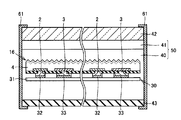
- FIG. 3 is a schematic cross-sectional view of the solar cell in the first embodiment.
- 6 is a schematic cross-sectional view of a modification of the solar cell of Embodiment 1.
- FIG. 6 is a schematic cross-sectional view of another modification of the solar cell in the first embodiment.
- FIG. 1 is typical sectional drawing of an example of the back electrode type photovoltaic cell used for the solar cell of Embodiment 2
- (b) is a part of light-receiving surface of the n-type silicon substrate shown to (a). It is a typical expanded sectional view of.
- (A)-(k) is typical sectional drawing illustrating about an example of the manufacturing method of the back surface electrode type photovoltaic cell used for the solar cell of Embodiment 2.
- FIG. In Embodiment 2 it is typical sectional drawing illustrating the process of sealing the back surface electrode type photovoltaic cell installed on the wiring sheet.
- 6 is a schematic cross-sectional view of a solar cell according to Embodiment 2.
- FIG. 6 is a schematic cross-sectional view of a modification of the solar cell of Embodiment 2.
- FIG. 6 is a schematic cross-sectional view of another modification of the solar cell of Embodiment 2.
- FIG. It is a typical block diagram illustrating a pseudo negative electrode ground test apparatus.
- FIG. 6 is a graph showing the relationship between the sheet resistance of the light-receiving surface diffusion layer of the back electrode type solar cells of Examples 1 to 8 and Comparative Examples 1 to 6 and the volume resistivity at 85 ° C. of the sealing material. It is a typical block diagram illustrating the process of sealing the solar cell array of the conventional solar cell module of patent document 1 with a sealing material.
- FIG. 1 the typical top view of the back surface of an example of the back electrode type solar cell used for the solar cell of Embodiment 1 is shown.
- the back electrode type solar cell 1 has a first conductivity type on the back surface which is the surface opposite to the light receiving surface side of the back electrode type solar cell 1 of the n-type silicon substrate 4 as the first conductivity type semiconductor substrate.
- the n-electrode 2 and the p-electrode 3 are alternately arranged on the back surface of the n-type silicon substrate 4. It is arranged.
- FIG. 2A shows a schematic cross-sectional view along II-II in FIG. 1, and FIG. 2B schematically shows a part of the light-receiving surface of the n-type silicon substrate 4 shown in FIG. 2A. An enlarged sectional view is shown. As shown in FIG. 2A, an uneven shape 5 is formed on the light receiving surface of the n-type silicon substrate 4.
- an n + layer 6 is formed as a light receiving surface diffusion layer which is an FSF layer.
- the n + layer 6 is a layer having the same n type conductivity type as the n type silicon substrate 4, and the n type impurity concentration of the n + layer 6 is higher than the n type impurity concentration of the n type silicon substrate 4. ing.
- a light-receiving surface passivation film 8 is formed on the n + layer 6.
- the light-receiving surface passivation film 8 is made of a silicon oxide film.
- the thickness of the light-receiving surface passivation film 8 is preferably 30 nm or more and 200 nm or less. When the thickness of the light-receiving surface passivation film 8 is 30 nm or more and 200 nm or less, the characteristics of the back electrode type solar cell 1 tend to be improved.
- an antireflection film 12 is formed on the light receiving surface passivation film 8.
- Antireflection film 12 includes an n-type impurity having the same n-type conductivity as n-type silicon substrate 4, and is made of, for example, a titanium oxide film containing phosphorus as an n-type impurity.
- the thickness of the antireflection film 12 can be, for example, 30 nm or more and 500 nm or less.
- phosphorus in the antireflection film 12 is contained as a phosphorus oxide in an amount of 15% by mass or more and 35% by mass or less of the antireflection film 7.
- 15 mass% or more and 35 mass% or less of the anti-reflective film 12 is contained as a phosphorus oxide that the content of the phosphorus oxide in the anti-reflective film 12 is 15 mass% or more and 35 mass% of the whole anti-reflective film 12. It means the following.
- an n ++ layer 10 which is an n-type impurity diffusion layer as a first conductivity-type impurity diffusion layer, and a second conductivity-type impurity diffusion layer are formed.
- P + layers 11 which are p-type impurity diffusion layers are alternately formed.
- a back surface passivation film 15 is formed on the back surface of the n type silicon substrate 4 by laminating a second back surface passivation film 14 and a first back surface passivation film 13 in this order from the n type silicon substrate 4 side.
- An n electrode 2 and a p electrode 3 are formed on the n ++ layer 10 and the p + layer 11 exposed from the back surface passivation film 15, respectively.
- the uneven shape 5 is formed on the light-receiving surface of the n-type silicon substrate 4 as shown in FIG. Form.
- a diffusion mask 22 is formed on the light receiving surface of the n-type silicon substrate 4, and a part of the back surface is formed.
- a diffusion mask 23 is formed, and then an n ++ layer 10 is formed on a part of the back surface of the n-type silicon substrate 4.
- the diffusion mask 24 is applied to the light-receiving surface of the n-type silicon substrate 4.
- a diffusion mask 25 is formed on a part of the back surface, and then a p + layer 11 is formed on a part of the back surface of the n-type silicon substrate 4.
- a solution 27 is applied to the light receiving surface of the n-type silicon substrate 4 and then dried.
- application and drying of the solution 27 can be performed, for example, as follows.
- a first back surface passivation film 13 that also serves as a diffusion mask such as a silicon oxide film having a thickness of 50 nm to 100 nm is formed on the back surface of the n-type silicon substrate 4.
- the first back surface passivation film 13 can be formed by, for example, CVD or SOG (spin-on-glass) coating and baking.
- a solution 27 containing a phosphorus-containing compound, titanium alkoxide, and alcohol is applied to the light-receiving surface of the n-type silicon substrate 4 by spin coating or the like and then dried.
- the compound containing phosphorus contained in the solution 27 for example, phosphorus pentoxide can be used.
- the titanium alkoxide for example, tetraisopropyl titanate can be used.
- alcohol isopropyl alcohol etc. can be used, for example.
- an n + layer 6, a light-receiving surface passivation film 8 and an antireflection film 12 are formed on the light-receiving surface of the n-type silicon substrate 4, and n
- a second back surface passivation film 14 is formed between the back surface of the mold silicon substrate 4 and the first back surface passivation film 13.
- the n + layer 6 and the antireflection film 12 can be formed by heat-treating the n-type silicon substrate 4 on which the solution 27 is applied to the light receiving surface, for example, at a temperature of 850 ° C. or more and 1000 ° C. or less. That is, by this heating, phosphorus diffuses from the solution 27 on the light receiving surface of the n-type silicon substrate 4 to form the n + layer 6 and the antireflection film 12 made of a titanium oxide film containing phosphorus.
- the light-receiving surface passivation film 8 and the second back surface passivation film 14 can be formed by performing thermal oxidation with oxygen or water vapor on the n-type silicon substrate 4 after the formation of the n + layer 6 and the antireflection film 12. it can. As a result, as shown in FIG. 3I, a light-receiving surface passivation film 8 is formed between the n + layer 6 on the light-receiving surface of the n-type silicon substrate 4 and the antireflection film 12, and an n-type silicon substrate is formed. 4, a second back surface passivation film 14 is formed between the back surface 4 and the first back surface passivation film 13.
- a laminated body of the first back surface passivation film 13 and the second back surface passivation film 14 is referred to as a back surface passivation film 15.
- the reason why the light-receiving surface passivation film 8 is formed between the n + layer 6 and the antireflection film 12 is that the film thickness of the antireflection film 12 in the concave portion of the concavo-convex shape 5 on the light receiving surface is increased and the antireflection film 12 is formed. It is considered that a silicon oxide film, which is the light-receiving surface passivation film 8, grows due to oxygen or water vapor entering from the portion where the crack is generated.
- the antireflection film 12 is thin at the convex portion of the concave-convex shape 5 on the light receiving surface, it is considered that oxygen or water vapor is transmitted and a silicon oxide film that is the light receiving surface passivation film 8 grows. Furthermore, the reason why the second back surface passivation film 14 is formed between the back surface of the n-type silicon substrate 4 and the first back surface passivation film 13 is that the first back surface passivation film on the back surface of the n-type silicon substrate 4 is used. Since 13 is a film formed by a CVD method or the like, it is considered that oxygen or water vapor passes through the inside of the first back surface passivation film 13, thereby growing a silicon oxide film as the second back surface passivation film 14. .
- the thickness of the light-receiving surface passivation film 8 is not less than 100 nm and not more than 200 nm, for example, and the thickness of the second back surface passivation film 14 is not less than 30 nm and not more than 100 nm on the n ++ layer 10, for example. On the layer 11, the thickness is 10 nm or more and 40 nm or less.
- the thermal oxidation of the n-type silicon substrate 4 with oxygen or water vapor for forming the light-receiving surface passivation film 8 and the second back surface passivation film 14 is performed by placing the n-type silicon substrate 4 in an oxygen atmosphere or a water vapor atmosphere. It can carry out by heat-processing in a state.
- the sheet resistance of the n + layer 6 is 40 ⁇ / ⁇ or more and 80 ⁇ / ⁇ or less. Note that the sheet resistance of the n + layer 6 can be appropriately adjusted by changing at least one of the phosphorus content in the solution 27, the temperature during the thermal oxidation, and the time, for example.
- the light-receiving surface passivation film 8 and the second back surface passivation film 14 are n-type silicon substrates by switching the atmosphere gas to an oxygen atmosphere or a water vapor atmosphere following the heat treatment for forming the n + layer 6 and the antireflection film 12. 4 can also be formed by performing thermal oxidation.
- a part of the back surface passivation film 15 is removed to expose a part of the n ++ layer 10 and a part of the p + layer 11 from the back surface passivation film 9. .
- the n electrode 2 is formed on the n + + layer 10 and the p electrode 3 is formed on the p + layer 11.
- the back electrode type solar cell 1 can be manufactured.
- the wiring sheet 30 includes an insulating substrate 31 and wirings 36 installed on the surface of the insulating substrate 31.
- the wiring 36 includes an n wiring 32, an n wiring 32 a, a p wiring 33, a p wiring 33 a, and a connection wiring 34.
- the n wiring 32, the n wiring 32a, the p wiring 33, the p wiring 33a, and the connection wiring 34 are conductive.
- the n wiring 32 and the p wiring 33 have a comb shape including a shape in which a plurality of rectangles are arranged in a direction orthogonal to the longitudinal direction of the rectangle.
- the n wiring 32a, the p wiring 33a, and the connection wiring 34 are strip-shaped.
- the adjacent n wiring 32 and the p wiring 33 other than the n wiring 32 a and the p wiring 33 a located at the end of the wiring sheet 30 are electrically connected by the connection wiring 34.
- the portions corresponding to the comb teeth (rectangular) of the comb-shaped n wiring 32 and the portions corresponding to the comb teeth (rectangular) of the comb-shaped p wiring 33 are alternately meshed one by one.
- the n wiring 32 and the p wiring 33 are arranged.
- a portion corresponding to the comb teeth of the comb-shaped n wiring 32 and a portion corresponding to the comb teeth of the comb-shaped p wiring 33 are alternately arranged at predetermined intervals. .
- at least one of the portions corresponding to the comb teeth of the n wiring 32 and the p wiring 33 may be alternately arranged instead of one.
- the insulating base material 31 can be used without particular limitation as long as it is an electrically insulating material.
- PET polyethylene terephthalate
- PEN polyethylene naphthalate
- PET polyphenylene sulfide
- a material containing at least one resin selected from the group consisting of PPS (Polyphenylene sulfide), polyvinyl fluoride (PVF) and polyimide (Polyimide) can be used.
- the thickness of the insulating substrate 31 is not particularly limited, and can be, for example, 25 ⁇ m or more and 150 ⁇ m or less.
- the insulating base 31 may have a single-layer structure consisting of only one layer or a multi-layer structure consisting of two or more layers.
- the material of the wiring 36 can be used without particular limitation as long as it is a conductive material.
- a conductive material For example, at least one selected from the group consisting of copper (Cu), aluminum (Al), and silver (Ag) is used.
- a metal containing, for example, can be used.
- the thickness of the wiring 36 is not particularly limited, and can be, for example, 10 ⁇ m or more and 50 ⁇ m or less.
- the shape of the wiring 36 is not limited to the shape described above, and can be set as appropriate.
- At least a part of the surface of the wiring 36 has, for example, nickel (Ni), gold (Au), platinum (Pt), palladium (Pd), silver (Ag), tin (Sn), SnPb solder, and ITO (Indium).
- a conductive substance containing at least one selected from the group consisting of Tin Oxide may be installed. In this case, there is a tendency that the electrical connection between the wiring 36 of the wiring sheet 30 and the electrode of the back electrode type solar battery cell to be described later can be improved, and the weather resistance of the wiring 36 can be improved.
- At least a part of the surface of the wiring 36 may be subjected to a surface treatment such as a rust prevention treatment or a blackening treatment.
- the wiring 36 may also have a single-layer structure consisting of only one layer, or a multi-layer structure consisting of two or more layers.
- an insulating substrate 31 such as a PET film is prepared, and a conductive material such as a metal foil or a metal plate is bonded to the entire surface of one surface of the insulating substrate 31.
- a conductive material such as a metal foil or a metal plate is bonded to the entire surface of one surface of the insulating substrate 31.
- a roll of an insulating base material cut to a predetermined width is pulled out, an adhesive is applied to one surface of the insulating base material 31, and a roll of metal foil cut slightly smaller than the width of the insulating base material 31 is applied.
- a wiring 36 including an n wiring 32, an n wiring 32a, a p wiring 33, a p wiring 33a, and a connection wiring 34 made of a conductive material is formed.
- the wiring sheet 30 having the configuration shown in FIG. 4 can be manufactured.
- FIG. 5 is a schematic plan view illustrating a state where the back electrode type solar cell 1 is installed on the wiring sheet 30 shown in FIG.
- the back electrode type solar cell 1 is installed on the wiring sheet 30 such that the back side of the back electrode type solar cell 1 faces the installation side of the wiring 36 of the wiring sheet 30.
- the back electrode type solar cell 1 is arranged on the wiring sheet 30 so that the n electrode 2 and the p electrode 3 of the back electrode type solar cell 1 are in contact with the n wiring 32 and the p wiring 33 of the wiring sheet 30, respectively.
- the n electrode 2 and the p electrode 3 may be mechanically and electrically connected to the n wiring 32 and the p wiring 33 by a conductive adhesive such as solder, for example.
- the n electrode 2 and the p electrode 3 are respectively connected to the n wiring 32 and the p electrode 3 by the shrinkage force when the insulating resin composition placed between the back electrode type solar cell 1 and the wiring sheet 30 is cured.
- the wiring 33 may be directly connected to be electrically connected and mechanically connected.
- the back electrode type solar cells installed so as to be adjacent to each other on the wiring sheet 30.
- the ones are electrically connected to each other.
- all the back surface electrode type photovoltaic cells 1 installed on the wiring sheet 30 are electrically connected in series.
- FIG. 6 is a schematic cross-sectional view illustrating the process of sealing the back electrode type solar battery cell 1 installed on the wiring sheet 30.
- the sheet-like first resin layer 40, the sheet-like second resin layer 41, and the transparent protective substrate. 42 are arranged in this order.
- the sheet-like first resin layer 40 and the back surface protection sheet 43 are arranged in this order from the wiring sheet 30 side.
- any substrate that is transparent to sunlight can be used without particular limitation, and for example, a glass substrate or the like can be used.
- the first resin layer 40 was selected from the group consisting of ethylene vinyl acetate resin, epoxy resin, acrylic resin, urethane resin, olefin resin, polyester resin, silicone resin, polystyrene resin, polycarbonate resin, and rubber resin, for example.
- a layer made of at least one transparent resin can be used.
- the second resin layer 41 a layer made of an olefin resin is preferably used.
- the olefin resin used for the second resin layer 41 for example, at least one selected from the group consisting of a polyethylene resin, a polypropylene resin, and a polybutene resin can be used.
- the polyethylene-based resin is an ethylene homopolymer or a copolymer of ethylene and one or more other monomers.
- the polypropylene resin is a homopolymer of propylene or a copolymer of propylene and one or more other monomers.
- the polybutene resin is a butene homopolymer or a copolymer of butene and one or more other monomers.
- polyethylene resin for example, polyethylene or ethylene- ⁇ -olefin copolymer can be used.
- polyethylene examples include low density polyethylene, linear low density polyethylene, and linear ultra-low density polyethylene.
- ethylene- ⁇ -olefin copolymer a copolymer comprising ethylene and at least one selected from ⁇ -olefins having 3 to 20 carbon atoms is preferably used, and ethylene and carbon atoms having 3 to 12 carbon atoms are used. It is more preferable to use a copolymer comprising at least one selected from ⁇ -olefins.
- the ⁇ -olefin include propylene, 1-butene, 1-pentene, 1-hexene, 1-octene, 4-methyl-1-pentene, 3-methyl-1-pentene, 1-decene and 1-dodecene. , 1-tetradecene, 1-hexadecene, 1-octadecene, and 1-eicosane can be used.
- polypropylene resin for example, a propylene- ⁇ -olefin copolymer or a terpolymer of propylene, ethylene, and ⁇ -olefin can be used.
- the propylene- ⁇ -olefin copolymer is a copolymer composed of at least one selected from propylene and ⁇ -olefin.
- a copolymer comprising at least one selected from ethylene and an ⁇ -olefin having 3 to 20 carbon atoms and propylene is preferably used, and ethylene and 4 to 4 carbon atoms are preferably used. It is more preferable to use a copolymer comprising at least one selected from 8 ⁇ -olefins and propylene.
- Examples of the ⁇ -olefin having 3 to 20 carbon atoms include propylene, 1-butene, 1-pentene, 1-hexene, 1-octene, 4-methyl-1-pentene, 3-methyl-1-pentene, 1 At least one selected from the group consisting of -decene, 1-dodecene, 1-tetradecene, 1-hexadecene, 1-octadecene and 1-eicosane can be used.
- polybutene resin for example, a crystalline copolymer comprising at least one selected from ethylene, propylene, and an olefin compound having 5 to 8 carbon atoms and butene can be used.
- the first resin layer 40 and the second resin layer 41 may contain conventionally known additives such as a crosslinking agent in addition to the above resin components. Further, the first resin layer 40 and the second resin layer 41 are formed into a sheet shape by, for example, mixing a conventionally known additive such as a crosslinking agent into the above resin component and molding the mixture into a predetermined shape. can do.
- a conventionally known additive such as a crosslinking agent
- any material can be used without particular limitation as long as it can protect the back surface of the first resin layer 40.
- a weathering film such as PET that has been conventionally used may be used. it can.
- the back surface protection sheet 43 includes a metal film such as aluminum, for example. Also good.
- the back surface protection sheet 43 such as the end face of the solar cell module with a moisture permeation preventing tape such as a butyl rubber tape.
- the back electrode type solar cell 1 sealed in the sealing material 50 is not limited to plural, and may be single.
- the sheet resistance of the n + layer 6 as the light-receiving surface diffusion layer of the back electrode type solar cell 1 is set to 40 ⁇ / ⁇ or more and 80 ⁇ / ⁇ or less, and the back electrode type solar cell 1
- the volume resistivity at 85 ° C. of the sealing material (second resin layer 41) provided on the light receiving surface is set to 1 ⁇ 10 16 ⁇ ⁇ cm or less.
- the sheet resistance of the n + layer 6 as the light-receiving surface diffusion layer is set to 40 ⁇ / ⁇ or more and 80 ⁇ / ⁇ or less, so that the light-receiving surface of the back electrode type solar cell 1 is obtained.
- the sheet resistance of the n + layer 6 as the light-receiving surface diffusion layer of the back electrode type solar cell 1 is less than 40 ⁇ / ⁇ , recombination in the n + layer 6 increases, so that the back electrode type The output of the solar battery cell 1 itself decreases.
- the sheet resistance of the n + layer 6 is higher than 80 ⁇ / ⁇ , a large potential difference is generated between the back electrode type solar cell 1 and the frame 61, and moisture or the like is present on the surface of the transparent protective substrate 42. If accumulated, charge accumulates in the light-receiving surface passivation film 8 of the back electrode type solar cell 1, and the function of the n + layer 6 as an FSF (Front Surface Field) deteriorates.
- FSF Front Surface Field
- the volume resistivity at 45 ° C. to 85 ° C. is as high as 1 ⁇ 10 16 ⁇ ⁇ cm or higher. Since it is possible to suppress a decrease in output due to PID or the like without using a special sealing material, the choice of sealing material provided on the light-receiving surface of the back electrode type solar cell 1 is more than conventional. It can be expanded and long-term reliability can be ensured.
- a high-resistance special resistance having a volume resistivity of 1 ⁇ 10 16 ⁇ ⁇ cm or more at 45 ° C. to 85 ° C.
- the manufacturing cost of the solar cell module can be kept low.
- the volume resistivity at 45 ° C. to 85 ° C. is as high as 1 ⁇ 10 16 ⁇ ⁇ cm or more, Since it is not necessary to use a sealing material that is very difficult to handle, the manufacturing efficiency of the solar cell module can be improved.
- the volume resistivity at 85 ° C. of the sealing material (second resin layer 41) provided on the light receiving surface of the back electrode type solar cell 1 is 1 ⁇ 10 12 ⁇ ⁇ cm or more and 1 ⁇ 10 16 ⁇ ⁇ cm or less, 1 ⁇ 10 15 ⁇ ⁇ 1 ⁇ more preferably not more than 10 16 Omega ⁇ cm or more cm, 2.8 ⁇ 10 15 ⁇ ⁇ cm or more 5.1 ⁇ 10 15 ⁇ ⁇ cm More preferably, it is as follows. In these cases, the long-term reliability of the solar cell of Embodiment 1 can be further improved without using a special and expensive sealing material.
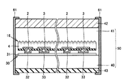
- FIG. 8 shows a schematic cross-sectional view of a modification of the solar cell of the first embodiment.
- the sealing material 50 that seals the back electrode type solar cell 1 is the second resin on the light receiving surface of the back electrode type solar cell 1. It consists of the laminated body of the layer 41 and the 1st resin layer 40 on the wiring sheet 30, It is characterized by the above-mentioned.
- the sheet resistance of n + layer 6 as the light-receiving surface diffusion layer of back electrode type solar cell 1 is set to 40 ⁇ / ⁇ or more and 80 ⁇ / ⁇ or less. Therefore, a sealing material having a volume resistivity of 1 ⁇ 10 16 ⁇ ⁇ cm or less at 85 ° C. is used as the sealing material (second resin layer 41) provided on the light receiving surface of the back electrode type solar cell 1. be able to. Thereby, the modification of the solar cell of Embodiment 1 shown in FIG. 8 can also be set as the solar cell which can ensure long-term reliability, without using a special and expensive sealing material.
- FIG. 9 shows a schematic cross-sectional view of another modification of the solar cell of the first embodiment.
- the sealing material for sealing the back electrode type solar cell 1 is composed of a sealing material 52 made of a single layer of olefin resin. It is characterized by that.
- the sheet resistance of the n + layer 6 as the light-receiving surface diffusion layer of the back electrode type solar cell 1 is 40 ⁇ / ⁇ or more and 80 ⁇ / ⁇ or less. Therefore, as the sealing material provided on the light receiving surface of the back electrode type solar cell 1, the sealing material 52 made of a single layer of olefin resin having a volume resistivity at 85 ° C. of 1 ⁇ 10 16 ⁇ ⁇ cm or less. Can be used. Thereby, the other modification of the solar cell of Embodiment 1 shown in FIG. 9 can also be made into a solar cell which can ensure long-term reliability, without using a special and expensive sealing material.
- the first conductivity type is n-type and the second conductivity type is p-type.
- the present invention is not limited to this, and the first conductivity type is p-type.
- the second conductivity type may be n-type.
- the n-type silicon substrate is a p-type silicon substrate
- the light-receiving surface diffusion layer is a p + layer in which p-type impurities are diffused.
- the antireflection film is made of a titanium oxide film containing p-type impurities.
- the concept of the back electrode type solar cell which is one embodiment of the present invention includes a back electrode type solar cell having a configuration in which both an n electrode and a p electrode are formed only on one surface (back surface) of a semiconductor substrate.
- a solar cell having a configuration such as an MWT (Metal Wrap Through) type (a solar cell in which a part of an electrode is disposed in a through hole provided in a semiconductor substrate) is also included.
- MWT Metal Wrap Through
- FIG. 10 (a) shows a schematic cross-sectional view of an example of a back electrode type solar battery cell used in the solar battery of Embodiment 2
- FIG. 10 (b) shows an n-type silicon substrate shown in FIG. 10 (a).
- 4 is a schematic enlarged cross-sectional view of a part of the light receiving surface 4. As shown in FIG. 10A, an uneven shape 5 is formed on the light receiving surface of the n-type silicon substrate 4.
- an n + layer 6 is formed as a light receiving surface diffusion layer which is an FSF layer.
- the n + layer 6 is a layer having the same n type conductivity type as the n type silicon substrate 4, and the n type impurity concentration of the n + layer 6 is higher than the n type impurity concentration of the n type silicon substrate 4. ing.
- a light-receiving surface passivation film 8 is formed on the n + layer 6.
- the light-receiving surface passivation film 8 is made of a silicon oxide film.
- the thickness of the light-receiving surface passivation film 8 is preferably 30 nm or more and 200 nm or less. When the thickness of the light-receiving surface passivation film 8 is 30 nm or more and 200 nm or less, the characteristics of the back electrode type solar battery cell 16 tend to be improved.
- an antireflection film 7 is formed on the light receiving surface passivation film 8.
- the antireflection film 7 includes an n-type impurity having the same n-type conductivity as that of the n-type silicon substrate 4 and is made of, for example, a titanium oxide film containing phosphorus as an n-type impurity.
- the thickness of the antireflection film 7 can be set to, for example, 0 nm or more and 500 nm or less.
- the location where the thickness of the antireflection film 7 is 0 nm means that the portion of the antireflection film 7 is not formed.
- phosphorus in the antireflection film 7 is contained as a phosphorus oxide in an amount of 15% by mass to 35% by mass of the antireflection film 7.
- 15 mass% or more and 35 mass% or less of the anti-reflective film 7 are contained as phosphorous oxide, when the content of phosphorus oxide in the anti-reflective film 7 is 15 mass% or more and 35 mass% of the whole anti-reflective film 7. It means the following.
- an n ++ layer 10 which is an n-type impurity diffusion layer as a first conductivity-type impurity diffusion layer, and a second conductivity-type impurity diffusion layer are formed.
- P + layers 11 which are p-type impurity diffusion layers are alternately formed.
- a back surface passivation film 9 made of a silicon oxide film is formed on a part of the back surface of the n-type silicon substrate 4.
- An n electrode 2 and a p electrode 3 are formed on the n ++ layer 10 and the p + layer 11 exposed from the back surface passivation film 9, respectively.
- a texture mask 21 is formed on the back surface of the n-type silicon substrate 4.
- a texture mask 21 for example, a silicon nitride film or the like can be used.
- the texture mask 21 can be formed by, for example, a CVD (Chemical Vapor Deposition) method or a sputtering method.
- an uneven shape 5 is formed on the light receiving surface of the n-type silicon substrate 4.
- the uneven shape 5 can have a texture structure, for example.
- the uneven shape 5 is formed by etching the light-receiving surface of the n-type silicon substrate 4 with a solution in which isopropyl alcohol is added to an alkaline aqueous solution such as a sodium hydroxide aqueous solution or a potassium hydroxide aqueous solution and heated to 70 ° C. or higher and 80 ° C. or lower. Can be formed.
- an n ++ layer 10 is formed on a part of the back surface of the n-type silicon substrate 4.
- the n ++ layer 10 can be formed as follows, for example.
- the texture mask 21 on the back surface of the n-type silicon substrate 4 is removed.
- a diffusion mask 22 such as a silicon oxide film is formed on the light receiving surface of the n-type silicon substrate 4.
- a diffusion mask 23 is formed by applying a masking paste to a region other than the region where the n ++ layer 10 is formed on the back surface of the n-type silicon substrate 4 and then heat-treating the masking paste.
- the n ++ layer 10 is formed by diffusing phosphorus from the diffusion mask 23 to the portion where the back surface of the n-type silicon substrate 4 is exposed by vapor phase diffusion using POCl 3 .
- the thing containing a solvent, a thickener, and a silicon oxide precursor etc. can be used, for example.
- a method for applying the masking paste for example, an ink jet printing method or a screen printing method can be used.
- a p + layer 11 is formed on a part of the back surface of the n-type silicon substrate 4.
- the p + layer 11 can be formed, for example, as follows.
- a diffusion mask 24 such as a silicon oxide film is formed on the light receiving surface of the n-type silicon substrate 4.
- a diffusion mask 25 is formed by applying a masking paste to a region other than the region where the p + layer 11 is formed on the back surface of the n-type silicon substrate 4 and then heat-treating the masking paste.
- a solution obtained by dissolving a polymer obtained by reacting a boron compound with an organic polymer in an alcohol aqueous solution is applied to the back surface of the n-type silicon substrate 4, dried, and then subjected to heat treatment.
- a p + layer 11 is formed by diffusing boron in the portion where the back surface of the mold silicon substrate 4 is exposed.
- the solution 27 is applied to the light receiving surface of the n-type silicon substrate 4 and then dried.
- application and drying of the solution 27 can be performed, for example, as follows.
- a diffusion mask 26 such as a silicon oxide film is formed on the back surface of the n-type silicon substrate 4.
- a solution 27 containing, for example, a compound containing phosphorus as a compound containing impurities of the first conductivity type, titanium alkoxide, and alcohol is applied to the light receiving surface of the n-type silicon substrate 4 by a spin coating method or the like. Later dry.
- phosphorus pentoxide can be used as the compound containing phosphorus contained in the solution 27.
- titanium alkoxide for example, tetraisopropyl titanate can be used.
- alcohol isopropyl alcohol etc. can be used, for example.
- an n + layer 6 and an antireflection film 7 are formed on the light receiving surface of the n-type silicon substrate 4.
- the n + layer 6 and the antireflection film 7 can be formed by heat-treating the n-type silicon substrate 4 on which the solution 27 is applied to the light receiving surface, for example, at a temperature of 850 ° C. or more and 1000 ° C. or less. That is, by this heating, phosphorus is diffused from the solution 27 on the light receiving surface of the n-type silicon substrate 4 to form the n + layer 6 and the antireflection film 7 made of a titanium oxide film containing phosphorus is formed.
- a light-receiving surface passivation film 8 is formed on the light-receiving surface of the n-type silicon substrate 4.
- the light-receiving surface passivation film 8 can be formed, for example, as follows.
- the diffusion mask 26 on the back surface of the n-type silicon substrate 4 is removed by etching using hydrofluoric acid.
- a part of the antireflection film 7 is also etched by hydrofluoric acid, and a part of the light receiving surface of the n-type silicon substrate 4 is exposed.
- the antireflection film 7 is made of a titanium oxide film containing phosphorus, it has high hydrofluoric acid resistance. As a result, as shown in FIG. 11 (k), only the convex portions of the concave-convex shape 5 on the light receiving surface of the n-type silicon substrate 4 where the antireflection film 7 is thin are exposed.
- n-type silicon substrate 4 thermal oxidation of the n-type silicon substrate 4 with oxygen or water vapor is performed.
- a back surface passivation film 9 made of a silicon oxide film is formed on the back surface of the n-type silicon substrate 4, and a light receiving surface passivation film 8 made of a silicon oxide film is also formed on the light receiving surface of the n type silicon substrate 4.
- the n + layer 6 and the antireflection film 7 on the light-receiving surface of the n-type silicon substrate 4 together with the convex portions of the uneven shape 5 on the light-receiving surface from which the n-type silicon substrate 4 is exposed.
- the light-receiving surface passivation film 8 is also formed between the two.
- the reason why the light-receiving surface passivation film 8 is formed between the n + layer 6 and the antireflection film 7 is that the film thickness of the antireflection film 7 in the concave portion of the concavo-convex shape 5 on the light receiving surface is increased and the antireflection film 7 is formed. It is considered that a silicon oxide film, which is the light-receiving surface passivation film 8, grows due to oxygen or water vapor entering from the portion where the crack is generated.
- the thickness of the light-receiving surface passivation film 8 is, for example, 100 nm or more and 200 nm or less, and the thickness of the back surface passivation film 9 is, for example, 30 nm or more and 100 nm or less on the n ++ layer 10, and on the p + layer 11. Is 10 nm or less.
- the thermal oxidation of the n-type silicon substrate 4 with oxygen or water vapor can be performed by heat treatment in a state where the n-type silicon substrate 4 is placed in an oxygen atmosphere or a water vapor atmosphere.
- the sheet resistance of the n + layer 6 is 40 ⁇ / ⁇ or more and 80 ⁇ / ⁇ or less. Note that the sheet resistance of the n + layer 6 can be appropriately adjusted by changing at least one of the phosphorus content in the solution 27, the temperature during the thermal oxidation, and the time, for example.
- a part of the back surface passivation film 9 is removed to expose a part of the n ++ layer 10 and a part of the p + layer 11 from the back surface passivation film 9, respectively.
- a part of the back surface passivation film 9 can be removed, for example, by applying the etching paste to a part of the back surface passivation film 9 by a screen printing method or the like and then heating the etching paste. Thereafter, the etching paste can be removed, for example, by performing an acid treatment after ultrasonic cleaning.
- the etching paste includes, for example, at least one selected from the group consisting of phosphoric acid, hydrogen fluoride, ammonium fluoride, and ammonium hydrogen fluoride as an etching component, and also includes water, an organic solvent, and a thickener. Things can be used.
- the n electrode 2 is formed on the n + + layer 10 and the p electrode 3 is formed on the p + layer 11.
- the n electrode 2 and the p electrode 3 are dried by applying a silver paste to a predetermined position of the back surface passivation film 9 on the back surface of the n-type silicon substrate 4 by screen printing, and then firing the silver paste. Can be formed.
- the back surface electrode type solar cell 16 used for the solar cell of Embodiment 2 can be manufactured.
- FIG. 12 is a schematic cross-sectional view illustrating the process of sealing the back electrode type solar cells 16 installed on the wiring sheet 30.
- the sheet-like first resin layer 40, the sheet-like second resin layer 41, and the transparent protective substrate 42 are arranged in this order.
- the sheet-like first resin layer 40 and the back surface protection sheet 43 are arranged in this order from the wiring sheet 30 side.
- the back surface electrode type solar cell 16 sealed in the sealing material 50 is not limited to plural, and may be single.
- the sheet resistance of the n + layer 6 as the light-receiving surface diffusion layer of the back electrode type solar cell 16 is set to 40 ⁇ / ⁇ or more and 80 ⁇ / ⁇ or less, and the back electrode type solar cell 16
- the volume resistivity at 85 ° C. of the sealing material (second resin layer 41) provided on the light receiving surface is set to 1 ⁇ 10 16 ⁇ ⁇ cm or less.
- the sheet resistance of the n + layer 6 as the light-receiving surface diffusion layer of the back electrode type solar cell 16 is less than 40 ⁇ / ⁇ , recombination in the n + layer 6 increases, so that the back electrode type The output of the solar battery cell 16 itself decreases.
- the sheet resistance of the n + layer 6 is higher than 80 ⁇ / ⁇ , a large potential difference is generated between the back electrode type solar cell 16 and the frame 61, and moisture or the like is present on the surface of the transparent protective substrate 42. If accumulated, charge accumulates in the light-receiving surface passivation film 8 of the back electrode type solar cell 16, and the function of the n + layer 6 as an FSF (Front Surface Field) deteriorates.
- FSF Front Surface Field
- the volume resistivity at 45 ° C. to 85 ° C. is as high as 1 ⁇ 10 16 ⁇ ⁇ cm or more. Since it is possible to suppress a decrease in output due to PID or the like without using a special sealing material, the choice of the sealing material provided on the light-receiving surface of the back electrode type solar cell 16 as compared with the prior art It can be expanded and long-term reliability can be ensured.
- a special high resistance material having a volume resistivity of 1 ⁇ 10 16 ⁇ ⁇ cm or more at 45 ° C. to 85 ° C.
- the manufacturing cost of the solar cell module can be kept low.
- the volume resistivity at 45 ° C. to 85 ° C. is as high as 1 ⁇ 10 16 ⁇ ⁇ cm or more, Since it is not necessary to use a sealing material that is very difficult to handle, the manufacturing efficiency of the solar cell module can be improved.
- FIG. 14 shows a schematic cross-sectional view of a modification of the solar cell of the second embodiment.
- the sealing material 50 that seals the back electrode type solar cell 16 is the second resin on the light receiving surface of the back electrode type solar cell 16. It consists of the laminated body of the layer 41 and the 1st resin layer 40 on the wiring sheet 30, It is characterized by the above-mentioned.
- the sheet resistance of n + layer 6 as the light-receiving surface diffusion layer of back electrode type solar cell 16 is set to 40 ⁇ / ⁇ or more and 80 ⁇ / ⁇ or less. Therefore, a sealing material (second resin layer 41) having a volume resistivity of 1 ⁇ 10 16 ⁇ ⁇ cm or less at 85 ° C. is used as the sealing material provided on the light receiving surface of the back electrode type solar cell 16. be able to.
- the modification of the solar cell of Embodiment 2 shown in FIG. 14 can also be made into a solar cell which can ensure long-term reliability, without using a special and expensive sealing material.
- FIG. 15 is a schematic cross-sectional view of another modification of the solar cell of the second embodiment.
- the sealing material for sealing back electrode type solar battery cell 16 is formed of sealing material 52 made of a single layer of olefin resin. It is characterized by that.
- the sheet resistance of the n + layer 6 as the light-receiving surface diffusion layer of the back electrode type solar cell 16 is 40 ⁇ / ⁇ or more and 80 ⁇ / ⁇ or less. Therefore, as a sealing material provided on the light receiving surface of the back electrode type solar cell 16, a sealing material 52 made of a single layer of an olefin resin having a volume resistivity at 85 ° C. of 1 ⁇ 10 16 ⁇ ⁇ cm or less. Can be used. Thereby, the other modification of the solar cell of Embodiment 1 shown in FIG. 15 can also be set as the solar cell which can ensure long-term reliability, without using a special and expensive sealing material.
- the back electrodes of Examples 1 to 5 and Comparative Examples 1 to 3 were manufactured by the same method as that for manufacturing the back electrode type solar battery cell of Embodiment 1 shown in FIGS. 3 (a) to 3 (i).
- Type solar cell 1 was produced.
- the back electrodes of Examples 6 to 8 and Comparative Examples 4 to 6 were produced by the same method as the method of manufacturing the back electrode type solar cell of Embodiment 2 shown in FIGS. 11 (a) to 11 (k).
- Type solar cell 16 was produced.
- the back electrode type solar cells 1 of Examples 1 to 5 and Comparative Examples 1 to 3 are composed of phosphorus pentoxide, tetraisopropyl titanate, and isopropyl alcohol used for forming the n + layer 6 that is the light receiving surface diffusion layer. As shown in Table 1, by adjusting the phosphorous concentration in the solution 27 containing N, the sheet resistance of the n + layer 6 was changed, and the same conditions and the same method were used.
- the back electrode type solar cells 16 of Examples 6 to 8 and Comparative Examples 4 to 6 also contain phosphorus pentoxide, tetraisopropyl titanate, and isopropyl alcohol used for forming the n + layer 6 that is the light receiving surface diffusion layer. As shown in Table 1, by adjusting the phosphorous concentration in the solution 27 to be contained, it was produced under the same conditions and the same method except that the sheet resistance of the n + layer 6 was changed.
- the sheet resistance values of the light-receiving surface diffusion layers of the back electrode type solar cells of Examples 1 to 8 and Comparative Examples 1 to 6 shown in Table 1 were determined using Examples 1 to 8 and Mirror wafer.
- the sample was formed up to the n + layer 6 under the same conditions and in the same manner as the back electrode type solar cells of Comparative Examples 1 to 6, and then the sample with the surface of the n + layer 6 exposed was prepared.
- the value measured by the four-probe method at room temperature (25 ° C.) was used.
- the back electrode type solar cells 1 of Examples 1 to 8 and Comparative Examples 1 to 6 were respectively installed on the wiring sheet 30, and a transparent protective substrate 42 made of glass,
- the volume resistivity at 85 ° C. was adjusted to be different as shown in Table 1 by changing the content of the additive between the back protective sheet 43 made of a PET film on which an aluminum film was deposited. It sealed in the sealing material 52 which consists of a single layer of an olefin resin.
- the volume resistivity values at 85 ° C. of the sealing materials used for sealing the back electrode type solar cells of Examples 1 to 8 and Comparative Examples 1 to 6 shown in Table 1 are as follows. Asked.
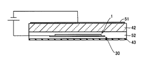
- a copper foil having a diameter of 5 cm On a Teflon (registered trademark) sheet, a copper foil having a diameter of 5 cm, a sealing material having a length of about 10 cm ⁇ width of about 10 cm ⁇ thickness of about 0.04 cm, a copper foil having a diameter of 5 cm, and a Teflon (registered trademark) sheet
- the encapsulating material was cured by applying the pressure under the same conditions as when the back electrode type solar cells were sealed, and then heating.
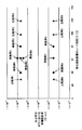
- FIG. 17 shows the relationship between the sheet resistance of the light-receiving surface diffusion layer of the back electrode type solar cells of Examples 1 to 8 and Comparative Examples 1 to 6 and the volume resistivity at 85 ° C. of the sealing material.
- the pseudo negative electrode 51 is grounded, and the back electrode type solar cell in an environment of 85 ° C.
- a pseudo negative electrode ground test was performed in which a voltage of 600 V was applied between 1 and the pseudo negative electrode 51 and left for 20 hours.
- Cell output change rate [%] 100 ⁇ ⁇ (cell output after pseudo negative grounding test) ⁇ (cell output before pseudo negative grounding test) ⁇ / (cell output before pseudo negative grounding test) (I)
- the sheet resistance of the light-receiving surface diffusion layer shown in Table 1 the volume resistivity of the sealing material at 85 ° C., the cell output before and after the pseudo negative electrode grounding test, and the output change rate are average values of n number of 5, respectively. is there.
- the sheet resistance of the light-receiving surface diffusion layer is 40 ⁇ / ⁇ or more and 80 ⁇ / ⁇ or less, and the volume resistivity at 85 ° C. of the sealing material is 1 ⁇ 10 16 ⁇ ⁇ cm or less All of the solar cells of ⁇ 8 were evaluated as A, and the solar cells of Comparative Examples 1-6 were all evaluated as B.
- the solar cells of Examples 1 to 8 can make the output of the back electrode type solar cell 1 itself higher than the solar cells of Comparative Examples 1 to 6, and the back electrode type solar cell. It was confirmed that a decrease in the output of the solar cell including 1 can be stably and sufficiently suppressed.
- the solar cells of Examples 1 to 5 in which the volume resistivity at 85 ° C. of the encapsulant is 2.8 ⁇ 10 15 ⁇ ⁇ cm or more and 5.1 ⁇ 10 15 ⁇ ⁇ cm or less the back electrode type solar cell It was confirmed that the decrease in the output of the solar battery including the battery cell 1 can be more stably and sufficiently suppressed.
- the solar cells of Examples 1 to 8 can ensure long-term reliability without using a special and expensive sealing material.
- the present invention comprises a back electrode type solar cell and a sealing material provided on the light receiving surface of the back electrode type solar cell, the back electrode type solar cell comprising a first conductivity type semiconductor substrate, A first conductive type light receiving surface diffusion layer provided on the light receiving surface side surface of the semiconductor substrate, and a first conductive type impurity diffusion layer and a second conductive type provided on the surface opposite to the light receiving surface side of the semiconductor substrate.
- the sheet resistance of the light-receiving surface diffusion layer is 40 ⁇ / ⁇ or more and 80 ⁇ / ⁇ or less, and the volume resistivity at 85 ° C. of the sealing material is 1 ⁇ 10 16 ⁇ ⁇ cm or less. It is a solar cell. With such a configuration, long-term reliability of the solar cell can be ensured without using a special and expensive sealing material.
- the light-receiving surface diffusion layer may be formed by applying a heat treatment after applying a solution containing a compound containing a first conductivity type impurity, titanium alkoxide, and alcohol. preferable. With such a configuration, the long-term reliability of the solar cell can be ensured without using a special and expensive sealing material.
- the sealing material is preferably composed of a single layer of olefin resin. Even if it is set as such a structure, long-term reliability of a solar cell can be ensured, without using a special and expensive sealing material.
- the sealing material includes a first resin layer on the light receiving surface of the back electrode type solar cell and a second resin layer on the first resin layer, and the second resin layer.
- the resin layer is preferably made of an olefin resin. Even if it is set as such a structure, long-term reliability of a solar cell can be ensured, without using a special and expensive sealing material.
- the volume resistivity of the encapsulant at 85 ° C. is preferably 1 ⁇ 10 12 ⁇ ⁇ cm or more and 1 ⁇ 10 16 ⁇ ⁇ cm or less.
- the volume resistivity of the sealing material is preferably 1 ⁇ 10 15 ⁇ ⁇ cm or more and 1 ⁇ 10 16 ⁇ ⁇ cm or less.
- the volume resistivity of the sealing material is preferably 2.8 ⁇ 10 15 ⁇ ⁇ cm or more and 5.1 ⁇ 10 15 ⁇ ⁇ cm or less.
- the present invention is a method for producing the solar cell according to any one of the above, wherein a compound containing an impurity of the first conductivity type, titanium alkoxide, alcohol on the light receiving surface side surface of the semiconductor substrate, And a step of forming a light-receiving surface diffusion layer and an antireflection film by applying a heat treatment after applying a solution containing, and a step of sealing the back electrode type solar cell with a sealing material. It is a manufacturing method. With such a configuration, long-term reliability of the solar cell can be ensured without using a special and expensive sealing material.
- the present invention can be used for a solar cell, and in particular, a back electrode type solar cell with a wiring sheet in which a plurality of back electrode type solar cells are connected in series and / or in parallel by wiring of a wiring sheet. It can use suitably for the solar cell module sealed in.
Abstract
特殊で高価な封止材を用いなくても、長期信頼性を確保することができる太陽電池を提供する。受光面拡散層のシート抵抗が40Ω/□以上80Ω/□以下であって、封止材の85℃における体積抵抗率が1×1016Ω・cm以下である太陽電池。
Description
本発明は、太陽電池に関する。
従来から、エネルギ資源の枯渇の問題や大気中のCO2の増加のような地球環境問題などからクリーンなエネルギの開発が望まれており、太陽電池を用いた太陽光発電が新しいエネルギ源として開発、実用化され、発展の道を歩んでいる。
特に、近年では、複数の太陽電池セルを直列および/または並列に接続した太陽電池モジュールの一般家庭への普及が進んでいるとともに、大量の太陽電池モジュールを用いたメガソーラーと呼ばれる大規模発電施設の建設も行なわれている。
上記の太陽電池モジュールは、屋外にて長期間使用されるため、高温多湿などのあらゆる屋外環境において長期信頼性が要求される。従来、太陽電池モジュールを構成する太陽電池セルは、主に結晶シリコンを用いて作製されていることから、比較的長寿命が期待できると考えられており、太陽電池モジュールの長期信頼性は、太陽電池モジュールを構成する太陽電池セル以外の部材を中心にして改善されてきた。
しかしながら、最近、PID(Potential Induced Degradation)と言われる、比較的使用期間が短いにも関わらず太陽電池モジュールの出力が大幅に低下する現象が観測されており、その原因の究明と改善策の早期確立とが強く望まれている。
たとえば、非特許文献1には、PIDが発生する原因が、以下のように述べられている。太陽電池モジュールにおいては、落雷による太陽電池モジュールの故障や感電事故を防ぐために、フレーム側を並列にグランドアースを取っている。しかしながら、この場合には、太陽電池セルの直列数が増加するにつれて、太陽電池モジュールの外側のフレームと内側の太陽電池セルとの間に大きな電位差が生じることになる。そして、太陽電池モジュールの受光面を保護するガラス基板の表面上に水分が付着した場合には、当該水分を経由して、フレームと太陽電池セルとの間にリーク電流が生じ、そのリーク電流によって、太陽電池セルの受光面に電荷が溜まる。そして、太陽光の入射により太陽電池セルで発生したキャリアが、太陽電池セルの受光面に溜まった電荷に引き寄せられて当該電荷と再結合すること等によって、太陽電池の外部に取り出されない。これにより、太陽電池モジュールの出力が低下するとされている。
そこで、たとえば特許文献1には、図18の模式的構成図に示すように、複数の太陽電池セル101がインターコネクタ254で接続された太陽電池アレイ100を、受光面側の透明保護部材251と裏面側の裏面保護シート253との間において、45℃~85℃での体積抵抗率が1×10¹⁶Ω・cm以上の高抵抗の封止材252で封止した構造の太陽電池モジュールが提案されている。特許文献1においては、高抵抗の封止材252によって、太陽電池アレイ100の受光面側からのリーク電流を防止することによって、出力の低下を抑えることができるとされている。
太陽光発電の専門メデイア PVeye 2012年12月号,ヴィズオンプレス株式会社,ピーブイアイ編集部,pp.12~25
しかしながら、上記の特許文献1に記載の太陽電池モジュールに用いられている45℃~85℃での体積抵抗率が1×10¹⁶Ω・cm以上といった高抵抗の封止材252は、非常に特殊であり、高価であったことから、太陽電池モジュールの製造コストを低く抑えることができなかった。
また、特許文献1の高抵抗の封止材252は、その取り扱いが非常に困難であるため、太陽電池モジュールの製造効率も高くすることができなかった。
上記の事情に鑑みて、本発明の目的は、特殊で高価な封止材を用いなくても、長期信頼性を確保することができる太陽電池を提供することにある。
本発明は、裏面電極型太陽電池セルと、裏面電極型太陽電池セルの受光面上に設けられた封止材とを備え、裏面電極型太陽電池セルは、第1導電型の半導体基板と、半導体基板の受光面側の表面に設けられた第1導電型の受光面拡散層と、半導体基板の受光面側とは反対側の表面に設けられた第1導電型不純物拡散層および第2導電型不純物拡散層とを有し、受光面拡散層のシート抵抗が40Ω/□以上80Ω/□以下であって、封止材の85℃における体積抵抗率が1×1016Ω・cm以下である太陽電池である。このような構成とすることにより、特殊で高価な封止材を用いなくても、太陽電池の長期信頼性を確保することができる。
本発明によれば、特殊で高価な封止材を用いなくても、長期信頼性を確保することができる太陽電池を提供することができる。
以下、本発明の実施の形態について説明する。なお、本発明の図面において、同一の参照符号は、同一部分または相当部分を表わすものとする。
[実施の形態1]
<裏面電極型太陽電池セル>
図1に、実施の形態1の太陽電池に用いられる裏面電極型太陽電池セルの一例の裏面の模式的な平面図を示す。裏面電極型太陽電池セル1は、第1導電型の半導体基板としてのn型シリコン基板4の裏面電極型太陽電池セル1の受光面側とは反対側の表面である裏面に、第1導電型用電極としての帯状のn電極2と、第2導電型用電極としての帯状のp電極3と、を備えており、n電極2とp電極3とはn型シリコン基板4の裏面において交互に配列されている。
<裏面電極型太陽電池セル>
図1に、実施の形態1の太陽電池に用いられる裏面電極型太陽電池セルの一例の裏面の模式的な平面図を示す。裏面電極型太陽電池セル1は、第1導電型の半導体基板としてのn型シリコン基板4の裏面電極型太陽電池セル1の受光面側とは反対側の表面である裏面に、第1導電型用電極としての帯状のn電極2と、第2導電型用電極としての帯状のp電極3と、を備えており、n電極2とp電極3とはn型シリコン基板4の裏面において交互に配列されている。
図2(a)に図1のII-IIに沿った模式的な断面図を示し、図2(b)に図2(a)に示すn型シリコン基板4の受光面の一部の模式的な拡大断面図を示す。図2(a)に示すように、n型シリコン基板4の受光面には凹凸形状5が形成されている。
n型シリコン基板4の受光面にはFSF層である受光面拡散層としてn+層6が形成されている。n+層6は、n型シリコン基板4と同一のn型の導電型を有する層であって、n+層6のn型不純物濃度はn型シリコン基板4のn型不純物濃度よりも高くなっている。
図2(b)に示すように、n+層6上には受光面パッシベーション膜8が形成されている。受光面パッシベーション膜8は、酸化シリコン膜からなる。また、受光面パッシベーション膜8の厚さは、30nm以上200nm以下とすることが好ましい。受光面パッシベーション膜8の厚さを30nm以上200nm以下とした場合には、裏面電極型太陽電池セル1の特性が向上する傾向にある。
図2(b)に示すように、受光面パッシベーション膜8上には反射防止膜12が形成されている。反射防止膜12は、n型シリコン基板4と同一のn型の導電型となるn型不純物を含み、たとえばn型不純物としてリンを含むチタン酸化膜からなる。また、反射防止膜12の厚さは、たとえば30nm以上500nm以下とすることができる。
また、反射防止膜12中のリンは、リン酸化物として反射防止膜7の15質量%以上35質量%以下含まれることが好ましい。なお、リン酸化物として反射防止膜12の15質量%以上35質量%以下含まれるとは、反射防止膜12中のリン酸化物の含有量が反射防止膜12全体の15質量%以上35質量%以下であることを意味する。
図2(a)に示すように、n型シリコン基板4の裏面には、第1導電型不純物拡散層としてのn型不純物拡散層であるn++層10と、第2導電型不純物拡散層としてのp型不純物拡散層であるp+層11と、が交互に形成されている。また、n型シリコン基板4の裏面にn型シリコン基板4側から第2の裏面パッシベーション膜14と第1の裏面パッシベーション膜13とがこの順序で積層された裏面パッシベーション膜15が形成されている。裏面パッシベーション膜15から露出したn++層10およびp+層11にはそれぞれn電極2とp電極3とが形成されている。
以下、図3(a)~図3(i)の模式的断面図を参照して、実施の形態1の太陽電池に用いられる裏面電極型太陽電池セル1の製造方法の一例について説明する。
まず、図3(a)に示すように、n型シリコン基板4の裏面にテクスチャマスク21を形成した後に、図3(b)に示すように、n型シリコン基板4の受光面に凹凸形状5を形成する。
次に、図3(c)に示すように、n型シリコン基板4の裏面のテクスチャマスク21を除去した後に、n型シリコン基板4の受光面に拡散マスク22を形成するとともに裏面の一部に拡散マスク23を形成し、その後、n型シリコン基板4の裏面の一部にn++層10を形成する。
次に、図3(d)に示すように、n型シリコン基板4の受光面の拡散マスク22および裏面の拡散マスク23をそれぞれ除去した後に、n型シリコン基板4の受光面に拡散マスク24を形成するとともに裏面の一部に拡散マスク25を形成し、その後、n型シリコン基板4の裏面の一部にp+層11を形成する。
次に、図3(e)に示すように、n型シリコン基板4の受光面に溶液27を塗布した後に乾燥する。ここで、溶液27の塗布および乾燥は、たとえば以下のようにして行なうことができる。
まず、n型シリコン基板4の受光面および裏面にそれぞれ形成された拡散マスク24および拡散マスク25、ならびにボロンなどのp型不純物が拡散マスク24,25に拡散することによって形成されたガラス層をたとえばフッ酸などを用いたエッチングにより除去する。次に、n型シリコン基板4の裏面にたとえば厚さ50nm以上100nm以下の酸化シリコン膜等の拡散マスクを兼ねた第1の裏面パッシベーション膜13を形成する。第1の裏面パッシベーション膜13は、たとえば、CVD法またはSOG(スピンオングラス)の塗布および焼成などによって形成することができる。その後、n型シリコン基板4の受光面に、リンを含む化合物と、チタンアルコキシドと、アルコールと、を含む溶液27をスピン塗布法などにより塗布した後に乾燥する。ここで、溶液27に含まれるリンを含む化合物としては、たとえば五酸化リンなどを用いることができる。また、チタンアルコキシドとしては、たとえばテトライソプロピルチタネートなどを用いることができる。さらに、アルコールとしては、たとえばイソプロピルアルコールなどを用いることができる。
次に、図3(f)および図3(i)に示すように、n型シリコン基板4の受光面上にn+層6、受光面パッシベーション膜8および反射防止膜12を形成するとともに、n型シリコン基板4の裏面と第1の裏面パッシベーション膜13との間に第2の裏面パッシベーション膜14を形成する。
ここで、n+層6および反射防止膜12は、溶液27が受光面に塗布されたn型シリコン基板4をたとえば850℃以上1000℃以下の温度で熱処理することによって形成することができる。すなわち、この加熱によって、n型シリコン基板4の受光面に溶液27からリンが拡散してn+層6が形成されるとともに、リンを含むチタン酸化膜からなる反射防止膜12が形成される。
また、受光面パッシベーション膜8および第2の裏面パッシベーション膜14は、n+層6および反射防止膜12の形成後に、n型シリコン基板4について酸素または水蒸気による熱酸化を行なうことにより形成することができる。これにより、図3(i)に示すように、n型シリコン基板4の受光面のn+層6と反射防止膜12との間に受光面パッシベーション膜8が形成されるとともに、n型シリコン基板4の裏面と第1の裏面パッシベーション膜13との間に第2の裏面パッシベーション膜14が形成される。この第1の裏面パッシベーション膜13と第2の裏面パッシベーション膜14との積層体を裏面パッシベーション膜15とする。n+層6と反射防止膜12との間に受光面パッシベーション膜8が形成される理由としては、受光面の凹凸形状5の凹部における反射防止膜12の膜厚が厚くなって反射防止膜12にクラックが生じ、そのクラックが生じている箇所から酸素または水蒸気が入り込んで受光面パッシベーション膜8である酸化シリコン膜が成長すると考えられる。また、受光面の凹凸形状5の凸部では反射防止膜12の膜厚が薄いため、酸素または水蒸気が透過し、受光面パッシベーション膜8である酸化シリコン膜が成長すると考えられる。さらに、n型シリコン基板4の裏面と第1の裏面パッシベーション膜13との間に第2の裏面パッシベーション膜14が形成される理由としては、n型シリコン基板4の裏面の第1の裏面パッシベーション膜13はCVD法等で形成した膜であるため、第1の裏面パッシベーション膜13の内部に酸素または水蒸気が透過し、これにより、第2の裏面パッシベーション膜14である酸化シリコン膜が成長すると考えられる。なお、受光面パッシベーション膜8の厚さは、たとえば100nm以上200nm以下であり、第2の裏面パッシベーション膜14の厚さは、たとえばn++層10上においては30nm以上100nm以下であり、p+層11上においては10nm以上40nm以下である。
ここで、受光面パッシベーション膜8および第2の裏面パッシベーション膜14の形成のためのn型シリコン基板4の酸素または水蒸気による熱酸化は、酸素雰囲気または水蒸気雰囲気中にn型シリコン基板4を設置した状態で熱処理することによって行なうことができる。
また、n+層6のシート抵抗は、40Ω/□以上80Ω/□以下とされる。なおn+層6のシート抵抗は、たとえば、溶液27中のリンの含有量、上記の熱酸化時の温度および時間の少なくとも1つの条件を変更することによって適宜調節することができる。
なお、受光面パッシベーション膜8および第2の裏面パッシベーション膜14は、n+層6および反射防止膜12を形成するための熱処理に引き続き、雰囲気ガスを酸素雰囲気または水蒸気雰囲気に切り替えてn型シリコン基板4の熱酸化を行なうことにより形成することもできる。
次に、図3(g)に示すように、裏面パッシベーション膜15の一部を除去して、裏面パッシベーション膜9からn++層10の一部およびp+層11の一部をそれぞれ露出させる。
次に、図3(h)に示すように、n++層10上にn電極2を形成するとともに、p+層11上にp電極3を形成する。以上により、裏面電極型太陽電池セル1を製造することができる。
<配線シート>
図4に、実施の形態1の太陽電池に用いられる配線シートの一例の表面の模式的な平面図を示す。図4に示すように、配線シート30は、絶縁性基材31と、絶縁性基材31の表面上に設置された配線36とを有している。配線36は、n配線32と、n配線32aと、p配線33と、p配線33aと、接続用配線34とを含んでいる。
図4に、実施の形態1の太陽電池に用いられる配線シートの一例の表面の模式的な平面図を示す。図4に示すように、配線シート30は、絶縁性基材31と、絶縁性基材31の表面上に設置された配線36とを有している。配線36は、n配線32と、n配線32aと、p配線33と、p配線33aと、接続用配線34とを含んでいる。
ここで、n配線32、n配線32a、p配線33、p配線33aおよび接続用配線34は導電性である。また、n配線32およびp配線33は複数の長方形が長方形の長手方向に直交する方向に配列された形状を含む櫛形状とされている。また、n配線32a、p配線33aおよび接続用配線34は帯状とされている。さらに、配線シート30の終端に位置しているn配線32aおよびp配線33a以外の隣り合うn配線32とp配線33とは接続用配線34によって電気的に接続されている。
また、配線シート30においては、櫛形状のn配線32の櫛歯(長方形)に相当する部分と櫛形状のp配線33の櫛歯(長方形)に相当する部分とが1本ずつ交互に噛み合わさるようにn配線32およびp配線33が配置されている。その結果、櫛形状のn配線32の櫛歯に相当する部分と櫛形状のp配線33の櫛歯に相当する部分とはそれぞれ1本ずつ交互に所定の間隔を空けて配置されることになる。なお、n配線32およびp配線33の櫛歯に相当する部分のうちの少なくとも一方を1本ではなく複数本ずつ交互に配置してもよい。
絶縁性基材31の材質としては、電気絶縁性の材質であれば特に限定なく用いることができ、たとえば、ポリエチレンテレフタレート(PET:Polyethylene terephthalate)、ポリエチレンナフタレート(PEN:Polyethylene naphthalate)、ポリフェニレンサルファイド(PPS:Polyphenylene sulfide)、ポリビニルフルオライド(PVF:Polyvinyl fluoride)およびポリイミド(Polyimide)からなる群から選択された少なくとも1種の樹脂を含む材質を用いることができる。
絶縁性基材31の厚さは特に限定されず、たとえば25μm以上150μm以下とすることができる。
なお、絶縁性基材31は、1層のみからなる単層構造であってもよく、2層以上からなる複数層構造であってもよい。
配線36の材質としては、導電性の材質のものであれば特に限定なく用いることができ、たとえば、銅(Cu)、アルミニウム(Al)および銀(Ag)からなる群から選択された少なくとも1種を含む金属などを用いることができる。
配線36の厚さも特に限定されず、たとえば10μm以上50μm以下とすることができる。
配線36の形状も上述した形状に限定されず、適宜設定することができるものであることは言うまでもない。
配線36の少なくとも一部の表面には、たとえば、ニッケル(Ni)、金(Au)、白金(Pt)、パラジウム(Pd)、銀(Ag)、錫(Sn)、SnPbはんだ、およびITO(Indium Tin Oxide)からなる群から選択された少なくとも1種を含む導電性物質を設置してもよい。この場合には、配線シート30の配線36と後述する裏面電極型太陽電池セルの電極との電気的接続を良好なものとし、配線36の耐候性を向上させることができる傾向にある。
配線36の少なくとも一部の表面には、たとえば防錆処理や黒化処理などの表面処理を施してもよい。
配線36も、1層のみからなる単層構造であってもよく、2層以上からなる複数層構造であってもよい。
以下に、図4に示される構成の配線シート30の製造方法の一例について説明する。まず、たとえばPETフィルムなどの絶縁性基材31を用意し、その絶縁性基材31の一方の表面の全面にたとえば金属箔または金属プレートなどの導電性物質を貼り合わせる。たとえば所定の幅にカットされた絶縁性基材のロールを引き出し、絶縁性基材31の一方の表面に接着剤を塗布し、絶縁性基材31の幅よりやや小さくカットされた金属箔のロールを重ね合わせて加圧・加熱することで貼り合わせることができる。
次に、絶縁性基材31の表面に貼り合わされた導電性物質の一部をフォトエッチングなどにより除去して導電性物質をパターンニングすることによって、絶縁性基材31の表面上にパターンニングされた導電性物質からなるn配線32、n配線32a、p配線33、p配線33aおよび接続用配線34を含む配線36を形成する。以上により、図4に示される構成の配線シート30を作製することができる。
<裏面電極型太陽電池セルの設置>
図5に、図4に示す配線シート30上に裏面電極型太陽電池セル1を設置した状態を図解する模式的な平面図に示す。ここで、裏面電極型太陽電池セル1は、裏面電極型太陽電池セル1の裏面側と、配線シート30の配線36の設置側と、が向かい合うようにして、配線シート30上に設置される。
図5に、図4に示す配線シート30上に裏面電極型太陽電池セル1を設置した状態を図解する模式的な平面図に示す。ここで、裏面電極型太陽電池セル1は、裏面電極型太陽電池セル1の裏面側と、配線シート30の配線36の設置側と、が向かい合うようにして、配線シート30上に設置される。
裏面電極型太陽電池セル1は、裏面電極型太陽電池セル1のn電極2およびp電極3が、それぞれ、配線シート30のn配線32およびp配線33と接触するように、配線シート30上に設置される。n電極2およびp電極3は、それぞれ、n配線32およびp配線33と、たとえば半田などの導電性接着剤によって、機械的かつ電気的に接続されてもよい。また、裏面電極型太陽電池セル1と配線シート30との間に設置された絶縁性の樹脂組成物の硬化時の収縮力によって、n電極2およびp電極3を、それぞれ、n配線32およびp配線33と直接接触させて電気的に接続させるとともに、機械的に接続してもよい。
なお、配線シート30の隣り合うn配線32とp配線33とは接続用配線34によって電気的に接続されているため、配線シート30上で隣り合うようにして設置された裏面電極型太陽電池セル1同士は互いに電気的に接続されることになる。これにより、配線シート30上に設置されたすべての裏面電極型太陽電池セル1は電気的に直列に接続される。
裏面電極型太陽電池セル1の受光面に光が入射することによって発生した電流は、裏面電極型太陽電池セル1のn電極2およびp電極3からn配線32およびp配線33に取り出される。そして、配線シート30のn配線32およびp配線33に取り出された電流は、配線シート30の終端にそれぞれ位置しているn配線32aおよびp配線33aから太陽電池の外部に取り出される。
<裏面電極型太陽電池セルの封止>
図6に、配線シート30上に設置された裏面電極型太陽電池セル1を封止する工程を図解する模式的な断面図を示す。ここで、裏面電極型太陽電池セル1の受光面上には、裏面電極型太陽電池セル1側から、シート状の第1の樹脂層40、シート状の第2の樹脂層41および透明保護基板42がこの順に配置される。また、配線シート30の絶縁性基材31上には、配線シート30側から、シート状の第1の樹脂層40および裏面保護シート43がこの順に配置される。
図6に、配線シート30上に設置された裏面電極型太陽電池セル1を封止する工程を図解する模式的な断面図を示す。ここで、裏面電極型太陽電池セル1の受光面上には、裏面電極型太陽電池セル1側から、シート状の第1の樹脂層40、シート状の第2の樹脂層41および透明保護基板42がこの順に配置される。また、配線シート30の絶縁性基材31上には、配線シート30側から、シート状の第1の樹脂層40および裏面保護シート43がこの順に配置される。
透明保護基板42としては、太陽光に対して透明な基板であれば特に限定なく用いることができ、たとえば、ガラス基板などを用いることができる。
第1の樹脂層40としては、たとえば、エチレンビニルアセテート樹脂、エポキシ樹脂、アクリル樹脂、ウレタン樹脂、オレフィン樹脂、ポリエステル樹脂、シリコーン樹脂、ポリスチレン樹脂、ポリカーボネート樹脂およびゴム系樹脂からなる群から選択された少なくとも1種の透明樹脂からなる層を用いることができる。
第2の樹脂層41としては、オレフィン樹脂からなる層が好適に用いられる。第2の樹脂層41に用いられるオレフィン樹脂としては、たとえば、ポリエチレン系樹脂、ポリプロピレン系樹脂およびポリブテン系樹脂からなる群から選択された少なくとも1種を用いることができる。
ポリエチレン系樹脂は、エチレンの単独重合体またはエチレンと他の1種若しくは2種以上のモノマーとの共重合体である。また、ポリプロピレン系樹脂は、プロピレンの単独重合体またはプロピレンと他の1種若しくは2種以上のモノマーとの共重合体である。さらに、ポリブテン系樹脂は、ブテンの単独重合体またはブテンと他の1種若しくは2種以上のモノマーとの共重合体である。
ポリエチレン系樹脂としては、たとえば、ポリエチレン、またはエチレン-α-オレフィン共重合体などを用いることができる。ポリエチレンとしては、たとえば、低密度ポリエチレン、線状低密度ポリエチレンまたは線状超低密度ポリエチレンなどを用いることができる。
エチレン-α-オレフィン共重合体としては、エチレンと、炭素数3~20のα-オレフィンから選ばれる少なくとも1種とからなる共重合体を用いることが好ましく、エチレンと、炭素数3~12のα-オレフィンから選ばれる少なくとも1種とからなる共重合体を用いることがより好ましい。α-オレフィンとしては、たとえば、プロピレン、1-ブテン、1-ペンテン、1-へキセン、1-オクテン、4-メチル-1-ペンテン、3-メチル-1-ペンテン、1-デセン、1-ドデセン、1-テトラデセン、1-ヘキサデセン、1-オクタデセンおよび1-エイコサンからなる群から選択された少なくとも1種を用いることができる。
ポリプロピレン系樹脂としては、たとえば、プロピレン-α-オレフィン共重合体、またはプロピレンとエチレンとα-オレフィンとの3元共重合体などを用いることができる。
プロピレン-α-オレフィン共重合体は、プロピレンとα-オレフィンから選ばれる少なくとも1種とからなる共重合体である。プロピレン-α-オレフィン共重合体としては、エチレンおよび炭素数3~20のα-オレフィンから選ばれる少なくとも1種と、プロピレンと、からなる共重合体を用いることが好ましく、エチレンおよび炭素数4~8のα-オレフィンから選ばれる少なくとも1種と、プロピレンと、からなる共重合体を用いることがより好ましい。炭素数3~20のα-オレフィンとしては、たとえば、プロピレン、1-ブテン、1-ペンテン、1-へキセン、1-オクテン、4-メチル-1-ペンテン、3-メチル-1-ペンテン、1-デセン、1-ドデセン、1-テトラデセン、1-ヘキサデセン、1-オクタデセンおよび1-エイコサンからなる群から選択された少なくとも1種を用いることができる。
ポリブテン系樹脂としては、たとえば、エチレン、プロピレンおよび炭素数5~8のオレフィン系化合物から選ばれる少なくとも1種と、ブテンと、からなる結晶性の共重合体を用いることができる。
なお、第1の樹脂層40および第2の樹脂層41には、上記の樹脂成分に加えて、従来から公知の架橋剤などの添加剤が含まれていてもよい。また、第1の樹脂層40および第2の樹脂層41は、たとえば、上記の樹脂成分に従来から公知の架橋剤などの添加剤を混合し、所定の形状に成形することによって、シート状にすることができる。
裏面保護シート43としては、第1の樹脂層40の裏面を保護することができるものであれば特に限定なく用いることができ、たとえば従来から用いられているPETなどの耐候性フィルムを用いることができる。
また、第1の樹脂層40中への水蒸気や酸素の透過を十分に抑制して長期的な信頼性を確保する観点からは、裏面保護シート43は、たとえばアルミニウムなどの金属フィルムを含んでいてもよい。
また、太陽電池モジュールの端面などの裏面保護シート43を密着させることが難しい部分にはたとえばブチルゴムテープなどの水分透過防止テープを用いて完全に密着させることもできる。
次に、透明保護基板42と裏面保護シート43との間に圧力をかけて、第1の樹脂層40を裏面電極型太陽電池セル1の受光面に圧着させながら第1の樹脂層40および第2の樹脂層41を加熱することによって、第1の樹脂層40と第2の樹脂層41とを一体化して硬化させる。これにより、図7の模式的断面図に示すように、第1の樹脂層40と第2の樹脂層41とが一体化した封止材50中に、配線シート30によって接続された裏面電極型太陽電池セル1が封止される。その後、裏面電極型太陽電池セル1を封止する封止材50の外周の全周に、たとえばアルミニウム合金などからなるフレーム61を取り付けて、実施の形態1の太陽電池が作製される。なお、実施の形態1の太陽電池においては、封止材50中に封止される裏面電極型太陽電池セル1は複数に限定されず、単数であってもよい。
<作用効果>
実施の形態1の太陽電池においては、裏面電極型太陽電池セル1の受光面拡散層としてのn+層6のシート抵抗が40Ω/□以上80Ω/□以下とされ、裏面電極型太陽電池セル1の受光面上に設けられる封止材(第2の樹脂層41)の85℃における体積抵抗率が1×1016Ω・cm以下とされる。これは、本発明者が鋭意検討した結果、受光面拡散層としてのn+層6のシート抵抗を40Ω/□以上80Ω/□以下とすることによって、裏面電極型太陽電池セル1の受光面上に設けられる封止材(第2の樹脂層41)として、85℃における体積抵抗率が1×1016Ω・cm以下の封止材を用いた場合でも、裏面電極型太陽電池セル1自体の出力を高出力とすることができるとともに、当該裏面電極型太陽電池セル1を含む太陽電池の出力の低下を安定して十分に抑えることができることを見い出したことによるものである。
実施の形態1の太陽電池においては、裏面電極型太陽電池セル1の受光面拡散層としてのn+層6のシート抵抗が40Ω/□以上80Ω/□以下とされ、裏面電極型太陽電池セル1の受光面上に設けられる封止材(第2の樹脂層41)の85℃における体積抵抗率が1×1016Ω・cm以下とされる。これは、本発明者が鋭意検討した結果、受光面拡散層としてのn+層6のシート抵抗を40Ω/□以上80Ω/□以下とすることによって、裏面電極型太陽電池セル1の受光面上に設けられる封止材(第2の樹脂層41)として、85℃における体積抵抗率が1×1016Ω・cm以下の封止材を用いた場合でも、裏面電極型太陽電池セル1自体の出力を高出力とすることができるとともに、当該裏面電極型太陽電池セル1を含む太陽電池の出力の低下を安定して十分に抑えることができることを見い出したことによるものである。
すなわち、裏面電極型太陽電池セル1の受光面拡散層としてのn+層6のシート抵抗が40Ω/□未満である場合には、n+層6での再結合が多くなるため、裏面電極型太陽電池セル1自体の出力が低下する。また、n+層6のシート抵抗が80Ω/□よりも高い場合には、裏面電極型太陽電池セル1とフレーム61との間に大きな電位差が生じ、かつ透明保護基板42の表面に水分等が溜まった場合、裏面電極型太陽電池セル1の受光面パッシベーション膜8に電荷が溜まり、n+層6のFSF(Front Surface Field)としての機能が低下してしまう。
これにより、実施の形態1の太陽電池においては、従来の特許文献1に記載の太陽電池モジュールのように、45℃~85℃における体積抵抗率が1×10¹⁶Ω・cm以上といった高抵抗の特殊な封止材を用いることなくてもPID等に起因する出力の低下を抑制することができるため、従来よりも裏面電極型太陽電池セル1の受光面上に設けられる封止材の選択肢を広げることができるとともに、長期信頼性を確保することができる。
また、実施の形態1の太陽電池においては、従来の特許文献1に記載の太陽電池モジュールのように、45℃~85℃における体積抵抗率が1×10¹⁶Ω・cm以上といった高抵抗の特殊で高価な封止材を用いる必要がないことから、太陽電池モジュールの製造コストを低く抑えることができる。
さらに、実施の形態1の太陽電池においては、従来の特許文献1に記載の太陽電池モジュールのように、45℃~85℃における体積抵抗率が1×10¹⁶Ω・cm以上といった高抵抗で、取り扱いが非常に困難な封止材を用いる必要がないことから、太陽電池モジュールの製造効率を向上させることができる。
また、裏面電極型太陽電池セル1の受光面上に設けられる封止材(第2の樹脂層41)の85℃における体積抵抗率は、1×10¹²Ω・cm以上1×10¹⁶Ω・cm以下であることが好ましく、1×10¹⁵Ω・cm以上1×10¹⁶Ω・cm以下であることがより好ましく、2.8×10¹⁵Ω・cm以上5.1×10¹⁵Ω・cm以下であることがさらに好ましい。これらの場合には、特殊で高価な封止材を用いることなく、実施の形態1の太陽電池の長期信頼性をさらに向上することができる。
<変形例>
図8に、実施の形態1の太陽電池の変形例の模式的な断面図を示す。図8に示す実施の形態1の太陽電池の変形例においては、裏面電極型太陽電池セル1を封止する封止材50が、裏面電極型太陽電池セル1の受光面上の第2の樹脂層41と、配線シート30上の第1の樹脂層40との積層体からなることを特徴としている。
図8に、実施の形態1の太陽電池の変形例の模式的な断面図を示す。図8に示す実施の形態1の太陽電池の変形例においては、裏面電極型太陽電池セル1を封止する封止材50が、裏面電極型太陽電池セル1の受光面上の第2の樹脂層41と、配線シート30上の第1の樹脂層40との積層体からなることを特徴としている。
図8に示す実施の形態1の太陽電池の変形例においても、裏面電極型太陽電池セル1の受光面拡散層としてのn+層6のシート抵抗が40Ω/□以上80Ω/□以下とされるため、裏面電極型太陽電池セル1の受光面上に設けられる封止材(第2の樹脂層41)として、85℃における体積抵抗率が1×1016Ω・cm以下の封止材を用いることができる。これにより、図8に示す実施の形態1の太陽電池の変形例も、特殊で高価な封止材を用いることなく、長期信頼性を確保することができる太陽電池とすることができる。
<他の変形例>
図9に、実施の形態1の太陽電池の他の変形例の模式的な断面図を示す。図9に示す実施の形態1の太陽電池の他の変形例においては、裏面電極型太陽電池セル1を封止する封止材が、オレフィン樹脂の単層からなる封止材52から構成されることを特徴としている。
図9に、実施の形態1の太陽電池の他の変形例の模式的な断面図を示す。図9に示す実施の形態1の太陽電池の他の変形例においては、裏面電極型太陽電池セル1を封止する封止材が、オレフィン樹脂の単層からなる封止材52から構成されることを特徴としている。
図9に示す実施の形態1の太陽電池の他の変形例においても、裏面電極型太陽電池セル1の受光面拡散層としてのn+層6のシート抵抗が40Ω/□以上80Ω/□以下とされるため、裏面電極型太陽電池セル1の受光面上に設けられる封止材として、85℃における体積抵抗率が1×1016Ω・cm以下のオレフィン樹脂の単層からなる封止材52を用いることができる。これにより、図9に示す実施の形態1の太陽電池の他の変形例も、特殊で高価な封止材を用いることなく、長期信頼性を確保することができる太陽電池とすることができる。
<その他>
なお、上記においては、第1導電型がn型であって、第2導電型がp型である場合について説明したが、本発明はこれに限定されず、第1導電型がp型であって、第2導電型がn型であってもよい。第1導電型がp型であって、第2導電型がn型である場合には、n型シリコン基板はp型シリコン基板となり、受光面拡散層はp型不純物が拡散されたp+層となり、反射防止膜はp型不純物を含むチタン酸化膜からなる構成とされる。
なお、上記においては、第1導電型がn型であって、第2導電型がp型である場合について説明したが、本発明はこれに限定されず、第1導電型がp型であって、第2導電型がn型であってもよい。第1導電型がp型であって、第2導電型がn型である場合には、n型シリコン基板はp型シリコン基板となり、受光面拡散層はp型不純物が拡散されたp+層となり、反射防止膜はp型不純物を含むチタン酸化膜からなる構成とされる。
また、本発明の一実施態様である裏面電極型太陽電池セルの概念には、半導体基板の一方の表面(裏面)のみにn電極およびp電極の双方が形成された構成の裏面電極型太陽電池セルだけでなく、MWT(Metal Wrap Through)型(半導体基板に設けられた貫通孔に電極の一部を配置した構成の太陽電池)などの構成の太陽電池セルも含まれる。
[実施の形態2]
<裏面電極型太陽電池セル>
図10(a)に実施の形態2の太陽電池に用いられる裏面電極型太陽電池セルの一例の模式的な断面図を示し、図10(b)に図10(a)に示すn型シリコン基板4の受光面の一部の模式的な拡大断面図を示す。図10(a)に示すように、n型シリコン基板4の受光面には凹凸形状5が形成されている。
<裏面電極型太陽電池セル>
図10(a)に実施の形態2の太陽電池に用いられる裏面電極型太陽電池セルの一例の模式的な断面図を示し、図10(b)に図10(a)に示すn型シリコン基板4の受光面の一部の模式的な拡大断面図を示す。図10(a)に示すように、n型シリコン基板4の受光面には凹凸形状5が形成されている。
n型シリコン基板4の受光面にはFSF層である受光面拡散層としてn+層6が形成されている。n+層6は、n型シリコン基板4と同一のn型の導電型を有する層であって、n+層6のn型不純物濃度はn型シリコン基板4のn型不純物濃度よりも高くなっている。
図10(b)に示すように、n+層6上には受光面パッシベーション膜8が形成されている。受光面パッシベーション膜8は、酸化シリコン膜からなる。また、受光面パッシベーション膜8の厚さは、30nm以上200nm以下とすることが好ましい。受光面パッシベーション膜8の厚さを30nm以上200nm以下とした場合には、裏面電極型太陽電池セル16の特性が向上する傾向にある。
図10(b)に示すように、受光面パッシベーション膜8上には反射防止膜7が形成されている。反射防止膜7は、n型シリコン基板4と同一のn型の導電型となるn型不純物を含み、たとえばn型不純物としてリンを含むチタン酸化膜からなる。また、反射防止膜7の厚さは、たとえば0nm以上500nm以下とすることができる。なお、反射防止膜7の厚さが0nmである箇所は、反射防止膜7の一部が形成されていない箇所であることを意味する。
また、反射防止膜7中のリンは、リン酸化物として反射防止膜7の15質量%以上35質量%以下含まれることが好ましい。なお、リン酸化物として反射防止膜7の15質量%以上35質量%以下含まれるとは、反射防止膜7中のリン酸化物の含有量が反射防止膜7全体の15質量%以上35質量%以下であることを意味する。
図10(a)に示すように、n型シリコン基板4の裏面には、第1導電型不純物拡散層としてのn型不純物拡散層であるn++層10と、第2導電型不純物拡散層としてのp型不純物拡散層であるp+層11と、が交互に形成されている。また、n型シリコン基板4の裏面の一部に酸化シリコン膜からなる裏面パッシベーション膜9が形成されている。裏面パッシベーション膜9から露出したn++層10およびp+層11にはそれぞれn電極2とp電極3とが形成されている。
以下、図11(a)~図11(k)の模式的断面図を参照して、実施の形態2の太陽電池に用いられる裏面電極型太陽電池セル16の製造方法の一例について説明する。
まず、図11(a)に示すように、n型シリコン基板4の裏面にテクスチャマスク21を形成する。ここで、テクスチャマスク21としては、たとえば窒化シリコン膜などを用いることができる。また、テクスチャマスク21は、たとえばCVD(Chemical Vapor Deposition)法またはスパッタ法などによって形成することができる。
次に、図11(b)に示すように、n型シリコン基板4の受光面に凹凸形状5を形成する。凹凸形状5は、たとえば、テクスチャ構造とすることができる。凹凸形状5は、たとえば、水酸化ナトリウム水溶液または水酸化カリウム水溶液などのアルカリ水溶液にイソプロピルアルコールを添加して70℃以上80℃以下に加熱した溶液によりn型シリコン基板4の受光面をエッチングすることによって形成することができる。
次に、図11(c)に示すように、n型シリコン基板4の裏面の一部にn++層10を形成する。ここで、n++層10は、たとえば以下のようにして形成することができる。
まず、n型シリコン基板4の裏面のテクスチャマスク21を除去する。次に、n型シリコン基板4の受光面にたとえば酸化シリコン膜などの拡散マスク22を形成する。次に、n型シリコン基板4の裏面のn++層10の形成領域以外の領域にマスキングペーストを塗布した後にマスキングペーストを熱処理することによって拡散マスク23を形成する。その後、POCl3を用いた気相拡散によって拡散マスク23からn型シリコン基板4の裏面が露出した箇所にリンを拡散させることによってn++層10を形成する。
なお、マスキングペーストとしては、たとえば、溶剤、増粘剤および酸化シリコン前駆体を含むものなどを用いることができる。また、マスキングペーストの塗布方法としては、たとえば、インクジェット印刷法またはスクリーン印刷法などを用いることができる。
次に、図11(d)に示すように、n型シリコン基板4の裏面の一部にp+層11を形成する。ここで、p+層11は、たとえば以下のようにして形成することができる。
まず、n型シリコン基板4の受光面および裏面にそれぞれ形成された拡散マスク22および拡散マスク23、ならびにリンが拡散マスク22,23に拡散することによって形成されたガラス層をたとえばフッ酸などを用いたエッチングにより除去する。次に、n型シリコン基板4の受光面にたとえば酸化シリコン膜などの拡散マスク24を形成する。次に、n型シリコン基板4の裏面のp+層11の形成領域以外の領域にマスキングペーストを塗布した後にマスキングペーストを熱処理することによって拡散マスク25を形成する。その後、n型シリコン基板4の裏面に、有機高分子にホウ素化合物を反応させたポリマーをアルコール水溶液に溶解させた溶液を塗布し、乾燥させた後に、熱処理を行なうことによって、拡散マスク25からn型シリコン基板4の裏面が露出した箇所にボロンを拡散させることによってp+層11を形成する。
次に、図11(e)に示すように、n型シリコン基板4の受光面に溶液27を塗布した後に乾燥する。ここで、溶液27の塗布および乾燥は、たとえば以下のようにして行なうことができる。
まず、n型シリコン基板4の受光面および裏面にそれぞれ形成された拡散マスク24および拡散マスク25、ならびにボロンなどのp型不純物が拡散マスク24,25に拡散することによって形成されたガラス層をたとえばフッ酸などを用いたエッチングにより除去する。次に、n型シリコン基板4の裏面にたとえば酸化シリコン膜などの拡散マスク26を形成する。その後、n型シリコン基板4の受光面に、たとえば、第1導電型の不純物を含む化合物としてのリンを含む化合物と、チタンアルコキシドと、アルコールと、を含む溶液27をスピン塗布法などにより塗布した後に乾燥する。ここで、溶液27に含まれるリンを含む化合物としては、たとえば五酸化リンなどを用いることができる。また、チタンアルコキシドとしては、たとえばテトライソプロピルチタネートなどを用いることができる。さらに、アルコールとしては、たとえばイソプロピルアルコールなどを用いることができる。
次に、図11(f)および図11(j)に示すように、n型シリコン基板4の受光面上にn+層6および反射防止膜7を形成する。ここで、n+層6および反射防止膜7は、溶液27が受光面に塗布されたn型シリコン基板4をたとえば850℃以上1000℃以下の温度で熱処理することによって形成することができる。すなわち、この加熱によって、n型シリコン基板4の受光面に溶液27からリンが拡散してn+層6が形成されるとともにリンを含むチタン酸化膜からなる反射防止膜7が形成される。
次に、図11(g)および図11(k)に示すように、n型シリコン基板4の受光面上に受光面パッシベーション膜8を形成する。ここで、受光面パッシベーション膜8は、たとえば以下のようにして形成することができる。
まず、n型シリコン基板4の裏面の拡散マスク26をフッ酸を用いたエッチングにより除去する。この際に、反射防止膜7の一部もフッ酸によりエッチングされてn型シリコン基板4の受光面の一部が露出する。ここで、反射防止膜7は、リンを含むチタン酸化膜からなるため、耐フッ酸性が高い。これにより、図11(k)に示すように、反射防止膜7が薄くなっているn型シリコン基板4の受光面の凹凸形状5の凸部のみが露出する。
次に、n型シリコン基板4の酸素または水蒸気による熱酸化を行なう。これにより、n型シリコン基板4の裏面に酸化シリコン膜からなる裏面パッシベーション膜9が形成されるとともに、n型シリコン基板4の受光面にも酸化シリコン膜からなる受光面パッシベーション膜8が形成される。このとき、図11(k)に示すように、n型シリコン基板4が露出した受光面の凹凸形状5の凸部とともに、n型シリコン基板4の受光面のn+層6と反射防止膜7との間にも受光面パッシベーション膜8が形成される。n+層6と反射防止膜7との間に受光面パッシベーション膜8が形成される理由としては、受光面の凹凸形状5の凹部における反射防止膜7の膜厚が厚くなって反射防止膜7にクラックが生じ、そのクラックが生じている箇所から酸素または水蒸気が入り込んで受光面パッシベーション膜8である酸化シリコン膜が成長すると考えられる。受光面パッシベーション膜8の厚さは、たとえば100nm以上200nm以下であり、裏面パッシベーション膜9の厚さは、たとえば、n++層10上においては30nm以上100nm以下であり、p+層11上においては10nm40nm以下である。
ここで、n型シリコン基板4の酸素または水蒸気による熱酸化は、酸素雰囲気または水蒸気雰囲気中にn型シリコン基板4を設置した状態で熱処理することによって行なうことができる。
また、n+層6のシート抵抗は、40Ω/□以上80Ω/□以下とされる。なおn+層6のシート抵抗は、たとえば、溶液27中のリンの含有量、上記の熱酸化時の温度および時間の少なくとも1つの条件を変更することによって適宜調節することができる。
次に、図11(h)に示すように、裏面パッシベーション膜9の一部を除去して、裏面パッシベーション膜9からn++層10の一部およびp+層11の一部をそれぞれ露出させる。ここで、裏面パッシベーション膜9の一部の除去は、たとえば、裏面パッシベーション膜9の一部にエッチングペーストをスクリーン印刷法等によって塗布した後にエッチングペーストを加熱することなどによって行なうことができる。その後、エッチングペーストは、たとえば、超音波洗浄した後に酸処理することによって除去することができる。エッチングペーストとしては、たとえば、エッチング成分として、リン酸、フッ化水素、フッ化アンモニウムおよびフッ化水素アンモニウムからなる群から選択された少なくとも1種を含むとともに、水、有機溶媒および増粘剤を含むものなどを用いることができる。
次に、図11(i)に示すように、n++層10上にn電極2を形成するとともに、p+層11上にp電極3を形成する。ここで、n電極2およびp電極3は、たとえば、n型シリコン基板4の裏面の裏面パッシベーション膜9の所定の位置に銀ペーストをスクリーン印刷により塗布した後に乾燥させ、その後、銀ペーストを焼成することにより形成することができる。以上により、実施の形態2の太陽電池に用いられる裏面電極型太陽電池セル16を製造することができる。
<裏面電極型太陽電池セルの封止>
図12に、配線シート30上に設置された裏面電極型太陽電池セル16を封止する工程を図解する模式的な断面図を示す。ここで、裏面電極型太陽電池セル16の受光面上には、裏面電極型太陽電池セル16側から、シート状の第1の樹脂層40、シート状の第2の樹脂層41および透明保護基板42がこの順に配置される。また、配線シート30の絶縁性基材31上には、配線シート30側から、シート状の第1の樹脂層40および裏面保護シート43がこの順に配置される。
図12に、配線シート30上に設置された裏面電極型太陽電池セル16を封止する工程を図解する模式的な断面図を示す。ここで、裏面電極型太陽電池セル16の受光面上には、裏面電極型太陽電池セル16側から、シート状の第1の樹脂層40、シート状の第2の樹脂層41および透明保護基板42がこの順に配置される。また、配線シート30の絶縁性基材31上には、配線シート30側から、シート状の第1の樹脂層40および裏面保護シート43がこの順に配置される。
次に、透明保護基板42と裏面保護シート43との間に圧力をかけて、第1の樹脂層40を裏面電極型太陽電池セル16の受光面に圧着させながら第1の樹脂層40および第2の樹脂層41を加熱することによって、第1の樹脂層40と第2の樹脂層41とを一体化して硬化させる。これにより、図13の模式的断面図に示すように、第1の樹脂層40と第2の樹脂層41とが一体化した封止材50中に、配線シート30によって接続された裏面電極型太陽電池セル16が封止される。その後、裏面電極型太陽電池セル16を封止する封止材50の外周の全周に、たとえばアルミニウム合金などからなるフレーム61を取り付けて実施の形態2の太陽電池が作製される。なお、実施の形態2の太陽電池において、封止材50中に封止される裏面電極型太陽電池セル16は複数に限定されず、単数であってもよい。
<作用効果>
実施の形態2の太陽電池においても、裏面電極型太陽電池セル16の受光面拡散層としてのn+層6のシート抵抗が40Ω/□以上80Ω/□以下とされ、裏面電極型太陽電池セル16の受光面上に設けられる封止材(第2の樹脂層41)の85℃における体積抵抗率が1×1016Ω・cm以下とされる。これにより、85℃における体積抵抗率が1×1016Ω・cm以下の封止材(第2の樹脂層41)を用いた場合でも、裏面電極型太陽電池セル16自体の出力を高出力とすることができるとともに、当該裏面電極型太陽電池セル16を含む太陽電池の出力の低下を安定して十分に抑えることができる。
実施の形態2の太陽電池においても、裏面電極型太陽電池セル16の受光面拡散層としてのn+層6のシート抵抗が40Ω/□以上80Ω/□以下とされ、裏面電極型太陽電池セル16の受光面上に設けられる封止材(第2の樹脂層41)の85℃における体積抵抗率が1×1016Ω・cm以下とされる。これにより、85℃における体積抵抗率が1×1016Ω・cm以下の封止材(第2の樹脂層41)を用いた場合でも、裏面電極型太陽電池セル16自体の出力を高出力とすることができるとともに、当該裏面電極型太陽電池セル16を含む太陽電池の出力の低下を安定して十分に抑えることができる。
すなわち、裏面電極型太陽電池セル16の受光面拡散層としてのn+層6のシート抵抗が40Ω/□未満である場合には、n+層6での再結合が多くなるため、裏面電極型太陽電池セル16自体の出力が低下する。また、n+層6のシート抵抗が80Ω/□よりも高い場合には、裏面電極型太陽電池セル16とフレーム61との間に大きな電位差が生じ、かつ透明保護基板42の表面に水分等が溜まった場合、裏面電極型太陽電池セル16の受光面パッシベーション膜8に電荷が溜まり、n+層6のFSF(Front Surface Field)としての機能が低下してしまう。
これにより、実施の形態2の太陽電池においても、従来の特許文献1に記載の太陽電池モジュールのように、45℃~85℃における体積抵抗率が1×10¹⁶Ω・cm以上といった高抵抗の特殊な封止材を用いることなくてもPID等に起因する出力の低下を抑制することができるため、従来よりも裏面電極型太陽電池セル16の受光面上に設けられる封止材の選択肢を広げることができるとともに、長期信頼性を確保することができる。
また、実施の形態2の太陽電池においても、従来の特許文献1に記載の太陽電池モジュールのように、45℃~85℃における体積抵抗率が1×10¹⁶Ω・cm以上といった高抵抗の特殊で高価な封止材を用いる必要がないことから、太陽電池モジュールの製造コストを低く抑えることができる。
さらに、実施の形態2の太陽電池においても、従来の特許文献1に記載の太陽電池モジュールのように、45℃~85℃における体積抵抗率が1×10¹⁶Ω・cm以上といった高抵抗で、取り扱いが非常に困難な封止材を用いる必要がないことから、太陽電池モジュールの製造効率を向上させることができる。
<変形例>
図14に、実施の形態2の太陽電池の変形例の模式的な断面図を示す。図14に示す実施の形態2の太陽電池の変形例においては、裏面電極型太陽電池セル16を封止する封止材50が、裏面電極型太陽電池セル16の受光面上の第2の樹脂層41と、配線シート30上の第1の樹脂層40との積層体からなることを特徴としている。
図14に、実施の形態2の太陽電池の変形例の模式的な断面図を示す。図14に示す実施の形態2の太陽電池の変形例においては、裏面電極型太陽電池セル16を封止する封止材50が、裏面電極型太陽電池セル16の受光面上の第2の樹脂層41と、配線シート30上の第1の樹脂層40との積層体からなることを特徴としている。
図14に示す実施の形態2の太陽電池の変形例においても、裏面電極型太陽電池セル16の受光面拡散層としてのn+層6のシート抵抗が40Ω/□以上80Ω/□以下とされるため、裏面電極型太陽電池セル16の受光面上に設けられる封止材として、85℃における体積抵抗率が1×1016Ω・cm以下の封止材(第2の樹脂層41)を用いることができる。これにより、図14に示す実施の形態2の太陽電池の変形例も、特殊で高価な封止材を用いることなく、長期信頼性を確保することができる太陽電池とすることができる。
<他の変形例>
図15に、実施の形態2の太陽電池の他の変形例の模式的な断面図を示す。図15に示す実施の形態2の太陽電池の他の変形例においては、裏面電極型太陽電池セル16を封止する封止材が、オレフィン樹脂の単層からなる封止材52から構成されることを特徴としている。
図15に、実施の形態2の太陽電池の他の変形例の模式的な断面図を示す。図15に示す実施の形態2の太陽電池の他の変形例においては、裏面電極型太陽電池セル16を封止する封止材が、オレフィン樹脂の単層からなる封止材52から構成されることを特徴としている。
図15に示す実施の形態2の太陽電池の他の変形例においても、裏面電極型太陽電池セル16の受光面拡散層としてのn+層6のシート抵抗が40Ω/□以上80Ω/□以下とされるため、裏面電極型太陽電池セル16の受光面上に設けられる封止材として、85℃における体積抵抗率が1×1016Ω・cm以下のオレフィン樹脂の単層からなる封止材52を用いることができる。これにより、図15に示す実施の形態1の太陽電池の他の変形例も、特殊で高価な封止材を用いることなく、長期信頼性を確保することができる太陽電池とすることができる。
<その他>
実施の形態2における上記以外の説明は、実施の形態1と同様であるため、その説明については省略する。
実施の形態2における上記以外の説明は、実施の形態1と同様であるため、その説明については省略する。
<実験方法>
まず、図3(a)~図3(i)に示される実施の形態1の裏面電極型太陽電池セルの製造方法と同一の方法によって、実施例1~5および比較例1~3の裏面電極型太陽電池セル1を作製した。また、図11(a)~図11(k)に示される実施の形態2の裏面電極型太陽電池セルの製造方法と同一の方法によって、実施例6~8および比較例4~6の裏面電極型太陽電池セル16を作製した。
まず、図3(a)~図3(i)に示される実施の形態1の裏面電極型太陽電池セルの製造方法と同一の方法によって、実施例1~5および比較例1~3の裏面電極型太陽電池セル1を作製した。また、図11(a)~図11(k)に示される実施の形態2の裏面電極型太陽電池セルの製造方法と同一の方法によって、実施例6~8および比較例4~6の裏面電極型太陽電池セル16を作製した。
ここで、実施例1~5および比較例1~3の裏面電極型太陽電池セル1は、受光面拡散層であるn+層6の形成に用いられる五酸化リンとテトライソプロピルチタネートとイソプロピルアルコールとを含む溶液27中のリン濃度を調節することにより、表1に示すように、n+層6のシート抵抗を変更したこと以外は、同一の条件および同一の方法で作製された。
また、実施例6~8および比較例4~6の裏面電極型太陽電池セル16も、受光面拡散層であるn+層6の形成に用いられる五酸化リンとテトライソプロピルチタネートとイソプロピルアルコールとを含む溶液27中のリン濃度を調節することにより、表1に示すように、n+層6のシート抵抗を変更したこと以外は、同一の条件および同一の方法で作製された。
なお、表1に示される実施例1~8および比較例1~6の裏面電極型太陽電池セルの受光面拡散層のシート抵抗の値には、ミラーウエハを用いて、実施例1~8および比較例1~6の裏面電極型太陽電池セルと同一の条件および同一の方法でn+層6まで形成し、その後、n+層6の表面を露出させたサンプルを作製し、そのサンプルについて、室温(25℃)において、四探針法により測定した値を用いた。
次に、図16に示すように、実施例1~8および比較例1~6の裏面電極型太陽電池セル1を、それぞれ、配線シート30上に設置し、ガラスからなる透明保護基板42と、アルミニウムフィルムが蒸着されたPETフィルムからなる裏面保護シート43との間において、添加剤の含有量を変更すること等によって、表1に示すように85℃における体積抵抗率が異なるように調整されたオレフィン樹脂の単層からなる封止材52中に封止した。
なお、表1に示される実施例1~8および比較例1~6の裏面電極型太陽電池セルの封止に用いられる封止材の85℃における体積抵抗率の値は、以下のようにして求めた。
テフロン(登録商標)シート上に、直径5cmの銅箔、縦約10cm×横約10cm×厚さ約0.04cmの大きさの封止材、直径5cmの銅箔、テフロン(登録商標)シートの順に重ね、裏面電極型太陽電池セルを封止する時と同一条件で圧力をかけながら加熱し、次いで、加熱することで封止材を硬化させた。
次に、封止材からテフロン(登録商標)シートを取り除き、銅箔に取り出し電極をAgペースト等で取り付けて、電極付き封止材を恒温槽に設置し、所定の温度になった段階で電極間に100V印加し、電流値を測定した。表1に、測定された電流値から算出した封止材の体積抵抗率を示す。
図17に、実施例1~8および比較例1~6の裏面電極型太陽電池セルの受光面拡散層のシート抵抗と、封止材の85℃における体積抵抗率との関係を示す。
そして、封止材52中に封止された実施例1~8および比較例1~6の裏面電極型太陽電池セル1に対して、ソーラシミュレータを用いて、スペクトル分布AM1.5、エネルギ密度100mW/cm2の1SUN疑似太陽光を照射し、電流-電圧曲線を作成して、その結果から、疑似負極接地試験前のセル出力を算出した。その結果を表1に示す。
次に、図16に示すように、透明保護基板42の表面上に銅箔からなる疑似負極51を形成した後に、疑似負極51を接地して、85℃の環境において、裏面電極型太陽電池セル1と疑似負極51との間に600Vの電圧を印加した状態で20時間放置する疑似負極接地試験を行なった。
そして、上記の疑似負極接地試験後に、封止材52中に封止された実施例1~8および比較例1~6の裏面電極型太陽電池セル1に対して、再度、ソーラシミュレータを用いて、スペクトル分布AM1.5、エネルギ密度100mW/cm2の1SUN疑似太陽光を照射し、電流-電圧曲線を作成した。そして、その結果から、疑似負極接地試験後のセル出力を算出するとともに、疑似負極接地試験前後のセル出力に基づいて、以下の式(I)からセル出力の変化率を算出した。その結果を表1に示す。
セル出力の変化率[%]=100×{(疑似負極接地試験後のセル出力)-(疑似負極接地試験前のセル出力)}/(疑似負極接地試験前のセル出力) …(I)
なお、表1に示す受光面拡散層のシート抵抗、85℃における封止材の体積抵抗率、疑似負極接地試験前後のセル出力、および出力変化率は、それぞれ、n数が5の平均値である。
なお、表1に示す受光面拡散層のシート抵抗、85℃における封止材の体積抵抗率、疑似負極接地試験前後のセル出力、および出力変化率は、それぞれ、n数が5の平均値である。
<評価>
実施例1~8および比較例1~6の裏面電極型太陽電池セルがオレフィン樹脂の単層からなる封止材52に封止された実施例1~8および比較例1~6の太陽電池の疑似負極接地試験の評価は、疑似負極接地試験前のセル出力と、疑似負極接地試験前後のセル出力の変化率との観点から以下の基準に基づいて行なった。
実施例1~8および比較例1~6の裏面電極型太陽電池セルがオレフィン樹脂の単層からなる封止材52に封止された実施例1~8および比較例1~6の太陽電池の疑似負極接地試験の評価は、疑似負極接地試験前のセル出力と、疑似負極接地試験前後のセル出力の変化率との観点から以下の基準に基づいて行なった。
(a)疑似負極接地試験前のセル出力
疑似負極接地試験前のセル出力については、4.5W以上を合格とし、4.5W未満を不合格とした。
疑似負極接地試験前のセル出力については、4.5W以上を合格とし、4.5W未満を不合格とした。
(b)疑似負極接地試験前後のセル出力の変化率
疑似負極接地試験前後のセル出力の変化率については、10%未満を合格とし、10%以上を不合格とした。
疑似負極接地試験前後のセル出力の変化率については、10%未満を合格とし、10%以上を不合格とした。
(c)評価
疑似負極接地試験前のセル出力または疑似負極接地試験前後のセル出力の変化率の両方が合格である場合にはA評価とし、少なくとも一方が不合格である場合にはB評価とした。その結果を表1に示す。
疑似負極接地試験前のセル出力または疑似負極接地試験前後のセル出力の変化率の両方が合格である場合にはA評価とし、少なくとも一方が不合格である場合にはB評価とした。その結果を表1に示す。

表1に示すように、受光面拡散層のシート抵抗が40Ω/□以上80Ω/□以下でありかつ封止材の85℃における体積抵抗率が1×1016Ω・cm以下である実施例1~8の太陽電池はすべてA評価であり、比較例1~6の太陽電池はすべてB評価であった。
したがって、実施例1~8の太陽電池は、比較例1~6の太陽電池と比べて、裏面電極型太陽電池セル1自体の出力を高出力とすることができるとともに、裏面電極型太陽電池セル1を含む太陽電池の出力の低下を安定して十分に抑えることができることが確認された。特に、封止材の85℃における体積抵抗率が2.8×10¹⁵Ω・cm以上5.1×10¹⁵Ω・cm以下である実施例1~5の太陽電池においては、裏面電極型太陽電池セル1を含む太陽電池の出力の低下をより安定してより十分に抑えることができることが確認された。
以上の結果により、実施例1~8の太陽電池、特に実施例1~5の太陽電池については特殊で高価な封止材を用いなくても、長期信頼性を確保することができる。
<まとめ>
本発明は、裏面電極型太陽電池セルと、裏面電極型太陽電池セルの受光面上に設けられた封止材とを備え、裏面電極型太陽電池セルは、第1導電型の半導体基板と、半導体基板の受光面側の表面に設けられた第1導電型の受光面拡散層と、半導体基板の受光面側とは反対側の表面に設けられた第1導電型不純物拡散層および第2導電型不純物拡散層とを有し、受光面拡散層のシート抵抗が40Ω/□以上80Ω/□以下であって、封止材の85℃における体積抵抗率が1×1016Ω・cm以下である太陽電池である。このような構成とすることにより、特殊で高価な封止材を用いなくても、太陽電池の長期信頼性を確保することができる。
本発明は、裏面電極型太陽電池セルと、裏面電極型太陽電池セルの受光面上に設けられた封止材とを備え、裏面電極型太陽電池セルは、第1導電型の半導体基板と、半導体基板の受光面側の表面に設けられた第1導電型の受光面拡散層と、半導体基板の受光面側とは反対側の表面に設けられた第1導電型不純物拡散層および第2導電型不純物拡散層とを有し、受光面拡散層のシート抵抗が40Ω/□以上80Ω/□以下であって、封止材の85℃における体積抵抗率が1×1016Ω・cm以下である太陽電池である。このような構成とすることにより、特殊で高価な封止材を用いなくても、太陽電池の長期信頼性を確保することができる。
ここで、本発明の太陽電池において、受光面拡散層は、第1導電型の不純物を含む化合物と、チタンアルコキシドと、アルコールと、を含む溶液を塗布した後に熱処理することにより形成されることが好ましい。このような構成とすることにより、特殊で高価な封止材を用いることなく、太陽電池の長期信頼性を確保することができる。
また、本発明の太陽電池において、封止材は、オレフィン樹脂の単層からなることが好ましい。このような構成とした場合でも、特殊で高価な封止材を用いることなく、太陽電池の長期信頼性を確保することができる。
また、本発明の太陽電池において、封止材は、裏面電極型太陽電池セルの受光面上の第1の樹脂層と、第1の樹脂層上の第2の樹脂層とを含み、第2の樹脂層は、オレフィン樹脂からなることが好ましい。このような構成とした場合でも、特殊で高価な封止材を用いることなく、太陽電池の長期信頼性を確保することができる。
また、本発明の太陽電池において、封止材の85℃における体積抵抗率は、1×10¹²Ω・cm以上1×10¹⁶Ω・cm以下であることが好ましい。このような構成とすることにより、特殊で高価な封止材を用いることなく、太陽電池の長期信頼性をさらに向上することができる。
また、本発明の太陽電池において、封止材の体積抵抗率は、1×10¹⁵Ω・cm以上1×10¹⁶Ω・cm以下であることが好ましい。このような構成とすることにより、特殊で高価な封止材を用いることなく、太陽電池の長期信頼性をさらに向上することができる。
また、本発明の太陽電池において、封止材の体積抵抗率は、2.8×10¹⁵Ω・cm以上5.1×10¹⁵Ω・cm以下であることが好ましい。このような構成とすることにより、特殊で高価な封止材を用いることなく、太陽電池の長期信頼性をさらに向上することができる。
さらに、本発明は、上記のいずれかに記載の太陽電池を製造する方法であって、半導体基板の受光面側の表面に、第1導電型の不純物を含む化合物と、チタンアルコキシドと、アルコールと、を含む溶液を塗布した後に熱処理することによって、受光面拡散層と反射防止膜とを形成する工程と、裏面電極型太陽電池セルを封止材によって封止する工程と、を含む、太陽電池の製造方法である。このような構成とすることにより、特殊で高価な封止材を用いなくても、太陽電池の長期信頼性を確保することができる。
以上のように本発明の実施の形態および実施例について説明を行なったが、上述の各実施の形態および各実施例の構成を適宜組み合わせることも当初から予定している。
今回開示された実施の形態および実施例はすべての点で例示であって制限的なものではないと考えられるべきである。本発明の範囲は上記した説明ではなくて特許請求の範囲によって示され、特許請求の範囲と均等の意味および範囲内でのすべての変更が含まれることが意図される。
本発明は、太陽電池に利用することができ、特に、裏面電極型太陽電池セルの複数を直列および/または並列に配線シートの配線で接続した配線シート付き裏面電極型太陽電池セルを封止材中に封止した太陽電池モジュールに好適に用いることができる。
1 裏面電極型太陽電池セル、2 n電極、3 p電極、4 n型シリコン基板、5 凹凸形状、6 n+層、7 反射防止膜、8 受光面パッシベーション膜、9 裏面パッシベーション膜、10 n++層、11 p+層、12 反射防止膜、13 第1の裏面パッシベーション膜、14 第2の裏面パッシベーション膜、15 裏面パッシベーション膜、16 裏面電極型太陽電池セル、21 テクスチャマスク、22,23,24,25,26 拡散マスク、27 溶液、30 配線シート、31 絶縁性基材、32,32a n配線、33,33a p配線、34 接続用配線、36 配線、40 第1の樹脂層、41 第2の樹脂層、42 透明保護基板、43 裏面保護シート、50 封止材、51 疑似負極、52 封止材、61 フレーム、100 太陽電池アレイ、101 太陽電池セル、251 透明保護部材、252 封止材、253 裏面保護シート、254 インターコネクタ。
Claims (5)
- 裏面電極型太陽電池セルと、
前記裏面電極型太陽電池セルの受光面上に設けられた封止材と、を備え、
前記裏面電極型太陽電池セルは、
第1導電型の半導体基板と、
前記半導体基板の前記受光面側の表面に設けられた第1導電型の受光面拡散層と、
前記半導体基板の前記受光面側とは反対側の表面に設けられた第1導電型不純物拡散層および第2導電型不純物拡散層と、を有し、
前記受光面拡散層のシート抵抗が、40Ω/□以上80Ω/□以下であって、
前記封止材の85℃における体積抵抗率は、1×10¹⁶Ω・cm以下である、太陽電池。 - 前記受光面拡散層は、第1導電型の不純物を含む化合物と、チタンアルコキシドと、アルコールと、を含む溶液を塗布した後に熱処理することにより形成される、請求項1に記載の太陽電池。
- 前記封止材は、オレフィン樹脂の単層からなる、請求項1または2に記載の太陽電池。
- 前記封止材は、前記裏面電極型太陽電池セルの前記受光面上の第1の樹脂層と、前記第1の樹脂層上の第2の樹脂層とを含み、
前記第2の樹脂層は、オレフィン樹脂からなる、請求項1または2に記載の太陽電池。 - 前記封止材の85℃における体積抵抗率は、1×10¹²Ω・cm以上1×10¹⁶Ω・cm以下である、請求項1から4のいずれか1項に記載の太陽電池。
Applications Claiming Priority (2)
| Application Number | Priority Date | Filing Date | Title |
|---|---|---|---|
| JP2013058244A JP2014183271A (ja) | 2013-03-21 | 2013-03-21 | 太陽電池 |
| JP2013-058244 | 2013-03-21 |
Publications (1)
| Publication Number | Publication Date |
|---|---|
| WO2014148065A1 true WO2014148065A1 (ja) | 2014-09-25 |
Family
ID=51579762
Family Applications (1)
| Application Number | Title | Priority Date | Filing Date |
|---|---|---|---|
| PCT/JP2014/050102 WO2014148065A1 (ja) | 2013-03-21 | 2014-01-08 | 太陽電池 |
Country Status (2)
| Country | Link |
|---|---|
| JP (1) | JP2014183271A (ja) |
| WO (1) | WO2014148065A1 (ja) |
Citations (5)
| Publication number | Priority date | Publication date | Assignee | Title |
|---|---|---|---|---|
| JP2010192909A (ja) * | 2004-04-28 | 2010-09-02 | Nakajima Glass Co Inc | 太陽電池モジュールの製造方法 |
| WO2011093360A1 (ja) * | 2010-02-01 | 2011-08-04 | シャープ株式会社 | 裏面電極型太陽電池の製造方法、裏面電極型太陽電池および裏面電極型太陽電池モジュール |
| JP5016153B2 (ja) * | 2010-10-08 | 2012-09-05 | 三井化学株式会社 | 太陽電池封止材および太陽電池モジュール |
| JP2012209462A (ja) * | 2011-03-30 | 2012-10-25 | Lintec Corp | 太陽電池用保護シートおよびその製造方法、ならびに太陽電池モジュール |
| JP2012212948A (ja) * | 2012-08-09 | 2012-11-01 | Sharp Corp | 太陽電池モジュール |
-
2013
- 2013-03-21 JP JP2013058244A patent/JP2014183271A/ja active Pending
-
2014
- 2014-01-08 WO PCT/JP2014/050102 patent/WO2014148065A1/ja active Application Filing
Patent Citations (5)
| Publication number | Priority date | Publication date | Assignee | Title |
|---|---|---|---|---|
| JP2010192909A (ja) * | 2004-04-28 | 2010-09-02 | Nakajima Glass Co Inc | 太陽電池モジュールの製造方法 |
| WO2011093360A1 (ja) * | 2010-02-01 | 2011-08-04 | シャープ株式会社 | 裏面電極型太陽電池の製造方法、裏面電極型太陽電池および裏面電極型太陽電池モジュール |
| JP5016153B2 (ja) * | 2010-10-08 | 2012-09-05 | 三井化学株式会社 | 太陽電池封止材および太陽電池モジュール |
| JP2012209462A (ja) * | 2011-03-30 | 2012-10-25 | Lintec Corp | 太陽電池用保護シートおよびその製造方法、ならびに太陽電池モジュール |
| JP2012212948A (ja) * | 2012-08-09 | 2012-11-01 | Sharp Corp | 太陽電池モジュール |
Also Published As
| Publication number | Publication date |
|---|---|
| JP2014183271A (ja) | 2014-09-29 |
Similar Documents
| Publication | Publication Date | Title |
|---|---|---|
| US9929294B2 (en) | Photoelectric conversion device, manufacturing method thereof, and photoelectric conversion module | |
| JP5258325B2 (ja) | 太陽電池モジュール | |
| EP2980858B1 (en) | Method for manufacturing a solar cell | |
| JP2017508294A (ja) | 太陽電池の背面における導電性ポリマー/Si界面 | |
| EP2538447B1 (en) | Solar cell and method for manufacturing the same | |
| JP2008270743A5 (ja) | ||
| JP4578123B2 (ja) | 太陽電池モジュール | |
| JP2013513964A (ja) | 裏面接点・ヘテロ接合太陽電池 | |
| US20130269774A1 (en) | Electrode of solar cell | |
| TWI424582B (zh) | 太陽能電池的製造方法 | |
| TW201417318A (zh) | 太陽能電池及其太陽能電池模組 | |
| WO2011024587A1 (ja) | 導電性ペースト、半導体装置用電極、半導体装置および半導体装置の製造方法 | |
| JP6207414B2 (ja) | 光起電力素子およびその製造方法 | |
| JP6114029B2 (ja) | 光起電力素子およびその製造方法 | |
| US20090308429A1 (en) | Thin-film solar module | |
| EP2806465B1 (en) | Solar cell and method for manufacturing the same | |
| KR20110080663A (ko) | 태양광 발전장치 | |
| EP2618386B1 (en) | Bifacial solar cell | |
| JP2013131698A (ja) | 配線シート付き太陽電池セル、太陽電池モジュールおよび太陽電池セルの製造方法 | |
| KR101223021B1 (ko) | 태양전지의 제조방법 및 태양전지 | |
| WO2014148065A1 (ja) | 太陽電池 | |
| JP6670808B2 (ja) | 高光電変換効率太陽電池、その製造方法、太陽電池モジュール及び太陽光発電システム | |
| CN109168322B (zh) | 太阳能电池组件以及太阳光发电系统 | |
| KR101406955B1 (ko) | 태양전지 및 그 제조방법 | |
| JP2019050329A (ja) | 太陽電池セルの製造方法 |
Legal Events
| Date | Code | Title | Description |
|---|---|---|---|
| 121 | Ep: the epo has been informed by wipo that ep was designated in this application |
Ref document number: 14769414 Country of ref document: EP Kind code of ref document: A1 |
|
| NENP | Non-entry into the national phase |
Ref country code: DE |
|
| 122 | Ep: pct application non-entry in european phase |
Ref document number: 14769414 Country of ref document: EP Kind code of ref document: A1 |