EP2806465B1 - Solar cell and method for manufacturing the same - Google Patents
Solar cell and method for manufacturing the same Download PDFInfo
- Publication number
- EP2806465B1 EP2806465B1 EP14001166.9A EP14001166A EP2806465B1 EP 2806465 B1 EP2806465 B1 EP 2806465B1 EP 14001166 A EP14001166 A EP 14001166A EP 2806465 B1 EP2806465 B1 EP 2806465B1
- Authority
- EP
- European Patent Office
- Prior art keywords
- particles
- doped region
- conductive particles
- substrate
- nickel
- Prior art date
- Legal status (The legal status is an assumption and is not a legal conclusion. Google has not performed a legal analysis and makes no representation as to the accuracy of the status listed.)
- Active
Links
- 238000000034 method Methods 0.000 title claims description 25
- 238000004519 manufacturing process Methods 0.000 title claims description 8
- 239000002245 particle Substances 0.000 claims description 120
- PXHVJJICTQNCMI-UHFFFAOYSA-N Nickel Chemical compound [Ni] PXHVJJICTQNCMI-UHFFFAOYSA-N 0.000 claims description 110
- 239000000758 substrate Substances 0.000 claims description 85
- 229910052759 nickel Inorganic materials 0.000 claims description 47
- 229920005989 resin Polymers 0.000 claims description 31
- 239000011347 resin Substances 0.000 claims description 31
- 239000002003 electrode paste Substances 0.000 claims description 29
- BQCADISMDOOEFD-UHFFFAOYSA-N Silver Chemical compound [Ag] BQCADISMDOOEFD-UHFFFAOYSA-N 0.000 claims description 27
- 229910052709 silver Inorganic materials 0.000 claims description 27
- 239000004332 silver Substances 0.000 claims description 27
- 239000012535 impurity Substances 0.000 claims description 25
- 229920001187 thermosetting polymer Polymers 0.000 claims description 21
- 229910021332 silicide Inorganic materials 0.000 claims description 15
- FVBUAEGBCNSCDD-UHFFFAOYSA-N silicide(4-) Chemical compound [Si-4] FVBUAEGBCNSCDD-UHFFFAOYSA-N 0.000 claims description 14
- 229910021334 nickel silicide Inorganic materials 0.000 claims description 10
- RUFLMLWJRZAWLJ-UHFFFAOYSA-N nickel silicide Chemical compound [Ni]=[Si]=[Ni] RUFLMLWJRZAWLJ-UHFFFAOYSA-N 0.000 claims description 10
- 238000007639 printing Methods 0.000 claims description 5
- 239000004925 Acrylic resin Substances 0.000 claims description 4
- 229920000178 Acrylic resin Polymers 0.000 claims description 4
- 239000003822 epoxy resin Substances 0.000 claims description 4
- 239000000178 monomer Substances 0.000 claims description 4
- 229920000647 polyepoxide Polymers 0.000 claims description 4
- 238000010438 heat treatment Methods 0.000 claims 1
- 239000010410 layer Substances 0.000 description 46
- 230000004888 barrier function Effects 0.000 description 12
- 230000005540 biological transmission Effects 0.000 description 10
- XUIMIQQOPSSXEZ-UHFFFAOYSA-N Silicon Chemical compound [Si] XUIMIQQOPSSXEZ-UHFFFAOYSA-N 0.000 description 9
- 238000013035 low temperature curing Methods 0.000 description 9
- PEUPIGGLJVUNEU-UHFFFAOYSA-N nickel silicon Chemical compound [Si].[Ni] PEUPIGGLJVUNEU-UHFFFAOYSA-N 0.000 description 9
- 229910052710 silicon Inorganic materials 0.000 description 9
- 239000010703 silicon Substances 0.000 description 9
- 239000011241 protective layer Substances 0.000 description 8
- XEEYBQQBJWHFJM-UHFFFAOYSA-N Iron Chemical compound [Fe] XEEYBQQBJWHFJM-UHFFFAOYSA-N 0.000 description 6
- 239000000969 carrier Substances 0.000 description 6
- 239000011521 glass Substances 0.000 description 5
- VYPSYNLAJGMNEJ-UHFFFAOYSA-N Silicium dioxide Chemical compound O=[Si]=O VYPSYNLAJGMNEJ-UHFFFAOYSA-N 0.000 description 4
- 229910052751 metal Inorganic materials 0.000 description 4
- 239000002184 metal Substances 0.000 description 4
- TWNQGVIAIRXVLR-UHFFFAOYSA-N oxo(oxoalumanyloxy)alumane Chemical compound O=[Al]O[Al]=O TWNQGVIAIRXVLR-UHFFFAOYSA-N 0.000 description 4
- 229910052814 silicon oxide Inorganic materials 0.000 description 4
- 239000005341 toughened glass Substances 0.000 description 4
- 229910052581 Si3N4 Inorganic materials 0.000 description 3
- 239000000654 additive Substances 0.000 description 3
- 230000000996 additive effect Effects 0.000 description 3
- 229910052782 aluminium Inorganic materials 0.000 description 3
- XAGFODPZIPBFFR-UHFFFAOYSA-N aluminium Chemical compound [Al] XAGFODPZIPBFFR-UHFFFAOYSA-N 0.000 description 3
- 238000001723 curing Methods 0.000 description 3
- 238000001035 drying Methods 0.000 description 3
- 230000000694 effects Effects 0.000 description 3
- 229910052742 iron Inorganic materials 0.000 description 3
- -1 region Substances 0.000 description 3
- HQVNEWCFYHHQES-UHFFFAOYSA-N silicon nitride Chemical compound N12[Si]34N5[Si]62N3[Si]51N64 HQVNEWCFYHHQES-UHFFFAOYSA-N 0.000 description 3
- ZOXJGFHDIHLPTG-UHFFFAOYSA-N Boron Chemical compound [B] ZOXJGFHDIHLPTG-UHFFFAOYSA-N 0.000 description 2
- GYHNNYVSQQEPJS-UHFFFAOYSA-N Gallium Chemical compound [Ga] GYHNNYVSQQEPJS-UHFFFAOYSA-N 0.000 description 2
- 229910004205 SiNX Inorganic materials 0.000 description 2
- GWEVSGVZZGPLCZ-UHFFFAOYSA-N Titan oxide Chemical compound O=[Ti]=O GWEVSGVZZGPLCZ-UHFFFAOYSA-N 0.000 description 2
- 229910052796 boron Inorganic materials 0.000 description 2
- 238000006243 chemical reaction Methods 0.000 description 2
- 238000005229 chemical vapour deposition Methods 0.000 description 2
- 238000010586 diagram Methods 0.000 description 2
- 238000009826 distribution Methods 0.000 description 2
- 238000005530 etching Methods 0.000 description 2
- 229910052733 gallium Inorganic materials 0.000 description 2
- 229910052738 indium Inorganic materials 0.000 description 2
- APFVFJFRJDLVQX-UHFFFAOYSA-N indium atom Chemical compound [In] APFVFJFRJDLVQX-UHFFFAOYSA-N 0.000 description 2
- 239000000463 material Substances 0.000 description 2
- 238000000623 plasma-assisted chemical vapour deposition Methods 0.000 description 2
- 229910021420 polycrystalline silicon Inorganic materials 0.000 description 2
- 229920000139 polyethylene terephthalate Polymers 0.000 description 2
- 239000005020 polyethylene terephthalate Substances 0.000 description 2
- 239000002952 polymeric resin Substances 0.000 description 2
- 238000010248 power generation Methods 0.000 description 2
- 239000004065 semiconductor Substances 0.000 description 2
- 239000003381 stabilizer Substances 0.000 description 2
- 229920003002 synthetic resin Polymers 0.000 description 2
- OKTJSMMVPCPJKN-UHFFFAOYSA-N Carbon Chemical compound [C] OKTJSMMVPCPJKN-UHFFFAOYSA-N 0.000 description 1
- RYGMFSIKBFXOCR-UHFFFAOYSA-N Copper Chemical compound [Cu] RYGMFSIKBFXOCR-UHFFFAOYSA-N 0.000 description 1
- OAICVXFJPJFONN-UHFFFAOYSA-N Phosphorus Chemical compound [P] OAICVXFJPJFONN-UHFFFAOYSA-N 0.000 description 1
- RTAQQCXQSZGOHL-UHFFFAOYSA-N Titanium Chemical compound [Ti] RTAQQCXQSZGOHL-UHFFFAOYSA-N 0.000 description 1
- 239000000853 adhesive Substances 0.000 description 1
- 230000001070 adhesive effect Effects 0.000 description 1
- 229910021417 amorphous silicon Inorganic materials 0.000 description 1
- 229910052787 antimony Inorganic materials 0.000 description 1
- WATWJIUSRGPENY-UHFFFAOYSA-N antimony atom Chemical compound [Sb] WATWJIUSRGPENY-UHFFFAOYSA-N 0.000 description 1
- 229910052785 arsenic Inorganic materials 0.000 description 1
- RQNWIZPPADIBDY-UHFFFAOYSA-N arsenic atom Chemical compound [As] RQNWIZPPADIBDY-UHFFFAOYSA-N 0.000 description 1
- QVGXLLKOCUKJST-UHFFFAOYSA-N atomic oxygen Chemical compound [O] QVGXLLKOCUKJST-UHFFFAOYSA-N 0.000 description 1
- 239000011230 binding agent Substances 0.000 description 1
- 229910052799 carbon Inorganic materials 0.000 description 1
- 229910017052 cobalt Inorganic materials 0.000 description 1
- 239000010941 cobalt Substances 0.000 description 1
- GUTLYIVDDKVIGB-UHFFFAOYSA-N cobalt atom Chemical compound [Co] GUTLYIVDDKVIGB-UHFFFAOYSA-N 0.000 description 1
- 239000004020 conductor Substances 0.000 description 1
- 229910052802 copper Inorganic materials 0.000 description 1
- 239000010949 copper Substances 0.000 description 1
- 230000007797 corrosion Effects 0.000 description 1
- 238000005260 corrosion Methods 0.000 description 1
- 230000007423 decrease Effects 0.000 description 1
- 230000007547 defect Effects 0.000 description 1
- 230000008034 disappearance Effects 0.000 description 1
- 239000005038 ethylene vinyl acetate Substances 0.000 description 1
- 238000002474 experimental method Methods 0.000 description 1
- PCHJSUWPFVWCPO-UHFFFAOYSA-N gold Chemical compound [Au] PCHJSUWPFVWCPO-UHFFFAOYSA-N 0.000 description 1
- 229910052737 gold Inorganic materials 0.000 description 1
- 239000010931 gold Substances 0.000 description 1
- 229910021478 group 5 element Inorganic materials 0.000 description 1
- 239000011261 inert gas Substances 0.000 description 1
- 238000003475 lamination Methods 0.000 description 1
- 229910044991 metal oxide Inorganic materials 0.000 description 1
- 150000004706 metal oxides Chemical class 0.000 description 1
- 150000002739 metals Chemical class 0.000 description 1
- 239000000203 mixture Substances 0.000 description 1
- 229910021421 monocrystalline silicon Inorganic materials 0.000 description 1
- 229910052760 oxygen Inorganic materials 0.000 description 1
- 239000001301 oxygen Substances 0.000 description 1
- 238000002161 passivation Methods 0.000 description 1
- 230000000149 penetrating effect Effects 0.000 description 1
- 230000035515 penetration Effects 0.000 description 1
- 229910052698 phosphorus Inorganic materials 0.000 description 1
- 239000011574 phosphorus Substances 0.000 description 1
- 238000000206 photolithography Methods 0.000 description 1
- 238000005036 potential barrier Methods 0.000 description 1
- 230000002265 prevention Effects 0.000 description 1
- 229910052761 rare earth metal Inorganic materials 0.000 description 1
- 150000002910 rare earth metals Chemical class 0.000 description 1
- 230000006798 recombination Effects 0.000 description 1
- 238000005215 recombination Methods 0.000 description 1
- 239000010936 titanium Substances 0.000 description 1
- 229910052719 titanium Inorganic materials 0.000 description 1
- 229910021350 transition metal silicide Inorganic materials 0.000 description 1
- 238000002834 transmittance Methods 0.000 description 1
Images


Classifications
-
- H—ELECTRICITY
- H01—ELECTRIC ELEMENTS
- H01L—SEMICONDUCTOR DEVICES NOT COVERED BY CLASS H10
- H01L31/00—Semiconductor devices sensitive to infrared radiation, light, electromagnetic radiation of shorter wavelength or corpuscular radiation and specially adapted either for the conversion of the energy of such radiation into electrical energy or for the control of electrical energy by such radiation; Processes or apparatus specially adapted for the manufacture or treatment thereof or of parts thereof; Details thereof
- H01L31/02—Details
- H01L31/0224—Electrodes
- H01L31/022408—Electrodes for devices characterised by at least one potential jump barrier or surface barrier
- H01L31/022425—Electrodes for devices characterised by at least one potential jump barrier or surface barrier for solar cells
-
- H—ELECTRICITY
- H01—ELECTRIC ELEMENTS
- H01L—SEMICONDUCTOR DEVICES NOT COVERED BY CLASS H10
- H01L31/00—Semiconductor devices sensitive to infrared radiation, light, electromagnetic radiation of shorter wavelength or corpuscular radiation and specially adapted either for the conversion of the energy of such radiation into electrical energy or for the control of electrical energy by such radiation; Processes or apparatus specially adapted for the manufacture or treatment thereof or of parts thereof; Details thereof
- H01L31/04—Semiconductor devices sensitive to infrared radiation, light, electromagnetic radiation of shorter wavelength or corpuscular radiation and specially adapted either for the conversion of the energy of such radiation into electrical energy or for the control of electrical energy by such radiation; Processes or apparatus specially adapted for the manufacture or treatment thereof or of parts thereof; Details thereof adapted as photovoltaic [PV] conversion devices
- H01L31/06—Semiconductor devices sensitive to infrared radiation, light, electromagnetic radiation of shorter wavelength or corpuscular radiation and specially adapted either for the conversion of the energy of such radiation into electrical energy or for the control of electrical energy by such radiation; Processes or apparatus specially adapted for the manufacture or treatment thereof or of parts thereof; Details thereof adapted as photovoltaic [PV] conversion devices characterised by at least one potential-jump barrier or surface barrier
- H01L31/068—Semiconductor devices sensitive to infrared radiation, light, electromagnetic radiation of shorter wavelength or corpuscular radiation and specially adapted either for the conversion of the energy of such radiation into electrical energy or for the control of electrical energy by such radiation; Processes or apparatus specially adapted for the manufacture or treatment thereof or of parts thereof; Details thereof adapted as photovoltaic [PV] conversion devices characterised by at least one potential-jump barrier or surface barrier the potential barriers being only of the PN homojunction type, e.g. bulk silicon PN homojunction solar cells or thin film polycrystalline silicon PN homojunction solar cells
- H01L31/0684—Semiconductor devices sensitive to infrared radiation, light, electromagnetic radiation of shorter wavelength or corpuscular radiation and specially adapted either for the conversion of the energy of such radiation into electrical energy or for the control of electrical energy by such radiation; Processes or apparatus specially adapted for the manufacture or treatment thereof or of parts thereof; Details thereof adapted as photovoltaic [PV] conversion devices characterised by at least one potential-jump barrier or surface barrier the potential barriers being only of the PN homojunction type, e.g. bulk silicon PN homojunction solar cells or thin film polycrystalline silicon PN homojunction solar cells double emitter cells, e.g. bifacial solar cells
-
- H—ELECTRICITY
- H01—ELECTRIC ELEMENTS
- H01L—SEMICONDUCTOR DEVICES NOT COVERED BY CLASS H10
- H01L31/00—Semiconductor devices sensitive to infrared radiation, light, electromagnetic radiation of shorter wavelength or corpuscular radiation and specially adapted either for the conversion of the energy of such radiation into electrical energy or for the control of electrical energy by such radiation; Processes or apparatus specially adapted for the manufacture or treatment thereof or of parts thereof; Details thereof
- H01L31/18—Processes or apparatus specially adapted for the manufacture or treatment of these devices or of parts thereof
-
- Y—GENERAL TAGGING OF NEW TECHNOLOGICAL DEVELOPMENTS; GENERAL TAGGING OF CROSS-SECTIONAL TECHNOLOGIES SPANNING OVER SEVERAL SECTIONS OF THE IPC; TECHNICAL SUBJECTS COVERED BY FORMER USPC CROSS-REFERENCE ART COLLECTIONS [XRACs] AND DIGESTS
- Y02—TECHNOLOGIES OR APPLICATIONS FOR MITIGATION OR ADAPTATION AGAINST CLIMATE CHANGE
- Y02E—REDUCTION OF GREENHOUSE GAS [GHG] EMISSIONS, RELATED TO ENERGY GENERATION, TRANSMISSION OR DISTRIBUTION
- Y02E10/00—Energy generation through renewable energy sources
- Y02E10/50—Photovoltaic [PV] energy
- Y02E10/547—Monocrystalline silicon PV cells
Definitions
- Embodiments of the invention relate to a solar cell and a method for manufacturing the same.
- Solar power generation to convert light energy into electric energy using a photoelectric conversion effect has been widely used as a method for obtaining eco-friendly energy.
- a solar power generation system using a plurality of solar cell modules has been installed in places, such as houses, due to an improvement in a photoelectric conversion efficiency of solar cells.
- the solar cell generally includes a substrate and an emitter region forming a p-n junction along with the substrate and generates electric current using light incident on a surface of the substrate.
- EP 2 592 658 A1 relates to solar cells having a substrate with two differently doped silicon layers and an electrode.
- the electrode has a layered structure with two conductive layers 20a and 20b.
- Layer 20a contains a conductive material Da, which is preferably silver.
- Layer 20b is preferably any one of copper, gold, carbon, cobalt, titanium, nickel, and aluminum or a mixture thereof.
- US 2010/154875 A1 provides a method for making photovoltaic devices.
- An exchange metal is placed in contact with the silicon nitride layer on the substrate and a non-exchange metal is placed in contact with the exchange metal.
- WO 2010/019532 A2 relates to a method for making photovoltaic devices having transition metal silicides or rare earth metal silicides.
- a solar cell including a substrate of a first conductive type, a first doped region which is positioned at a first surface of the substrate and contains impurities of a second conductive type opposite the first conductive type, and a first electrode part electrically connected to the first doped region, wherein the first electrode part includes a thermosetting resin, and first and second conductive particles distributed in the thermosetting resin, and the second conductive particles have a work function greater than the first conductive particles and form silicide at an interface contacting the first doped region.
- the first conductive particles are formed of silver (Ag) particles, and the second conductive particles are formed of nickel (Ni) particles.
- Silicide formed at an interface contacting a p + -type doped region is nickel silicide.
- thermosetting resin of the first electrode part may include a monomer-based epoxy resin or an acrylic resin.
- the first doped region may be formed as an emitter region.
- a dielectric layer may be formed on the emitter region, on which the first electrode part is not positioned.
- the first electrode part may include a plurality of first finger electrodes extending in a first direction and a plurality of first bus bar electrodes extending in a second direction crossing the first finger electrodes.
- a method for manufacturing a solar cell including forming a first doped region containing impurities of a second conductive type opposite a first conductive type at a first surface of a substrate of the first conductive type, forming a dielectric layer having an opening exposing a portion of the first doped region on the first doped region, printing an electrode paste including a thermosetting resin, first conductive particles distributed in the thermosetting resin, and second conductive particles, which are distributed in the thermosetting resin, have a work function greater than the first conductive particles, performing a thermal process on the electrode paste at a low temperature to cure the electrode paste, and forming silicide at an interface at which the second conductive particles and the first doped region contact each other.
- the first conductive particles are silver (Ag), and the second conductive particles are nickel (Ni).
- Nickel silicide is formed at the interface, at which the second conductive particles and the first doped region contact each other, using the second conductive particles formed of nickel.
- the first doped region may be formed as an emitter region.
- an electrode part is formed by printing, drying, and curing a silver (Ag) paste containing aluminum (Al), and conductive particles (for example, Ag particles and Al particles) of the electrode part bring into contact with a doped region of a conductive type opposite a conductive type of a substrate due to an etching operation of a glass frit generated when the Ag paste is cured.
- a silver (Ag) paste containing aluminum (Al) for example, Ag particles and Al particles
- the electrode part is formed using the Ag paste containing aluminum (Al)
- a thermal process has to be performed on the Ag paste at a high temperature of about 800 °C to 900 °C.
- the electrode part according to the embodiment of the invention includes the first conductive particles (for example, silver (Ag) particles) and the second conductive particles (for example, nickel (Ni) particles) having the work function greater than the first conductive particles, and thus Schottky barrier of the electrode part is reduced. Hence, the contact resistance of the electrode part is reduced.
- first conductive particles for example, silver (Ag) particles
- second conductive particles for example, nickel (Ni) particles
- a first component may be designated as a second component without departing from the scope of the present invention.
- the second component may be designated as the first component.
- FIGS. 1 to 5 Exemplary embodiments of the invention will be described with reference to FIGS. 1 to 5 .
- FIG. 1 is a perspective view of a main part of a solar cell according to an exemplary embodiment of the invention. More specifically, FIG. 1 is a perspective view of a main part of a bifacial solar cell.
- the embodiment of the invention is not limited to the bifacial solar cell and may be applied to solar cells of various structures.
- a bifacial solar cell module including a plurality of bifacial solar cells 100 includes an interconnector for electrically connecting the adjacent bifacial solar cells 100, protective layers for protecting the bifacial solar cells 100, a light transmission front substrate positioned on the protective layer at front surfaces of the bifacial solar cells 100, and a light transmission back substrate positioned on a back surface of the protective layer at back surfaces of the bifacial solar cells 100.
- the light transmission front substrate and the light transmission back substrate prevent moisture or oxygen from penetrating the outside of the bifacial solar cell module, thereby protecting the bifacial solar cells 100 from an external environment.
- the light transmission front substrate and the light transmission back substrate are formed of a tempered glass having a high transmittance and an excellent damage prevention function.
- the tempered glass may be a low iron tempered glass containing a small amount of iron.
- the light transmission front substrate and the light transmission back substrate may have an embossed inner surface so as to increase a scattering effect of light.
- the light transmission front substrate and the light transmission back substrate may be formed of the low iron tempered glass or a polymer resin.
- polyethylene terephthalate (PET) may be used as the polymer resin.
- a lamination process is performed on the protective layers in a state where the protective layers are respectively positioned on the front surfaces and the back surfaces of the bifacial solar cells 100 to form an integral body of the protective layers and the bifacial solar cells 100.
- the protective layers prevent corrosion of the bifacial solar cells 100 resulting from the moisture penetration and protect the bifacial solar cells 100 from an impact.
- the protective layers may be formed of ethylene vinyl acetate (EVA) or silicon resin. However, other materials may be used.
- EVA ethylene vinyl acetate
- silicon resin silicon resin
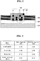
- the bifacial solar cell 100 may include a substrate 110 of a first conductive type, a first doped region 120 which is positioned at a first surface (for example, a front surface) of the substrate 110 and contains impurities of a second conductive type opposite the first conductive type, a first electrode part 140 which is positioned on the first doped region 120 and is electrically and/or physically connected to the first doped region 120, a second doped region 150 which is positioned at a second surface (for example, a back surface) opposite the first surface of the substrate 110 and contains impurities of the first conductive type at a concentration higher than the substrate 110, and a second electrode part 170 which is positioned on a back surface of the second doped region 150 and is electrically and/or physically connected to the second doped region 150.
- the substrate 110 may be formed of a silicon wafer of the first conductive type, for example, an n-type. Silicon used in the silicon wafer may be single crystal silicon, polycrystalline silicon, or amorphous silicon.
- the substrate 110 When the substrate 110 is of the n-type, the substrate 110 contains impurities of a group V element such as phosphorus (P), arsenic (As), and antimony (Sb).
- a group V element such as phosphorus (P), arsenic (As), and antimony (Sb).
- the substrate 110 may be formed of a silicon wafer of a p-type.
- the substrate 110 may contain impurities of a group III element such as boron (B), gallium (Ga), and indium (In).
- the substrate 110 may be of the n-type or the p-type.
- the embodiment of the invention is described using an n-type substrate as an example of the substrate 110.
- the first doped region 120 positioned at the front surface of the substrate 110 is an impurity region containing impurities of the p-type opposite the conductive type (for example, the n-type) of the substrate 110 and forms a p-n junction along with the substrate 110.
- the first doped region 120 forms an emitter region.
- the first doped region 120 may be formed by doping p-type impurities, for example, impurities of a group III element such as boron (B), gallium (Ga), and indium (In) on the first surface of the substrate 110 at a uniform concentration.
- impurities of a group III element such as boron (B), gallium (Ga), and indium (In)
- an impurity doping concentration of the first doped region 120 is uniform.
- the first doped region 120 may be formed by doping n-type impurities on the first surface of the substrate 110 at a uniform concentration.
- the first doped region 120 may be configured as a selective emitter region having different impurity doping concentrations depending on its position.
- an impurity doping concentration of the first doped region 120, on which the first electrode part 140 positioned on the first surface of the substrate 110 is formed may be different from an impurity doping concentration of the first doped region 120, on which the first electrode part 140 is not formed.
- the impurity doping concentration of the first doped region 120, on which the first electrode part 140 is formed may be higher or lower than the impurity doping concentration of the first doped region 120, on which the first electrode part 140 is not formed.
- Carriers i.e., electron-hole pairs produced by light incident on the substrate 110 are separated into electrons and holes by a built-in potential difference resulting from the p-n junction between the substrate 110 and the first doped region 120. Then, the separated electrons move to the n-type semiconductor, and the separated holes move to the p-type semiconductor.
- the separated electrons move to the n-type substrate 110, and the separated holes move to the first doped region 120.
- the electrons become major carriers in the n-type substrate 110, and the holes become major carriers in the first doped region 120.
- a front dielectric layer 130 may be formed on the first doped region 120.
- the front dielectric layer 130 may be formed of metal oxide-based material, for example, at least one of silicon nitride (SiNx), silicon oxide (SiOx), aluminum oxide (AlOx), and titanium dioxide (TiO 2 ).
- the front dielectric layer 130 may serve as an anti-reflection layer, which reduces a reflectance of light incident on the bifacial solar cell 100 through the first surface of the substrate 110 and increases selectivity of light of a predetermined wavelength band.
- the front dielectric layer 130 may serve as a passivation layer.
- the front dielectric layer 130 may not be formed on the first surface of the substrate 110.
- the front dielectric layer 130 When the front dielectric layer 130 is formed on the first surface of the substrate 110, the front dielectric layer 130 may include an opening exposing a portion of the first doped region 120.
- the first electrode part 140 is formed on the first doped region 120 exposed by the opening of the front dielectric layer 130.
- the first electrode part 140 may include a plurality of finger electrodes 140a extending in a first direction X-X' and a plurality of bus bar electrodes 140b extending in a second direction Y-Y' orthogonal to the first direction X-X'.
- the first electrode part 140 of the above-described configuration includes first conductive particles P1 for securing the electrical conductivity and second conductive particles P2 having a work function greater than the first conductive particles P1.
- the first conductive particles P1 are formed of silver (Ag) having excellent electrical conductivity, and the second conductive particles P2 are formed of nickel (Ni) capable of forming silicide NS at an interface contacting the first doped region 120.
- the first electrode part 140 further includes a resin R for securing an adhesive strength of the first and second conductive particles P1 and P2 with respect to the substrate 110.
- the resin R of the first electrode part 140 may be formed of a thermosetting resin including a monomer-based epoxy resin, an acrylic resin, etc.
- the first electrode part 140 of the above-described configuration is formed by printing, drying, and curing an electrode paste including the resin R and the first and second conductive particles P1 and P2 distributed in the resin R and then performing the silicidation of the electrode paste.
- the first electrode part 140 includes the first conductive particles P1 formed of silver (Ag) and the second conductive particles P2 formed of nickel (Ni), and nickel silicide (NiSi) is formed at the interface between the second conductive particles P2 and the first doped region 120.
- nickel (Ni) forming the second conductive particles P2 has a work function greater than silver (Ag) forming the first conductive particles P1.
- silver (Ag) has a work function of about 4.26 eV
- nickel (Ni) has a work function of about 5.10 eV which is greater than silver (Ag).
- Schottky barrier of silver (Ag) is about 0.89
- Schottky barrier of nickel (Ni) is about 0.05 which is much less than silver (Ag).
- a contact resistance between the first doped region 120 and the first electrode part 140 including the first conductive particles P1 and the second conductive particles P2 having the work function greater than the first conductive particles P1 is less than a contact resistance between the first doped region 120 and the first electrode part including only the first conductive particles P1.
- nickel silicide (NiSi) formed at the interface between the second conductive particles P2 and the first doped region 120 has a work function of about 4.82 eV and Schottky barrier of about 0.33. Therefore, nickel silicide (NiSi) has the work function less than nickel (Ni) and the Schottky barrier greater than nickel (Ni). However, nickel silicide (NiSi) has a specific resistance less than nickel (Ni).
- the contact resistance between the first doped region 120 and the first electrode part 140 is further reduced by nickel silicide (NiSi) formed at the interface between the second conductive particles P2 and the first doped region 120.
- NiSi nickel silicide
- Schottky barrier of a related art first electrode part including only first conductive particles has a first height ⁇ b1.
- Schottky barrier of the first electrode part 140 according to the embodiment of the invention including the first conductive particles P1, the second conductive particles P2, and nickel silicide (NiSi) has a second height ⁇ b2 which is less than the first height ⁇ b1 by a predetermined height ⁇ b.
- the first electrode part 140 includes about 15 wt% to 25 wt% of the nickel particles P2 based on the total weight of the silver particles P1 and the nickel particles P2.
- a specific resistance of the nickel particles P2 is about five times greater than a specific resistance of the silver particles P1
- the electrical characteristics of the solar cell when only the nickel particles P2 are used as the conductive particles distributed in the thermosetting resin R of the first electrode part 140 are reduced because of a very large line resistance of the first electrode part 140.
- the line resistance of the first electrode part 140 increases as an amount of nickel particles P2 increases.
- an amount of nickel particles P2 based on the total weight of the silver particles P1 and the nickel particles P2 is set in consideration of the line resistance of the first electrode part 140 and the contact resistance between the first doped region 120 and the first electrode part 140.
- the amount of nickel particles P2 is about 15 wt% to 25 wt% based on the total weight of the silver particles P1 and the nickel particles P2.
- an additive such as a distribution stabilizer, has to be used because it is difficult to efficiently distribute the nickel particles P2 in the resin R.
- the additive increases the line resistance of the first electrode part 140.
- the size of the nickel particles P2 may refer to a diameter.
- the nickel particles P2 may be efficiently distributed in the resin R by using the nickel particles P2 having the size expressed in the unit of micro.
- the size of the nickel particles P2 is about 2 ⁇ m to 10 ⁇ m.
- the first electrode part 140 of the above-described configuration collects carriers (for example, holes) moving to the first doped region 120.
- the second electrode part 170 positioned on the back surface of the substrate 110 collects carriers (for example, electrons) moving to the substrate 110 and outputs the carriers to an external device.
- carriers for example, electrons
- the second electrode part 170 includes a plurality of finger electrodes 170a formed at a location corresponding to the finger electrodes 140a of the first electrode part 140 and a plurality of bus bar electrodes 170b formed at a location corresponding to the bus bar electrodes 140b of the first electrode part 140.
- the number of finger electrodes 170a of the second electrode part 170 is more than the number of finger electrodes 140a of the first electrode part 140.
- the second electrode part 170 may be formed using the same electrode paste as the first electrode part 140.
- the second electrode part 170 may be formed by printing, drying, and curing the electrode paste including the resin R and the first and second conductive particles P1 and P2 distributed in the resin R.
- the second doped region 150 electrically and/or physically connected to the second electrode part 170 is positioned at the entire back surface of the substrate 110 and forms a potential barrier by a difference between impurity doping concentrations of the substrate 110 and the second doped region 150.
- the second doped region 150 serves as a back surface field region which prevents or reduces holes from moving to the back surface of the substrate 110. As a result, a recombination and/or a disappearance of electrons and holes at and around the surface of the substrate 110 are reduced.
- the second doped region 150 may be locally positioned at the back surface of the substrate 110, on which the second electrode part 170 is positioned, and may have a selective structure having different impurity doping concentrations in the same manner as the selective emitter region.
- an impurity doping concentration of the second doped region 150, on which the second electrode part 170 is positioned may be higher or lower than an impurity doping concentration of the second doped region 150, on which the second electrode part 170 is not positioned.
- silicide is formed at an interface between the second conductive particles P2 and the second doped region 150 in the same or similar manner as the first electrode part 140.
- the first doped region 120 shown in FIG. 2 may be the second doped region 150
- the front dielectric layer 130 may be a back dielectric layer 160 positioned on the back surface of the second doped region 150, on which the second electrode part 170 is not positioned.
- the back dielectric layer 160 may be formed of at least one of silicon nitride (SiNx), silicon oxide (SiOx), aluminum oxide (AlOx), and titanium dioxide (TiO 2 ) in the same manner as the front dielectric layer 130.
- the back dielectric layer 160 may be omitted if necessary or desired, in the same manner as the front dielectric layer 130.
- the front dielectric layer 130 When the front dielectric layer 130 is positioned on the front surface of the substrate 110 and the back dielectric layer 160 is positioned on the back surface of the substrate 110, the front dielectric layer 130 and the back dielectric layer 160 reduce a reflection loss of light incident on the substrate 110. Hence, an amount of light incident on the substrate 110 further increases.
- the electron-hole pairs are separated into electrons and holes by the p-n junction between the substrate 110 and the first doped region 120. Then, the separated electrons move to the n-type substrate 110, and the separated holes move to the p-type first doped region 120.
- the electrons moving to the substrate 110 move to the second electrode part 170 through the second doped region 150, and the holes moving to the first doped region 120 move to the first electrode part 140.
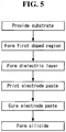
- FIG. 5 is a block diagram illustrating a method for manufacturing the solar cell shown in FIG. 1 .
- the first doped region 120 containing impurities of the second conductive type opposite the first conductive type is formed at the first surface of the substrate (for example, the n-type substrate 110) of the first conductive type.
- the first surface of the substrate 110 may be textured to form a textured surface corresponding to an uneven surface having a plurality of uneven portions or having uneven characteristics.
- the front dielectric layer 130 is formed on the first doped region 120.
- the front dielectric layer 130 may be formed using a chemical vapor deposition (CVD) method such as a plasma enhanced chemical vapor deposition (PECVD) method.
- CVD chemical vapor deposition
- PECVD plasma enhanced chemical vapor deposition
- the front dielectric layer 130 may have a single-layered structure or a multi-layered structure.
- the front dielectric layer 130 is partially etched to expose a portion of the first doped region 120, in which the first electrode part 140 is formed.
- the front dielectric layer 130 includes an opening exposing the portion of the first doped region 120.
- the opening may be formed in the same pattern (for example, a grid pattern) as the first electrode part 140.
- a laser may be used to form the opening in the front dielectric layer 130, but the embodiment of the invention is not limited thereto.
- a photolithography process may be used.
- an electrode paste for low temperature curing is printed and dried on the first doped region 120 exposed by the opening of the front dielectric layer 130.
- the embodiment of the invention is described as having the electrode paste printed and dried after forming the front dielectric layer 130.
- the electrode paste may be printed and dried in a state where the front dielectric layer 130 is not formed on the first doped region 120.
- the electrode paste for low temperature curing includes a thermosetting resin R, first conductive particles P1 distributed in the thermosetting resin R, and second conductive particles P2 which are distributed in the thermosetting resin R and having a work function greater than the first conductive particles P1, and forming silicide at an interface contacting the first doped region 120.
- the thermosetting resin R may include one of a monomer-based epoxy resin and an acrylic resin which are thermally processed and cured at a low temperature (for example, about 230 °C to 260 °C).
- the first conductive particles P1 may be silver (Ag) particles
- the second conductive particles P2 may be nickel (Ni) particles.
- a thermal process is performed on the electrode paste for low temperature curing at a low temperature of about 240 °C to cure the electrode paste.
- a thermal process which is performed at a temperature (for example, about 800 °C to 900 °C) higher than the electrode paste for low temperature curing according to the embodiment of the invention, has to be used to cure a related art electrode paste including a glass frit and first conductive particles (for example, Ag particles) distributed in the glass frit.
- a temperature for example, about 800 °C to 900 °C
- first conductive particles for example, Ag particles
- the electrode paste for low temperature curing does not include the glass frit including an etching component and includes the thermosetting resin R, which is cured at the low temperature (for example, about 230 °C to 260 °C), instead of the glass frit. Therefore, a heat damage applied to the first doped region 120 and the substrate 110 may be minimized. Hence, life time of a silicon bulk forming the substrate 110 increases, and an open-circuit voltage and a short circuit current density are improved. As a result, the efficiency of the solar cell may be improved.
- the substrate 110 is heated at the temperature of about 350 °C to 400 °C in an atmosphere of an inert gas to form silicide at the interface at which the second conductive particles P2 and the first doped region 120 contact each other.
- nickel silicide NiSi is formed at the interface contacting the first doped region 120.
- the method for manufacturing the bifacial solar cell according to the embodiment of the invention may include forming the first doped region at the first surface of the substrate and forming the second doped region at the second surface of the substrate, forming the front dielectric layer on the first surface of the substrate and forming the back dielectric layer on the second surface of the substrate, forming the opening in each of the front dielectric layer and the back dielectric layer, applying the electrode paste for forming the first electrode part to the first doped region exposed through the opening of the front dielectric layer and applying the electrode paste for forming the second electrode part to the second doped region exposed through the opening of the back dielectric layer, performing the thermal process on the electrode paste for the first electrode part and the electrode paste for the second electrode part at the low temperature to cure the electrode pastes, and forming silicide.
Description
- Embodiments of the invention relate to a solar cell and a method for manufacturing the same.
- Solar power generation to convert light energy into electric energy using a photoelectric conversion effect has been widely used as a method for obtaining eco-friendly energy. A solar power generation system using a plurality of solar cell modules has been installed in places, such as houses, due to an improvement in a photoelectric conversion efficiency of solar cells.
- The solar cell generally includes a substrate and an emitter region forming a p-n junction along with the substrate and generates electric current using light incident on a surface of the substrate.
-
EP 2 592 658 A1 relates to solar cells having a substrate with two differently doped silicon layers and an electrode. The electrode has a layered structure with two conductive layers 20a and 20b. Layer 20a contains a conductive material Da, which is preferably silver. Layer 20b is preferably any one of copper, gold, carbon, cobalt, titanium, nickel, and aluminum or a mixture thereof. -
US 2010/154875 A1 provides a method for making photovoltaic devices. An exchange metal is placed in contact with the silicon nitride layer on the substrate and a non-exchange metal is placed in contact with the exchange metal. -
WO 2010/019532 A2 relates to a method for making photovoltaic devices having transition metal silicides or rare earth metal silicides. - In one aspect, there is a solar cell including a substrate of a first conductive type, a first doped region which is positioned at a first surface of the substrate and contains impurities of a second conductive type opposite the first conductive type, and a first electrode part electrically connected to the first doped region, wherein the first electrode part includes a thermosetting resin, and first and second conductive particles distributed in the thermosetting resin, and the second conductive particles have a work function greater than the first conductive particles and form silicide at an interface contacting the first doped region.
- The first conductive particles are formed of silver (Ag) particles, and the second conductive particles are formed of nickel (Ni) particles. Silicide formed at an interface contacting a p+-type doped region is nickel silicide.
- The thermosetting resin of the first electrode part may include a monomer-based epoxy resin or an acrylic resin.
- The first doped region may be formed as an emitter region. A dielectric layer may be formed on the emitter region, on which the first electrode part is not positioned.
- The first electrode part may include a plurality of first finger electrodes extending in a first direction and a plurality of first bus bar electrodes extending in a second direction crossing the first finger electrodes.
- In another aspect, there is a method for manufacturing a solar cell including forming a first doped region containing impurities of a second conductive type opposite a first conductive type at a first surface of a substrate of the first conductive type, forming a dielectric layer having an opening exposing a portion of the first doped region on the first doped region, printing an electrode paste including a thermosetting resin, first conductive particles distributed in the thermosetting resin, and second conductive particles, which are distributed in the thermosetting resin, have a work function greater than the first conductive particles, performing a thermal process on the electrode paste at a low temperature to cure the electrode paste, and forming silicide at an interface at which the second conductive particles and the first doped region contact each other.
- The first conductive particles are silver (Ag), and the second conductive particles are nickel (Ni).
- Nickel silicide is formed at the interface, at which the second conductive particles and the first doped region contact each other, using the second conductive particles formed of nickel.
- The first doped region may be formed as an emitter region.
- In a general solar cell, an electrode part is formed by printing, drying, and curing a silver (Ag) paste containing aluminum (Al), and conductive particles (for example, Ag particles and Al particles) of the electrode part bring into contact with a doped region of a conductive type opposite a conductive type of a substrate due to an etching operation of a glass frit generated when the Ag paste is cured.
- As described above, when the electrode part is formed using the Ag paste containing aluminum (Al), a thermal process has to be performed on the Ag paste at a high temperature of about 800 °C to 900 °C.
- Accordingly, a defect inside a silicon bulk forming the substrate increases, and life time of the silicon bulk decreases. Further, an open-circuit voltage and a short circuit current density are reduced.
- To solve the above-described problems, a method for forming the electrode part using a silver paste for low temperature curing using a resin as a binder was recently developed.
- However, when the Ag paste for low temperature curing is used to form the electrode part, Schottky barrier resulting from a work function of silver increases. Hence, a contact resistance increases, and a fill factor of the solar cell increases.
- On the other hand, the electrode part according to the embodiment of the invention includes the first conductive particles (for example, silver (Ag) particles) and the second conductive particles (for example, nickel (Ni) particles) having the work function greater than the first conductive particles, and thus Schottky barrier of the electrode part is reduced. Hence, the contact resistance of the electrode part is reduced.
- Further, because silicide is formed at the interface, at which the second conductive particles and the doped region contact each other, the contact resistance of the electrode part is further reduced.
- The accompanying drawings, which are included to provide a further understanding of the disclosure and are incorporated in and constitute a part of this specification, illustrate embodiments of the invention and together with the description serve to explain the principles of the invention. In the drawings:
-
FIG. 1 is a perspective view of a main part of a solar cell according to an exemplary embodiment of the invention; -
FIG. 2 is a cross-sectional view of a main part of the solar cell shown inFIG. 1 ; -
FIG. 3 is a table indicating a work function and schottky barrier of each of various kinds of metals; -
FIG. 4 illustrates a difference between schottky barrier of a related art solar cell and schottky barrier of a solar cell according to an exemplary embodiment of the invention; and -
FIG. 5 is a block diagram illustrating a method for manufacturing the solar cell shown inFIG. 1 . - Reference will now be made in detail embodiments of the invention examples of which are illustrated in the accompanying drawings. Since the present invention may be modified in various ways and may have various forms, specific embodiments are illustrated in the drawings and are described in detail in the present specification.
- The terms 'first', 'second', etc., may be used to describe various components, but the components are not limited by such terms. The terms are used only for the purpose of distinguishing one component from other components.
- For example, a first component may be designated as a second component without departing from the scope of the present invention. In the same manner, the second component may be designated as the first component.
- The term "and/or" encompasses both combinations of the plurality of related items disclosed and any item from among the plurality of related items disclosed.
- When an arbitrary component is described as "being connected to" or "being linked to" another component, this should be understood to mean that still another component(s) may exist between them, although the arbitrary component may be directly connected to, or linked to, the second component.
- On the other hand, when an arbitrary component is described as "being directly connected to" or "being directly linked to" another component, this should be understood to mean that no component exists between them.
- The terms used in the present application are used to describe only specific embodiments or examples, and are not intended to limit the present invention. A singular expression can include a plural expression as long as it does not have an apparently different meaning in context.
- In the present application, the terms "include" and "have" should be understood to be intended to designate that illustrated features, numbers, steps, operations, components, parts or combinations thereof exist and do not preclude the existence of one or more different features, numbers, steps, operations, components, parts or combinations thereof, or the possibility of the addition thereof.
- In the drawings, the thickness of layers, films, panels, regions, etc., may be exaggerated for clarity. It will be understood that when an element such as a layer, film, region, or substrate is referred to as being "on" another element, it can be directly on the other element or intervening elements may also be present. In contrast, when an element is referred to as being "directly on" another element, there are no intervening elements present.
- Unless otherwise specified, all of the terms which are used herein, including the technical or scientific terms, may have the same meanings as those that are generally understood by a person having ordinary knowledge in the art.
- The terms defined in a generally used dictionary is understood to have meanings as those used in the context of a related art, and should not be construed to have ideal or excessively formal meanings unless they are obviously specified in the present application.
- The following exemplary embodiments of the invention are provided to those skilled in the art in order to provide the present disclosure more completely. Accordingly, shapes and sizes of elements shown in the drawings may be exaggerated for clarity.
- Exemplary embodiments of the invention will be described with reference to
FIGS. 1 to 5 . -
FIG. 1 is a perspective view of a main part of a solar cell according to an exemplary embodiment of the invention. More specifically,FIG. 1 is a perspective view of a main part of a bifacial solar cell. However, the embodiment of the invention is not limited to the bifacial solar cell and may be applied to solar cells of various structures. - A bifacial solar cell module including a plurality of bifacial
solar cells 100 includes an interconnector for electrically connecting the adjacent bifacialsolar cells 100, protective layers for protecting the bifacialsolar cells 100, a light transmission front substrate positioned on the protective layer at front surfaces of the bifacialsolar cells 100, and a light transmission back substrate positioned on a back surface of the protective layer at back surfaces of the bifacialsolar cells 100. - The light transmission front substrate and the light transmission back substrate prevent moisture or oxygen from penetrating the outside of the bifacial solar cell module, thereby protecting the bifacial
solar cells 100 from an external environment. - The light transmission front substrate and the light transmission back substrate are formed of a tempered glass having a high transmittance and an excellent damage prevention function. The tempered glass may be a low iron tempered glass containing a small amount of iron.
- The light transmission front substrate and the light transmission back substrate may have an embossed inner surface so as to increase a scattering effect of light.
- The light transmission front substrate and the light transmission back substrate may be formed of the low iron tempered glass or a polymer resin. In the embodiment disclosed herein, polyethylene terephthalate (PET) may be used as the polymer resin.
- A lamination process is performed on the protective layers in a state where the protective layers are respectively positioned on the front surfaces and the back surfaces of the bifacial
solar cells 100 to form an integral body of the protective layers and the bifacialsolar cells 100. Hence, the protective layers prevent corrosion of the bifacialsolar cells 100 resulting from the moisture penetration and protect the bifacialsolar cells 100 from an impact. - The protective layers may be formed of ethylene vinyl acetate (EVA) or silicon resin. However, other materials may be used.
- Referring to
FIG. 1 , the bifacialsolar cell 100 according to the embodiment of the invention may include asubstrate 110 of a first conductive type, a firstdoped region 120 which is positioned at a first surface (for example, a front surface) of thesubstrate 110 and contains impurities of a second conductive type opposite the first conductive type, afirst electrode part 140 which is positioned on the firstdoped region 120 and is electrically and/or physically connected to the firstdoped region 120, a seconddoped region 150 which is positioned at a second surface (for example, a back surface) opposite the first surface of thesubstrate 110 and contains impurities of the first conductive type at a concentration higher than thesubstrate 110, and asecond electrode part 170 which is positioned on a back surface of the seconddoped region 150 and is electrically and/or physically connected to the seconddoped region 150. - The
substrate 110 may be formed of a silicon wafer of the first conductive type, for example, an n-type. Silicon used in the silicon wafer may be single crystal silicon, polycrystalline silicon, or amorphous silicon. - When the
substrate 110 is of the n-type, thesubstrate 110 contains impurities of a group V element such as phosphorus (P), arsenic (As), and antimony (Sb). - Alternatively, the
substrate 110 may be formed of a silicon wafer of a p-type. In this instance, thesubstrate 110 may contain impurities of a group III element such as boron (B), gallium (Ga), and indium (In). - As described above, the
substrate 110 may be of the n-type or the p-type. In the following description, the embodiment of the invention is described using an n-type substrate as an example of thesubstrate 110. - The first
doped region 120 positioned at the front surface of thesubstrate 110 is an impurity region containing impurities of the p-type opposite the conductive type (for example, the n-type) of thesubstrate 110 and forms a p-n junction along with thesubstrate 110. Thus, in the embodiment of the invention, the firstdoped region 120 forms an emitter region. - When the
substrate 110 is the n-type substrate, the firstdoped region 120 may be formed by doping p-type impurities, for example, impurities of a group III element such as boron (B), gallium (Ga), and indium (In) on the first surface of thesubstrate 110 at a uniform concentration. Thus, in the embodiment of the invention, an impurity doping concentration of the firstdoped region 120 is uniform. - On the contrary, when the
substrate 110 is the p-type substrate, the firstdoped region 120 may be formed by doping n-type impurities on the first surface of thesubstrate 110 at a uniform concentration. - Alternatively, the first
doped region 120 may be configured as a selective emitter region having different impurity doping concentrations depending on its position. - In this instance, an impurity doping concentration of the first
doped region 120, on which thefirst electrode part 140 positioned on the first surface of thesubstrate 110 is formed, may be different from an impurity doping concentration of the firstdoped region 120, on which thefirst electrode part 140 is not formed. For example, the impurity doping concentration of the firstdoped region 120, on which thefirst electrode part 140 is formed, may be higher or lower than the impurity doping concentration of the firstdoped region 120, on which thefirst electrode part 140 is not formed. - Carriers, i.e., electron-hole pairs produced by light incident on the
substrate 110 are separated into electrons and holes by a built-in potential difference resulting from the p-n junction between thesubstrate 110 and the firstdoped region 120. Then, the separated electrons move to the n-type semiconductor, and the separated holes move to the p-type semiconductor. - Thus, the separated electrons move to the n-
type substrate 110, and the separated holes move to the firstdoped region 120. Hence, the electrons become major carriers in the n-type substrate 110, and the holes become major carriers in the firstdoped region 120. - A
front dielectric layer 130 may be formed on the firstdoped region 120. Thefront dielectric layer 130 may be formed of metal oxide-based material, for example, at least one of silicon nitride (SiNx), silicon oxide (SiOx), aluminum oxide (AlOx), and titanium dioxide (TiO2). Thefront dielectric layer 130 may serve as an anti-reflection layer, which reduces a reflectance of light incident on the bifacialsolar cell 100 through the first surface of thesubstrate 110 and increases selectivity of light of a predetermined wavelength band. In addition, thefront dielectric layer 130 may serve as a passivation layer. Alternatively, thefront dielectric layer 130 may not be formed on the first surface of thesubstrate 110. - When the
front dielectric layer 130 is formed on the first surface of thesubstrate 110, thefront dielectric layer 130 may include an opening exposing a portion of the firstdoped region 120. Thefirst electrode part 140 is formed on the firstdoped region 120 exposed by the opening of thefront dielectric layer 130. - The
first electrode part 140 may include a plurality offinger electrodes 140a extending in a first direction X-X' and a plurality ofbus bar electrodes 140b extending in a second direction Y-Y' orthogonal to the first direction X-X'. - The
first electrode part 140 of the above-described configuration includes first conductive particles P1 for securing the electrical conductivity and second conductive particles P2 having a work function greater than the first conductive particles P1. - The first conductive particles P1 are formed of silver (Ag) having excellent electrical conductivity, and the second conductive particles P2 are formed of nickel (Ni) capable of forming silicide NS at an interface contacting the first
doped region 120. - When the second conductive particles P2 are formed of nickel (Ni), nickel silicide (NiSi) is formed at the interface between the second conductive particles P2 and the first
doped region 120. Thefirst electrode part 140 further includes a resin R for securing an adhesive strength of the first and second conductive particles P1 and P2 with respect to thesubstrate 110. - The resin R of the
first electrode part 140 may be formed of a thermosetting resin including a monomer-based epoxy resin, an acrylic resin, etc. - The
first electrode part 140 of the above-described configuration is formed by printing, drying, and curing an electrode paste including the resin R and the first and second conductive particles P1 and P2 distributed in the resin R and then performing the silicidation of the electrode paste. - As described above, the
first electrode part 140 includes the first conductive particles P1 formed of silver (Ag) and the second conductive particles P2 formed of nickel (Ni), and nickel silicide (NiSi) is formed at the interface between the second conductive particles P2 and the firstdoped region 120. - However, as shown in
FIG. 3 , nickel (Ni) forming the second conductive particles P2 has a work function greater than silver (Ag) forming the first conductive particles P1. - More specifically, as shown in
FIG. 3 , silver (Ag) has a work function of about 4.26 eV, and nickel (Ni) has a work function of about 5.10 eV which is greater than silver (Ag). Further, when the n-type substrate 110 is formed of polycrystalline silicon, Schottky barrier of silver (Ag) is about 0.89, and Schottky barrier of nickel (Ni) is about 0.05 which is much less than silver (Ag). - Accordingly, a contact resistance between the first
doped region 120 and thefirst electrode part 140 including the first conductive particles P1 and the second conductive particles P2 having the work function greater than the first conductive particles P1, is less than a contact resistance between the firstdoped region 120 and the first electrode part including only the first conductive particles P1. - Further, nickel silicide (NiSi) formed at the interface between the second conductive particles P2 and the first
doped region 120 has a work function of about 4.82 eV and Schottky barrier of about 0.33. Therefore, nickel silicide (NiSi) has the work function less than nickel (Ni) and the Schottky barrier greater than nickel (Ni). However, nickel silicide (NiSi) has a specific resistance less than nickel (Ni). - Accordingly, the contact resistance between the first
doped region 120 and thefirst electrode part 140 is further reduced by nickel silicide (NiSi) formed at the interface between the second conductive particles P2 and the firstdoped region 120. - As shown in
FIG. 4 , Schottky barrier of a related art first electrode part including only first conductive particles has a first height Φb1. On the other hand, Schottky barrier of thefirst electrode part 140 according to the embodiment of the invention including the first conductive particles P1, the second conductive particles P2, and nickel silicide (NiSi) has a second height Φb2 which is less than the first height Φb1 by a predetermined height ΔΦb. - In the embodiment of the invention, when the first conductive particles P1 are formed of silver (Ag) and the second conductive particles P2 are formed of nickel (Ni), it is preferable that the
first electrode part 140 includes about 15 wt% to 25 wt% of the nickel particles P2 based on the total weight of the silver particles P1 and the nickel particles P2. - Because a specific resistance of the nickel particles P2 is about five times greater than a specific resistance of the silver particles P1, the electrical characteristics of the solar cell when only the nickel particles P2 are used as the conductive particles distributed in the thermosetting resin R of the
first electrode part 140, are reduced because of a very large line resistance of thefirst electrode part 140. - Alternatively, even when both the silver particles P1 and the nickel particles P2 are used as the conductive particles distributed in the thermosetting resin R, the line resistance of the
first electrode part 140 increases as an amount of nickel particles P2 increases. - Accordingly, it is preferable that an amount of nickel particles P2 based on the total weight of the silver particles P1 and the nickel particles P2 is set in consideration of the line resistance of the
first electrode part 140 and the contact resistance between the firstdoped region 120 and thefirst electrode part 140. - According to an experiment conducted by the present inventors, when the amount of nickel particles P2 was equal to or greater than about 25 wt% based on the total weight of the silver particles P1 and the nickel particles P2, the electrical characteristics of the solar cell were no longer improved even if the amount of nickel particles P2 further increased.
- When the amount of nickel particles P2 was less than about 15 wt% based on the total weight of the silver particles P1 and the nickel particles P2, it was difficult to efficiently reduce the height of the Schottky barrier of the
first electrode part 140. Further, because a small amount of nickel silicide (NiSi) was produced, an improvement effect of the contact resistance between the firstdoped region 120 and thefirst electrode part 140 was small. - Accordingly, it is preferable that the amount of nickel particles P2 is about 15 wt% to 25 wt% based on the total weight of the silver particles P1 and the nickel particles P2.
- When the size of the nickel particles P2 is very small (for example, when the size of the nickel particles P2 is expressed in the unit of nano), an additive, such as a distribution stabilizer, has to be used because it is difficult to efficiently distribute the nickel particles P2 in the resin R. However, the additive increases the line resistance of the
first electrode part 140. - In the embodiment disclosed herein, the size of the nickel particles P2 may refer to a diameter.
- Accordingly, even if the additive, such as the distribution stabilizer, is not used in the embodiment of the invention, the nickel particles P2 may be efficiently distributed in the resin R by using the nickel particles P2 having the size expressed in the unit of micro.
- For example, it is preferable that the size of the nickel particles P2 is about 2 µm to 10 µm.
- The
first electrode part 140 of the above-described configuration collects carriers (for example, holes) moving to the firstdoped region 120. - The
second electrode part 170 positioned on the back surface of thesubstrate 110 collects carriers (for example, electrons) moving to thesubstrate 110 and outputs the carriers to an external device. - In the embodiment of the invention, the
second electrode part 170 includes a plurality offinger electrodes 170a formed at a location corresponding to thefinger electrodes 140a of thefirst electrode part 140 and a plurality ofbus bar electrodes 170b formed at a location corresponding to thebus bar electrodes 140b of thefirst electrode part 140. - It is preferable that the number of
finger electrodes 170a of thesecond electrode part 170 is more than the number offinger electrodes 140a of thefirst electrode part 140. - The
second electrode part 170 may be formed using the same electrode paste as thefirst electrode part 140. In this instance, thesecond electrode part 170 may be formed by printing, drying, and curing the electrode paste including the resin R and the first and second conductive particles P1 and P2 distributed in the resin R. - The second
doped region 150 electrically and/or physically connected to thesecond electrode part 170 is positioned at the entire back surface of thesubstrate 110 and forms a potential barrier by a difference between impurity doping concentrations of thesubstrate 110 and the seconddoped region 150. Hence, the seconddoped region 150 serves as a back surface field region which prevents or reduces holes from moving to the back surface of thesubstrate 110. As a result, a recombination and/or a disappearance of electrons and holes at and around the surface of thesubstrate 110 are reduced. - Alternatively, the second
doped region 150 may be locally positioned at the back surface of thesubstrate 110, on which thesecond electrode part 170 is positioned, and may have a selective structure having different impurity doping concentrations in the same manner as the selective emitter region. - In the back surface field region having the selective structure, an impurity doping concentration of the second
doped region 150, on which thesecond electrode part 170 is positioned, may be higher or lower than an impurity doping concentration of the seconddoped region 150, on which thesecond electrode part 170 is not positioned. - When the
second electrode part 170 is formed using the electrode paste having the same configuration as the electrode paste forming thefirst electrode part 140, silicide is formed at an interface between the second conductive particles P2 and the seconddoped region 150 in the same or similar manner as thefirst electrode part 140. - In this instance, the first
doped region 120 shown inFIG. 2 may be the seconddoped region 150, and thefront dielectric layer 130 may be aback dielectric layer 160 positioned on the back surface of the seconddoped region 150, on which thesecond electrode part 170 is not positioned. - The
back dielectric layer 160 may be formed of at least one of silicon nitride (SiNx), silicon oxide (SiOx), aluminum oxide (AlOx), and titanium dioxide (TiO2) in the same manner as thefront dielectric layer 130. Theback dielectric layer 160 may be omitted if necessary or desired, in the same manner as thefront dielectric layer 130. - When light irradiated onto the bifacial
solar cell 100 having the above-described configuration is incident on thesubstrate 110 through the firstdoped region 120 and the seconddoped region 150, a plurality of electron-hole pairs are generated in thesubstrate 110 by light energy produced by the light incident on thesubstrate 110. - When the
front dielectric layer 130 is positioned on the front surface of thesubstrate 110 and theback dielectric layer 160 is positioned on the back surface of thesubstrate 110, thefront dielectric layer 130 and theback dielectric layer 160 reduce a reflection loss of light incident on thesubstrate 110. Hence, an amount of light incident on thesubstrate 110 further increases. - The electron-hole pairs are separated into electrons and holes by the p-n junction between the
substrate 110 and the firstdoped region 120. Then, the separated electrons move to the n-type substrate 110, and the separated holes move to the p-type first dopedregion 120. - As described above, the electrons moving to the
substrate 110 move to thesecond electrode part 170 through the seconddoped region 150, and the holes moving to the firstdoped region 120 move to thefirst electrode part 140. - Accordingly, when the
first electrode part 140 of one solar cell is connected to thesecond electrode part 170 of another solar cell adjacent to the one solar cell using electric wires, for example, the interconnector, electric current flows through the solar cells and allows use of the electric current for electric power. - A method for manufacturing the solar cell is described below.
FIG. 5 is a block diagram illustrating a method for manufacturing the solar cell shown inFIG. 1 . - First, the first
doped region 120 containing impurities of the second conductive type opposite the first conductive type is formed at the first surface of the substrate (for example, the n-type substrate 110) of the first conductive type. - Before forming the first
doped region 120, the first surface of thesubstrate 110 may be textured to form a textured surface corresponding to an uneven surface having a plurality of uneven portions or having uneven characteristics. - Next, the
front dielectric layer 130 is formed on the firstdoped region 120. Thefront dielectric layer 130 may be formed using a chemical vapor deposition (CVD) method such as a plasma enhanced chemical vapor deposition (PECVD) method. Thefront dielectric layer 130 may have a single-layered structure or a multi-layered structure. - After the
front dielectric layer 130 is formed, thefront dielectric layer 130 is partially etched to expose a portion of the firstdoped region 120, in which thefirst electrode part 140 is formed. When thefront dielectric layer 130 is partially etched, thefront dielectric layer 130 includes an opening exposing the portion of the firstdoped region 120. The opening may be formed in the same pattern (for example, a grid pattern) as thefirst electrode part 140. - A laser may be used to form the opening in the
front dielectric layer 130, but the embodiment of the invention is not limited thereto. A photolithography process may be used. - Next, an electrode paste for low temperature curing is printed and dried on the first
doped region 120 exposed by the opening of thefront dielectric layer 130. - The embodiment of the invention is described as having the electrode paste printed and dried after forming the
front dielectric layer 130. However, the electrode paste may be printed and dried in a state where thefront dielectric layer 130 is not formed on the firstdoped region 120. - The electrode paste for low temperature curing includes a thermosetting resin R, first conductive particles P1 distributed in the thermosetting resin R, and second conductive particles P2 which are distributed in the thermosetting resin R and having a work function greater than the first conductive particles P1, and forming silicide at an interface contacting the first
doped region 120. - In the embodiment disclosed herein, the thermosetting resin R may include one of a monomer-based epoxy resin and an acrylic resin which are thermally processed and cured at a low temperature (for example, about 230 °C to 260 °C). The first conductive particles P1 may be silver (Ag) particles, and the second conductive particles P2 may be nickel (Ni) particles.
- After the electrode paste for low temperature curing is dried, a thermal process is performed on the electrode paste for low temperature curing at a low temperature of about 240 °C to cure the electrode paste.
- A thermal process, which is performed at a temperature (for example, about 800 °C to 900 °C) higher than the electrode paste for low temperature curing according to the embodiment of the invention, has to be used to cure a related art electrode paste including a glass frit and first conductive particles (for example, Ag particles) distributed in the glass frit.
- On the other hand, the electrode paste for low temperature curing according to the embodiment of the invention does not include the glass frit including an etching component and includes the thermosetting resin R, which is cured at the low temperature (for example, about 230 °C to 260 °C), instead of the glass frit. Therefore, a heat damage applied to the first
doped region 120 and thesubstrate 110 may be minimized. Hence, life time of a silicon bulk forming thesubstrate 110 increases, and an open-circuit voltage and a short circuit current density are improved. As a result, the efficiency of the solar cell may be improved. - After the electrode paste for low temperature curing according to the embodiment of the invention is cured at the low temperature of about 230 °C to 260 °C, the
substrate 110 is heated at the temperature of about 350 °C to 400 °C in an atmosphere of an inert gas to form silicide at the interface at which the second conductive particles P2 and the firstdoped region 120 contact each other. - Because the embodiment of the invention is described using the nickel particles as the second conductive particles P2 as an example, nickel silicide (NiSi) is formed at the interface contacting the first
doped region 120. - The method for manufacturing the bifacial solar cell according to the embodiment of the invention may include forming the first doped region at the first surface of the substrate and forming the second doped region at the second surface of the substrate, forming the front dielectric layer on the first surface of the substrate and forming the back dielectric layer on the second surface of the substrate, forming the opening in each of the front dielectric layer and the back dielectric layer, applying the electrode paste for forming the first electrode part to the first doped region exposed through the opening of the front dielectric layer and applying the electrode paste for forming the second electrode part to the second doped region exposed through the opening of the back dielectric layer, performing the thermal process on the electrode paste for the first electrode part and the electrode paste for the second electrode part at the low temperature to cure the electrode pastes, and forming silicide.
Claims (11)
- A solar cell comprising:a substrate (110) of a first conductive type;a first doped region (120) positioned at a first surface of the substrate (110) and containing impurities of a second conductive type different from the first conductive type; anda first electrode part (140) electrically connected to the first doped region (120),wherein the first electrode part (140) includes a thermosetting resin (R), and first and second conductive particles (P1, P2) distributed in the thermosetting resin (R), and the second conductive particles (P2) have a work function greater than the first conductive particles (P1) and form silicide (NS) at an interface contacting the first doped region (120),characterized in that
the first conductive particles (P1) are formed of silver (Ag) particles, and the second conductive particles (P2) are formed of nickel (Ni) particles,
the formed silicide (NS) is nickel silicide (NS), and
the nickel particles (P2) are about 15 wt% to 25 wt% based on the total weight of the silver particles (P1) and the nickel particles (P2). - The solar cell of claim 1, wherein a size of a nickel particle (P2) is about 2 µm to 10 µm.
- The solar cell of claim 1, wherein the thermosetting resin (R) includes a monomer-based epoxy resin or an acrylic resin.
- The solar cell of claim 1, wherein the first doped region (120) is formed as an emitter region, and a dielectric layer (130) is formed on the emitter region (120).
- The solar cell of claim 4, wherein the first electrode part (140) includes a plurality of first finger electrodes (140a) extending in a first direction and a plurality of first bus bar electrodes (140b) extending in a second direction crossing the first finger electrodes.
- The solar cell of claim 1, further comprising:a second doped region (150) positioned at a second surface opposite the first surface of the substrate (110) and containing impurities of the first conductive type at a concentration higher than the substrate; anda second electrode part (170) electrically connected to the second doped region (160),wherein the second electrode part (170) includes the first conductive particles (P1), the second conductive particles (P2), silicide (NS), and the thermosetting resin (R).
- The solar cell of claim 6, wherein the second doped region (150) is formed as a back surface field region, and a dielectric layer (160) is formed on the back surface field region (150).
- The solar cell of claim 7, wherein the second electrode part (170) includes a plurality of second finger electrodes (170a) extending in a first direction and a plurality of second bus bar electrodes (170b) extending in a second direction crossing the second finger electrodes (170a).
- A method for manufacturing a solar cell comprising:forming a first doped region (120) containing impurities of a second conductive type different from a first conductive type at a first surface of a substrate (110) of the first conductive type;forming a dielectric layer (130) on the first doped region (120);forming an opening at the dielectric layer (130) to expose a portion of the first doped region (120);printing an electrode paste including a thermosetting resin (R), first conductive particles (P1) distributed in the thermosetting resin (R), and second conductive particles (P2) distributed in the thermosetting resin (R) and having a work function greater than the first conductive particles (P1);performing a thermal process on the electrode paste at a temperature to cure the electrode paste; andforming silicide (NS) at an interface at which the second conductive particles (P2) and the first doped region (120) contact each other,characterized in that
the first conductive particles (P1) are formed of silver (Ag) particles, and the second conductive particles (P2) are formed of nickel (Ni) particles,
the nickel particles (P2) are about 15 wt% to 25 wt% based on the total weight of the silver particles (P1) and the nickel particles (P2), and
wherein forming silicide comprises forming nickel silicide at the interface at which the second conductive particles and the first doped region contact each other, by using the second conductive particles formed of nickel. - The method of claim 9, wherein the thermal process performed on the electrode paste to cure the electrode paste is performed at a temperature of about 230 °C to 260 °C.
- The method of claim 10, wherein forming nickel silicide comprises heating the substrate at a temperature of about 350 °C to 400 °C.
Applications Claiming Priority (1)
| Application Number | Priority Date | Filing Date | Title |
|---|---|---|---|
| KR1020130056314A KR101614186B1 (en) | 2013-05-20 | 2013-05-20 | Solar cell and manufacturing method thereof |
Publications (3)
| Publication Number | Publication Date |
|---|---|
| EP2806465A2 EP2806465A2 (en) | 2014-11-26 |
| EP2806465A3 EP2806465A3 (en) | 2015-04-01 |
| EP2806465B1 true EP2806465B1 (en) | 2017-01-04 |
Family
ID=50390981
Family Applications (1)
| Application Number | Title | Priority Date | Filing Date |
|---|---|---|---|
| EP14001166.9A Active EP2806465B1 (en) | 2013-05-20 | 2014-03-28 | Solar cell and method for manufacturing the same |
Country Status (5)
| Country | Link |
|---|---|
| US (1) | US11004988B2 (en) |
| EP (1) | EP2806465B1 (en) |
| JP (1) | JP5952336B2 (en) |
| KR (1) | KR101614186B1 (en) |
| CN (1) | CN104183656B (en) |
Families Citing this family (4)
| Publication number | Priority date | Publication date | Assignee | Title |
|---|---|---|---|---|
| DE202015102238U1 (en) * | 2015-05-04 | 2015-06-01 | Solarworld Innovations Gmbh | Photovoltaic cell and photovoltaic module |
| CN116647677A (en) | 2016-10-28 | 2023-08-25 | 韩国电子通信研究院 | Video encoding/decoding method and apparatus, and recording medium storing bit stream |
| KR101980946B1 (en) * | 2016-11-11 | 2019-05-21 | 삼성에스디아이 주식회사 | Front electrode for solar cell and solar cell comprising the same |
| KR20210103850A (en) * | 2020-02-14 | 2021-08-24 | 엘지전자 주식회사 | Solar cell, and solar cell panel and method of manufacturing the same |
Family Cites Families (21)
| Publication number | Priority date | Publication date | Assignee | Title |
|---|---|---|---|---|
| JPS5896777A (en) | 1981-12-03 | 1983-06-08 | Mitsubishi Electric Corp | Solar battery |
| JP3254044B2 (en) | 1993-06-16 | 2002-02-04 | ナミックス株式会社 | Electrodes for solar cells |
| JP3557148B2 (en) | 2000-02-21 | 2004-08-25 | 三洋電機株式会社 | Solar cell module |
| US8575474B2 (en) | 2006-03-20 | 2013-11-05 | Heracus Precious Metals North America Conshohocken LLC | Solar cell contacts containing aluminum and at least one of boron, titanium, nickel, tin, silver, gallium, zinc, indium and copper |
| JP2008135654A (en) | 2006-11-29 | 2008-06-12 | Sanyo Electric Co Ltd | Solar battery module |
| TWI330998B (en) * | 2007-01-16 | 2010-09-21 | Chimei Innolux Corp | Top emitter organic electroluminescent display |
| JP4992449B2 (en) * | 2007-02-06 | 2012-08-08 | 株式会社村田製作所 | Thick film conductor composition and solar cell back Ag electrode |
| US20100037941A1 (en) | 2008-08-13 | 2010-02-18 | E. I. Du Pont De Nemours And Company | Compositions and processes for forming photovoltaic devices |
| CN101752452A (en) * | 2008-12-01 | 2010-06-23 | 台湾茂矽电子股份有限公司 | Method for manufacturing double-sided solar battery |
| US8710355B2 (en) | 2008-12-22 | 2014-04-29 | E I Du Pont De Nemours And Company | Compositions and processes for forming photovoltaic devices |
| JP2010182935A (en) * | 2009-02-06 | 2010-08-19 | Sharp Corp | Method of manufacturing thin film solar cell |
| JP5144857B2 (en) | 2010-03-01 | 2013-02-13 | 株式会社ノリタケカンパニーリミテド | Conductive paste composition for solar cell |
| TWI475702B (en) | 2010-07-09 | 2015-03-01 | Sakamoto Jun | A panel, a panel manufacturing method, a solar cell module, a printing apparatus, and a printing method |
| US20120037216A1 (en) | 2010-08-13 | 2012-02-16 | Samsung Electronics Co., Ltd. | Conductive paste and electronic device and solar cell including an electrode formed using the conductive paste |
| KR101665722B1 (en) | 2010-09-27 | 2016-10-24 | 엘지전자 주식회사 | Solar cell and manufacturing method thereof |
| TW201251084A (en) * | 2010-12-02 | 2012-12-16 | Applied Nanotech Holdings Inc | Nanoparticle inks for solar cells |
| KR20120079591A (en) | 2011-01-05 | 2012-07-13 | 엘지전자 주식회사 | Solar cell and manufacturing method thereof |
| KR20120091629A (en) * | 2011-02-09 | 2012-08-20 | 엘지전자 주식회사 | Solar cell |
| DE102011016335B4 (en) * | 2011-04-07 | 2013-10-02 | Universität Konstanz | Nickel-containing and corrosive printable paste and method for forming electrical contacts in the manufacture of a solar cell |
| US8901414B2 (en) * | 2011-09-14 | 2014-12-02 | International Business Machines Corporation | Photovoltaic cells with copper grid |
| CN104011882A (en) * | 2012-01-12 | 2014-08-27 | 应用材料公司 | Methods of manufacturing solar cell devices |
-
2013
- 2013-05-20 KR KR1020130056314A patent/KR101614186B1/en active IP Right Grant
-
2014
- 2014-03-20 US US14/221,111 patent/US11004988B2/en active Active
- 2014-03-28 EP EP14001166.9A patent/EP2806465B1/en active Active
- 2014-05-19 JP JP2014103448A patent/JP5952336B2/en active Active
- 2014-05-20 CN CN201410214046.3A patent/CN104183656B/en active Active
Non-Patent Citations (1)
| Title |
|---|
| None * |
Also Published As
| Publication number | Publication date |
|---|---|
| JP5952336B2 (en) | 2016-07-13 |
| US20140338738A1 (en) | 2014-11-20 |
| EP2806465A3 (en) | 2015-04-01 |
| CN104183656A (en) | 2014-12-03 |
| US11004988B2 (en) | 2021-05-11 |
| JP2014229904A (en) | 2014-12-08 |
| KR101614186B1 (en) | 2016-04-20 |
| CN104183656B (en) | 2017-01-18 |
| KR20140136562A (en) | 2014-12-01 |
| EP2806465A2 (en) | 2014-11-26 |
Similar Documents
| Publication | Publication Date | Title |
|---|---|---|
| US20110132426A1 (en) | Solar cell module | |
| US20190088805A1 (en) | Solar cell | |
| EP2889916B1 (en) | Solar cell and method for manufacturing the same | |
| WO2017002927A1 (en) | Solar battery and solar battery module | |
| EP2458649B1 (en) | Solar cell | |
| US10998456B2 (en) | Solar cell, method for manufacturing same and solar cell module | |
| US9337357B2 (en) | Bifacial solar cell module | |
| EP2711988B1 (en) | Solar cell and method for manufacturing the same | |
| EP2538447B1 (en) | Solar cell and method for manufacturing the same | |
| EP2806465B1 (en) | Solar cell and method for manufacturing the same | |
| CN114930542A (en) | Double-sided cascaded photovoltaic cells and modules | |
| US8420927B2 (en) | Solar cell, method of manufacturing the same, and solar cell module | |
| KR101092468B1 (en) | Solar cell and manufacturing mehtod of the same | |
| JP2013048146A (en) | Solar cell module | |
| KR101694553B1 (en) | Solar cell module | |
| US8507788B2 (en) | Solar cell panel | |
| EP2618386B1 (en) | Bifacial solar cell | |
| US20110132425A1 (en) | Solar cell module | |
| KR20150066131A (en) | Hetero junction solar cell and manufacturing method thereof | |
| JP6294694B2 (en) | SOLAR CELL, MANUFACTURING METHOD THEREOF, AND SOLAR CELL MODULE | |
| KR20150133567A (en) | Insulation substrate and manufacturing method of solar cell module with the same | |
| KR20150006941A (en) | Solar cell module | |
| WO2014148065A1 (en) | Solar cell |
Legal Events
| Date | Code | Title | Description |
|---|---|---|---|
| PUAI | Public reference made under article 153(3) epc to a published international application that has entered the european phase |
Free format text: ORIGINAL CODE: 0009012 |
|
| 17P | Request for examination filed |
Effective date: 20140328 |
|
| AK | Designated contracting states |
Kind code of ref document: A2 Designated state(s): AL AT BE BG CH CY CZ DE DK EE ES FI FR GB GR HR HU IE IS IT LI LT LU LV MC MK MT NL NO PL PT RO RS SE SI SK SM TR |
|
| AX | Request for extension of the european patent |
Extension state: BA ME |
|
| PUAL | Search report despatched |
Free format text: ORIGINAL CODE: 0009013 |
|
| AK | Designated contracting states |
Kind code of ref document: A3 Designated state(s): AL AT BE BG CH CY CZ DE DK EE ES FI FR GB GR HR HU IE IS IT LI LT LU LV MC MK MT NL NO PL PT RO RS SE SI SK SM TR |
|
| AX | Request for extension of the european patent |
Extension state: BA ME |
|
| RIC1 | Information provided on ipc code assigned before grant |
Ipc: H01L 31/068 20120101ALI20150223BHEP Ipc: H01L 31/0224 20060101AFI20150223BHEP Ipc: H01L 31/18 20060101ALI20150223BHEP |
|
| RBV | Designated contracting states (corrected) |
Designated state(s): AL AT BE BG CH CY CZ DE DK EE ES FI FR GB GR HR HU IE IS IT LI LT LU LV MC MK MT NL NO PL PT RO RS SE SI SK SM TR |
|
| 17Q | First examination report despatched |
Effective date: 20160218 |
|
| GRAP | Despatch of communication of intention to grant a patent |
Free format text: ORIGINAL CODE: EPIDOSNIGR1 |
|
| INTG | Intention to grant announced |
Effective date: 20160729 |
|
| GRAS | Grant fee paid |
Free format text: ORIGINAL CODE: EPIDOSNIGR3 |
|
| STAA | Information on the status of an ep patent application or granted ep patent |
Free format text: STATUS: GRANT OF PATENT IS INTENDED |
|
| GRAA | (expected) grant |
Free format text: ORIGINAL CODE: 0009210 |
|
| STAA | Information on the status of an ep patent application or granted ep patent |
Free format text: STATUS: THE PATENT HAS BEEN GRANTED |
|
| AK | Designated contracting states |
Kind code of ref document: B1 Designated state(s): AL AT BE BG CH CY CZ DE DK EE ES FI FR GB GR HR HU IE IS IT LI LT LU LV MC MK MT NL NO PL PT RO RS SE SI SK SM TR |
|
| REG | Reference to a national code |
Ref country code: GB Ref legal event code: FG4D |
|
| REG | Reference to a national code |
Ref country code: CH Ref legal event code: EP |
|
| REG | Reference to a national code |
Ref country code: AT Ref legal event code: REF Ref document number: 860008 Country of ref document: AT Kind code of ref document: T Effective date: 20170115 |
|
| REG | Reference to a national code |
Ref country code: NL Ref legal event code: FP |
|
| REG | Reference to a national code |
Ref country code: IE Ref legal event code: FG4D |
|
| REG | Reference to a national code |
Ref country code: DE Ref legal event code: R096 Ref document number: 602014005909 Country of ref document: DE |
|
| REG | Reference to a national code |
Ref country code: LT Ref legal event code: MG4D |
|
| REG | Reference to a national code |
Ref country code: AT Ref legal event code: MK05 Ref document number: 860008 Country of ref document: AT Kind code of ref document: T Effective date: 20170104 |
|
| PG25 | Lapsed in a contracting state [announced via postgrant information from national office to epo] |
Ref country code: IS Free format text: LAPSE BECAUSE OF FAILURE TO SUBMIT A TRANSLATION OF THE DESCRIPTION OR TO PAY THE FEE WITHIN THE PRESCRIBED TIME-LIMIT Effective date: 20170504 Ref country code: NO Free format text: LAPSE BECAUSE OF FAILURE TO SUBMIT A TRANSLATION OF THE DESCRIPTION OR TO PAY THE FEE WITHIN THE PRESCRIBED TIME-LIMIT Effective date: 20170404 Ref country code: HR Free format text: LAPSE BECAUSE OF FAILURE TO SUBMIT A TRANSLATION OF THE DESCRIPTION OR TO PAY THE FEE WITHIN THE PRESCRIBED TIME-LIMIT Effective date: 20170104 Ref country code: GR Free format text: LAPSE BECAUSE OF FAILURE TO SUBMIT A TRANSLATION OF THE DESCRIPTION OR TO PAY THE FEE WITHIN THE PRESCRIBED TIME-LIMIT Effective date: 20170405 Ref country code: LT Free format text: LAPSE BECAUSE OF FAILURE TO SUBMIT A TRANSLATION OF THE DESCRIPTION OR TO PAY THE FEE WITHIN THE PRESCRIBED TIME-LIMIT Effective date: 20170104 Ref country code: FI Free format text: LAPSE BECAUSE OF FAILURE TO SUBMIT A TRANSLATION OF THE DESCRIPTION OR TO PAY THE FEE WITHIN THE PRESCRIBED TIME-LIMIT Effective date: 20170104 |
|
| PG25 | Lapsed in a contracting state [announced via postgrant information from national office to epo] |
Ref country code: LV Free format text: LAPSE BECAUSE OF FAILURE TO SUBMIT A TRANSLATION OF THE DESCRIPTION OR TO PAY THE FEE WITHIN THE PRESCRIBED TIME-LIMIT Effective date: 20170104 Ref country code: ES Free format text: LAPSE BECAUSE OF FAILURE TO SUBMIT A TRANSLATION OF THE DESCRIPTION OR TO PAY THE FEE WITHIN THE PRESCRIBED TIME-LIMIT Effective date: 20170104 Ref country code: SE Free format text: LAPSE BECAUSE OF FAILURE TO SUBMIT A TRANSLATION OF THE DESCRIPTION OR TO PAY THE FEE WITHIN THE PRESCRIBED TIME-LIMIT Effective date: 20170104 Ref country code: BG Free format text: LAPSE BECAUSE OF FAILURE TO SUBMIT A TRANSLATION OF THE DESCRIPTION OR TO PAY THE FEE WITHIN THE PRESCRIBED TIME-LIMIT Effective date: 20170404 Ref country code: PT Free format text: LAPSE BECAUSE OF FAILURE TO SUBMIT A TRANSLATION OF THE DESCRIPTION OR TO PAY THE FEE WITHIN THE PRESCRIBED TIME-LIMIT Effective date: 20170504 Ref country code: RS Free format text: LAPSE BECAUSE OF FAILURE TO SUBMIT A TRANSLATION OF THE DESCRIPTION OR TO PAY THE FEE WITHIN THE PRESCRIBED TIME-LIMIT Effective date: 20170104 Ref country code: PL Free format text: LAPSE BECAUSE OF FAILURE TO SUBMIT A TRANSLATION OF THE DESCRIPTION OR TO PAY THE FEE WITHIN THE PRESCRIBED TIME-LIMIT Effective date: 20170104 Ref country code: AT Free format text: LAPSE BECAUSE OF FAILURE TO SUBMIT A TRANSLATION OF THE DESCRIPTION OR TO PAY THE FEE WITHIN THE PRESCRIBED TIME-LIMIT Effective date: 20170104 |
|
| REG | Reference to a national code |
Ref country code: DE Ref legal event code: R097 Ref document number: 602014005909 Country of ref document: DE |
|
| PG25 | Lapsed in a contracting state [announced via postgrant information from national office to epo] |
Ref country code: EE Free format text: LAPSE BECAUSE OF FAILURE TO SUBMIT A TRANSLATION OF THE DESCRIPTION OR TO PAY THE FEE WITHIN THE PRESCRIBED TIME-LIMIT Effective date: 20170104 Ref country code: RO Free format text: LAPSE BECAUSE OF FAILURE TO SUBMIT A TRANSLATION OF THE DESCRIPTION OR TO PAY THE FEE WITHIN THE PRESCRIBED TIME-LIMIT Effective date: 20170104 Ref country code: CZ Free format text: LAPSE BECAUSE OF FAILURE TO SUBMIT A TRANSLATION OF THE DESCRIPTION OR TO PAY THE FEE WITHIN THE PRESCRIBED TIME-LIMIT Effective date: 20170104 Ref country code: SK Free format text: LAPSE BECAUSE OF FAILURE TO SUBMIT A TRANSLATION OF THE DESCRIPTION OR TO PAY THE FEE WITHIN THE PRESCRIBED TIME-LIMIT Effective date: 20170104 |
|
| REG | Reference to a national code |
Ref country code: CH Ref legal event code: PL |
|
| PLBE | No opposition filed within time limit |
Free format text: ORIGINAL CODE: 0009261 |
|
| STAA | Information on the status of an ep patent application or granted ep patent |
Free format text: STATUS: NO OPPOSITION FILED WITHIN TIME LIMIT |
|
| PG25 | Lapsed in a contracting state [announced via postgrant information from national office to epo] |
Ref country code: DK Free format text: LAPSE BECAUSE OF FAILURE TO SUBMIT A TRANSLATION OF THE DESCRIPTION OR TO PAY THE FEE WITHIN THE PRESCRIBED TIME-LIMIT Effective date: 20170104 Ref country code: SM Free format text: LAPSE BECAUSE OF FAILURE TO SUBMIT A TRANSLATION OF THE DESCRIPTION OR TO PAY THE FEE WITHIN THE PRESCRIBED TIME-LIMIT Effective date: 20170104 Ref country code: MC Free format text: LAPSE BECAUSE OF FAILURE TO SUBMIT A TRANSLATION OF THE DESCRIPTION OR TO PAY THE FEE WITHIN THE PRESCRIBED TIME-LIMIT Effective date: 20170104 |
|
| REG | Reference to a national code |
Ref country code: IE Ref legal event code: MM4A |
|
| REG | Reference to a national code |
Ref country code: FR Ref legal event code: ST Effective date: 20171130 |
|
| PG25 | Lapsed in a contracting state [announced via postgrant information from national office to epo] |
Ref country code: LU Free format text: LAPSE BECAUSE OF NON-PAYMENT OF DUE FEES Effective date: 20170328 Ref country code: FR Free format text: LAPSE BECAUSE OF NON-PAYMENT OF DUE FEES Effective date: 20170331 |
|
| PG25 | Lapsed in a contracting state [announced via postgrant information from national office to epo] |
Ref country code: CH Free format text: LAPSE BECAUSE OF NON-PAYMENT OF DUE FEES Effective date: 20170331 Ref country code: IE Free format text: LAPSE BECAUSE OF NON-PAYMENT OF DUE FEES Effective date: 20170328 Ref country code: SI Free format text: LAPSE BECAUSE OF FAILURE TO SUBMIT A TRANSLATION OF THE DESCRIPTION OR TO PAY THE FEE WITHIN THE PRESCRIBED TIME-LIMIT Effective date: 20170104 Ref country code: LI Free format text: LAPSE BECAUSE OF NON-PAYMENT OF DUE FEES Effective date: 20170331 |
|
| REG | Reference to a national code |
Ref country code: BE Ref legal event code: MM Effective date: 20170331 |
|
| PGFP | Annual fee paid to national office [announced via postgrant information from national office to epo] |
Ref country code: NL Payment date: 20180207 Year of fee payment: 5 |
|
| PG25 | Lapsed in a contracting state [announced via postgrant information from national office to epo] |
Ref country code: BE Free format text: LAPSE BECAUSE OF NON-PAYMENT OF DUE FEES Effective date: 20170331 |
|
| PGFP | Annual fee paid to national office [announced via postgrant information from national office to epo] |
Ref country code: IT Payment date: 20180315 Year of fee payment: 5 |
|
| PG25 | Lapsed in a contracting state [announced via postgrant information from national office to epo] |
Ref country code: MT Free format text: LAPSE BECAUSE OF NON-PAYMENT OF DUE FEES Effective date: 20170328 |
|
| GBPC | Gb: european patent ceased through non-payment of renewal fee |
Effective date: 20180328 |
|
| PG25 | Lapsed in a contracting state [announced via postgrant information from national office to epo] |
Ref country code: GB Free format text: LAPSE BECAUSE OF NON-PAYMENT OF DUE FEES Effective date: 20180328 |
|
| PG25 | Lapsed in a contracting state [announced via postgrant information from national office to epo] |
Ref country code: HU Free format text: LAPSE BECAUSE OF FAILURE TO SUBMIT A TRANSLATION OF THE DESCRIPTION OR TO PAY THE FEE WITHIN THE PRESCRIBED TIME-LIMIT; INVALID AB INITIO Effective date: 20140328 |
|
| PG25 | Lapsed in a contracting state [announced via postgrant information from national office to epo] |
Ref country code: CY Free format text: LAPSE BECAUSE OF FAILURE TO SUBMIT A TRANSLATION OF THE DESCRIPTION OR TO PAY THE FEE WITHIN THE PRESCRIBED TIME-LIMIT Effective date: 20170104 |
|
| REG | Reference to a national code |
Ref country code: NL Ref legal event code: MM Effective date: 20190401 |
|
| PG25 | Lapsed in a contracting state [announced via postgrant information from national office to epo] |
Ref country code: MK Free format text: LAPSE BECAUSE OF FAILURE TO SUBMIT A TRANSLATION OF THE DESCRIPTION OR TO PAY THE FEE WITHIN THE PRESCRIBED TIME-LIMIT Effective date: 20170104 |
|
| PG25 | Lapsed in a contracting state [announced via postgrant information from national office to epo] |
Ref country code: NL Free format text: LAPSE BECAUSE OF NON-PAYMENT OF DUE FEES Effective date: 20190401 |
|
| PG25 | Lapsed in a contracting state [announced via postgrant information from national office to epo] |
Ref country code: IT Free format text: LAPSE BECAUSE OF NON-PAYMENT OF DUE FEES Effective date: 20190328 |
|
| PG25 | Lapsed in a contracting state [announced via postgrant information from national office to epo] |
Ref country code: TR Free format text: LAPSE BECAUSE OF FAILURE TO SUBMIT A TRANSLATION OF THE DESCRIPTION OR TO PAY THE FEE WITHIN THE PRESCRIBED TIME-LIMIT Effective date: 20170104 |
|
| PG25 | Lapsed in a contracting state [announced via postgrant information from national office to epo] |
Ref country code: AL Free format text: LAPSE BECAUSE OF FAILURE TO SUBMIT A TRANSLATION OF THE DESCRIPTION OR TO PAY THE FEE WITHIN THE PRESCRIBED TIME-LIMIT Effective date: 20170104 |
|
| REG | Reference to a national code |
Ref country code: DE Ref legal event code: R081 Ref document number: 602014005909 Country of ref document: DE Owner name: SHANGRAO JINKO SOLAR TECHNOLOGY DEVELOPMENT CO, CN Free format text: FORMER OWNER: LG ELECTRONICS INC., SEOUL, KR Ref country code: DE Ref legal event code: R082 Ref document number: 602014005909 Country of ref document: DE Representative=s name: DREISS PATENTANWAELTE PARTG MBB, DE Ref country code: DE Ref legal event code: R082 Ref document number: 602014005909 Country of ref document: DE Representative=s name: MANITZ FINSTERWALD PATENT- UND RECHTSANWALTSPA, DE Ref country code: DE Ref legal event code: R081 Ref document number: 602014005909 Country of ref document: DE Owner name: TRINA SOLAR CO., LTD., CHANGZHOU, CN Free format text: FORMER OWNER: LG ELECTRONICS INC., SEOUL, KR Ref country code: DE Ref legal event code: R081 Ref document number: 602014005909 Country of ref document: DE Owner name: SHANGRAO XINYUAN YUEDONG TECHNOLOGY DEVELOPMEN, CN Free format text: FORMER OWNER: LG ELECTRONICS INC., SEOUL, KR |
|
| PGFP | Annual fee paid to national office [announced via postgrant information from national office to epo] |
Ref country code: DE Payment date: 20230321 Year of fee payment: 10 |
|
| REG | Reference to a national code |
Ref country code: DE Ref legal event code: R081 Ref document number: 602014005909 Country of ref document: DE Owner name: TRINA SOLAR CO., LTD., CHANGZHOU, CN Free format text: FORMER OWNER: SHANGRAO JINKO SOLAR TECHNOLOGY DEVELOPMENT CO., LTD, SHANGRAO, JIANGXI PROVINCE, CN Ref country code: DE Ref legal event code: R081 Ref document number: 602014005909 Country of ref document: DE Owner name: SHANGRAO XINYUAN YUEDONG TECHNOLOGY DEVELOPMEN, CN Free format text: FORMER OWNER: SHANGRAO JINKO SOLAR TECHNOLOGY DEVELOPMENT CO., LTD, SHANGRAO, JIANGXI PROVINCE, CN |
|
| REG | Reference to a national code |
Ref country code: DE Ref legal event code: R082 Ref document number: 602014005909 Country of ref document: DE Representative=s name: MANITZ FINSTERWALD PATENT- UND RECHTSANWALTSPA, DE Ref country code: DE Ref legal event code: R081 Ref document number: 602014005909 Country of ref document: DE Owner name: TRINA SOLAR CO., LTD., CHANGZHOU, CN Free format text: FORMER OWNER: SHANGRAO XINYUAN YUEDONG TECHNOLOGY DEVELOPMENT CO. LTD, SHANGRAO, JIANGXI PROVINCE, CN |