JP5952336B2 - Solar cell and manufacturing method thereof - Google Patents
Solar cell and manufacturing method thereof Download PDFInfo
- Publication number
- JP5952336B2 JP5952336B2 JP2014103448A JP2014103448A JP5952336B2 JP 5952336 B2 JP5952336 B2 JP 5952336B2 JP 2014103448 A JP2014103448 A JP 2014103448A JP 2014103448 A JP2014103448 A JP 2014103448A JP 5952336 B2 JP5952336 B2 JP 5952336B2
- Authority
- JP
- Japan
- Prior art keywords
- conductive particles
- solar cell
- doping
- nickel
- electrode
- Prior art date
- Legal status (The legal status is an assumption and is not a legal conclusion. Google has not performed a legal analysis and makes no representation as to the accuracy of the status listed.)
- Active
Links
- 238000004519 manufacturing process Methods 0.000 title claims description 14
- PXHVJJICTQNCMI-UHFFFAOYSA-N Nickel Chemical compound [Ni] PXHVJJICTQNCMI-UHFFFAOYSA-N 0.000 claims description 129
- 239000002245 particle Substances 0.000 claims description 80
- 239000000758 substrate Substances 0.000 claims description 80
- 229910052759 nickel Inorganic materials 0.000 claims description 48
- BQCADISMDOOEFD-UHFFFAOYSA-N Silver Chemical compound [Ag] BQCADISMDOOEFD-UHFFFAOYSA-N 0.000 claims description 36
- 229910052709 silver Inorganic materials 0.000 claims description 31
- 239000004332 silver Substances 0.000 claims description 31
- 229920005989 resin Polymers 0.000 claims description 29
- 239000011347 resin Substances 0.000 claims description 29
- RUFLMLWJRZAWLJ-UHFFFAOYSA-N nickel silicide Chemical compound [Ni]=[Si]=[Ni] RUFLMLWJRZAWLJ-UHFFFAOYSA-N 0.000 claims description 27
- 229910021334 nickel silicide Inorganic materials 0.000 claims description 27
- 239000002003 electrode paste Substances 0.000 claims description 23
- 239000012535 impurity Substances 0.000 claims description 23
- 229920001187 thermosetting polymer Polymers 0.000 claims description 18
- 238000000034 method Methods 0.000 claims description 16
- 229910021332 silicide Inorganic materials 0.000 claims description 15
- FVBUAEGBCNSCDD-UHFFFAOYSA-N silicide(4-) Chemical compound [Si-4] FVBUAEGBCNSCDD-UHFFFAOYSA-N 0.000 claims description 15
- 230000004888 barrier function Effects 0.000 claims description 13
- 238000010438 heat treatment Methods 0.000 claims description 8
- 239000004925 Acrylic resin Substances 0.000 claims description 4
- 229920000178 Acrylic resin Polymers 0.000 claims description 4
- 230000005684 electric field Effects 0.000 claims description 4
- 239000003822 epoxy resin Substances 0.000 claims description 4
- 229920000647 polyepoxide Polymers 0.000 claims description 4
- 239000010410 layer Substances 0.000 description 34
- 230000008569 process Effects 0.000 description 8
- XEEYBQQBJWHFJM-UHFFFAOYSA-N Iron Chemical compound [Fe] XEEYBQQBJWHFJM-UHFFFAOYSA-N 0.000 description 6
- XUIMIQQOPSSXEZ-UHFFFAOYSA-N Silicon Chemical compound [Si] XUIMIQQOPSSXEZ-UHFFFAOYSA-N 0.000 description 6
- 239000011521 glass Substances 0.000 description 6
- 230000001681 protective effect Effects 0.000 description 6
- 229910052710 silicon Inorganic materials 0.000 description 6
- 239000010703 silicon Substances 0.000 description 6
- VYPSYNLAJGMNEJ-UHFFFAOYSA-N Silicium dioxide Chemical compound O=[Si]=O VYPSYNLAJGMNEJ-UHFFFAOYSA-N 0.000 description 4
- GWEVSGVZZGPLCZ-UHFFFAOYSA-N Titan oxide Chemical compound O=[Ti]=O GWEVSGVZZGPLCZ-UHFFFAOYSA-N 0.000 description 4
- 229910052814 silicon oxide Inorganic materials 0.000 description 4
- 239000005341 toughened glass Substances 0.000 description 4
- 230000009471 action Effects 0.000 description 3
- 229910052782 aluminium Inorganic materials 0.000 description 3
- XAGFODPZIPBFFR-UHFFFAOYSA-N aluminium Chemical compound [Al] XAGFODPZIPBFFR-UHFFFAOYSA-N 0.000 description 3
- 238000001035 drying Methods 0.000 description 3
- 230000000694 effects Effects 0.000 description 3
- 239000005038 ethylene vinyl acetate Substances 0.000 description 3
- 229910052742 iron Inorganic materials 0.000 description 3
- 229910052751 metal Inorganic materials 0.000 description 3
- 239000002184 metal Substances 0.000 description 3
- 239000000178 monomer Substances 0.000 description 3
- ZOXJGFHDIHLPTG-UHFFFAOYSA-N Boron Chemical compound [B] ZOXJGFHDIHLPTG-UHFFFAOYSA-N 0.000 description 2
- GYHNNYVSQQEPJS-UHFFFAOYSA-N Gallium Chemical compound [Ga] GYHNNYVSQQEPJS-UHFFFAOYSA-N 0.000 description 2
- 229910052581 Si3N4 Inorganic materials 0.000 description 2
- 229910004205 SiNX Inorganic materials 0.000 description 2
- 229910010413 TiO 2 Inorganic materials 0.000 description 2
- 239000000654 additive Substances 0.000 description 2
- 229910052796 boron Inorganic materials 0.000 description 2
- DQXBYHZEEUGOBF-UHFFFAOYSA-N but-3-enoic acid;ethene Chemical compound C=C.OC(=O)CC=C DQXBYHZEEUGOBF-UHFFFAOYSA-N 0.000 description 2
- 239000000969 carrier Substances 0.000 description 2
- 238000006243 chemical reaction Methods 0.000 description 2
- 238000005229 chemical vapour deposition Methods 0.000 description 2
- 230000007423 decrease Effects 0.000 description 2
- 230000003247 decreasing effect Effects 0.000 description 2
- 238000010586 diagram Methods 0.000 description 2
- 239000006185 dispersion Substances 0.000 description 2
- 238000005530 etching Methods 0.000 description 2
- 229910052733 gallium Inorganic materials 0.000 description 2
- 230000014509 gene expression Effects 0.000 description 2
- 229910052738 indium Inorganic materials 0.000 description 2
- APFVFJFRJDLVQX-UHFFFAOYSA-N indium atom Chemical compound [In] APFVFJFRJDLVQX-UHFFFAOYSA-N 0.000 description 2
- 239000000463 material Substances 0.000 description 2
- 238000012986 modification Methods 0.000 description 2
- 230000004048 modification Effects 0.000 description 2
- TWNQGVIAIRXVLR-UHFFFAOYSA-N oxo(oxoalumanyloxy)alumane Chemical compound O=[Al]O[Al]=O TWNQGVIAIRXVLR-UHFFFAOYSA-N 0.000 description 2
- 238000000623 plasma-assisted chemical vapour deposition Methods 0.000 description 2
- 229920001200 poly(ethylene-vinyl acetate) Polymers 0.000 description 2
- 229910021420 polycrystalline silicon Inorganic materials 0.000 description 2
- -1 polyethylene terephthalate Polymers 0.000 description 2
- 229920000139 polyethylene terephthalate Polymers 0.000 description 2
- 239000005020 polyethylene terephthalate Substances 0.000 description 2
- 239000002952 polymeric resin Substances 0.000 description 2
- 238000010248 power generation Methods 0.000 description 2
- HQVNEWCFYHHQES-UHFFFAOYSA-N silicon nitride Chemical compound N12[Si]34N5[Si]62N3[Si]51N64 HQVNEWCFYHHQES-UHFFFAOYSA-N 0.000 description 2
- 239000003381 stabilizer Substances 0.000 description 2
- 229920003002 synthetic resin Polymers 0.000 description 2
- 239000004408 titanium dioxide Substances 0.000 description 2
- OAICVXFJPJFONN-UHFFFAOYSA-N Phosphorus Chemical compound [P] OAICVXFJPJFONN-UHFFFAOYSA-N 0.000 description 1
- 230000000996 additive effect Effects 0.000 description 1
- 229910021417 amorphous silicon Inorganic materials 0.000 description 1
- 229910052787 antimony Inorganic materials 0.000 description 1
- WATWJIUSRGPENY-UHFFFAOYSA-N antimony atom Chemical compound [Sb] WATWJIUSRGPENY-UHFFFAOYSA-N 0.000 description 1
- 238000000149 argon plasma sintering Methods 0.000 description 1
- 229910052785 arsenic Inorganic materials 0.000 description 1
- RQNWIZPPADIBDY-UHFFFAOYSA-N arsenic atom Chemical compound [As] RQNWIZPPADIBDY-UHFFFAOYSA-N 0.000 description 1
- 239000011230 binding agent Substances 0.000 description 1
- 239000004020 conductor Substances 0.000 description 1
- 230000007797 corrosion Effects 0.000 description 1
- 238000005260 corrosion Methods 0.000 description 1
- 230000006378 damage Effects 0.000 description 1
- 230000007547 defect Effects 0.000 description 1
- 238000002474 experimental method Methods 0.000 description 1
- 230000006872 improvement Effects 0.000 description 1
- 239000011261 inert gas Substances 0.000 description 1
- 238000010030 laminating Methods 0.000 description 1
- 229910044991 metal oxide Inorganic materials 0.000 description 1
- 150000004706 metal oxides Chemical class 0.000 description 1
- 150000002739 metals Chemical class 0.000 description 1
- 229910021421 monocrystalline silicon Inorganic materials 0.000 description 1
- 238000002161 passivation Methods 0.000 description 1
- 230000035515 penetration Effects 0.000 description 1
- 229910052698 phosphorus Inorganic materials 0.000 description 1
- 239000011574 phosphorus Substances 0.000 description 1
- 238000000206 photolithography Methods 0.000 description 1
- 238000005036 potential barrier Methods 0.000 description 1
- 230000002265 prevention Effects 0.000 description 1
- 230000006798 recombination Effects 0.000 description 1
- 238000005215 recombination Methods 0.000 description 1
- 239000002356 single layer Substances 0.000 description 1
- 230000003685 thermal hair damage Effects 0.000 description 1
- 238000002834 transmittance Methods 0.000 description 1
Images


Classifications
-
- H—ELECTRICITY
- H01—ELECTRIC ELEMENTS
- H01L—SEMICONDUCTOR DEVICES NOT COVERED BY CLASS H10
- H01L31/00—Semiconductor devices sensitive to infrared radiation, light, electromagnetic radiation of shorter wavelength or corpuscular radiation and specially adapted either for the conversion of the energy of such radiation into electrical energy or for the control of electrical energy by such radiation; Processes or apparatus specially adapted for the manufacture or treatment thereof or of parts thereof; Details thereof
- H01L31/02—Details
- H01L31/0224—Electrodes
- H01L31/022408—Electrodes for devices characterised by at least one potential jump barrier or surface barrier
- H01L31/022425—Electrodes for devices characterised by at least one potential jump barrier or surface barrier for solar cells
-
- H—ELECTRICITY
- H01—ELECTRIC ELEMENTS
- H01L—SEMICONDUCTOR DEVICES NOT COVERED BY CLASS H10
- H01L31/00—Semiconductor devices sensitive to infrared radiation, light, electromagnetic radiation of shorter wavelength or corpuscular radiation and specially adapted either for the conversion of the energy of such radiation into electrical energy or for the control of electrical energy by such radiation; Processes or apparatus specially adapted for the manufacture or treatment thereof or of parts thereof; Details thereof
- H01L31/04—Semiconductor devices sensitive to infrared radiation, light, electromagnetic radiation of shorter wavelength or corpuscular radiation and specially adapted either for the conversion of the energy of such radiation into electrical energy or for the control of electrical energy by such radiation; Processes or apparatus specially adapted for the manufacture or treatment thereof or of parts thereof; Details thereof adapted as photovoltaic [PV] conversion devices
- H01L31/06—Semiconductor devices sensitive to infrared radiation, light, electromagnetic radiation of shorter wavelength or corpuscular radiation and specially adapted either for the conversion of the energy of such radiation into electrical energy or for the control of electrical energy by such radiation; Processes or apparatus specially adapted for the manufacture or treatment thereof or of parts thereof; Details thereof adapted as photovoltaic [PV] conversion devices characterised by at least one potential-jump barrier or surface barrier
- H01L31/068—Semiconductor devices sensitive to infrared radiation, light, electromagnetic radiation of shorter wavelength or corpuscular radiation and specially adapted either for the conversion of the energy of such radiation into electrical energy or for the control of electrical energy by such radiation; Processes or apparatus specially adapted for the manufacture or treatment thereof or of parts thereof; Details thereof adapted as photovoltaic [PV] conversion devices characterised by at least one potential-jump barrier or surface barrier the potential barriers being only of the PN homojunction type, e.g. bulk silicon PN homojunction solar cells or thin film polycrystalline silicon PN homojunction solar cells
- H01L31/0684—Semiconductor devices sensitive to infrared radiation, light, electromagnetic radiation of shorter wavelength or corpuscular radiation and specially adapted either for the conversion of the energy of such radiation into electrical energy or for the control of electrical energy by such radiation; Processes or apparatus specially adapted for the manufacture or treatment thereof or of parts thereof; Details thereof adapted as photovoltaic [PV] conversion devices characterised by at least one potential-jump barrier or surface barrier the potential barriers being only of the PN homojunction type, e.g. bulk silicon PN homojunction solar cells or thin film polycrystalline silicon PN homojunction solar cells double emitter cells, e.g. bifacial solar cells
-
- H—ELECTRICITY
- H01—ELECTRIC ELEMENTS
- H01L—SEMICONDUCTOR DEVICES NOT COVERED BY CLASS H10
- H01L31/00—Semiconductor devices sensitive to infrared radiation, light, electromagnetic radiation of shorter wavelength or corpuscular radiation and specially adapted either for the conversion of the energy of such radiation into electrical energy or for the control of electrical energy by such radiation; Processes or apparatus specially adapted for the manufacture or treatment thereof or of parts thereof; Details thereof
- H01L31/18—Processes or apparatus specially adapted for the manufacture or treatment of these devices or of parts thereof
-
- Y—GENERAL TAGGING OF NEW TECHNOLOGICAL DEVELOPMENTS; GENERAL TAGGING OF CROSS-SECTIONAL TECHNOLOGIES SPANNING OVER SEVERAL SECTIONS OF THE IPC; TECHNICAL SUBJECTS COVERED BY FORMER USPC CROSS-REFERENCE ART COLLECTIONS [XRACs] AND DIGESTS
- Y02—TECHNOLOGIES OR APPLICATIONS FOR MITIGATION OR ADAPTATION AGAINST CLIMATE CHANGE
- Y02E—REDUCTION OF GREENHOUSE GAS [GHG] EMISSIONS, RELATED TO ENERGY GENERATION, TRANSMISSION OR DISTRIBUTION
- Y02E10/00—Energy generation through renewable energy sources
- Y02E10/50—Photovoltaic [PV] energy
- Y02E10/547—Monocrystalline silicon PV cells
Description
本発明は、太陽電池及びその製造方法に関する。 The present invention relates to a solar cell and a manufacturing method thereof.
光電変換効果を利用して光エネルギーを電気エネルギーに変換する太陽光発電は、クリーンエネルギーを得るための手段として広く利用されている。そして、太陽電池の光電変換効率の向上に伴って、個人住宅でも、複数の太陽電池モジュールを利用する太陽光発電システムが設置されている。 Photovoltaic power generation that converts light energy into electrical energy using a photoelectric conversion effect is widely used as a means for obtaining clean energy. And with the improvement of the photoelectric conversion efficiency of a solar cell, the solar power generation system using a some solar cell module is installed also in the private house.
通常の太陽電池は、基板と基板とp−n接合を形成するエミッタ部を含み、基板の一方の面を介して入射された光を利用して電流を発生させる。 A typical solar cell includes a substrate and an emitter section that forms a pn junction with the substrate, and generates light using light incident through one surface of the substrate.
本発明の目的は、ドーピング部との接触抵抗が減少され、バルク寿命(bulk lifetime)が改善された太陽電池及びその製造方法を提供することにある。 An object of the present invention is to provide a solar cell having a reduced contact resistance with a doping portion and an improved bulk lifetime and a method for manufacturing the solar cell.
本発明の太陽電池は、第1導電型の基板と、基板の第1面(first surface)に位置し、第1導電型の反対である第2導電型の不純物を含有する第1ドーピング部と、第1ドーピング部と電気的に接続された第1電極部を含み、第1電極部は、第1導電性粒子と、それと前記第1導電性粒子に比べて高い仕事関数を有し、第1ドーピング部と接触する界面にシリサイドを形成する第2導電性粒子を含む。 The solar cell of the present invention includes a first conductivity type substrate, and a first doping part that is located on a first surface of the substrate and contains a second conductivity type impurity opposite to the first conductivity type. A first electrode part electrically connected to the first doping part, the first electrode part having a first conductive particle and a work function higher than that of the first conductive particle; The second conductive particles forming silicide at the interface in contact with the first doping part are included.
一例として、第1導電性粒子は銀(Ag)から構成され、第2導電性粒子は、ニッケル(Ni)から構成することができる。この場合、p+ドーピング部と接触する界面に形成されたシリサイドは、ニッケルシリサイドで有り得る。 As an example, the first conductive particles can be made of silver (Ag), and the second conductive particles can be made of nickel (Ni). In this case, the silicide formed at the interface in contact with the p + doping portion may be nickel silicide.
第1電極部は熱硬化性樹脂をさらに含むことができ、熱硬化性樹脂は、モノマー(monomer)系のエポキシ(epoxy)樹脂またはアクリル(acrylic)樹脂で有り得る。 The first electrode part may further include a thermosetting resin, and the thermosetting resin may be a monomer-based epoxy resin or an acrylic resin.
第1ドーピング部はエミッタ部から形成され得、第1電極部が位置しない領域のエミッタ部には誘電層が形成され得る。 The first doping part may be formed from an emitter part, and a dielectric layer may be formed in the emitter part in a region where the first electrode part is not located.
第1電極部は、第1方向に延長された複数のフィンガー電極とフィンガー電極と交差する複数のバスバー電極を含むことができる。 The first electrode part may include a plurality of finger electrodes extending in the first direction and a plurality of bus bar electrodes intersecting the finger electrodes.
本発明の実施形態に係る太陽電池の製造方法は、第1導電型を有する基板の第1面に第1導電型の反対である第2導電型の不純物を含有する第1ドーピング部を形成する段階と、第1ドーピング部の一部を露出する開口部を備えた誘電層を第1ドーピング部上に形成する段階と、樹脂、樹脂内に分散された第1導電性粒子と、樹脂内に分散され、第1導電性粒子に比べて高い仕事関数を含む電極ペーストを開口部を介して露出された第1ドーピング部に印刷する段階と電極ペーストを低温工程で熱処理して硬化する段階と、第2導電性粒子と、第1ドーピング部が接触する界面にシリサイドを形成するする段階を含むことができる。 In a method for manufacturing a solar cell according to an embodiment of the present invention, a first doping unit containing an impurity of a second conductivity type opposite to the first conductivity type is formed on a first surface of a substrate having a first conductivity type. Forming a dielectric layer having an opening exposing a portion of the first doping portion on the first doping portion; a resin; first conductive particles dispersed in the resin; and A step of printing an electrode paste dispersed and having a higher work function than the first conductive particles on the first doping portion exposed through the opening; and a step of curing the electrode paste by heat treatment in a low temperature process; The method may include forming silicide at an interface between the second conductive particles and the first doping part.
ここで、第1導電性粒子としては、銀(Ag)を使用し、第2導電性粒子としては、ニッケル(Ni)を使用することができる。 Here, silver (Ag) can be used as the first conductive particles, and nickel (Ni) can be used as the second conductive particles.
第2導電性粒子が第1ドーピング部と接触する界面にはニッケルシリサイドを形成することができる。 Nickel silicide can be formed at the interface where the second conductive particles are in contact with the first doping part.
第1ドーピング部をエミッタ部で形成することができる。 The first doping part can be formed by an emitter part.
一般的に、太陽電池では、アルミニウム(Al)を含有する銀ペースト(Ag paste)を印刷、乾燥及び硬化して電極部を形成しており、銀ペーストを硬化する際に発生するガラスフリット(glass frit)のエッチング作用によって導電性粒子(銀及びアルミニウム)を基板と反対の導電型を有するドーピング部と接触させている。 In general, in a solar cell, a silver paste containing aluminum (Al) is printed, dried and cured to form an electrode portion, and a glass frit (glass) generated when the silver paste is cured is formed. The conductive particles (silver and aluminum) are brought into contact with a doping portion having a conductivity type opposite to that of the substrate by the etching action of frit).
しかし、アルミニウムが含有された銀ペーストを用いて電極部を形成する際には、約800℃〜900℃の温度で熱処理を行う高温プロセスを使用しなければならない。 However, when forming an electrode part using the silver paste containing aluminum, you have to use the high temperature process which heat-processes at the temperature of about 800 to 900 degreeC.
したがって、基板を構成するシリコンバルク(silicon bulk)の内部の欠陥(defect)が増加して寿命(life time)が減少し、開放電圧と短絡電流密度が減少する問題がある。 Accordingly, there is a problem in that an internal defect of a silicon bulk constituting the substrate is increased, a lifetime is decreased, and an open circuit voltage and a short circuit current density are decreased.
このような問題を改善するために、最近では樹脂(resin)をバインダー(binder)として使用した低温硬化型銀ペースト(curing Ag paste)を用いて電極部を形成する方法が開発された。 In order to improve such problems, recently, a method of forming an electrode part using a low temperature curable silver paste using a resin as a binder has been developed.
ところで、低温硬化型銀ペーストを使用する場合には、銀(Ag)の仕事関数(work function)に起因したショットキー障壁(schottky barrier)が高く、接触抵抗が増加し、それに応じてフィルファクター(fill factor)が増加する問題がある。 By the way, when using a low temperature curable silver paste, the Schottky barrier due to the work function of silver (Ag) is high, the contact resistance increases, and the fill factor ( There is a problem that the fill factor) increases.
しかし、本発明の特徴によれば、電極部が第1導電性粒子(銀、Ag)及び第1導電性粒子に比べて高い仕事関数を有する第2導電性粒子(ニッケル、Ni)の全てを含有するので、電極部のショットキー障壁が低くなるようにして接触抵抗が減少する。 However, according to the characteristics of the present invention, all of the first conductive particles (silver, Ag) and the second conductive particles (nickel, Ni) having a higher work function than the first conductive particles (silver, Ag) are used. Since it is contained, the contact resistance is reduced by lowering the Schottky barrier of the electrode part.
また、第2導電性粒子とドーピング部が接触する界面にシリサイドが形成されるので、電極部の接触抵抗がさらに減少する。 In addition, since silicide is formed at the interface where the second conductive particles and the doping portion are in contact, the contact resistance of the electrode portion is further reduced.
本発明は、様々な変更を加えることができ、いくつかの実施形態を有り得るところ、特定の実施形態を図面に例示し、詳細な説明に詳細に説明する。これは本発明を特定の実施形態に限定するものではなく、本発明の思想及び技術範囲に含まれるすべての変更、均等物乃至代替物を含むものと理解することができる。 While the invention is susceptible to various modifications, and where there may be several embodiments, specific embodiments are illustrated in the drawings and described in detail in the detailed description. This is not intended to limit the present invention to a specific embodiment, but can be understood to include all modifications, equivalents or alternatives that fall within the spirit and technical scope of the present invention.
本発明を説明するに当たり、第1、第2などの用語は、様々な構成要素を説明するために使用することができるが、前記の構成要素は、前記の用語によって限定されないことがある。前記用語は一つの構成要素を他の構成要素から区別する目的にのみ使用することができる。 In describing the present invention, terms such as first, second, etc. may be used to describe various components, which may not be limited by the terms. The terms can only be used to distinguish one component from another.
例えば、本発明の権利範囲を逸脱することなくて、第1構成要素は、第2構成要素と命名されることができ、類似に第2構成要素も第1構成要素として命名することができる。 For example, without departing from the scope of the present invention, the first component can be named as the second component, and similarly, the second component can be named as the first component.
「及び/または」という用語は、複数の関連する記載項目の組み合わせまたは複数の関連する記載項目のうちのいずれかの項目を含むことができる。 The term “and / or” can include any combination of a plurality of related description items or a plurality of related description items.
いずれの構成要素が他の構成要素に「接続され」ているか、または「結合され」ていると言及している場合は、その他の構成要素に直接接続されているか、または結合されている場合もあるが、中間に他の構成要素が存在することもあると理解することができる。 If any component is referred to as being “connected” or “coupled” to another component, it may be directly connected to or coupled to the other component However, it can be understood that there may be other components in between.
反面、どの構成要素が他の構成要素に「直接接続され」であるとか、または「直接結合され」であると言及されたときには、中間に他の構成要素が存在しないことと理解することができる。 On the other hand, when any component is referred to as being “directly connected” or “directly coupled” to another component, it can be understood that there are no other components in between. .
本出願において使用した用語は、単に特定の実施形態を説明するために使用されたものであり、本発明を限定するものではない。単数形の表現は、文脈上明らかに別に意味しない限り、複数の表現を含むことができる。 The terms used in the present application are merely used to describe particular embodiments, and are not intended to limit the present invention. A singular expression may include a plurality of expressions unless the context clearly indicates otherwise.
本出願において、「含む」または「有する」などの用語は明細書上に記載された特徴、数字、段階、動作、構成要素、部品、またはこれらを組み合わせたものが存在することを指定しようとするものであり、一つまたはそれ以上の他の特徴々や数字、段階、動作、構成要素、部品、またはこれらを組み合わせたものの存在または付加可能性をあらかじめ排除しないことと理解することができる。 In this application, terms such as “comprising” or “having” are intended to indicate that there is a feature, number, step, action, component, part, or combination thereof, as described in the specification. It can be understood that it does not preliminarily exclude the presence or possibility of addition of one or more other features or numbers, steps, actions, components, parts, or combinations thereof.
図で多くの層及び領域を明確に表現するために厚さを拡大して示した。層、膜、領域、基板などの部分が他の部分「上に」あると言う時、これは他の部分「真上に」ある場合だけではなくその中間に他の部分がある場合も含む。反対に何れの部分が他の部分「真上に」あると言う時には中間に他の部分がないことを意味する。 In the figure, the thickness is shown enlarged to clearly represent many layers and regions. When a part such as a layer, a film, a region, a substrate, etc. is said to be “on” another part, this includes not only the case where the other part is “above”, but also the case where there is another part in between. Conversely, when any part is said to be “directly above” another part, it means that there is no other part in the middle.
別に定義されない限り、技術的または科学的な用語を含めてここで使用されるすべての用語は、本発明が属する技術分野における通常の知識を有する者によって一般的に理解されるものと同じ意味を持つことができる。 Unless defined otherwise, all terms used herein, including technical or scientific terms, have the same meaning as commonly understood by one of ordinary skill in the art to which this invention belongs. Can have.
一般的に使用される辞典に定義されているもののような用語は、関連技術の文脈上持つ意味と一致する意味を持つものと解釈されることができ、本出願において明白に定義しない限り、理想的または過度に形式的な意味として解釈されないことがある。 Terms such as those defined in commonly used dictionaries can be construed as having a meaning consistent with the meaning in the context of the related art and, unless explicitly defined in this application, are ideal Or overly formal meaning.
さらに、以下の実施形態は、当業界で平均的な知識を有する者に、より完全に説明するために提供されるものであり、図面での要素の形状及び大きさなどはより明確な説明のために誇張されることがある。 Further, the following embodiments are provided for a more thorough explanation to those having average knowledge in the industry, and the shape and size of elements in the drawings are more clearly described. May be exaggerated.
それでは、添付した図面を参考にして本発明の実施形態を説明する。 Embodiments of the present invention will now be described with reference to the accompanying drawings.
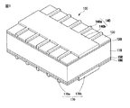
図1は、本発明の実施形態に係る太陽電池の要部斜視図を示したものであり、両面受光型太陽電池の要部斜視図を示したものである。しかし、本発明は前記実施の形態に限定されず、様々な構造の太陽電池に適用が可能である。 FIG. 1 shows a perspective view of relevant parts of a solar cell according to an embodiment of the present invention, and shows a perspective view of relevant parts of a double-sided light receiving solar cell. However, the present invention is not limited to the above embodiment, and can be applied to solar cells having various structures.
両面受光型太陽電池100を有する両面受光型太陽電池モジュールは、隣接する両面受光型太陽電池100を電気的に接続するインターコネクタ、両面受光型太陽電池100を保護する保護膜(EVA:Ethylene Vinyl Acetate)、両面受光型太陽電池100の前面(front surface)の方向に保護膜の上に配置される光透過性の前面基板、及び両面受光型太陽電池100の後面(back surface)の方向に保護膜の後面に配置される光透過性の後面基板を含む。
The double-sided light-receiving solar cell module having the double-sided light-receiving
光透過性の前面基板と光透過性の後面基板は、両面受光型太陽電池モジュールの外部からの湿気が浸透することを防止して、両面受光型太陽電池100を外部環境から保護する。
The light-transmitting front substrate and the light-transmitting rear substrate prevent moisture from the outside of the double-sided light-receiving solar cell module from permeating and protect the double-sided light-receiving
このような光透過性の前面基板と光透過性の後面基板は透過率が高く、破損防止機能に優れた強化ガラスなどから構成されている。この際、強化ガラスは、鉄成分の含有量が低い低鉄分強化ガラス(low iron tempered glass)で有り得る。 Such a light-transmitting front substrate and a light-transmitting rear substrate are made of tempered glass having a high transmittance and an excellent damage prevention function. At this time, the tempered glass may be a low iron tempered glass having a low iron content.
このような光透過性の前面基板と光透過性の後面基板は、光の散乱効果を高めるために内側面がエンボス加工(embossing)処理することができる。 The light-transmitting front substrate and the light-transmitting rear substrate can be embossed on the inner surface to enhance the light scattering effect.
光透過性の前面基板と光透過性の後面基板は、低鉄分強化ガラス(low iron tempered glass)または高分子樹脂から構成することができる。ここで、高分子樹脂としては、ポリエチレンテレフタレート(Poly Ethylene Terephthlate、PET)を使用することができる。 The light-transmitting front substrate and the light-transmitting rear substrate can be composed of low iron tempered glass or polymer resin. Here, polyethylene terephthalate (Poly Ethylene Terephthlate, PET) can be used as the polymer resin.
保護膜は、両面受光型太陽電池100の前面と後面にそれぞれ配置された状態でラミネート工程により、両面受光型太陽電池100と一体化されたもので、水分の浸透による腐食を防止し、両面受光型太陽電池100を衝撃から保護する。
The protective film is integrated with the double-sided light-receiving
このような保護膜は、エチレン酢酸ビニル(EVA、ethylene vinyl acetate)またはシリコン樹脂(silicone resin)からなることができる。しかし、他の物質も使用可能である。 Such a protective film may be made of ethylene vinyl acetate (EVA) or silicon resin. However, other materials can be used.
本実施の形態の両面受光型太陽電池100は、図1に示すように、第1導電型を有する基板110と、基板110の第1面、例えば前面(front surface)に位置し、第1導電型の反対である第2導電型の不純物を含有する第1ドーピング部120、第1ドーピング部120の上に位置し、第1ドーピング部120と電気的及び/または物理的に接続された第1電極部140と、基板110の第2面、例えば後面(back surface)に位置し、第1導電型の不純物を基板110に比べて高濃度で含有する第2ドーピング部150、第2ドーピング部150の後面に位置し、第2ドーピング部150と電気的及び/または物理的に接続された第2電極部170を含む。
As shown in FIG. 1, the double-sided light receiving
基板110は、n型導電型のシリコンウエハからなることができる。この時、シリコンは、単結晶シリコン、多結晶シリコン基板または非晶質シリコンで有り得る。
The
基板110がn型の導電型を有する場合、基板110は、リン(P )、ヒ素(As)、アンチモン(Sb)などのように5が元素の不純物を含有する。
In the case where the
これとは別に、基板110は、p型導電型のシリコンウエハからなることができ、この場合、基板110は、ホウ素(B)、ガリウム(Ga)、インジウム(In)などのような3が元素の不純物を含む。
Alternatively, the
このように、基板110は、n型またはp型の導電型であることがあるが、以下では、基板110がn型の導電型を有するN型基板である場合について説明する。
As described above, the
基板110の前面(front surface)に位置する第1ドーピング部120は基板110の導電型と反対であるp型の導電型を有する不純物部として、基板110とp−n接合を形成する。したがって、本実施の形態では、第1ドーピング部120は、エミッタ部を形成する。
The
基板110が、N型基板である場合、第1ドーピング部120は、p型導電型を有する不純物、例えば、ホウ素(B)、ガリウム(Ga)、インジウム(In)などのような3が元素の不純物を基板110の第1面に均一なドーピング濃度にドーピングすることによって形成することができる。したがって、本実施の形態で、第1ドーピング部120の不純物ドーピング濃度は均一に形成される。
In the case where the
これとは別に、基板110がP型基板である場合、第1ドーピング部120は、n型導電型を有する不純物を基板110の第1面に均一なドーピング濃度でドーピングすることに沿って形成することができる。
In addition, when the
しかし、第1ドーピング部120は、位置に応じて、不純物ドーピング濃度が異なる選択的エミッタ部で構成することができる。
However, the
この場合、第1ドーピング部120は、第1面に位置する第1電極部が形成される位置の不純物ドーピング濃度が第1電極部が形成されない位置の不純物ドーピング濃度が互いに別に形成されることできる。一例として、第1ドーピング部120において、第1電極部が形成される位置の不純物ドーピング濃度は、第1電極部が形成されない位置の不純物ドーピング濃度より高くかまたは低く形成することができる。
In this case, in the
p−n接合に起因する内部の電位差(built-in potential difference)により、基板110に入射された光によって生成された電荷である電子−正孔対は、電子と正孔に分離され、電子はn型の方向に移動し、正孔はp型方向に移動する。
Due to the built-in potential difference caused by the pn junction, the electron-hole pair, which is the charge generated by the light incident on the
したがって、分離された電子は、N型基板110の方向に移動し、分離された正孔は、第1ドーピング部120の方向にに移動する。したがって、N型基板110では、電子が複数キャリアとなり、第1ドーピング部120では正孔が複数キャリアになる。
Accordingly, the separated electrons move in the direction of the N-
第1ドーピング部120の上に前面誘電層130が形成されることができる。前面誘電層130は、金属酸化物(metal oxide)系列の物質、例えばシリコン窒化膜(SiNx)、シリコン酸化膜(SiOx)、酸化アルミニウム膜(AlOx)及び二酸化チタン膜(TiO2)の中から選ばれた少なくとも一つの膜に形成されることができ、基板110の前面(front surface)を介して入射される光の反射率を減らし、特定の波長領域の選択性を増加させる反射防止膜として機能することができる。また、前面誘電層130は、パッシベーション膜としても機能することもできる。しかし、前面誘電層130は、基板110の第1面に形成されないこともある。
A
基板110の前面(front surface)に位置する場合、前面誘電層130は、第1ドーピング部120の一部を露出する開口部を含むことができ、開口部によって露出された第1ドーピング部120上には第1電極部140が形成される。
When located on the front surface of the
第1電極部140は、第1方向(X−X’)に延長された複数のフィンガー電極140aと、第1方向と直交する第2方向(Y−Y’)に延長された複数のバスバー電極140bを含むことができる。
The
このような構成の第1電極部140は、電気伝導度を確保するための第1導電性粒子(P1)、及び第1導電性粒子(P1)に比べて高い仕事関数を有する第2導電性粒子(P2)を含む。
The
第1導電性粒子(P1)は、電気伝導度が優れた金属、例えば、銀(Ag)からなり得、第2導電性粒子(P2)は、第1ドーピング部120と接触する界面にシリサイド(NS)を形成することができる金属、例えば、ニッケル(Ni)から成り得る。
The first conductive particles (P1) may be made of a metal having excellent electrical conductivity, for example, silver (Ag), and the second conductive particles (P2) may be silicided at the interface contacting the
第2導電性粒子(P2)がニッケルからなる場合、第2導電性粒子(P2)と第1ドーピング部120の界面には、ニッケルシリサイド(Ni silicide)(NS)が形成される。第1電極部140は基板110の第1導電性粒子(P1)と第2導電性粒子(P2)の接着性を確保するための樹脂(resin)(R)をさらに含む。
When the second conductive particles (P2) are made of nickel, nickel silicide (NS) is formed at the interface between the second conductive particles (P2) and the
第1電極部140の樹脂(R)は、モノマー(monomer)系のエポキシ(epoxy)樹脂またはアクリル(acrylic)樹脂を含む熱硬化性樹脂から形成することができる。
The resin (R) of the
このような構成の第1電極部140は、樹脂(R)、樹脂(R)内に分散された第1導電性粒子(P1)及び第2導電性粒子(P2)を含む電極ペーストを印刷、乾燥、硬化及びシリサイド化(silicidation)することによって形成される。
The
前述のように、第1電極部140は、銀(Ag)から形成された第1導電性粒子(P1)とニッケル(Ni)から形成された第2導電性粒子(P2)を含み、第2導電性粒子(P2)と第1ドーピング部120の界面には、ニッケルシリサイド(NS)が位置する。
As described above, the
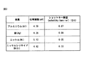
ところで、図3に示すように、第2導電性粒子(P2)を構成するニッケル(Ni)は、第1導電性粒子(P1)を構成する銀(Ag)に比べて高い仕事関数を有する。 Incidentally, as shown in FIG. 3, nickel (Ni) constituting the second conductive particles (P2) has a higher work function than silver (Ag) constituting the first conductive particles (P1).
図3を参照すると、銀(Ag)は、約4.26eVの仕事関数を有するが、ニッケル(Ni)は、銀(Ag)に比べて高い約5.10eVの仕事関数を有することがわかる。また、図3を参照すると、N型基板110が多結晶シリコンから形成された場合には、銀(Ag)のショットキー障壁は約0.89であるが、ニッケル(Ni)のショットキー障壁は、銀(Ag)に比べて非常に低い約0.05であることがわかる。
Referring to FIG. 3, it can be seen that silver (Ag) has a work function of about 4.26 eV, while nickel (Ni) has a higher work function of about 5.10 eV than silver (Ag). Referring to FIG. 3, when the N-
したがって、第1導電性粒子(P1)に比べて高い仕事関数を有する第2導電性粒子(P2)を含む第1電極部140は、第1導電性粒子(P1)と第2導電性粒子(P2)の内、第1導電性粒子(P1)のみ含む場合に比べて、第1電極部140と第1ドーピング部120の接触抵抗が減少する。
Accordingly, the
また、第2導電性粒子(P2)と第1ドーピング部120の界面に位置するニッケルシリサイド(NS)は、約4.82eVの仕事関数を有し、約0.33のショットキー障壁を有するので、ニッケルシリサイド(NS)は、ニッケル(Ni)に比べては仕事関数が低く、ショットキー障壁が高いが、ニッケル(Ni)に比べて低い比抵抗(specific resistance)を有する。
Further, nickel silicide (NS) located at the interface between the second conductive particles (P2) and the
したがって、第2導電性粒子(P2)と第1ドーピング部120の界面に位置するニッケルシリサイド(NS)により、第1電極部140と第1ドーピング部120の接触抵抗がさらに減少する。
Therefore, the contact resistance between the
図4を参照すると、第1導電性粒子と、第2導電性粒子の内、第1導電性粒子のみ含む従来の場合、ショットキー障壁は、第1高さ(Φb1)を有するが、第1導電性粒子と、第2導電性粒子とニッケルシリサイドを有する本発明の場合、ショットキー障壁は、第1高さ(Φb1)に比べて一定の高さ(ΔΦb)ほど減少する、第2高さ(Φb2)を有することがわかる。 Referring to FIG. 4, the Schottky barrier has a first height (Φb1) in the conventional case including only the first conductive particles among the first conductive particles and the second conductive particles. In the case of the present invention having conductive particles, second conductive particles and nickel silicide, the Schottky barrier decreases by a certain height (ΔΦb) compared to the first height (Φb1), the second height. It can be seen that it has (Φb2).
本発明の実施の形態において、第1導電性粒子(P1)が、銀(Ag)から構成され、第2導電性粒子(P2)がニッケルから構成された場合、ニッケル(P2)は、銀(P1)とニッケル(P2)を合わせた全重量に対して15重量%〜25重量%程度含有されることが望ましい。 In the embodiment of the present invention, when the first conductive particles (P1) are composed of silver (Ag) and the second conductive particles (P2) are composed of nickel, nickel (P2) is silver ( It is desirable to contain about 15 wt% to 25 wt% with respect to the total weight of P1) and nickel (P2).
ニッケル(P2)は、銀(P1)に比べて約5倍程度の高い比抵抗を有するので。熱硬化性樹脂内に分散される導電性粒子として、銀(P1)及びニッケル(P2)を一緒に使用しないでニッケル(P2)のみを使用する場合には、第1電極部140のライン(line)抵抗が非常に大きくて太陽電池の電気的特性が低いという問題点がある。 Nickel (P2) has a specific resistance about five times higher than silver (P1). When only nickel (P2) is used as the conductive particles dispersed in the thermosetting resin without using silver (P1) and nickel (P2) together, the line of the first electrode part 140 (line) ) There is a problem that the resistance is very large and the electrical characteristics of the solar cell are low.
また、銀(P1)とニッケル(P2)を一緒に使用してもニッケル(P2)の含有量が増加するほど、第1電極部140のライン抵抗が増加する。
Even if silver (P1) and nickel (P2) are used together, the line resistance of the
したがって、銀(P1)とニッケル(P2)を合わせた全重量のニッケル(P2)の含有量は、第1電極部140のライン抵抗と、第1電極部140と第1ドーピング部120の接触抵抗を一緒に考慮して設定することが望ましい。
Accordingly, the total content of nickel (P2) including silver (P1) and nickel (P2) includes the line resistance of the
本発明の実験によると、銀(P1)とニッケル(P2)を合わせた全重量に対してニッケル(P2)の含有量が25重量%以上である場合には、ニッケル含有量がさらに増加しても、太陽電池の電気的特性がこれ以上は改善されないことがわかった。 According to the experiment of the present invention, when the content of nickel (P2) is 25% by weight or more based on the total weight of silver (P1) and nickel (P2), the nickel content is further increased. However, it was found that the electrical characteristics of the solar cell are not improved further.
また、ニッケルの含有量が15重量%未満の場合には、ショットキー障壁の高さを効果的に下げることができず、ニッケルシリサイド(NS)の生成量がわずかであるので、第1ドーピング部と、第1電極部との間の接触抵抗の改善効果も微々たるものことがわかった。 In addition, when the nickel content is less than 15% by weight, the height of the Schottky barrier cannot be effectively reduced, and the amount of nickel silicide (NS) generated is small. It was also found that the effect of improving the contact resistance between the first electrode part and the first electrode part was slight.
したがって、銀(P1)とニッケル(P2)を合わせた全重量に対してニッケル(P2)の含有量は15重量%〜25重量%であることが望ましい。 Therefore, the content of nickel (P2) is preferably 15% by weight to 25% by weight with respect to the total weight of silver (P1) and nickel (P2).
一方、ニッケル(P2)の大きさ(size)が小さすぎる場合、例えば、ニッケル(P2)が、ナノ(nano)単位の大きさを有する場合には、ニッケル(P2)を樹脂(R)内に効果的に分散させることが難しく、分散安定剤のような添加物を使用するが、前記添加物は、ライン抵抗を増加させる。 On the other hand, when the size of nickel (P2) is too small, for example, when nickel (P2) has a size of nano (nano) unit, nickel (P2) is placed in the resin (R). Difficult to disperse effectively and uses additives such as dispersion stabilizers, which increase line resistance.
ここで、ニッケル(P2)の大きさは、粒径(diameter)で有り得る。 Here, the size of nickel (P2) may be a particle size.
したがって、本発明の実施の形態では、分散安定剤のような添加物を使用しなくてもニッケル(P2)を樹脂(R)内に効果的に分散させるために、マイクロ(micro)単位の大きさを有するニッケル(P2)を使用する。 Therefore, in the embodiment of the present invention, in order to effectively disperse nickel (P2) in the resin (R) without using an additive such as a dispersion stabilizer, the size of the micro unit is small. Nickel (P2) having a thickness is used.
一例として、ニッケル(P2)は、2μm〜10μmの大きさを有することが望ましい。 As an example, nickel (P2) desirably has a size of 2 μm to 10 μm.
このような構成の第1電極部140は、第1ドーピング部120の方向に移動した電荷、例えば正孔を収集する。
The
基板110の後面に位置する第2電極部170は基板110の方向に移動する電荷、例えば、電子を収集して外部装置に出力する。
The
本実施の形態で、第2電極部170は、第1電極部140のバスバー電極140bに対 応する位置に形成されるバスバー電極170bと、第1電極部140のフィンガー電極140aに対応する位置に形成されるフィンガー電極170aを含む。
In the present embodiment, the
このとき、第2電極部170のフィンガー電極170aは、第1電極部140のフィンガー電極140aに比べて多い個数で形成されることが望ましい。
At this time, the
第2電極部170は、第1電極部140を形成する電極ペーストにより構成することができる。この場合、第2電極部は、第1導電性粒子(P1)と第2導電性粒子(P2)が樹脂(R)内に分散された電極ペーストを印刷、乾燥及び硬化することにより形成することができる。
The
第2電極部170が電気的及び/または物理的に接続される第2ドーピング部150は基板110の後面全体に位置し、基板110との不純物濃度差によって電位障壁を形成することにより、基板110の後面方向への正孔の移動を妨害する後面電界部で作用する。したがって、基板110の表面近辺で電子と正孔が再結合して消滅することが減少される。
The
これとは異なり、第2ドーピング部150は、第2電極部170が位置する領域の基板の後面に局部的に(locally)位置することができ、選択的エミッタ部と同様に、不純物ドーピング濃度が互いに異なる選択的構造で形成することができる。
In contrast, the
選択的構造を有する後面電界部の場合、第2電極部170が位置する領域の不純物ドーピング濃度は、第2電極部170が位置しない領域の不純物ドーピング濃度より高いか低いことがある。
In the case of the rear surface electric field portion having a selective structure, the impurity doping concentration in the region where the
第2電極部170が第1電極部140を形成する電極ペーストと同じ構成の電極ペーストにより形成される場合には、第1電極部140と同一または類似の方法で、第2ドーピング部150と第2導電性粒子(P2)の界面にシリサイドが形成される。
When the
この場合、図2に示した第1ドーピング部120は、第2ドーピング部150であり得、前面誘電層130は、第2電極部170が位置しない第2ドーピング部150の後面に位置する後面誘電層160で有り得る。
In this case, the
後面誘電層160は、前面誘電層130のように、シリコン窒化膜(SiNx)、シリコン酸化膜(SiOx)、酸化アルミニウム膜(AlOx)及び二酸化チタン膜(TiO2 )の中から選ばれた少なくとも一つの膜から形成されることができ、前面誘電層130と同様に、必要に応じて序魚除去されることができる。
Like the
このような構成の両面受光型太陽電池において、太陽電池に照射された光が第1ドーピング部120及び第2ドーピング部150を介して基板110に入射されると、基板110に入射された光のエネルギーによって電子‐正孔対が発生する。
In the double-sided light receiving solar cell having such a configuration, when light irradiated to the solar cell is incident on the
基板の前面(front surface)に前面誘電そう130が位置し、基板の後面(back surface)に後面誘電層160が位置する場合、前面誘電層130と後面誘電層160によって基板110に入射される光の反射損失が減少して基板110に入射される光の量はさらに増加する。
When the
これらの電子−正孔対は、基板110と第1ドーピング部120のp−n接合によって互いに分離され、前者はn型の導電型を有する基板110方向に移動し、正孔はp型の導電型を有する第1ドーピング部120方向に移動する。
These electron-hole pairs are separated from each other by the pn junction of the
このように、基板110方向に移動した電子は、第2ドーピング部150を介して第2電極部170に移動し、第1ドーピング部120方向にに移動した正孔は、第1電極部140に移動する。
As described above, the electrons moved in the direction of the
したがって、いずれかの1つ太陽電池の第1電極部140と、隣接する太陽電池の第2電極部170をインターコネクタなどの導体に接続すると、電流が流れるようになり、これを外部で電力として利用することになる。
Therefore, when the
以下、太陽電池の製造方法について説明する。図5は図1に示した太陽電池の製造方法を示す工程ブロック図である。 Hereinafter, the manufacturing method of a solar cell is demonstrated. FIG. 5 is a process block diagram showing a method for manufacturing the solar cell shown in FIG.
本発明の実施形態に係る太陽電池を製造するために、まず、第1導電型の基板、例えば、N型基板110の第1面に第1導電型と反対の第2導電型の不純物を含有する第1ドーピング部120を形成する。
In order to manufacture a solar cell according to an embodiment of the present invention, first, a first conductivity type substrate, for example, a first surface of an N-
第1ドーピング部120を形成する前に、基板110の第1面は、テクスチャリング処理されることができ、テクスチャリング処理された基板110の第1面には複数の凹凸が形成されることができる。
Prior to forming the
続いて、第1ドーピング部120の上に前面誘電層130を形成する。前面誘電層130は、CVD(chemical vapor deposition)またはPECVD(plasma enhanced chemical vapor deposition)工程から形成することができ、単層または複数の層から形成することができる。
Subsequently, the
前面誘電層130を形成した後、前面誘電層130を部分的にエッチングして第1電極部140が形成される領域の第1ドーピング部120を露出させる。前面誘電層130を部分的にエッチングすると、前面誘電層130は、第1ドーピング部120の一部を露出する開口部を含み、開口部は、第1電極部140と同じパターン、例えば、グリッド(grid)のパターンに形成することができる。
After the
前面誘電層130に開口部を形成する際にレーザーを使用することができるが、これに限定するものではなく、通常の写真工程(photolithography)を使用することもできる。
A laser may be used to form the opening in the
次に、開口部を介して露出された第1ドーピング部120の上に低温硬化型電極ペーストを印刷及び乾燥する。
Next, a low-temperature curable electrode paste is printed and dried on the
以上では、前面誘電層130を形成した後、電極ペーストを印刷及び乾燥する場合について説明したが、第1ドーピング部120の上に前面誘電層130を形成せずに電極ペーストを印刷、乾燥することも可能である。
In the above description, the electrode paste is printed and dried after the
低温硬化型電極ペーストは、熱硬化性樹脂(R)、熱硬化性樹脂内に分散された第1導電性粒子(P1)と、熱硬化性樹脂(R)内に分散され、第1導電性粒子(P1)に比べて高い仕事関数を有し、第1ドーピング部120と接触する界面にシリサイド(NS)を形成する第2導電性粒子(P2)を含む。
The low temperature curable electrode paste includes the thermosetting resin (R), the first conductive particles (P1) dispersed in the thermosetting resin, and the first conductive particles dispersed in the thermosetting resin (R). Second conductive particles (P2) having a work function higher than that of the particles (P1) and forming silicide (NS) at the interface contacting the
ここで、熱硬化性樹脂(R)は、低温(例えば、230℃〜260℃)で熱処理され硬化する特性を有するモノマー系のエポキシ(epoxy)樹脂またはアクリル(acrylic)樹脂を含むことことができる。そして、第1導電性粒子(P1)は、銀(Ag)であり得、第2導電性粒子(P2)は、ニッケル(Ni)で有り得る。 Here, the thermosetting resin (R) may include a monomer-based epoxy resin or acrylic resin having a property of being cured by heat treatment at a low temperature (for example, 230 ° C. to 260 ° C.). . The first conductive particles (P1) may be silver (Ag), and the second conductive particles (P2) may be nickel (Ni).
低温硬化型電極ペーストを乾燥した後、約240℃の低温で熱処理を行い、電極ペーストを硬化させる。 After drying the low temperature curable electrode paste, heat treatment is performed at a low temperature of about 240 ° C. to cure the electrode paste.
グラスフリットとグラスフリット内に分散された第1導電性粒子(Ag)を含む従来の電極ペーストを硬化させるためには、本発明の実施の形態に係る低温硬化型電極ペーストに比べて高い温度(例えば、800℃〜900℃)で熱処理を実施しなければならない。 In order to cure the conventional electrode paste including the glass frit and the first conductive particles (Ag) dispersed in the glass frit, a temperature higher than that of the low-temperature curable electrode paste according to the embodiment of the present invention ( For example, heat treatment must be performed at 800 ° C. to 900 ° C.).
しかし、本発明の電極ペーストは、エッチング成分を含むガラスフリットを備えておらず、グラスフリットの代わりに低温(例えば、230℃〜260℃)で硬化する熱硬化性樹脂(R)を含むため、第1ドーピング部120と基板110に加わる熱損傷を最小限に抑えることができ、基板110を構成するシリコンバルクの寿命が増加し、開放電圧と短絡電流密度が向上するため、太陽電池の効率を向上させることができる。
However, the electrode paste of the present invention does not include a glass frit containing an etching component, and includes a thermosetting resin (R) that cures at a low temperature (for example, 230 ° C. to 260 ° C.) instead of the glass frit. The thermal damage applied to the
230℃〜260℃の低温工程で低温硬化型電極ペーストを硬化した後、不活性ガス雰囲気中で約350℃〜400℃の温度で基板110を加熱して、第2導電性粒子と、第1ドーピング部120が接する界面にシリサイド(NS)を形成する。
After curing the low temperature curable electrode paste in a low temperature process of 230 ° C. to 260 ° C., the
本発明の実施の形態では、第2導電性粒子(P2)がニッケルである場合を例に挙げて説明したので、第1ドーピング部120と接する界面には、ニッケルシリサイド(NS)が形成される。
In the embodiment of the present invention, since the case where the second conductive particles (P2) are nickel has been described as an example, nickel silicide (NS) is formed at the interface in contact with the
一方、両面受光型太陽電池の場合、基板の第1面には、第1ドーピング部を形成する基板の第2面には、第2ドーピング部を形成する段階と、基板の第1面には、前面誘電層を形成し、基板の第2面には、後面誘電層を形成する段階と、前面誘電層と後面誘電層にそれぞれ開口部を形成する段階と、前面誘電層に形成された開口部を介して露出された第1ドーピング部には、前面電極部を形成するための電極ペーストを塗布し、後面誘電層に形成された開口部を介して露出された第2ドーピング部には、後面電極部を形成するための電極ペーストを塗布する段階と、それぞれの電極ペーストを低温工程で熱処理して硬化する段階と、シリサイドを形成する段階に応じて、太陽電池を製造することができる。 On the other hand, in the case of a double-sided light receiving solar cell, on the first surface of the substrate, a second doping portion is formed on the second surface of the substrate on which the first doping portion is formed; Forming a front dielectric layer, forming a rear dielectric layer on the second surface of the substrate, forming openings in the front dielectric layer and the rear dielectric layer, and an opening formed in the front dielectric layer; The first doping part exposed through the part is coated with an electrode paste for forming the front electrode part, and the second doping part exposed through the opening formed in the rear dielectric layer has A solar cell can be manufactured according to the step of applying an electrode paste for forming the rear electrode portion, the step of curing each electrode paste by heat treatment in a low-temperature process, and the step of forming silicide.
Claims (18)
前記基板の第1面に位置し、第1導電型とは異なる第2導電型の不純物を含有する第1ドーピング部と、
前記第1ドーピング部と電気的に接続された第1電極部と
を含み、
前記第1電極部は、熱硬化性樹脂と、前記熱硬化性樹脂内に分散された第1導電性粒子と、第2導電性粒子と、前記第2導電性粒子と前記第1ドーピング部の接触界面に位置するシリサイドを含み、
前記第1導電性粒子は銀(Ag)から構成され、前記第2導電性粒子は前記第1導電性粒子と比べて高い仕事関数を有するニッケル(Ni)から構成され、
前記ニッケルは、銀とニッケルを合せた全重量に対して15重量%〜25重量%の割合で含有される、太陽電池。 A first conductivity type substrate;
A first doping part located on the first surface of the substrate and containing an impurity of a second conductivity type different from the first conductivity type;
A first electrode part electrically connected to the first doping part;
The first electrode unit includes a thermosetting resin, first conductive particles dispersed in the thermosetting resin, second conductive particles, the second conductive particles, and the first doping unit. Including silicide located at the contact interface;
The first conductive particles are composed of silver (Ag), and the second conductive particles are composed of nickel (Ni) having a higher work function than the first conductive particles,
The said nickel is a solar cell contained in the ratio of 15 to 25 weight% with respect to the total weight which combined silver and nickel.
2μm〜10μmの大きさを有する、請求項1記載の太陽電池。 The nickel is
The solar cell of Claim 1 which has a magnitude | size of 2 micrometers-10 micrometers.
モノマー系のエポキシ樹脂またはアクリル樹脂を含む、請求項1記載の太陽電池。 The thermosetting resin is
The solar cell of Claim 1 containing a monomer-type epoxy resin or an acrylic resin.
エミッタ部から形成される、請求項1記載の太陽電池。 The first doping unit includes
The solar cell according to claim 1, wherein the solar cell is formed from an emitter portion.
前記第2ドーピング部と電気的に接続された第2電極部と
をさらに含み、
前記第2電極部は、前記第1導電性粒子、前記第2導電性粒子、前記シリサイド及び前記熱硬化性樹脂を含む、請求項1記載の太陽電池。 A second doping part located on a second surface opposite to the first surface of the substrate and containing the impurity of the first conductivity type at a higher concentration than the substrate;
A second electrode part electrically connected to the second doping part;
The solar cell according to claim 1, wherein the second electrode portion includes the first conductive particles, the second conductive particles, the silicide, and the thermosetting resin.
前記第1ドーピング部の一部を露出する開口部を備える誘電層を前記第1ドーピング部上に形成する段階と、
前記第1ドーピング部と電気的に接続された第1電極部を形成する段階と、を含み、
前記第1電極部を形成する段階は、
熱硬化性樹脂、前記熱硬化性樹脂内に分散された第1導電性粒子と、前記熱硬化性樹脂内に分散され、前記第1導電性粒子に比べて高い仕事関数を有する第2導電性粒子を含む電極ペーストを前記開口部を介して露出された前記第1ドーピング部に印刷する段階と、
前記電極ペーストを熱処理して硬化する段階と、
前記第2導電性粒子と、前記第1ドーピング部が接触する界面にシリサイドを形成する段階と
を含み、
前記第1電極部は、熱硬化性樹脂と、前記熱硬化性樹脂内に分散された第1導電性粒子と、第2導電性粒子と、前記第2導電性粒子と第1ドーピング部の接触界面に位置するシリサイドを含み、
前記第1導電性粒子は銀(Ag)から構成され、前記第2導電性粒子は前記第1導電性粒子と比べて高い仕事関数を有するニッケル(Ni)から構成され、
前記ニッケルは、銀とニッケルを合せた全重量に対して15重量%〜25重量%の割合で含有される、太陽電池の製造方法。 Forming a first doping portion containing an impurity of a second conductivity type different from the first conductivity type on a first surface of a substrate having the first conductivity type;
Forming a dielectric layer having an opening exposing a portion of the first doping portion on the first doping portion;
Forming a first electrode part electrically connected to the first doping part ,
The step of forming the first electrode part includes :
Thermosetting resin, first conductive particles dispersed in the thermosetting resin, and second conductivity dispersed in the thermosetting resin and having a higher work function than the first conductive particles. Printing an electrode paste including particles on the first doping part exposed through the opening;
Curing the electrode paste by heat treatment;
Forming a silicide at an interface with which the second conductive particles and the first doping part are in contact;
The first electrode unit includes a thermosetting resin, first conductive particles dispersed in the thermosetting resin, second conductive particles, and contact between the second conductive particles and the first doping unit. Including silicide located at the interface;
The first conductive particles are composed of silver (Ag), and the second conductive particles are composed of nickel (Ni) having a higher work function than the first conductive particles,
The said nickel is a manufacturing method of a solar cell contained in the ratio of 15 to 25 weight% with respect to the total weight which combined silver and nickel.
Applications Claiming Priority (2)
| Application Number | Priority Date | Filing Date | Title |
|---|---|---|---|
| KR1020130056314A KR101614186B1 (en) | 2013-05-20 | 2013-05-20 | Solar cell and manufacturing method thereof |
| KR10-2013-0056314 | 2013-05-20 |
Publications (2)
| Publication Number | Publication Date |
|---|---|
| JP2014229904A JP2014229904A (en) | 2014-12-08 |
| JP5952336B2 true JP5952336B2 (en) | 2016-07-13 |
Family
ID=50390981
Family Applications (1)
| Application Number | Title | Priority Date | Filing Date |
|---|---|---|---|
| JP2014103448A Active JP5952336B2 (en) | 2013-05-20 | 2014-05-19 | Solar cell and manufacturing method thereof |
Country Status (5)
| Country | Link |
|---|---|
| US (1) | US11004988B2 (en) |
| EP (1) | EP2806465B1 (en) |
| JP (1) | JP5952336B2 (en) |
| KR (1) | KR101614186B1 (en) |
| CN (1) | CN104183656B (en) |
Families Citing this family (4)
| Publication number | Priority date | Publication date | Assignee | Title |
|---|---|---|---|---|
| DE202015102238U1 (en) * | 2015-05-04 | 2015-06-01 | Solarworld Innovations Gmbh | Photovoltaic cell and photovoltaic module |
| CN116647680A (en) | 2016-10-28 | 2023-08-25 | 韩国电子通信研究院 | Video encoding/decoding method and apparatus, and recording medium storing bit stream |
| KR101980946B1 (en) * | 2016-11-11 | 2019-05-21 | 삼성에스디아이 주식회사 | Front electrode for solar cell and solar cell comprising the same |
| KR20210103850A (en) * | 2020-02-14 | 2021-08-24 | 엘지전자 주식회사 | Solar cell, and solar cell panel and method of manufacturing the same |
Family Cites Families (21)
| Publication number | Priority date | Publication date | Assignee | Title |
|---|---|---|---|---|
| JPS5896777A (en) | 1981-12-03 | 1983-06-08 | Mitsubishi Electric Corp | Solar battery |
| JP3254044B2 (en) | 1993-06-16 | 2002-02-04 | ナミックス株式会社 | Electrodes for solar cells |
| JP3557148B2 (en) | 2000-02-21 | 2004-08-25 | 三洋電機株式会社 | Solar cell module |
| US8575474B2 (en) | 2006-03-20 | 2013-11-05 | Heracus Precious Metals North America Conshohocken LLC | Solar cell contacts containing aluminum and at least one of boron, titanium, nickel, tin, silver, gallium, zinc, indium and copper |
| JP2008135654A (en) | 2006-11-29 | 2008-06-12 | Sanyo Electric Co Ltd | Solar battery module |
| TWI330998B (en) * | 2007-01-16 | 2010-09-21 | Chimei Innolux Corp | Top emitter organic electroluminescent display |
| JP4992449B2 (en) * | 2007-02-06 | 2012-08-08 | 株式会社村田製作所 | Thick film conductor composition and solar cell back Ag electrode |
| US20100037941A1 (en) * | 2008-08-13 | 2010-02-18 | E. I. Du Pont De Nemours And Company | Compositions and processes for forming photovoltaic devices |
| CN101752452A (en) * | 2008-12-01 | 2010-06-23 | 台湾茂矽电子股份有限公司 | Method for manufacturing double-sided solar battery |
| US8710355B2 (en) | 2008-12-22 | 2014-04-29 | E I Du Pont De Nemours And Company | Compositions and processes for forming photovoltaic devices |
| JP2010182935A (en) * | 2009-02-06 | 2010-08-19 | Sharp Corp | Method of manufacturing thin film solar cell |
| JP5144857B2 (en) | 2010-03-01 | 2013-02-13 | 株式会社ノリタケカンパニーリミテド | Conductive paste composition for solar cell |
| TWI475702B (en) | 2010-07-09 | 2015-03-01 | Sakamoto Jun | A panel, a panel manufacturing method, a solar cell module, a printing apparatus, and a printing method |
| US20120037216A1 (en) | 2010-08-13 | 2012-02-16 | Samsung Electronics Co., Ltd. | Conductive paste and electronic device and solar cell including an electrode formed using the conductive paste |
| KR101665722B1 (en) | 2010-09-27 | 2016-10-24 | 엘지전자 주식회사 | Solar cell and manufacturing method thereof |
| US20120142140A1 (en) * | 2010-12-02 | 2012-06-07 | Applied Nanotech Holdings, Inc. | Nanoparticle inks for solar cells |
| KR20120079591A (en) | 2011-01-05 | 2012-07-13 | 엘지전자 주식회사 | Solar cell and manufacturing method thereof |
| KR20120091629A (en) * | 2011-02-09 | 2012-08-20 | 엘지전자 주식회사 | Solar cell |
| DE102011016335B4 (en) * | 2011-04-07 | 2013-10-02 | Universität Konstanz | Nickel-containing and corrosive printable paste and method for forming electrical contacts in the manufacture of a solar cell |
| US8901414B2 (en) * | 2011-09-14 | 2014-12-02 | International Business Machines Corporation | Photovoltaic cells with copper grid |
| WO2013106225A1 (en) * | 2012-01-12 | 2013-07-18 | Applied Materials, Inc. | Methods of manufacturing solar cell devices |
-
2013
- 2013-05-20 KR KR1020130056314A patent/KR101614186B1/en active IP Right Grant
-
2014
- 2014-03-20 US US14/221,111 patent/US11004988B2/en active Active
- 2014-03-28 EP EP14001166.9A patent/EP2806465B1/en active Active
- 2014-05-19 JP JP2014103448A patent/JP5952336B2/en active Active
- 2014-05-20 CN CN201410214046.3A patent/CN104183656B/en active Active
Also Published As
| Publication number | Publication date |
|---|---|
| EP2806465A3 (en) | 2015-04-01 |
| KR101614186B1 (en) | 2016-04-20 |
| CN104183656A (en) | 2014-12-03 |
| US20140338738A1 (en) | 2014-11-20 |
| CN104183656B (en) | 2017-01-18 |
| EP2806465B1 (en) | 2017-01-04 |
| KR20140136562A (en) | 2014-12-01 |
| JP2014229904A (en) | 2014-12-08 |
| EP2806465A2 (en) | 2014-11-26 |
| US11004988B2 (en) | 2021-05-11 |
Similar Documents
| Publication | Publication Date | Title |
|---|---|---|
| JP5302414B2 (en) | Solar cell and manufacturing method thereof | |
| TWI662715B (en) | Solar cell | |
| US8039292B2 (en) | Holey electrode grids for photovoltaic cells with subwavelength and superwavelength feature sizes | |
| WO2017002927A1 (en) | Solar battery and solar battery module | |
| EP2458649B1 (en) | Solar cell | |
| US9337357B2 (en) | Bifacial solar cell module | |
| JP5746263B2 (en) | Solar cell and manufacturing method thereof | |
| EP2538447B1 (en) | Solar cell and method for manufacturing the same | |
| JP5952336B2 (en) | Solar cell and manufacturing method thereof | |
| US20120055538A1 (en) | Solar cell module | |
| US8536447B2 (en) | Electrode of solar cell and fabricating method thereof | |
| JP6810708B2 (en) | Back contact type photovoltaic cell with induced coupling | |
| KR100990108B1 (en) | Solar cell and method for manufacturing the same | |
| US20120192942A1 (en) | Solar cell and method for manufacturing the same | |
| US9929297B2 (en) | Solar cell and method for manufacturing the same | |
| JP2019204870A (en) | Solar cell element and method for manufacturing solar cell element | |
| US9209335B2 (en) | Solar cell system | |
| KR101852237B1 (en) | Perovskite photovoltaic cell module | |
| KR101666748B1 (en) | Perovskite photovoltaic cell module | |
| US9059357B2 (en) | Bifacial solar cell | |
| KR20110045979A (en) | Solar cell and method for manufacturing the same | |
| KR101186242B1 (en) | Optoelectronic component having three-dimentional pattern and fablication method thereof | |
| CN117412617B (en) | Laminated solar cell, manufacturing method thereof, photovoltaic module and photovoltaic system | |
| TWM542861U (en) | Solar cell | |
| TWI733970B (en) | Solar cell and operation method thereof |
Legal Events
| Date | Code | Title | Description |
|---|---|---|---|
| A977 | Report on retrieval |
Free format text: JAPANESE INTERMEDIATE CODE: A971007 Effective date: 20150319 |
|
| A131 | Notification of reasons for refusal |
Free format text: JAPANESE INTERMEDIATE CODE: A131 Effective date: 20150324 |
|
| A521 | Request for written amendment filed |
Free format text: JAPANESE INTERMEDIATE CODE: A523 Effective date: 20150624 |
|
| A131 | Notification of reasons for refusal |
Free format text: JAPANESE INTERMEDIATE CODE: A131 Effective date: 20151110 |
|
| A521 | Request for written amendment filed |
Free format text: JAPANESE INTERMEDIATE CODE: A523 Effective date: 20160108 |
|
| TRDD | Decision of grant or rejection written | ||
| A01 | Written decision to grant a patent or to grant a registration (utility model) |
Free format text: JAPANESE INTERMEDIATE CODE: A01 Effective date: 20160510 |
|
| A61 | First payment of annual fees (during grant procedure) |
Free format text: JAPANESE INTERMEDIATE CODE: A61 Effective date: 20160609 |
|
| R150 | Certificate of patent or registration of utility model |
Ref document number: 5952336 Country of ref document: JP Free format text: JAPANESE INTERMEDIATE CODE: R150 |
|
| R250 | Receipt of annual fees |
Free format text: JAPANESE INTERMEDIATE CODE: R250 |
|
| R250 | Receipt of annual fees |
Free format text: JAPANESE INTERMEDIATE CODE: R250 |
|
| R250 | Receipt of annual fees |
Free format text: JAPANESE INTERMEDIATE CODE: R250 |
|
| R250 | Receipt of annual fees |
Free format text: JAPANESE INTERMEDIATE CODE: R250 |
|
| S111 | Request for change of ownership or part of ownership |
Free format text: JAPANESE INTERMEDIATE CODE: R313113 |
|
| R350 | Written notification of registration of transfer |
Free format text: JAPANESE INTERMEDIATE CODE: R350 |
|
| R250 | Receipt of annual fees |
Free format text: JAPANESE INTERMEDIATE CODE: R250 |
|
| S533 | Written request for registration of change of name |
Free format text: JAPANESE INTERMEDIATE CODE: R313533 |
|
| R350 | Written notification of registration of transfer |
Free format text: JAPANESE INTERMEDIATE CODE: R350 |