JP5952336B2 - 太陽電池及びその製造方法 - Google Patents
太陽電池及びその製造方法 Download PDFInfo
- Publication number
- JP5952336B2 JP5952336B2 JP2014103448A JP2014103448A JP5952336B2 JP 5952336 B2 JP5952336 B2 JP 5952336B2 JP 2014103448 A JP2014103448 A JP 2014103448A JP 2014103448 A JP2014103448 A JP 2014103448A JP 5952336 B2 JP5952336 B2 JP 5952336B2
- Authority
- JP
- Japan
- Prior art keywords
- conductive particles
- solar cell
- doping
- nickel
- electrode
- Prior art date
- Legal status (The legal status is an assumption and is not a legal conclusion. Google has not performed a legal analysis and makes no representation as to the accuracy of the status listed.)
- Active
Links
- 238000004519 manufacturing process Methods 0.000 title claims description 14
- PXHVJJICTQNCMI-UHFFFAOYSA-N Nickel Chemical compound [Ni] PXHVJJICTQNCMI-UHFFFAOYSA-N 0.000 claims description 129
- 239000002245 particle Substances 0.000 claims description 80
- 239000000758 substrate Substances 0.000 claims description 80
- 229910052759 nickel Inorganic materials 0.000 claims description 48
- BQCADISMDOOEFD-UHFFFAOYSA-N Silver Chemical compound [Ag] BQCADISMDOOEFD-UHFFFAOYSA-N 0.000 claims description 36
- 229910052709 silver Inorganic materials 0.000 claims description 31
- 239000004332 silver Substances 0.000 claims description 31
- 229920005989 resin Polymers 0.000 claims description 29
- 239000011347 resin Substances 0.000 claims description 29
- RUFLMLWJRZAWLJ-UHFFFAOYSA-N nickel silicide Chemical compound [Ni]=[Si]=[Ni] RUFLMLWJRZAWLJ-UHFFFAOYSA-N 0.000 claims description 27
- 229910021334 nickel silicide Inorganic materials 0.000 claims description 27
- 239000002003 electrode paste Substances 0.000 claims description 23
- 239000012535 impurity Substances 0.000 claims description 23
- 229920001187 thermosetting polymer Polymers 0.000 claims description 18
- 238000000034 method Methods 0.000 claims description 16
- 229910021332 silicide Inorganic materials 0.000 claims description 15
- FVBUAEGBCNSCDD-UHFFFAOYSA-N silicide(4-) Chemical compound [Si-4] FVBUAEGBCNSCDD-UHFFFAOYSA-N 0.000 claims description 15
- 230000004888 barrier function Effects 0.000 claims description 13
- 238000010438 heat treatment Methods 0.000 claims description 8
- 239000004925 Acrylic resin Substances 0.000 claims description 4
- 229920000178 Acrylic resin Polymers 0.000 claims description 4
- 230000005684 electric field Effects 0.000 claims description 4
- 239000003822 epoxy resin Substances 0.000 claims description 4
- 229920000647 polyepoxide Polymers 0.000 claims description 4
- 239000010410 layer Substances 0.000 description 34
- 230000008569 process Effects 0.000 description 8
- XEEYBQQBJWHFJM-UHFFFAOYSA-N Iron Chemical compound [Fe] XEEYBQQBJWHFJM-UHFFFAOYSA-N 0.000 description 6
- XUIMIQQOPSSXEZ-UHFFFAOYSA-N Silicon Chemical compound [Si] XUIMIQQOPSSXEZ-UHFFFAOYSA-N 0.000 description 6
- 239000011521 glass Substances 0.000 description 6
- 230000001681 protective effect Effects 0.000 description 6
- 229910052710 silicon Inorganic materials 0.000 description 6
- 239000010703 silicon Substances 0.000 description 6
- VYPSYNLAJGMNEJ-UHFFFAOYSA-N Silicium dioxide Chemical compound O=[Si]=O VYPSYNLAJGMNEJ-UHFFFAOYSA-N 0.000 description 4
- GWEVSGVZZGPLCZ-UHFFFAOYSA-N Titan oxide Chemical compound O=[Ti]=O GWEVSGVZZGPLCZ-UHFFFAOYSA-N 0.000 description 4
- 229910052814 silicon oxide Inorganic materials 0.000 description 4
- 239000005341 toughened glass Substances 0.000 description 4
- 230000009471 action Effects 0.000 description 3
- 229910052782 aluminium Inorganic materials 0.000 description 3
- XAGFODPZIPBFFR-UHFFFAOYSA-N aluminium Chemical compound [Al] XAGFODPZIPBFFR-UHFFFAOYSA-N 0.000 description 3
- 238000001035 drying Methods 0.000 description 3
- 230000000694 effects Effects 0.000 description 3
- 239000005038 ethylene vinyl acetate Substances 0.000 description 3
- 229910052742 iron Inorganic materials 0.000 description 3
- 229910052751 metal Inorganic materials 0.000 description 3
- 239000002184 metal Substances 0.000 description 3
- 239000000178 monomer Substances 0.000 description 3
- ZOXJGFHDIHLPTG-UHFFFAOYSA-N Boron Chemical compound [B] ZOXJGFHDIHLPTG-UHFFFAOYSA-N 0.000 description 2
- GYHNNYVSQQEPJS-UHFFFAOYSA-N Gallium Chemical compound [Ga] GYHNNYVSQQEPJS-UHFFFAOYSA-N 0.000 description 2
- 229910052581 Si3N4 Inorganic materials 0.000 description 2
- 229910004205 SiNX Inorganic materials 0.000 description 2
- 229910010413 TiO 2 Inorganic materials 0.000 description 2
- 239000000654 additive Substances 0.000 description 2
- 229910052796 boron Inorganic materials 0.000 description 2
- DQXBYHZEEUGOBF-UHFFFAOYSA-N but-3-enoic acid;ethene Chemical compound C=C.OC(=O)CC=C DQXBYHZEEUGOBF-UHFFFAOYSA-N 0.000 description 2
- 239000000969 carrier Substances 0.000 description 2
- 238000006243 chemical reaction Methods 0.000 description 2
- 238000005229 chemical vapour deposition Methods 0.000 description 2
- 230000007423 decrease Effects 0.000 description 2
- 230000003247 decreasing effect Effects 0.000 description 2
- 238000010586 diagram Methods 0.000 description 2
- 239000006185 dispersion Substances 0.000 description 2
- 238000005530 etching Methods 0.000 description 2
- 229910052733 gallium Inorganic materials 0.000 description 2
- 230000014509 gene expression Effects 0.000 description 2
- 229910052738 indium Inorganic materials 0.000 description 2
- APFVFJFRJDLVQX-UHFFFAOYSA-N indium atom Chemical compound [In] APFVFJFRJDLVQX-UHFFFAOYSA-N 0.000 description 2
- 239000000463 material Substances 0.000 description 2
- 238000012986 modification Methods 0.000 description 2
- 230000004048 modification Effects 0.000 description 2
- TWNQGVIAIRXVLR-UHFFFAOYSA-N oxo(oxoalumanyloxy)alumane Chemical compound O=[Al]O[Al]=O TWNQGVIAIRXVLR-UHFFFAOYSA-N 0.000 description 2
- 238000000623 plasma-assisted chemical vapour deposition Methods 0.000 description 2
- 229920001200 poly(ethylene-vinyl acetate) Polymers 0.000 description 2
- 229910021420 polycrystalline silicon Inorganic materials 0.000 description 2
- -1 polyethylene terephthalate Polymers 0.000 description 2
- 229920000139 polyethylene terephthalate Polymers 0.000 description 2
- 239000005020 polyethylene terephthalate Substances 0.000 description 2
- 239000002952 polymeric resin Substances 0.000 description 2
- 238000010248 power generation Methods 0.000 description 2
- HQVNEWCFYHHQES-UHFFFAOYSA-N silicon nitride Chemical compound N12[Si]34N5[Si]62N3[Si]51N64 HQVNEWCFYHHQES-UHFFFAOYSA-N 0.000 description 2
- 239000003381 stabilizer Substances 0.000 description 2
- 229920003002 synthetic resin Polymers 0.000 description 2
- 239000004408 titanium dioxide Substances 0.000 description 2
- OAICVXFJPJFONN-UHFFFAOYSA-N Phosphorus Chemical compound [P] OAICVXFJPJFONN-UHFFFAOYSA-N 0.000 description 1
- 230000000996 additive effect Effects 0.000 description 1
- 229910021417 amorphous silicon Inorganic materials 0.000 description 1
- 229910052787 antimony Inorganic materials 0.000 description 1
- WATWJIUSRGPENY-UHFFFAOYSA-N antimony atom Chemical compound [Sb] WATWJIUSRGPENY-UHFFFAOYSA-N 0.000 description 1
- 238000000149 argon plasma sintering Methods 0.000 description 1
- 229910052785 arsenic Inorganic materials 0.000 description 1
- RQNWIZPPADIBDY-UHFFFAOYSA-N arsenic atom Chemical compound [As] RQNWIZPPADIBDY-UHFFFAOYSA-N 0.000 description 1
- 239000011230 binding agent Substances 0.000 description 1
- 239000004020 conductor Substances 0.000 description 1
- 230000007797 corrosion Effects 0.000 description 1
- 238000005260 corrosion Methods 0.000 description 1
- 230000006378 damage Effects 0.000 description 1
- 230000007547 defect Effects 0.000 description 1
- 238000002474 experimental method Methods 0.000 description 1
- 230000006872 improvement Effects 0.000 description 1
- 239000011261 inert gas Substances 0.000 description 1
- 238000010030 laminating Methods 0.000 description 1
- 229910044991 metal oxide Inorganic materials 0.000 description 1
- 150000004706 metal oxides Chemical class 0.000 description 1
- 150000002739 metals Chemical class 0.000 description 1
- 229910021421 monocrystalline silicon Inorganic materials 0.000 description 1
- 238000002161 passivation Methods 0.000 description 1
- 230000035515 penetration Effects 0.000 description 1
- 229910052698 phosphorus Inorganic materials 0.000 description 1
- 239000011574 phosphorus Substances 0.000 description 1
- 238000000206 photolithography Methods 0.000 description 1
- 238000005036 potential barrier Methods 0.000 description 1
- 230000002265 prevention Effects 0.000 description 1
- 230000006798 recombination Effects 0.000 description 1
- 238000005215 recombination Methods 0.000 description 1
- 239000002356 single layer Substances 0.000 description 1
- 230000003685 thermal hair damage Effects 0.000 description 1
- 238000002834 transmittance Methods 0.000 description 1
Images


Classifications
-
- H—ELECTRICITY
- H10—SEMICONDUCTOR DEVICES; ELECTRIC SOLID-STATE DEVICES NOT OTHERWISE PROVIDED FOR
- H10F—INORGANIC SEMICONDUCTOR DEVICES SENSITIVE TO INFRARED RADIATION, LIGHT, ELECTROMAGNETIC RADIATION OF SHORTER WAVELENGTH OR CORPUSCULAR RADIATION
- H10F77/00—Constructional details of devices covered by this subclass
- H10F77/20—Electrodes
- H10F77/206—Electrodes for devices having potential barriers
- H10F77/211—Electrodes for devices having potential barriers for photovoltaic cells
-
- H—ELECTRICITY
- H10—SEMICONDUCTOR DEVICES; ELECTRIC SOLID-STATE DEVICES NOT OTHERWISE PROVIDED FOR
- H10F—INORGANIC SEMICONDUCTOR DEVICES SENSITIVE TO INFRARED RADIATION, LIGHT, ELECTROMAGNETIC RADIATION OF SHORTER WAVELENGTH OR CORPUSCULAR RADIATION
- H10F77/00—Constructional details of devices covered by this subclass
- H10F77/20—Electrodes
-
- H—ELECTRICITY
- H10—SEMICONDUCTOR DEVICES; ELECTRIC SOLID-STATE DEVICES NOT OTHERWISE PROVIDED FOR
- H10F—INORGANIC SEMICONDUCTOR DEVICES SENSITIVE TO INFRARED RADIATION, LIGHT, ELECTROMAGNETIC RADIATION OF SHORTER WAVELENGTH OR CORPUSCULAR RADIATION
- H10F10/00—Individual photovoltaic cells, e.g. solar cells
- H10F10/10—Individual photovoltaic cells, e.g. solar cells having potential barriers
- H10F10/14—Photovoltaic cells having only PN homojunction potential barriers
- H10F10/148—Double-emitter photovoltaic cells, e.g. bifacial photovoltaic cells
-
- H—ELECTRICITY
- H10—SEMICONDUCTOR DEVICES; ELECTRIC SOLID-STATE DEVICES NOT OTHERWISE PROVIDED FOR
- H10F—INORGANIC SEMICONDUCTOR DEVICES SENSITIVE TO INFRARED RADIATION, LIGHT, ELECTROMAGNETIC RADIATION OF SHORTER WAVELENGTH OR CORPUSCULAR RADIATION
- H10F71/00—Manufacture or treatment of devices covered by this subclass
-
- Y—GENERAL TAGGING OF NEW TECHNOLOGICAL DEVELOPMENTS; GENERAL TAGGING OF CROSS-SECTIONAL TECHNOLOGIES SPANNING OVER SEVERAL SECTIONS OF THE IPC; TECHNICAL SUBJECTS COVERED BY FORMER USPC CROSS-REFERENCE ART COLLECTIONS [XRACs] AND DIGESTS
- Y02—TECHNOLOGIES OR APPLICATIONS FOR MITIGATION OR ADAPTATION AGAINST CLIMATE CHANGE
- Y02E—REDUCTION OF GREENHOUSE GAS [GHG] EMISSIONS, RELATED TO ENERGY GENERATION, TRANSMISSION OR DISTRIBUTION
- Y02E10/00—Energy generation through renewable energy sources
- Y02E10/50—Photovoltaic [PV] energy
- Y02E10/547—Monocrystalline silicon PV cells
Landscapes
- Photovoltaic Devices (AREA)
- Engineering & Computer Science (AREA)
- Life Sciences & Earth Sciences (AREA)
- Sustainable Energy (AREA)
- Sustainable Development (AREA)
- Manufacturing & Machinery (AREA)
Description
Claims (18)
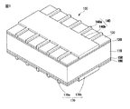
- 第1導電型の基板と、
前記基板の第1面に位置し、第1導電型とは異なる第2導電型の不純物を含有する第1ドーピング部と、
前記第1ドーピング部と電気的に接続された第1電極部と
を含み、
前記第1電極部は、熱硬化性樹脂と、前記熱硬化性樹脂内に分散された第1導電性粒子と、第2導電性粒子と、前記第2導電性粒子と前記第1ドーピング部の接触界面に位置するシリサイドを含み、
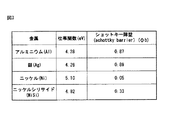
前記第1導電性粒子は銀(Ag)から構成され、前記第2導電性粒子は前記第1導電性粒子と比べて高い仕事関数を有するニッケル(Ni)から構成され、
前記ニッケルは、銀とニッケルを合せた全重量に対して15重量%〜25重量%の割合で含有される、太陽電池。 - 前記第1ドーピング部と接触する界面に形成されたシリサイドがニッケルシリサイドから構成される、請求項1記載の太陽電池。
- 前記ニッケルシリサイド(NS)は前記ニッケル(Ni)に比べて仕事関数が低くショットキー障壁が高いが、前記ニッケル(Ni)に比べて低い比抵抗を有する、請求項2記載の太陽電池。
- 前記ニッケルは、
2μm〜10μmの大きさを有する、請求項1記載の太陽電池。 - 前記熱硬化性樹脂は、
モノマー系のエポキシ樹脂またはアクリル樹脂を含む、請求項1記載の太陽電池。 - 前記第1ドーピング部は、
エミッタ部から形成される、請求項1記載の太陽電池。 - 前記エミッタ部には誘電層が形成される、請求項6記載の太陽電池。
- 前記第1電極部は、第1方向に延長された複数の第1フィンガー電極と、前記第1フィンガー電極と交差する第2方向に延長された複数の第1バスバー電極を含む、請求項7記載の太陽電池。
- 前記基板の第1面の反対側に位置する第2面に位置し、前記第1導電型の不純物を前記基板に比べて高濃度で含有する第2ドーピング部と、
前記第2ドーピング部と電気的に接続された第2電極部と
をさらに含み、
前記第2電極部は、前記第1導電性粒子、前記第2導電性粒子、前記シリサイド及び前記熱硬化性樹脂を含む、請求項1記載の太陽電池。 - 前記第2ドーピング部は後面電界部で形成される、請求項9記載の太陽電池。
- 前記後面電界部には、誘電層が形成される、請求項10記載の太陽電池。
- 前記第2電極部は、第1方向に延長された複数の第2フィンガー電極と前記第2フィンガー電極と交差する第2方向に延長された複数の第2バスバー電極を含む、請求項11記載の太陽電池。
- 第1導電型を有する基板の第1面に前記第1導電型とは異なる第2導電型の不純物を含有する第1ドーピング部を形成する段階と、
前記第1ドーピング部の一部を露出する開口部を備える誘電層を前記第1ドーピング部上に形成する段階と、
前記第1ドーピング部と電気的に接続された第1電極部を形成する段階と、を含み、
前記第1電極部を形成する段階は、
熱硬化性樹脂、前記熱硬化性樹脂内に分散された第1導電性粒子と、前記熱硬化性樹脂内に分散され、前記第1導電性粒子に比べて高い仕事関数を有する第2導電性粒子を含む電極ペーストを前記開口部を介して露出された前記第1ドーピング部に印刷する段階と、
前記電極ペーストを熱処理して硬化する段階と、
前記第2導電性粒子と、前記第1ドーピング部が接触する界面にシリサイドを形成する段階と
を含み、
前記第1電極部は、熱硬化性樹脂と、前記熱硬化性樹脂内に分散された第1導電性粒子と、第2導電性粒子と、前記第2導電性粒子と第1ドーピング部の接触界面に位置するシリサイドを含み、
前記第1導電性粒子は銀(Ag)から構成され、前記第2導電性粒子は前記第1導電性粒子と比べて高い仕事関数を有するニッケル(Ni)から構成され、
前記ニッケルは、銀とニッケルを合せた全重量に対して15重量%〜25重量%の割合で含有される、太陽電池の製造方法。 - 前記シリサイドを形成する段階は、前記ニッケルから構成された第2導電性粒子を利用して、前記第2導電性粒子が、前記第1ドーピング部と接触する界面にニッケルシリサイドを形成する段階を含む、請求項13記載の太陽電池の製造方法。
- 前記シリサイド(NS)は、前記ニッケル(Ni)に比べて仕事関数が低くショットキー障壁が高いが、前記ニッケル(Ni)に比べて低い比抵抗を有する、請求項14記載の太陽電池の製造方法。
- 230℃〜260℃の温度で前記電極ペーストを熱処理して硬化する、請求項15記載の太陽電池の製造方法。
- 前記ニッケルシリサイドを形成する段階は、前記基板を350℃〜400℃の温度に加熱することを含む、請求項16記載の太陽電池の製造方法。
- 前記第1ドーピング部をエミッタ部で形成する、請求項13記載の太陽電池の製造方法。
Applications Claiming Priority (2)
| Application Number | Priority Date | Filing Date | Title |
|---|---|---|---|
| KR1020130056314A KR101614186B1 (ko) | 2013-05-20 | 2013-05-20 | 태양전지 및 이의 제조 방법 |
| KR10-2013-0056314 | 2013-05-20 |
Publications (2)
| Publication Number | Publication Date |
|---|---|
| JP2014229904A JP2014229904A (ja) | 2014-12-08 |
| JP5952336B2 true JP5952336B2 (ja) | 2016-07-13 |
Family
ID=50390981
Family Applications (1)
| Application Number | Title | Priority Date | Filing Date |
|---|---|---|---|
| JP2014103448A Active JP5952336B2 (ja) | 2013-05-20 | 2014-05-19 | 太陽電池及びその製造方法 |
Country Status (5)
| Country | Link |
|---|---|
| US (1) | US11004988B2 (ja) |
| EP (1) | EP2806465B1 (ja) |
| JP (1) | JP5952336B2 (ja) |
| KR (1) | KR101614186B1 (ja) |
| CN (1) | CN104183656B (ja) |
Families Citing this family (4)
| Publication number | Priority date | Publication date | Assignee | Title |
|---|---|---|---|---|
| DE202015102238U1 (de) * | 2015-05-04 | 2015-06-01 | Solarworld Innovations Gmbh | Photovoltaik-Zelle und Photovoltaik-Modul |
| CN117041574A (zh) | 2016-10-28 | 2023-11-10 | 韩国电子通信研究院 | 视频编码/解码方法和设备以及存储比特流的记录介质 |
| KR101980946B1 (ko) * | 2016-11-11 | 2019-05-21 | 삼성에스디아이 주식회사 | 태양전지용 전면 전극 및 이를 포함하는 태양전지 |
| KR20210103850A (ko) * | 2020-02-14 | 2021-08-24 | 엘지전자 주식회사 | 태양 전지, 그리고 태양 전지 패널 및 이의 제조 방법 |
Family Cites Families (21)
| Publication number | Priority date | Publication date | Assignee | Title |
|---|---|---|---|---|
| JPS5896777A (ja) | 1981-12-03 | 1983-06-08 | Mitsubishi Electric Corp | 太陽電池 |
| JP3254044B2 (ja) | 1993-06-16 | 2002-02-04 | ナミックス株式会社 | 太陽電池用電極 |
| JP3557148B2 (ja) | 2000-02-21 | 2004-08-25 | 三洋電機株式会社 | 太陽電池モジュール |
| US8575474B2 (en) | 2006-03-20 | 2013-11-05 | Heracus Precious Metals North America Conshohocken LLC | Solar cell contacts containing aluminum and at least one of boron, titanium, nickel, tin, silver, gallium, zinc, indium and copper |
| JP2008135654A (ja) | 2006-11-29 | 2008-06-12 | Sanyo Electric Co Ltd | 太陽電池モジュール |
| TWI330998B (en) * | 2007-01-16 | 2010-09-21 | Chimei Innolux Corp | Top emitter organic electroluminescent display |
| JP4992449B2 (ja) * | 2007-02-06 | 2012-08-08 | 株式会社村田製作所 | 厚膜導体組成物および太陽電池セルの裏面Ag電極 |
| US20100037941A1 (en) * | 2008-08-13 | 2010-02-18 | E. I. Du Pont De Nemours And Company | Compositions and processes for forming photovoltaic devices |
| CN101752452A (zh) * | 2008-12-01 | 2010-06-23 | 台湾茂矽电子股份有限公司 | 双面太阳能电池的制造方法 |
| US8710355B2 (en) | 2008-12-22 | 2014-04-29 | E I Du Pont De Nemours And Company | Compositions and processes for forming photovoltaic devices |
| JP2010182935A (ja) * | 2009-02-06 | 2010-08-19 | Sharp Corp | 薄膜太陽電池の製造方法 |
| JP5144857B2 (ja) | 2010-03-01 | 2013-02-13 | 株式会社ノリタケカンパニーリミテド | 太陽電池用導電性ペースト組成物 |
| TWI495121B (zh) | 2010-07-09 | 2015-08-01 | Sakamoto Jun | A panel, a panel manufacturing method, a solar cell module, a printing apparatus, and a printing method |
| US20120037216A1 (en) | 2010-08-13 | 2012-02-16 | Samsung Electronics Co., Ltd. | Conductive paste and electronic device and solar cell including an electrode formed using the conductive paste |
| KR101665722B1 (ko) | 2010-09-27 | 2016-10-24 | 엘지전자 주식회사 | 태양 전지 및 이의 제조 방법 |
| US20120142140A1 (en) * | 2010-12-02 | 2012-06-07 | Applied Nanotech Holdings, Inc. | Nanoparticle inks for solar cells |
| KR20120079591A (ko) | 2011-01-05 | 2012-07-13 | 엘지전자 주식회사 | 태양전지 및 그 제조 방법 |
| KR20120091629A (ko) * | 2011-02-09 | 2012-08-20 | 엘지전자 주식회사 | 태양전지 |
| DE102011016335B4 (de) | 2011-04-07 | 2013-10-02 | Universität Konstanz | Nickelhaltige und ätzende druckbare Paste sowie Verfahren zur Bildung von elektrischen Kontakten beim Herstellen einer Solarzelle |
| US8901414B2 (en) * | 2011-09-14 | 2014-12-02 | International Business Machines Corporation | Photovoltaic cells with copper grid |
| CN104011882A (zh) * | 2012-01-12 | 2014-08-27 | 应用材料公司 | 制造太阳能电池装置的方法 |
-
2013
- 2013-05-20 KR KR1020130056314A patent/KR101614186B1/ko active IP Right Grant
-
2014
- 2014-03-20 US US14/221,111 patent/US11004988B2/en active Active
- 2014-03-28 EP EP14001166.9A patent/EP2806465B1/en active Active
- 2014-05-19 JP JP2014103448A patent/JP5952336B2/ja active Active
- 2014-05-20 CN CN201410214046.3A patent/CN104183656B/zh active Active
Also Published As
| Publication number | Publication date |
|---|---|
| EP2806465B1 (en) | 2017-01-04 |
| US20140338738A1 (en) | 2014-11-20 |
| EP2806465A2 (en) | 2014-11-26 |
| EP2806465A3 (en) | 2015-04-01 |
| KR101614186B1 (ko) | 2016-04-20 |
| CN104183656B (zh) | 2017-01-18 |
| JP2014229904A (ja) | 2014-12-08 |
| KR20140136562A (ko) | 2014-12-01 |
| CN104183656A (zh) | 2014-12-03 |
| US11004988B2 (en) | 2021-05-11 |
Similar Documents
| Publication | Publication Date | Title |
|---|---|---|
| JP5302414B2 (ja) | 太陽電池及びその製造方法 | |
| CN102983209B (zh) | 太阳能电池及其制造方法 | |
| US8039292B2 (en) | Holey electrode grids for photovoltaic cells with subwavelength and superwavelength feature sizes | |
| CN102428574A (zh) | 具有互连器的太阳能电池组件及其制造方法 | |
| JP5746263B2 (ja) | 太陽電池及びその製造方法 | |
| WO2017002927A1 (ja) | 太陽電池および太陽電池モジュール | |
| EP2458649B1 (en) | Solar cell | |
| US9337357B2 (en) | Bifacial solar cell module | |
| KR101738000B1 (ko) | 태양 전지 및 그 제조 방법 | |
| CN103515456B (zh) | 太阳能电池 | |
| US20120055538A1 (en) | Solar cell module | |
| JP5952336B2 (ja) | 太陽電池及びその製造方法 | |
| KR101666748B1 (ko) | 페로브스카이트 태양 전지 모듈 | |
| CN103943710B (zh) | 太阳能电池及其制造方法 | |
| JP6810708B2 (ja) | 誘起結合を有するバックコンタクト型光電池 | |
| JP2019204870A (ja) | 太陽電池素子および太陽電池素子の製造方法 | |
| KR100990108B1 (ko) | 태양 전지 및 그 제조 방법 | |
| KR101003808B1 (ko) | Pn접합 및 쇼트키 접합을 갖는 다중 태양 전지 및 이의 제조 방법 | |
| US20120192942A1 (en) | Solar cell and method for manufacturing the same | |
| US9209335B2 (en) | Solar cell system | |
| KR101852237B1 (ko) | 페로브스카이트 태양 전지 모듈 | |
| KR101186242B1 (ko) | 입체 패턴을 갖는 광전 소자 및 이의 제조 방법 | |
| KR20130085631A (ko) | 양면 수광형 태양전지 | |
| TWI733970B (zh) | 太陽能電池及其操作方法 | |
| TWM542861U (zh) | 太陽能電池 |
Legal Events
| Date | Code | Title | Description |
|---|---|---|---|
| A977 | Report on retrieval |
Free format text: JAPANESE INTERMEDIATE CODE: A971007 Effective date: 20150319 |
|
| A131 | Notification of reasons for refusal |
Free format text: JAPANESE INTERMEDIATE CODE: A131 Effective date: 20150324 |
|
| A521 | Request for written amendment filed |
Free format text: JAPANESE INTERMEDIATE CODE: A523 Effective date: 20150624 |
|
| A131 | Notification of reasons for refusal |
Free format text: JAPANESE INTERMEDIATE CODE: A131 Effective date: 20151110 |
|
| A521 | Request for written amendment filed |
Free format text: JAPANESE INTERMEDIATE CODE: A523 Effective date: 20160108 |
|
| TRDD | Decision of grant or rejection written | ||
| A01 | Written decision to grant a patent or to grant a registration (utility model) |
Free format text: JAPANESE INTERMEDIATE CODE: A01 Effective date: 20160510 |
|
| A61 | First payment of annual fees (during grant procedure) |
Free format text: JAPANESE INTERMEDIATE CODE: A61 Effective date: 20160609 |
|
| R150 | Certificate of patent or registration of utility model |
Ref document number: 5952336 Country of ref document: JP Free format text: JAPANESE INTERMEDIATE CODE: R150 |
|
| R250 | Receipt of annual fees |
Free format text: JAPANESE INTERMEDIATE CODE: R250 |
|
| R250 | Receipt of annual fees |
Free format text: JAPANESE INTERMEDIATE CODE: R250 |
|
| R250 | Receipt of annual fees |
Free format text: JAPANESE INTERMEDIATE CODE: R250 |
|
| R250 | Receipt of annual fees |
Free format text: JAPANESE INTERMEDIATE CODE: R250 |
|
| S111 | Request for change of ownership or part of ownership |
Free format text: JAPANESE INTERMEDIATE CODE: R313113 |
|
| R350 | Written notification of registration of transfer |
Free format text: JAPANESE INTERMEDIATE CODE: R350 |
|
| R250 | Receipt of annual fees |
Free format text: JAPANESE INTERMEDIATE CODE: R250 |
|
| S533 | Written request for registration of change of name |
Free format text: JAPANESE INTERMEDIATE CODE: R313533 |
|
| R350 | Written notification of registration of transfer |
Free format text: JAPANESE INTERMEDIATE CODE: R350 |
|
| S111 | Request for change of ownership or part of ownership |
Free format text: JAPANESE INTERMEDIATE CODE: R313113 |
|
| R350 | Written notification of registration of transfer |
Free format text: JAPANESE INTERMEDIATE CODE: R350 |
|
| R250 | Receipt of annual fees |
Free format text: JAPANESE INTERMEDIATE CODE: R250 |