WO2014148065A1 - Cellule solaire - Google Patents
Cellule solaire Download PDFInfo
- Publication number
- WO2014148065A1 WO2014148065A1 PCT/JP2014/050102 JP2014050102W WO2014148065A1 WO 2014148065 A1 WO2014148065 A1 WO 2014148065A1 JP 2014050102 W JP2014050102 W JP 2014050102W WO 2014148065 A1 WO2014148065 A1 WO 2014148065A1
- Authority
- WO
- WIPO (PCT)
- Prior art keywords
- solar cell
- layer
- receiving surface
- light
- sealing material
- Prior art date
Links
- 239000003566 sealing material Substances 0.000 claims abstract description 88
- 238000009792 diffusion process Methods 0.000 claims abstract description 66
- 239000010410 layer Substances 0.000 claims description 185
- 239000000758 substrate Substances 0.000 claims description 113
- 229920005989 resin Polymers 0.000 claims description 63
- 239000011347 resin Substances 0.000 claims description 63
- 239000012535 impurity Substances 0.000 claims description 28
- -1 titanium alkoxide Chemical class 0.000 claims description 17
- 238000010438 heat treatment Methods 0.000 claims description 13
- 229920005672 polyolefin resin Polymers 0.000 claims description 13
- 239000004065 semiconductor Substances 0.000 claims description 13
- 239000002356 single layer Substances 0.000 claims description 10
- 150000001875 compounds Chemical class 0.000 claims description 8
- 239000010936 titanium Substances 0.000 claims description 7
- 229910052719 titanium Inorganic materials 0.000 claims description 7
- LFQSCWFLJHTTHZ-UHFFFAOYSA-N Ethanol Chemical compound CCO LFQSCWFLJHTTHZ-UHFFFAOYSA-N 0.000 claims description 6
- 230000007774 longterm Effects 0.000 abstract description 23
- XUIMIQQOPSSXEZ-UHFFFAOYSA-N Silicon Chemical compound [Si] XUIMIQQOPSSXEZ-UHFFFAOYSA-N 0.000 description 81
- 229910052710 silicon Inorganic materials 0.000 description 81
- 239000010703 silicon Substances 0.000 description 81
- 238000002161 passivation Methods 0.000 description 66
- 238000012986 modification Methods 0.000 description 23
- 230000004048 modification Effects 0.000 description 23
- 239000000243 solution Substances 0.000 description 21
- 238000000034 method Methods 0.000 description 19
- 238000012360 testing method Methods 0.000 description 19
- 230000001681 protective effect Effects 0.000 description 18
- OAICVXFJPJFONN-UHFFFAOYSA-N Phosphorus Chemical compound [P] OAICVXFJPJFONN-UHFFFAOYSA-N 0.000 description 17
- 229910052698 phosphorus Inorganic materials 0.000 description 17
- 239000011574 phosphorus Substances 0.000 description 17
- 230000000052 comparative effect Effects 0.000 description 16
- 238000004519 manufacturing process Methods 0.000 description 16
- KFZMGEQAYNKOFK-UHFFFAOYSA-N Isopropanol Chemical group CC(C)O KFZMGEQAYNKOFK-UHFFFAOYSA-N 0.000 description 15
- VYPSYNLAJGMNEJ-UHFFFAOYSA-N Silicium dioxide Chemical compound O=[Si]=O VYPSYNLAJGMNEJ-UHFFFAOYSA-N 0.000 description 14
- 229910052814 silicon oxide Inorganic materials 0.000 description 14
- KRHYYFGTRYWZRS-UHFFFAOYSA-N Fluorane Chemical compound F KRHYYFGTRYWZRS-UHFFFAOYSA-N 0.000 description 13
- XLYOFNOQVPJJNP-UHFFFAOYSA-N water Chemical compound O XLYOFNOQVPJJNP-UHFFFAOYSA-N 0.000 description 13
- 239000004711 α-olefin Substances 0.000 description 13
- QVGXLLKOCUKJST-UHFFFAOYSA-N atomic oxygen Chemical compound [O] QVGXLLKOCUKJST-UHFFFAOYSA-N 0.000 description 12
- 229910052760 oxygen Inorganic materials 0.000 description 12
- 239000001301 oxygen Substances 0.000 description 12
- 239000000463 material Substances 0.000 description 11
- 238000007789 sealing Methods 0.000 description 11
- 238000005530 etching Methods 0.000 description 10
- 230000007423 decrease Effects 0.000 description 9
- 239000012298 atmosphere Substances 0.000 description 8
- 229920001577 copolymer Polymers 0.000 description 8
- VXUYXOFXAQZZMF-UHFFFAOYSA-N titanium(IV) isopropoxide Chemical compound CC(C)O[Ti](OC(C)C)(OC(C)C)OC(C)C VXUYXOFXAQZZMF-UHFFFAOYSA-N 0.000 description 8
- VXNZUUAINFGPBY-UHFFFAOYSA-N 1-Butene Chemical compound CCC=C VXNZUUAINFGPBY-UHFFFAOYSA-N 0.000 description 7
- 125000004432 carbon atom Chemical group C* 0.000 description 7
- 239000011521 glass Substances 0.000 description 7
- 230000003647 oxidation Effects 0.000 description 7
- 238000007254 oxidation reaction Methods 0.000 description 7
- VGGSQFUCUMXWEO-UHFFFAOYSA-N Ethene Chemical compound C=C VGGSQFUCUMXWEO-UHFFFAOYSA-N 0.000 description 6
- 239000005977 Ethylene Substances 0.000 description 6
- GWEVSGVZZGPLCZ-UHFFFAOYSA-N Titan oxide Chemical compound O=[Ti]=O GWEVSGVZZGPLCZ-UHFFFAOYSA-N 0.000 description 6
- 230000003667 anti-reflective effect Effects 0.000 description 6
- 230000000873 masking effect Effects 0.000 description 6
- 229910052751 metal Inorganic materials 0.000 description 6
- 239000002184 metal Substances 0.000 description 6
- QQONPFPTGQHPMA-UHFFFAOYSA-N propylene Natural products CC=C QQONPFPTGQHPMA-UHFFFAOYSA-N 0.000 description 6
- 125000004805 propylene group Chemical group [H]C([H])([H])C([H])([*:1])C([H])([H])[*:2] 0.000 description 6
- OGIDPMRJRNCKJF-UHFFFAOYSA-N titanium oxide Inorganic materials [Ti]=O OGIDPMRJRNCKJF-UHFFFAOYSA-N 0.000 description 6
- RYGMFSIKBFXOCR-UHFFFAOYSA-N Copper Chemical compound [Cu] RYGMFSIKBFXOCR-UHFFFAOYSA-N 0.000 description 5
- 229920000089 Cyclic olefin copolymer Polymers 0.000 description 5
- 239000004020 conductor Substances 0.000 description 5
- 238000011156 evaluation Methods 0.000 description 5
- 229910001392 phosphorus oxide Inorganic materials 0.000 description 5
- VSAISIQCTGDGPU-UHFFFAOYSA-N tetraphosphorus hexaoxide Chemical compound O1P(O2)OP3OP1OP2O3 VSAISIQCTGDGPU-UHFFFAOYSA-N 0.000 description 5
- CRSBERNSMYQZNG-UHFFFAOYSA-N 1-dodecene Chemical compound CCCCCCCCCCC=C CRSBERNSMYQZNG-UHFFFAOYSA-N 0.000 description 4
- GQEZCXVZFLOKMC-UHFFFAOYSA-N 1-hexadecene Chemical compound CCCCCCCCCCCCCCC=C GQEZCXVZFLOKMC-UHFFFAOYSA-N 0.000 description 4
- LIKMAJRDDDTEIG-UHFFFAOYSA-N 1-hexene Chemical compound CCCCC=C LIKMAJRDDDTEIG-UHFFFAOYSA-N 0.000 description 4
- KWKAKUADMBZCLK-UHFFFAOYSA-N 1-octene Chemical compound CCCCCCC=C KWKAKUADMBZCLK-UHFFFAOYSA-N 0.000 description 4
- HFDVRLIODXPAHB-UHFFFAOYSA-N 1-tetradecene Chemical compound CCCCCCCCCCCCC=C HFDVRLIODXPAHB-UHFFFAOYSA-N 0.000 description 4
- WSSSPWUEQFSQQG-UHFFFAOYSA-N 4-methyl-1-pentene Chemical compound CC(C)CC=C WSSSPWUEQFSQQG-UHFFFAOYSA-N 0.000 description 4
- BQCADISMDOOEFD-UHFFFAOYSA-N Silver Chemical compound [Ag] BQCADISMDOOEFD-UHFFFAOYSA-N 0.000 description 4
- 239000007864 aqueous solution Substances 0.000 description 4
- 238000005229 chemical vapour deposition Methods 0.000 description 4
- 239000011889 copper foil Substances 0.000 description 4
- YWEUIGNSBFLMFL-UHFFFAOYSA-N diphosphonate Chemical compound O=P(=O)OP(=O)=O YWEUIGNSBFLMFL-UHFFFAOYSA-N 0.000 description 4
- CCCMONHAUSKTEQ-UHFFFAOYSA-N octadec-1-ene Chemical compound CCCCCCCCCCCCCCCCC=C CCCMONHAUSKTEQ-UHFFFAOYSA-N 0.000 description 4
- YWAKXRMUMFPDSH-UHFFFAOYSA-N pentene Chemical compound CCCC=C YWAKXRMUMFPDSH-UHFFFAOYSA-N 0.000 description 4
- DLYUQMMRRRQYAE-UHFFFAOYSA-N phosphorus pentoxide Inorganic materials O1P(O2)(=O)OP3(=O)OP1(=O)OP2(=O)O3 DLYUQMMRRRQYAE-UHFFFAOYSA-N 0.000 description 4
- 229920000139 polyethylene terephthalate Polymers 0.000 description 4
- 239000005020 polyethylene terephthalate Substances 0.000 description 4
- 229910052709 silver Inorganic materials 0.000 description 4
- 239000004332 silver Substances 0.000 description 4
- ZOXJGFHDIHLPTG-UHFFFAOYSA-N Boron Chemical compound [B] ZOXJGFHDIHLPTG-UHFFFAOYSA-N 0.000 description 3
- PXHVJJICTQNCMI-UHFFFAOYSA-N Nickel Chemical compound [Ni] PXHVJJICTQNCMI-UHFFFAOYSA-N 0.000 description 3
- KDLHZDBZIXYQEI-UHFFFAOYSA-N Palladium Chemical compound [Pd] KDLHZDBZIXYQEI-UHFFFAOYSA-N 0.000 description 3
- 239000004734 Polyphenylene sulfide Substances 0.000 description 3
- 239000004743 Polypropylene Substances 0.000 description 3
- KWYUFKZDYYNOTN-UHFFFAOYSA-M Potassium hydroxide Chemical compound [OH-].[K+] KWYUFKZDYYNOTN-UHFFFAOYSA-M 0.000 description 3
- HEMHJVSKTPXQMS-UHFFFAOYSA-M Sodium hydroxide Chemical compound [OH-].[Na+] HEMHJVSKTPXQMS-UHFFFAOYSA-M 0.000 description 3
- 239000004809 Teflon Substances 0.000 description 3
- 229920006362 Teflon® Polymers 0.000 description 3
- 239000000654 additive Substances 0.000 description 3
- 229910052782 aluminium Inorganic materials 0.000 description 3
- XAGFODPZIPBFFR-UHFFFAOYSA-N aluminium Chemical compound [Al] XAGFODPZIPBFFR-UHFFFAOYSA-N 0.000 description 3
- 229910052796 boron Inorganic materials 0.000 description 3
- IAQRGUVFOMOMEM-UHFFFAOYSA-N butene Natural products CC=CC IAQRGUVFOMOMEM-UHFFFAOYSA-N 0.000 description 3
- 238000010586 diagram Methods 0.000 description 3
- 229920001519 homopolymer Polymers 0.000 description 3
- BHEPBYXIRTUNPN-UHFFFAOYSA-N hydridophosphorus(.) (triplet) Chemical compound [PH] BHEPBYXIRTUNPN-UHFFFAOYSA-N 0.000 description 3
- 239000000178 monomer Substances 0.000 description 3
- BASFCYQUMIYNBI-UHFFFAOYSA-N platinum Chemical compound [Pt] BASFCYQUMIYNBI-UHFFFAOYSA-N 0.000 description 3
- 229920001083 polybutene Polymers 0.000 description 3
- 229920000069 polyphenylene sulfide Polymers 0.000 description 3
- 229920001155 polypropylene Polymers 0.000 description 3
- 239000000523 sample Substances 0.000 description 3
- 238000007650 screen-printing Methods 0.000 description 3
- AFFLGGQVNFXPEV-UHFFFAOYSA-N 1-decene Chemical compound CCCCCCCCC=C AFFLGGQVNFXPEV-UHFFFAOYSA-N 0.000 description 2
- LDTAOIUHUHHCMU-UHFFFAOYSA-N 3-methylpent-1-ene Chemical compound CCC(C)C=C LDTAOIUHUHHCMU-UHFFFAOYSA-N 0.000 description 2
- 229910000838 Al alloy Inorganic materials 0.000 description 2
- 229920002799 BoPET Polymers 0.000 description 2
- NBIIXXVUZAFLBC-UHFFFAOYSA-N Phosphoric acid Chemical compound OP(O)(O)=O NBIIXXVUZAFLBC-UHFFFAOYSA-N 0.000 description 2
- 239000004698 Polyethylene Substances 0.000 description 2
- 239000004642 Polyimide Substances 0.000 description 2
- 230000000996 additive effect Effects 0.000 description 2
- 239000000853 adhesive Substances 0.000 description 2
- 230000001070 adhesive effect Effects 0.000 description 2
- 239000010949 copper Substances 0.000 description 2
- 239000003431 cross linking reagent Substances 0.000 description 2
- 238000011161 development Methods 0.000 description 2
- 238000009826 distribution Methods 0.000 description 2
- 229940069096 dodecene Drugs 0.000 description 2
- 238000001035 drying Methods 0.000 description 2
- 230000000694 effects Effects 0.000 description 2
- 239000008393 encapsulating agent Substances 0.000 description 2
- 239000011888 foil Substances 0.000 description 2
- 239000010931 gold Substances 0.000 description 2
- 238000009434 installation Methods 0.000 description 2
- TVMXDCGIABBOFY-UHFFFAOYSA-N n-Octanol Natural products CCCCCCCC TVMXDCGIABBOFY-UHFFFAOYSA-N 0.000 description 2
- 229920000573 polyethylene Polymers 0.000 description 2
- 229920013716 polyethylene resin Polymers 0.000 description 2
- 229920001721 polyimide Polymers 0.000 description 2
- 229920002620 polyvinyl fluoride Polymers 0.000 description 2
- 238000010248 power generation Methods 0.000 description 2
- 238000005215 recombination Methods 0.000 description 2
- 230000006798 recombination Effects 0.000 description 2
- 229910000679 solder Inorganic materials 0.000 description 2
- 230000003595 spectral effect Effects 0.000 description 2
- 238000004528 spin coating Methods 0.000 description 2
- 239000002562 thickening agent Substances 0.000 description 2
- DDFHBQSCUXNBSA-UHFFFAOYSA-N 5-(5-carboxythiophen-2-yl)thiophene-2-carboxylic acid Chemical compound S1C(C(=O)O)=CC=C1C1=CC=C(C(O)=O)S1 DDFHBQSCUXNBSA-UHFFFAOYSA-N 0.000 description 1
- 239000004925 Acrylic resin Substances 0.000 description 1
- 229920000178 Acrylic resin Polymers 0.000 description 1
- 229910052581 Si3N4 Inorganic materials 0.000 description 1
- 229910007116 SnPb Inorganic materials 0.000 description 1
- ATJFFYVFTNAWJD-UHFFFAOYSA-N Tin Chemical compound [Sn] ATJFFYVFTNAWJD-UHFFFAOYSA-N 0.000 description 1
- 238000010306 acid treatment Methods 0.000 description 1
- 229910000147 aluminium phosphate Inorganic materials 0.000 description 1
- LDDQLRUQCUTJBB-UHFFFAOYSA-O azanium;hydrofluoride Chemical compound [NH4+].F LDDQLRUQCUTJBB-UHFFFAOYSA-O 0.000 description 1
- 230000015572 biosynthetic process Effects 0.000 description 1
- 150000001639 boron compounds Chemical class 0.000 description 1
- DQXBYHZEEUGOBF-UHFFFAOYSA-N but-3-enoic acid;ethene Chemical compound C=C.OC(=O)CC=C DQXBYHZEEUGOBF-UHFFFAOYSA-N 0.000 description 1
- 229920005549 butyl rubber Polymers 0.000 description 1
- 239000000969 carrier Substances 0.000 description 1
- 230000015556 catabolic process Effects 0.000 description 1
- 239000011248 coating agent Substances 0.000 description 1
- 238000000576 coating method Methods 0.000 description 1
- 238000010276 construction Methods 0.000 description 1
- 229910052802 copper Inorganic materials 0.000 description 1
- 229910021419 crystalline silicon Inorganic materials 0.000 description 1
- 238000006731 degradation reaction Methods 0.000 description 1
- 229920001971 elastomer Polymers 0.000 description 1
- 239000012777 electrically insulating material Substances 0.000 description 1
- 230000007613 environmental effect Effects 0.000 description 1
- 239000003822 epoxy resin Substances 0.000 description 1
- 239000005038 ethylene vinyl acetate Substances 0.000 description 1
- 238000002474 experimental method Methods 0.000 description 1
- 238000010304 firing Methods 0.000 description 1
- 239000007789 gas Substances 0.000 description 1
- PCHJSUWPFVWCPO-UHFFFAOYSA-N gold Chemical compound [Au] PCHJSUWPFVWCPO-UHFFFAOYSA-N 0.000 description 1
- 229910052737 gold Inorganic materials 0.000 description 1
- 229910000040 hydrogen fluoride Inorganic materials 0.000 description 1
- 229910052738 indium Inorganic materials 0.000 description 1
- APFVFJFRJDLVQX-UHFFFAOYSA-N indium atom Chemical compound [In] APFVFJFRJDLVQX-UHFFFAOYSA-N 0.000 description 1
- 238000007641 inkjet printing Methods 0.000 description 1
- JEIPFZHSYJVQDO-UHFFFAOYSA-N iron(III) oxide Inorganic materials O=[Fe]O[Fe]=O JEIPFZHSYJVQDO-UHFFFAOYSA-N 0.000 description 1
- 238000010030 laminating Methods 0.000 description 1
- 229920000092 linear low density polyethylene Polymers 0.000 description 1
- 239000004707 linear low-density polyethylene Substances 0.000 description 1
- 229920005679 linear ultra low density polyethylene Polymers 0.000 description 1
- 229920001684 low density polyethylene Polymers 0.000 description 1
- 239000004702 low-density polyethylene Substances 0.000 description 1
- 238000002156 mixing Methods 0.000 description 1
- 239000000203 mixture Substances 0.000 description 1
- 238000000465 moulding Methods 0.000 description 1
- 229910052759 nickel Inorganic materials 0.000 description 1
- JRZJOMJEPLMPRA-UHFFFAOYSA-N olefin Natural products CCCCCCCC=C JRZJOMJEPLMPRA-UHFFFAOYSA-N 0.000 description 1
- 229920000620 organic polymer Polymers 0.000 description 1
- 239000003960 organic solvent Substances 0.000 description 1
- 229910052763 palladium Inorganic materials 0.000 description 1
- 238000000059 patterning Methods 0.000 description 1
- RLOWWWKZYUNIDI-UHFFFAOYSA-N phosphinic chloride Chemical compound ClP=O RLOWWWKZYUNIDI-UHFFFAOYSA-N 0.000 description 1
- 238000001259 photo etching Methods 0.000 description 1
- 229910052697 platinum Inorganic materials 0.000 description 1
- 229920001200 poly(ethylene-vinyl acetate) Polymers 0.000 description 1
- 229920005668 polycarbonate resin Polymers 0.000 description 1
- 239000004431 polycarbonate resin Substances 0.000 description 1
- 229920000647 polyepoxide Polymers 0.000 description 1
- 229920001225 polyester resin Polymers 0.000 description 1
- 239000004645 polyester resin Substances 0.000 description 1
- 229920005678 polyethylene based resin Polymers 0.000 description 1
- 239000011112 polyethylene naphthalate Substances 0.000 description 1
- 229920000642 polymer Polymers 0.000 description 1
- 229920005606 polypropylene copolymer Polymers 0.000 description 1
- 229920005990 polystyrene resin Polymers 0.000 description 1
- 239000002243 precursor Substances 0.000 description 1
- 238000003825 pressing Methods 0.000 description 1
- 230000002265 prevention Effects 0.000 description 1
- 238000012545 processing Methods 0.000 description 1
- 239000011342 resin composition Substances 0.000 description 1
- 239000005060 rubber Substances 0.000 description 1
- HQVNEWCFYHHQES-UHFFFAOYSA-N silicon nitride Chemical compound N12[Si]34N5[Si]62N3[Si]51N64 HQVNEWCFYHHQES-UHFFFAOYSA-N 0.000 description 1
- 229920002050 silicone resin Polymers 0.000 description 1
- 239000002904 solvent Substances 0.000 description 1
- 238000004544 sputter deposition Methods 0.000 description 1
- 239000000126 substance Substances 0.000 description 1
- 238000004381 surface treatment Methods 0.000 description 1
- 229920001897 terpolymer Polymers 0.000 description 1
- 229920002803 thermoplastic polyurethane Polymers 0.000 description 1
- XOLBLPGZBRYERU-UHFFFAOYSA-N tin dioxide Chemical compound O=[Sn]=O XOLBLPGZBRYERU-UHFFFAOYSA-N 0.000 description 1
- 229910001887 tin oxide Inorganic materials 0.000 description 1
- 238000004506 ultrasonic cleaning Methods 0.000 description 1
- 239000012808 vapor phase Substances 0.000 description 1
Images


Classifications
-
- H—ELECTRICITY
- H01—ELECTRIC ELEMENTS
- H01L—SEMICONDUCTOR DEVICES NOT COVERED BY CLASS H10
- H01L31/00—Semiconductor devices sensitive to infrared radiation, light, electromagnetic radiation of shorter wavelength or corpuscular radiation and specially adapted either for the conversion of the energy of such radiation into electrical energy or for the control of electrical energy by such radiation; Processes or apparatus specially adapted for the manufacture or treatment thereof or of parts thereof; Details thereof
- H01L31/02—Details
- H01L31/0224—Electrodes
- H01L31/022408—Electrodes for devices characterised by at least one potential jump barrier or surface barrier
- H01L31/022425—Electrodes for devices characterised by at least one potential jump barrier or surface barrier for solar cells
- H01L31/022441—Electrode arrangements specially adapted for back-contact solar cells
- H01L31/022458—Electrode arrangements specially adapted for back-contact solar cells for emitter wrap-through [EWT] type solar cells, e.g. interdigitated emitter-base back-contacts
-
- H—ELECTRICITY
- H01—ELECTRIC ELEMENTS
- H01L—SEMICONDUCTOR DEVICES NOT COVERED BY CLASS H10
- H01L31/00—Semiconductor devices sensitive to infrared radiation, light, electromagnetic radiation of shorter wavelength or corpuscular radiation and specially adapted either for the conversion of the energy of such radiation into electrical energy or for the control of electrical energy by such radiation; Processes or apparatus specially adapted for the manufacture or treatment thereof or of parts thereof; Details thereof
- H01L31/02—Details
- H01L31/0216—Coatings
- H01L31/02161—Coatings for devices characterised by at least one potential jump barrier or surface barrier
- H01L31/02167—Coatings for devices characterised by at least one potential jump barrier or surface barrier for solar cells
- H01L31/02168—Coatings for devices characterised by at least one potential jump barrier or surface barrier for solar cells the coatings being antireflective or having enhancing optical properties for the solar cells
-
- H—ELECTRICITY
- H01—ELECTRIC ELEMENTS
- H01L—SEMICONDUCTOR DEVICES NOT COVERED BY CLASS H10
- H01L31/00—Semiconductor devices sensitive to infrared radiation, light, electromagnetic radiation of shorter wavelength or corpuscular radiation and specially adapted either for the conversion of the energy of such radiation into electrical energy or for the control of electrical energy by such radiation; Processes or apparatus specially adapted for the manufacture or treatment thereof or of parts thereof; Details thereof
- H01L31/04—Semiconductor devices sensitive to infrared radiation, light, electromagnetic radiation of shorter wavelength or corpuscular radiation and specially adapted either for the conversion of the energy of such radiation into electrical energy or for the control of electrical energy by such radiation; Processes or apparatus specially adapted for the manufacture or treatment thereof or of parts thereof; Details thereof adapted as photovoltaic [PV] conversion devices
- H01L31/042—PV modules or arrays of single PV cells
- H01L31/048—Encapsulation of modules
- H01L31/0481—Encapsulation of modules characterised by the composition of the encapsulation material
-
- H—ELECTRICITY
- H01—ELECTRIC ELEMENTS
- H01L—SEMICONDUCTOR DEVICES NOT COVERED BY CLASS H10
- H01L31/00—Semiconductor devices sensitive to infrared radiation, light, electromagnetic radiation of shorter wavelength or corpuscular radiation and specially adapted either for the conversion of the energy of such radiation into electrical energy or for the control of electrical energy by such radiation; Processes or apparatus specially adapted for the manufacture or treatment thereof or of parts thereof; Details thereof
- H01L31/04—Semiconductor devices sensitive to infrared radiation, light, electromagnetic radiation of shorter wavelength or corpuscular radiation and specially adapted either for the conversion of the energy of such radiation into electrical energy or for the control of electrical energy by such radiation; Processes or apparatus specially adapted for the manufacture or treatment thereof or of parts thereof; Details thereof adapted as photovoltaic [PV] conversion devices
- H01L31/042—PV modules or arrays of single PV cells
- H01L31/05—Electrical interconnection means between PV cells inside the PV module, e.g. series connection of PV cells
- H01L31/0504—Electrical interconnection means between PV cells inside the PV module, e.g. series connection of PV cells specially adapted for series or parallel connection of solar cells in a module
- H01L31/0516—Electrical interconnection means between PV cells inside the PV module, e.g. series connection of PV cells specially adapted for series or parallel connection of solar cells in a module specially adapted for interconnection of back-contact solar cells
-
- Y—GENERAL TAGGING OF NEW TECHNOLOGICAL DEVELOPMENTS; GENERAL TAGGING OF CROSS-SECTIONAL TECHNOLOGIES SPANNING OVER SEVERAL SECTIONS OF THE IPC; TECHNICAL SUBJECTS COVERED BY FORMER USPC CROSS-REFERENCE ART COLLECTIONS [XRACs] AND DIGESTS
- Y02—TECHNOLOGIES OR APPLICATIONS FOR MITIGATION OR ADAPTATION AGAINST CLIMATE CHANGE
- Y02E—REDUCTION OF GREENHOUSE GAS [GHG] EMISSIONS, RELATED TO ENERGY GENERATION, TRANSMISSION OR DISTRIBUTION
- Y02E10/00—Energy generation through renewable energy sources
- Y02E10/50—Photovoltaic [PV] energy
Definitions
- the present invention relates to a solar cell.
- the above solar cell module is used outdoors for a long period of time, long-term reliability is required in all outdoor environments such as high temperature and high humidity.
- the solar cells constituting the solar cell module are mainly manufactured using crystalline silicon, it is considered that a relatively long life can be expected.
- the long-term reliability of the solar cell module is Improvements have been made with a focus on members other than solar cells constituting the battery module.
- PID Peak Induced Degradation
- Non-Patent Document 1 describes the cause of PID as follows.
- the frame side is grounded in parallel.
- a large potential difference is generated between the outer frame of the solar cell module and the inner solar cell.
- moisture adheres to the surface of the glass substrate that protects the light receiving surface of the solar cell module a leak current is generated between the frame and the solar cell via the moisture, and the leak current causes Electric charges accumulate on the light receiving surface of the solar battery cell.
- Patent Document 1 a solar cell array 100 in which a plurality of solar cells 101 are connected by an interconnector 254 is referred to as a light-receiving surface side transparent protective member 251.
- proposed solar cell module of the volume resistivity at 45 ° C. ⁇ 85 ° C. was sealed with 1 ⁇ 10 16 ⁇ ⁇ cm or more of the high-resistance sealing material 252 structure Has been.
- Patent Document 1 it is said that a decrease in output can be suppressed by preventing a leak current from the light receiving surface side of the solar cell array 100 with a high-resistance sealing material 252.
- the high-resistance sealing material 252 having a volume resistivity of 1 ⁇ 10 16 ⁇ ⁇ cm or more at 45 ° C. to 85 ° C. used in the solar cell module described in Patent Document 1 is very special. And since it was expensive, the manufacturing cost of the solar cell module could not be kept low.
- an object of the present invention is to provide a solar cell that can ensure long-term reliability without using a special and expensive sealing material.
- the present invention comprises a back electrode type solar cell and a sealing material provided on the light receiving surface of the back electrode type solar cell, the back electrode type solar cell comprising a first conductivity type semiconductor substrate, A first conductive type light receiving surface diffusion layer provided on the light receiving surface side surface of the semiconductor substrate, and a first conductive type impurity diffusion layer and a second conductive type provided on the surface opposite to the light receiving surface side of the semiconductor substrate.
- the sheet resistance of the light-receiving surface diffusion layer is 40 ⁇ / ⁇ or more and 80 ⁇ / ⁇ or less, and the volume resistivity at 85 ° C. of the sealing material is 1 ⁇ 10 16 ⁇ ⁇ cm or less. It is a solar cell. With such a configuration, long-term reliability of the solar cell can be ensured without using a special and expensive sealing material.
- FIG. 3 is a schematic plan view of the back surface of an example of a back electrode type solar battery cell used in the solar battery of Embodiment 1.
- FIG. (A) is a schematic cross-sectional view taken along II-II in FIG. 1, and (b) is a schematic enlarged cross-sectional view of a part of the light-receiving surface of the n-type silicon substrate shown in (a).
- (A)-(i) is typical sectional drawing illustrating about an example of the manufacturing method of the back electrode type photovoltaic cell used for the solar cell of Embodiment 1.
- FIG. 4 is a schematic plan view of the surface of an example of a wiring sheet used in the solar cell of Embodiment 1.
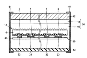
- FIG. 3 is a schematic cross-sectional view of the solar cell in the first embodiment.
- 6 is a schematic cross-sectional view of a modification of the solar cell of Embodiment 1.
- FIG. 6 is a schematic cross-sectional view of another modification of the solar cell in the first embodiment.
- FIG. 1 is typical sectional drawing of an example of the back electrode type photovoltaic cell used for the solar cell of Embodiment 2
- (b) is a part of light-receiving surface of the n-type silicon substrate shown to (a). It is a typical expanded sectional view of.
- (A)-(k) is typical sectional drawing illustrating about an example of the manufacturing method of the back surface electrode type photovoltaic cell used for the solar cell of Embodiment 2.
- FIG. In Embodiment 2 it is typical sectional drawing illustrating the process of sealing the back surface electrode type photovoltaic cell installed on the wiring sheet.
- 6 is a schematic cross-sectional view of a solar cell according to Embodiment 2.
- FIG. 6 is a schematic cross-sectional view of a modification of the solar cell of Embodiment 2.
- FIG. 6 is a schematic cross-sectional view of another modification of the solar cell of Embodiment 2.
- FIG. It is a typical block diagram illustrating a pseudo negative electrode ground test apparatus.
- FIG. 6 is a graph showing the relationship between the sheet resistance of the light-receiving surface diffusion layer of the back electrode type solar cells of Examples 1 to 8 and Comparative Examples 1 to 6 and the volume resistivity at 85 ° C. of the sealing material. It is a typical block diagram illustrating the process of sealing the solar cell array of the conventional solar cell module of patent document 1 with a sealing material.
- FIG. 1 the typical top view of the back surface of an example of the back electrode type solar cell used for the solar cell of Embodiment 1 is shown.
- the back electrode type solar cell 1 has a first conductivity type on the back surface which is the surface opposite to the light receiving surface side of the back electrode type solar cell 1 of the n-type silicon substrate 4 as the first conductivity type semiconductor substrate.
- the n-electrode 2 and the p-electrode 3 are alternately arranged on the back surface of the n-type silicon substrate 4. It is arranged.
- FIG. 2A shows a schematic cross-sectional view along II-II in FIG. 1, and FIG. 2B schematically shows a part of the light-receiving surface of the n-type silicon substrate 4 shown in FIG. 2A. An enlarged sectional view is shown. As shown in FIG. 2A, an uneven shape 5 is formed on the light receiving surface of the n-type silicon substrate 4.
- an n + layer 6 is formed as a light receiving surface diffusion layer which is an FSF layer.
- the n + layer 6 is a layer having the same n type conductivity type as the n type silicon substrate 4, and the n type impurity concentration of the n + layer 6 is higher than the n type impurity concentration of the n type silicon substrate 4. ing.
- a light-receiving surface passivation film 8 is formed on the n + layer 6.
- the light-receiving surface passivation film 8 is made of a silicon oxide film.
- the thickness of the light-receiving surface passivation film 8 is preferably 30 nm or more and 200 nm or less. When the thickness of the light-receiving surface passivation film 8 is 30 nm or more and 200 nm or less, the characteristics of the back electrode type solar cell 1 tend to be improved.
- an antireflection film 12 is formed on the light receiving surface passivation film 8.
- Antireflection film 12 includes an n-type impurity having the same n-type conductivity as n-type silicon substrate 4, and is made of, for example, a titanium oxide film containing phosphorus as an n-type impurity.
- the thickness of the antireflection film 12 can be, for example, 30 nm or more and 500 nm or less.
- phosphorus in the antireflection film 12 is contained as a phosphorus oxide in an amount of 15% by mass or more and 35% by mass or less of the antireflection film 7.
- 15 mass% or more and 35 mass% or less of the anti-reflective film 12 is contained as a phosphorus oxide that the content of the phosphorus oxide in the anti-reflective film 12 is 15 mass% or more and 35 mass% of the whole anti-reflective film 12. It means the following.
- an n ++ layer 10 which is an n-type impurity diffusion layer as a first conductivity-type impurity diffusion layer, and a second conductivity-type impurity diffusion layer are formed.
- P + layers 11 which are p-type impurity diffusion layers are alternately formed.
- a back surface passivation film 15 is formed on the back surface of the n type silicon substrate 4 by laminating a second back surface passivation film 14 and a first back surface passivation film 13 in this order from the n type silicon substrate 4 side.
- An n electrode 2 and a p electrode 3 are formed on the n ++ layer 10 and the p + layer 11 exposed from the back surface passivation film 15, respectively.
- the uneven shape 5 is formed on the light-receiving surface of the n-type silicon substrate 4 as shown in FIG. Form.
- a diffusion mask 22 is formed on the light receiving surface of the n-type silicon substrate 4, and a part of the back surface is formed.
- a diffusion mask 23 is formed, and then an n ++ layer 10 is formed on a part of the back surface of the n-type silicon substrate 4.
- the diffusion mask 24 is applied to the light-receiving surface of the n-type silicon substrate 4.
- a diffusion mask 25 is formed on a part of the back surface, and then a p + layer 11 is formed on a part of the back surface of the n-type silicon substrate 4.
- a solution 27 is applied to the light receiving surface of the n-type silicon substrate 4 and then dried.
- application and drying of the solution 27 can be performed, for example, as follows.
- a first back surface passivation film 13 that also serves as a diffusion mask such as a silicon oxide film having a thickness of 50 nm to 100 nm is formed on the back surface of the n-type silicon substrate 4.
- the first back surface passivation film 13 can be formed by, for example, CVD or SOG (spin-on-glass) coating and baking.
- a solution 27 containing a phosphorus-containing compound, titanium alkoxide, and alcohol is applied to the light-receiving surface of the n-type silicon substrate 4 by spin coating or the like and then dried.
- the compound containing phosphorus contained in the solution 27 for example, phosphorus pentoxide can be used.
- the titanium alkoxide for example, tetraisopropyl titanate can be used.
- alcohol isopropyl alcohol etc. can be used, for example.
- an n + layer 6, a light-receiving surface passivation film 8 and an antireflection film 12 are formed on the light-receiving surface of the n-type silicon substrate 4, and n
- a second back surface passivation film 14 is formed between the back surface of the mold silicon substrate 4 and the first back surface passivation film 13.
- the n + layer 6 and the antireflection film 12 can be formed by heat-treating the n-type silicon substrate 4 on which the solution 27 is applied to the light receiving surface, for example, at a temperature of 850 ° C. or more and 1000 ° C. or less. That is, by this heating, phosphorus diffuses from the solution 27 on the light receiving surface of the n-type silicon substrate 4 to form the n + layer 6 and the antireflection film 12 made of a titanium oxide film containing phosphorus.
- the light-receiving surface passivation film 8 and the second back surface passivation film 14 can be formed by performing thermal oxidation with oxygen or water vapor on the n-type silicon substrate 4 after the formation of the n + layer 6 and the antireflection film 12. it can. As a result, as shown in FIG. 3I, a light-receiving surface passivation film 8 is formed between the n + layer 6 on the light-receiving surface of the n-type silicon substrate 4 and the antireflection film 12, and an n-type silicon substrate is formed. 4, a second back surface passivation film 14 is formed between the back surface 4 and the first back surface passivation film 13.
- a laminated body of the first back surface passivation film 13 and the second back surface passivation film 14 is referred to as a back surface passivation film 15.
- the reason why the light-receiving surface passivation film 8 is formed between the n + layer 6 and the antireflection film 12 is that the film thickness of the antireflection film 12 in the concave portion of the concavo-convex shape 5 on the light receiving surface is increased and the antireflection film 12 is formed. It is considered that a silicon oxide film, which is the light-receiving surface passivation film 8, grows due to oxygen or water vapor entering from the portion where the crack is generated.
- the antireflection film 12 is thin at the convex portion of the concave-convex shape 5 on the light receiving surface, it is considered that oxygen or water vapor is transmitted and a silicon oxide film that is the light receiving surface passivation film 8 grows. Furthermore, the reason why the second back surface passivation film 14 is formed between the back surface of the n-type silicon substrate 4 and the first back surface passivation film 13 is that the first back surface passivation film on the back surface of the n-type silicon substrate 4 is used. Since 13 is a film formed by a CVD method or the like, it is considered that oxygen or water vapor passes through the inside of the first back surface passivation film 13, thereby growing a silicon oxide film as the second back surface passivation film 14. .
- the thickness of the light-receiving surface passivation film 8 is not less than 100 nm and not more than 200 nm, for example, and the thickness of the second back surface passivation film 14 is not less than 30 nm and not more than 100 nm on the n ++ layer 10, for example. On the layer 11, the thickness is 10 nm or more and 40 nm or less.
- the thermal oxidation of the n-type silicon substrate 4 with oxygen or water vapor for forming the light-receiving surface passivation film 8 and the second back surface passivation film 14 is performed by placing the n-type silicon substrate 4 in an oxygen atmosphere or a water vapor atmosphere. It can carry out by heat-processing in a state.
- the sheet resistance of the n + layer 6 is 40 ⁇ / ⁇ or more and 80 ⁇ / ⁇ or less. Note that the sheet resistance of the n + layer 6 can be appropriately adjusted by changing at least one of the phosphorus content in the solution 27, the temperature during the thermal oxidation, and the time, for example.
- the light-receiving surface passivation film 8 and the second back surface passivation film 14 are n-type silicon substrates by switching the atmosphere gas to an oxygen atmosphere or a water vapor atmosphere following the heat treatment for forming the n + layer 6 and the antireflection film 12. 4 can also be formed by performing thermal oxidation.
- a part of the back surface passivation film 15 is removed to expose a part of the n ++ layer 10 and a part of the p + layer 11 from the back surface passivation film 9. .
- the n electrode 2 is formed on the n + + layer 10 and the p electrode 3 is formed on the p + layer 11.
- the back electrode type solar cell 1 can be manufactured.
- the wiring sheet 30 includes an insulating substrate 31 and wirings 36 installed on the surface of the insulating substrate 31.
- the wiring 36 includes an n wiring 32, an n wiring 32 a, a p wiring 33, a p wiring 33 a, and a connection wiring 34.
- the n wiring 32, the n wiring 32a, the p wiring 33, the p wiring 33a, and the connection wiring 34 are conductive.
- the n wiring 32 and the p wiring 33 have a comb shape including a shape in which a plurality of rectangles are arranged in a direction orthogonal to the longitudinal direction of the rectangle.
- the n wiring 32a, the p wiring 33a, and the connection wiring 34 are strip-shaped.
- the adjacent n wiring 32 and the p wiring 33 other than the n wiring 32 a and the p wiring 33 a located at the end of the wiring sheet 30 are electrically connected by the connection wiring 34.
- the portions corresponding to the comb teeth (rectangular) of the comb-shaped n wiring 32 and the portions corresponding to the comb teeth (rectangular) of the comb-shaped p wiring 33 are alternately meshed one by one.
- the n wiring 32 and the p wiring 33 are arranged.
- a portion corresponding to the comb teeth of the comb-shaped n wiring 32 and a portion corresponding to the comb teeth of the comb-shaped p wiring 33 are alternately arranged at predetermined intervals. .
- at least one of the portions corresponding to the comb teeth of the n wiring 32 and the p wiring 33 may be alternately arranged instead of one.
- the insulating base material 31 can be used without particular limitation as long as it is an electrically insulating material.
- PET polyethylene terephthalate
- PEN polyethylene naphthalate
- PET polyphenylene sulfide
- a material containing at least one resin selected from the group consisting of PPS (Polyphenylene sulfide), polyvinyl fluoride (PVF) and polyimide (Polyimide) can be used.
- the thickness of the insulating substrate 31 is not particularly limited, and can be, for example, 25 ⁇ m or more and 150 ⁇ m or less.
- the insulating base 31 may have a single-layer structure consisting of only one layer or a multi-layer structure consisting of two or more layers.
- the material of the wiring 36 can be used without particular limitation as long as it is a conductive material.
- a conductive material For example, at least one selected from the group consisting of copper (Cu), aluminum (Al), and silver (Ag) is used.
- a metal containing, for example, can be used.
- the thickness of the wiring 36 is not particularly limited, and can be, for example, 10 ⁇ m or more and 50 ⁇ m or less.
- the shape of the wiring 36 is not limited to the shape described above, and can be set as appropriate.
- At least a part of the surface of the wiring 36 has, for example, nickel (Ni), gold (Au), platinum (Pt), palladium (Pd), silver (Ag), tin (Sn), SnPb solder, and ITO (Indium).
- a conductive substance containing at least one selected from the group consisting of Tin Oxide may be installed. In this case, there is a tendency that the electrical connection between the wiring 36 of the wiring sheet 30 and the electrode of the back electrode type solar battery cell to be described later can be improved, and the weather resistance of the wiring 36 can be improved.
- At least a part of the surface of the wiring 36 may be subjected to a surface treatment such as a rust prevention treatment or a blackening treatment.
- the wiring 36 may also have a single-layer structure consisting of only one layer, or a multi-layer structure consisting of two or more layers.
- an insulating substrate 31 such as a PET film is prepared, and a conductive material such as a metal foil or a metal plate is bonded to the entire surface of one surface of the insulating substrate 31.
- a conductive material such as a metal foil or a metal plate is bonded to the entire surface of one surface of the insulating substrate 31.
- a roll of an insulating base material cut to a predetermined width is pulled out, an adhesive is applied to one surface of the insulating base material 31, and a roll of metal foil cut slightly smaller than the width of the insulating base material 31 is applied.
- a wiring 36 including an n wiring 32, an n wiring 32a, a p wiring 33, a p wiring 33a, and a connection wiring 34 made of a conductive material is formed.
- the wiring sheet 30 having the configuration shown in FIG. 4 can be manufactured.
- FIG. 5 is a schematic plan view illustrating a state where the back electrode type solar cell 1 is installed on the wiring sheet 30 shown in FIG.
- the back electrode type solar cell 1 is installed on the wiring sheet 30 such that the back side of the back electrode type solar cell 1 faces the installation side of the wiring 36 of the wiring sheet 30.
- the back electrode type solar cell 1 is arranged on the wiring sheet 30 so that the n electrode 2 and the p electrode 3 of the back electrode type solar cell 1 are in contact with the n wiring 32 and the p wiring 33 of the wiring sheet 30, respectively.
- the n electrode 2 and the p electrode 3 may be mechanically and electrically connected to the n wiring 32 and the p wiring 33 by a conductive adhesive such as solder, for example.
- the n electrode 2 and the p electrode 3 are respectively connected to the n wiring 32 and the p electrode 3 by the shrinkage force when the insulating resin composition placed between the back electrode type solar cell 1 and the wiring sheet 30 is cured.
- the wiring 33 may be directly connected to be electrically connected and mechanically connected.
- the back electrode type solar cells installed so as to be adjacent to each other on the wiring sheet 30.
- the ones are electrically connected to each other.
- all the back surface electrode type photovoltaic cells 1 installed on the wiring sheet 30 are electrically connected in series.
- FIG. 6 is a schematic cross-sectional view illustrating the process of sealing the back electrode type solar battery cell 1 installed on the wiring sheet 30.
- the sheet-like first resin layer 40, the sheet-like second resin layer 41, and the transparent protective substrate. 42 are arranged in this order.
- the sheet-like first resin layer 40 and the back surface protection sheet 43 are arranged in this order from the wiring sheet 30 side.
- any substrate that is transparent to sunlight can be used without particular limitation, and for example, a glass substrate or the like can be used.
- the first resin layer 40 was selected from the group consisting of ethylene vinyl acetate resin, epoxy resin, acrylic resin, urethane resin, olefin resin, polyester resin, silicone resin, polystyrene resin, polycarbonate resin, and rubber resin, for example.
- a layer made of at least one transparent resin can be used.
- the second resin layer 41 a layer made of an olefin resin is preferably used.
- the olefin resin used for the second resin layer 41 for example, at least one selected from the group consisting of a polyethylene resin, a polypropylene resin, and a polybutene resin can be used.
- the polyethylene-based resin is an ethylene homopolymer or a copolymer of ethylene and one or more other monomers.
- the polypropylene resin is a homopolymer of propylene or a copolymer of propylene and one or more other monomers.
- the polybutene resin is a butene homopolymer or a copolymer of butene and one or more other monomers.
- polyethylene resin for example, polyethylene or ethylene- ⁇ -olefin copolymer can be used.
- polyethylene examples include low density polyethylene, linear low density polyethylene, and linear ultra-low density polyethylene.
- ethylene- ⁇ -olefin copolymer a copolymer comprising ethylene and at least one selected from ⁇ -olefins having 3 to 20 carbon atoms is preferably used, and ethylene and carbon atoms having 3 to 12 carbon atoms are used. It is more preferable to use a copolymer comprising at least one selected from ⁇ -olefins.
- the ⁇ -olefin include propylene, 1-butene, 1-pentene, 1-hexene, 1-octene, 4-methyl-1-pentene, 3-methyl-1-pentene, 1-decene and 1-dodecene. , 1-tetradecene, 1-hexadecene, 1-octadecene, and 1-eicosane can be used.
- polypropylene resin for example, a propylene- ⁇ -olefin copolymer or a terpolymer of propylene, ethylene, and ⁇ -olefin can be used.
- the propylene- ⁇ -olefin copolymer is a copolymer composed of at least one selected from propylene and ⁇ -olefin.
- a copolymer comprising at least one selected from ethylene and an ⁇ -olefin having 3 to 20 carbon atoms and propylene is preferably used, and ethylene and 4 to 4 carbon atoms are preferably used. It is more preferable to use a copolymer comprising at least one selected from 8 ⁇ -olefins and propylene.
- Examples of the ⁇ -olefin having 3 to 20 carbon atoms include propylene, 1-butene, 1-pentene, 1-hexene, 1-octene, 4-methyl-1-pentene, 3-methyl-1-pentene, 1 At least one selected from the group consisting of -decene, 1-dodecene, 1-tetradecene, 1-hexadecene, 1-octadecene and 1-eicosane can be used.
- polybutene resin for example, a crystalline copolymer comprising at least one selected from ethylene, propylene, and an olefin compound having 5 to 8 carbon atoms and butene can be used.
- the first resin layer 40 and the second resin layer 41 may contain conventionally known additives such as a crosslinking agent in addition to the above resin components. Further, the first resin layer 40 and the second resin layer 41 are formed into a sheet shape by, for example, mixing a conventionally known additive such as a crosslinking agent into the above resin component and molding the mixture into a predetermined shape. can do.
- a conventionally known additive such as a crosslinking agent
- any material can be used without particular limitation as long as it can protect the back surface of the first resin layer 40.
- a weathering film such as PET that has been conventionally used may be used. it can.
- the back surface protection sheet 43 includes a metal film such as aluminum, for example. Also good.
- the back surface protection sheet 43 such as the end face of the solar cell module with a moisture permeation preventing tape such as a butyl rubber tape.
- the back electrode type solar cell 1 sealed in the sealing material 50 is not limited to plural, and may be single.
- the sheet resistance of the n + layer 6 as the light-receiving surface diffusion layer of the back electrode type solar cell 1 is set to 40 ⁇ / ⁇ or more and 80 ⁇ / ⁇ or less, and the back electrode type solar cell 1
- the volume resistivity at 85 ° C. of the sealing material (second resin layer 41) provided on the light receiving surface is set to 1 ⁇ 10 16 ⁇ ⁇ cm or less.
- the sheet resistance of the n + layer 6 as the light-receiving surface diffusion layer is set to 40 ⁇ / ⁇ or more and 80 ⁇ / ⁇ or less, so that the light-receiving surface of the back electrode type solar cell 1 is obtained.
- the sheet resistance of the n + layer 6 as the light-receiving surface diffusion layer of the back electrode type solar cell 1 is less than 40 ⁇ / ⁇ , recombination in the n + layer 6 increases, so that the back electrode type The output of the solar battery cell 1 itself decreases.
- the sheet resistance of the n + layer 6 is higher than 80 ⁇ / ⁇ , a large potential difference is generated between the back electrode type solar cell 1 and the frame 61, and moisture or the like is present on the surface of the transparent protective substrate 42. If accumulated, charge accumulates in the light-receiving surface passivation film 8 of the back electrode type solar cell 1, and the function of the n + layer 6 as an FSF (Front Surface Field) deteriorates.
- FSF Front Surface Field
- the volume resistivity at 45 ° C. to 85 ° C. is as high as 1 ⁇ 10 16 ⁇ ⁇ cm or higher. Since it is possible to suppress a decrease in output due to PID or the like without using a special sealing material, the choice of sealing material provided on the light-receiving surface of the back electrode type solar cell 1 is more than conventional. It can be expanded and long-term reliability can be ensured.
- a high-resistance special resistance having a volume resistivity of 1 ⁇ 10 16 ⁇ ⁇ cm or more at 45 ° C. to 85 ° C.
- the manufacturing cost of the solar cell module can be kept low.
- the volume resistivity at 45 ° C. to 85 ° C. is as high as 1 ⁇ 10 16 ⁇ ⁇ cm or more, Since it is not necessary to use a sealing material that is very difficult to handle, the manufacturing efficiency of the solar cell module can be improved.
- the volume resistivity at 85 ° C. of the sealing material (second resin layer 41) provided on the light receiving surface of the back electrode type solar cell 1 is 1 ⁇ 10 12 ⁇ ⁇ cm or more and 1 ⁇ 10 16 ⁇ ⁇ cm or less, 1 ⁇ 10 15 ⁇ ⁇ 1 ⁇ more preferably not more than 10 16 Omega ⁇ cm or more cm, 2.8 ⁇ 10 15 ⁇ ⁇ cm or more 5.1 ⁇ 10 15 ⁇ ⁇ cm More preferably, it is as follows. In these cases, the long-term reliability of the solar cell of Embodiment 1 can be further improved without using a special and expensive sealing material.
- FIG. 8 shows a schematic cross-sectional view of a modification of the solar cell of the first embodiment.
- the sealing material 50 that seals the back electrode type solar cell 1 is the second resin on the light receiving surface of the back electrode type solar cell 1. It consists of the laminated body of the layer 41 and the 1st resin layer 40 on the wiring sheet 30, It is characterized by the above-mentioned.
- the sheet resistance of n + layer 6 as the light-receiving surface diffusion layer of back electrode type solar cell 1 is set to 40 ⁇ / ⁇ or more and 80 ⁇ / ⁇ or less. Therefore, a sealing material having a volume resistivity of 1 ⁇ 10 16 ⁇ ⁇ cm or less at 85 ° C. is used as the sealing material (second resin layer 41) provided on the light receiving surface of the back electrode type solar cell 1. be able to. Thereby, the modification of the solar cell of Embodiment 1 shown in FIG. 8 can also be set as the solar cell which can ensure long-term reliability, without using a special and expensive sealing material.
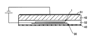
- FIG. 9 shows a schematic cross-sectional view of another modification of the solar cell of the first embodiment.
- the sealing material for sealing the back electrode type solar cell 1 is composed of a sealing material 52 made of a single layer of olefin resin. It is characterized by that.
- the sheet resistance of the n + layer 6 as the light-receiving surface diffusion layer of the back electrode type solar cell 1 is 40 ⁇ / ⁇ or more and 80 ⁇ / ⁇ or less. Therefore, as the sealing material provided on the light receiving surface of the back electrode type solar cell 1, the sealing material 52 made of a single layer of olefin resin having a volume resistivity at 85 ° C. of 1 ⁇ 10 16 ⁇ ⁇ cm or less. Can be used. Thereby, the other modification of the solar cell of Embodiment 1 shown in FIG. 9 can also be made into a solar cell which can ensure long-term reliability, without using a special and expensive sealing material.
- the first conductivity type is n-type and the second conductivity type is p-type.
- the present invention is not limited to this, and the first conductivity type is p-type.
- the second conductivity type may be n-type.
- the n-type silicon substrate is a p-type silicon substrate
- the light-receiving surface diffusion layer is a p + layer in which p-type impurities are diffused.
- the antireflection film is made of a titanium oxide film containing p-type impurities.
- the concept of the back electrode type solar cell which is one embodiment of the present invention includes a back electrode type solar cell having a configuration in which both an n electrode and a p electrode are formed only on one surface (back surface) of a semiconductor substrate.
- a solar cell having a configuration such as an MWT (Metal Wrap Through) type (a solar cell in which a part of an electrode is disposed in a through hole provided in a semiconductor substrate) is also included.
- MWT Metal Wrap Through
- FIG. 10 (a) shows a schematic cross-sectional view of an example of a back electrode type solar battery cell used in the solar battery of Embodiment 2
- FIG. 10 (b) shows an n-type silicon substrate shown in FIG. 10 (a).
- 4 is a schematic enlarged cross-sectional view of a part of the light receiving surface 4. As shown in FIG. 10A, an uneven shape 5 is formed on the light receiving surface of the n-type silicon substrate 4.
- an n + layer 6 is formed as a light receiving surface diffusion layer which is an FSF layer.
- the n + layer 6 is a layer having the same n type conductivity type as the n type silicon substrate 4, and the n type impurity concentration of the n + layer 6 is higher than the n type impurity concentration of the n type silicon substrate 4. ing.
- a light-receiving surface passivation film 8 is formed on the n + layer 6.
- the light-receiving surface passivation film 8 is made of a silicon oxide film.
- the thickness of the light-receiving surface passivation film 8 is preferably 30 nm or more and 200 nm or less. When the thickness of the light-receiving surface passivation film 8 is 30 nm or more and 200 nm or less, the characteristics of the back electrode type solar battery cell 16 tend to be improved.
- an antireflection film 7 is formed on the light receiving surface passivation film 8.
- the antireflection film 7 includes an n-type impurity having the same n-type conductivity as that of the n-type silicon substrate 4 and is made of, for example, a titanium oxide film containing phosphorus as an n-type impurity.
- the thickness of the antireflection film 7 can be set to, for example, 0 nm or more and 500 nm or less.
- the location where the thickness of the antireflection film 7 is 0 nm means that the portion of the antireflection film 7 is not formed.
- phosphorus in the antireflection film 7 is contained as a phosphorus oxide in an amount of 15% by mass to 35% by mass of the antireflection film 7.
- 15 mass% or more and 35 mass% or less of the anti-reflective film 7 are contained as phosphorous oxide, when the content of phosphorus oxide in the anti-reflective film 7 is 15 mass% or more and 35 mass% of the whole anti-reflective film 7. It means the following.
- an n ++ layer 10 which is an n-type impurity diffusion layer as a first conductivity-type impurity diffusion layer, and a second conductivity-type impurity diffusion layer are formed.
- P + layers 11 which are p-type impurity diffusion layers are alternately formed.
- a back surface passivation film 9 made of a silicon oxide film is formed on a part of the back surface of the n-type silicon substrate 4.
- An n electrode 2 and a p electrode 3 are formed on the n ++ layer 10 and the p + layer 11 exposed from the back surface passivation film 9, respectively.
- a texture mask 21 is formed on the back surface of the n-type silicon substrate 4.
- a texture mask 21 for example, a silicon nitride film or the like can be used.
- the texture mask 21 can be formed by, for example, a CVD (Chemical Vapor Deposition) method or a sputtering method.
- an uneven shape 5 is formed on the light receiving surface of the n-type silicon substrate 4.
- the uneven shape 5 can have a texture structure, for example.
- the uneven shape 5 is formed by etching the light-receiving surface of the n-type silicon substrate 4 with a solution in which isopropyl alcohol is added to an alkaline aqueous solution such as a sodium hydroxide aqueous solution or a potassium hydroxide aqueous solution and heated to 70 ° C. or higher and 80 ° C. or lower. Can be formed.
- an n ++ layer 10 is formed on a part of the back surface of the n-type silicon substrate 4.
- the n ++ layer 10 can be formed as follows, for example.
- the texture mask 21 on the back surface of the n-type silicon substrate 4 is removed.
- a diffusion mask 22 such as a silicon oxide film is formed on the light receiving surface of the n-type silicon substrate 4.
- a diffusion mask 23 is formed by applying a masking paste to a region other than the region where the n ++ layer 10 is formed on the back surface of the n-type silicon substrate 4 and then heat-treating the masking paste.
- the n ++ layer 10 is formed by diffusing phosphorus from the diffusion mask 23 to the portion where the back surface of the n-type silicon substrate 4 is exposed by vapor phase diffusion using POCl 3 .
- the thing containing a solvent, a thickener, and a silicon oxide precursor etc. can be used, for example.
- a method for applying the masking paste for example, an ink jet printing method or a screen printing method can be used.
- a p + layer 11 is formed on a part of the back surface of the n-type silicon substrate 4.
- the p + layer 11 can be formed, for example, as follows.
- a diffusion mask 24 such as a silicon oxide film is formed on the light receiving surface of the n-type silicon substrate 4.
- a diffusion mask 25 is formed by applying a masking paste to a region other than the region where the p + layer 11 is formed on the back surface of the n-type silicon substrate 4 and then heat-treating the masking paste.
- a solution obtained by dissolving a polymer obtained by reacting a boron compound with an organic polymer in an alcohol aqueous solution is applied to the back surface of the n-type silicon substrate 4, dried, and then subjected to heat treatment.
- a p + layer 11 is formed by diffusing boron in the portion where the back surface of the mold silicon substrate 4 is exposed.
- the solution 27 is applied to the light receiving surface of the n-type silicon substrate 4 and then dried.
- application and drying of the solution 27 can be performed, for example, as follows.
- a diffusion mask 26 such as a silicon oxide film is formed on the back surface of the n-type silicon substrate 4.
- a solution 27 containing, for example, a compound containing phosphorus as a compound containing impurities of the first conductivity type, titanium alkoxide, and alcohol is applied to the light receiving surface of the n-type silicon substrate 4 by a spin coating method or the like. Later dry.
- phosphorus pentoxide can be used as the compound containing phosphorus contained in the solution 27.
- titanium alkoxide for example, tetraisopropyl titanate can be used.
- alcohol isopropyl alcohol etc. can be used, for example.
- an n + layer 6 and an antireflection film 7 are formed on the light receiving surface of the n-type silicon substrate 4.
- the n + layer 6 and the antireflection film 7 can be formed by heat-treating the n-type silicon substrate 4 on which the solution 27 is applied to the light receiving surface, for example, at a temperature of 850 ° C. or more and 1000 ° C. or less. That is, by this heating, phosphorus is diffused from the solution 27 on the light receiving surface of the n-type silicon substrate 4 to form the n + layer 6 and the antireflection film 7 made of a titanium oxide film containing phosphorus is formed.
- a light-receiving surface passivation film 8 is formed on the light-receiving surface of the n-type silicon substrate 4.
- the light-receiving surface passivation film 8 can be formed, for example, as follows.
- the diffusion mask 26 on the back surface of the n-type silicon substrate 4 is removed by etching using hydrofluoric acid.
- a part of the antireflection film 7 is also etched by hydrofluoric acid, and a part of the light receiving surface of the n-type silicon substrate 4 is exposed.
- the antireflection film 7 is made of a titanium oxide film containing phosphorus, it has high hydrofluoric acid resistance. As a result, as shown in FIG. 11 (k), only the convex portions of the concave-convex shape 5 on the light receiving surface of the n-type silicon substrate 4 where the antireflection film 7 is thin are exposed.
- n-type silicon substrate 4 thermal oxidation of the n-type silicon substrate 4 with oxygen or water vapor is performed.
- a back surface passivation film 9 made of a silicon oxide film is formed on the back surface of the n-type silicon substrate 4, and a light receiving surface passivation film 8 made of a silicon oxide film is also formed on the light receiving surface of the n type silicon substrate 4.
- the n + layer 6 and the antireflection film 7 on the light-receiving surface of the n-type silicon substrate 4 together with the convex portions of the uneven shape 5 on the light-receiving surface from which the n-type silicon substrate 4 is exposed.
- the light-receiving surface passivation film 8 is also formed between the two.
- the reason why the light-receiving surface passivation film 8 is formed between the n + layer 6 and the antireflection film 7 is that the film thickness of the antireflection film 7 in the concave portion of the concavo-convex shape 5 on the light receiving surface is increased and the antireflection film 7 is formed. It is considered that a silicon oxide film, which is the light-receiving surface passivation film 8, grows due to oxygen or water vapor entering from the portion where the crack is generated.
- the thickness of the light-receiving surface passivation film 8 is, for example, 100 nm or more and 200 nm or less, and the thickness of the back surface passivation film 9 is, for example, 30 nm or more and 100 nm or less on the n ++ layer 10, and on the p + layer 11. Is 10 nm or less.
- the thermal oxidation of the n-type silicon substrate 4 with oxygen or water vapor can be performed by heat treatment in a state where the n-type silicon substrate 4 is placed in an oxygen atmosphere or a water vapor atmosphere.
- the sheet resistance of the n + layer 6 is 40 ⁇ / ⁇ or more and 80 ⁇ / ⁇ or less. Note that the sheet resistance of the n + layer 6 can be appropriately adjusted by changing at least one of the phosphorus content in the solution 27, the temperature during the thermal oxidation, and the time, for example.
- a part of the back surface passivation film 9 is removed to expose a part of the n ++ layer 10 and a part of the p + layer 11 from the back surface passivation film 9, respectively.
- a part of the back surface passivation film 9 can be removed, for example, by applying the etching paste to a part of the back surface passivation film 9 by a screen printing method or the like and then heating the etching paste. Thereafter, the etching paste can be removed, for example, by performing an acid treatment after ultrasonic cleaning.
- the etching paste includes, for example, at least one selected from the group consisting of phosphoric acid, hydrogen fluoride, ammonium fluoride, and ammonium hydrogen fluoride as an etching component, and also includes water, an organic solvent, and a thickener. Things can be used.
- the n electrode 2 is formed on the n + + layer 10 and the p electrode 3 is formed on the p + layer 11.
- the n electrode 2 and the p electrode 3 are dried by applying a silver paste to a predetermined position of the back surface passivation film 9 on the back surface of the n-type silicon substrate 4 by screen printing, and then firing the silver paste. Can be formed.
- the back surface electrode type solar cell 16 used for the solar cell of Embodiment 2 can be manufactured.
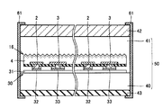
- FIG. 12 is a schematic cross-sectional view illustrating the process of sealing the back electrode type solar cells 16 installed on the wiring sheet 30.
- the sheet-like first resin layer 40, the sheet-like second resin layer 41, and the transparent protective substrate 42 are arranged in this order.
- the sheet-like first resin layer 40 and the back surface protection sheet 43 are arranged in this order from the wiring sheet 30 side.
- the back surface electrode type solar cell 16 sealed in the sealing material 50 is not limited to plural, and may be single.
- the sheet resistance of the n + layer 6 as the light-receiving surface diffusion layer of the back electrode type solar cell 16 is set to 40 ⁇ / ⁇ or more and 80 ⁇ / ⁇ or less, and the back electrode type solar cell 16
- the volume resistivity at 85 ° C. of the sealing material (second resin layer 41) provided on the light receiving surface is set to 1 ⁇ 10 16 ⁇ ⁇ cm or less.
- the sheet resistance of the n + layer 6 as the light-receiving surface diffusion layer of the back electrode type solar cell 16 is less than 40 ⁇ / ⁇ , recombination in the n + layer 6 increases, so that the back electrode type The output of the solar battery cell 16 itself decreases.
- the sheet resistance of the n + layer 6 is higher than 80 ⁇ / ⁇ , a large potential difference is generated between the back electrode type solar cell 16 and the frame 61, and moisture or the like is present on the surface of the transparent protective substrate 42. If accumulated, charge accumulates in the light-receiving surface passivation film 8 of the back electrode type solar cell 16, and the function of the n + layer 6 as an FSF (Front Surface Field) deteriorates.
- FSF Front Surface Field
- the volume resistivity at 45 ° C. to 85 ° C. is as high as 1 ⁇ 10 16 ⁇ ⁇ cm or more. Since it is possible to suppress a decrease in output due to PID or the like without using a special sealing material, the choice of the sealing material provided on the light-receiving surface of the back electrode type solar cell 16 as compared with the prior art It can be expanded and long-term reliability can be ensured.
- a special high resistance material having a volume resistivity of 1 ⁇ 10 16 ⁇ ⁇ cm or more at 45 ° C. to 85 ° C.
- the manufacturing cost of the solar cell module can be kept low.
- the volume resistivity at 45 ° C. to 85 ° C. is as high as 1 ⁇ 10 16 ⁇ ⁇ cm or more, Since it is not necessary to use a sealing material that is very difficult to handle, the manufacturing efficiency of the solar cell module can be improved.
- FIG. 14 shows a schematic cross-sectional view of a modification of the solar cell of the second embodiment.
- the sealing material 50 that seals the back electrode type solar cell 16 is the second resin on the light receiving surface of the back electrode type solar cell 16. It consists of the laminated body of the layer 41 and the 1st resin layer 40 on the wiring sheet 30, It is characterized by the above-mentioned.
- the sheet resistance of n + layer 6 as the light-receiving surface diffusion layer of back electrode type solar cell 16 is set to 40 ⁇ / ⁇ or more and 80 ⁇ / ⁇ or less. Therefore, a sealing material (second resin layer 41) having a volume resistivity of 1 ⁇ 10 16 ⁇ ⁇ cm or less at 85 ° C. is used as the sealing material provided on the light receiving surface of the back electrode type solar cell 16. be able to.
- the modification of the solar cell of Embodiment 2 shown in FIG. 14 can also be made into a solar cell which can ensure long-term reliability, without using a special and expensive sealing material.
- FIG. 15 is a schematic cross-sectional view of another modification of the solar cell of the second embodiment.
- the sealing material for sealing back electrode type solar battery cell 16 is formed of sealing material 52 made of a single layer of olefin resin. It is characterized by that.
- the sheet resistance of the n + layer 6 as the light-receiving surface diffusion layer of the back electrode type solar cell 16 is 40 ⁇ / ⁇ or more and 80 ⁇ / ⁇ or less. Therefore, as a sealing material provided on the light receiving surface of the back electrode type solar cell 16, a sealing material 52 made of a single layer of an olefin resin having a volume resistivity at 85 ° C. of 1 ⁇ 10 16 ⁇ ⁇ cm or less. Can be used. Thereby, the other modification of the solar cell of Embodiment 1 shown in FIG. 15 can also be set as the solar cell which can ensure long-term reliability, without using a special and expensive sealing material.
- the back electrodes of Examples 1 to 5 and Comparative Examples 1 to 3 were manufactured by the same method as that for manufacturing the back electrode type solar battery cell of Embodiment 1 shown in FIGS. 3 (a) to 3 (i).
- Type solar cell 1 was produced.
- the back electrodes of Examples 6 to 8 and Comparative Examples 4 to 6 were produced by the same method as the method of manufacturing the back electrode type solar cell of Embodiment 2 shown in FIGS. 11 (a) to 11 (k).
- Type solar cell 16 was produced.
- the back electrode type solar cells 1 of Examples 1 to 5 and Comparative Examples 1 to 3 are composed of phosphorus pentoxide, tetraisopropyl titanate, and isopropyl alcohol used for forming the n + layer 6 that is the light receiving surface diffusion layer. As shown in Table 1, by adjusting the phosphorous concentration in the solution 27 containing N, the sheet resistance of the n + layer 6 was changed, and the same conditions and the same method were used.
- the back electrode type solar cells 16 of Examples 6 to 8 and Comparative Examples 4 to 6 also contain phosphorus pentoxide, tetraisopropyl titanate, and isopropyl alcohol used for forming the n + layer 6 that is the light receiving surface diffusion layer. As shown in Table 1, by adjusting the phosphorous concentration in the solution 27 to be contained, it was produced under the same conditions and the same method except that the sheet resistance of the n + layer 6 was changed.
- the sheet resistance values of the light-receiving surface diffusion layers of the back electrode type solar cells of Examples 1 to 8 and Comparative Examples 1 to 6 shown in Table 1 were determined using Examples 1 to 8 and Mirror wafer.
- the sample was formed up to the n + layer 6 under the same conditions and in the same manner as the back electrode type solar cells of Comparative Examples 1 to 6, and then the sample with the surface of the n + layer 6 exposed was prepared.
- the value measured by the four-probe method at room temperature (25 ° C.) was used.
- the back electrode type solar cells 1 of Examples 1 to 8 and Comparative Examples 1 to 6 were respectively installed on the wiring sheet 30, and a transparent protective substrate 42 made of glass,
- the volume resistivity at 85 ° C. was adjusted to be different as shown in Table 1 by changing the content of the additive between the back protective sheet 43 made of a PET film on which an aluminum film was deposited. It sealed in the sealing material 52 which consists of a single layer of an olefin resin.
- the volume resistivity values at 85 ° C. of the sealing materials used for sealing the back electrode type solar cells of Examples 1 to 8 and Comparative Examples 1 to 6 shown in Table 1 are as follows. Asked.
- a copper foil having a diameter of 5 cm On a Teflon (registered trademark) sheet, a copper foil having a diameter of 5 cm, a sealing material having a length of about 10 cm ⁇ width of about 10 cm ⁇ thickness of about 0.04 cm, a copper foil having a diameter of 5 cm, and a Teflon (registered trademark) sheet
- the encapsulating material was cured by applying the pressure under the same conditions as when the back electrode type solar cells were sealed, and then heating.
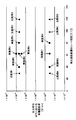
- FIG. 17 shows the relationship between the sheet resistance of the light-receiving surface diffusion layer of the back electrode type solar cells of Examples 1 to 8 and Comparative Examples 1 to 6 and the volume resistivity at 85 ° C. of the sealing material.
- the pseudo negative electrode 51 is grounded, and the back electrode type solar cell in an environment of 85 ° C.
- a pseudo negative electrode ground test was performed in which a voltage of 600 V was applied between 1 and the pseudo negative electrode 51 and left for 20 hours.
- Cell output change rate [%] 100 ⁇ ⁇ (cell output after pseudo negative grounding test) ⁇ (cell output before pseudo negative grounding test) ⁇ / (cell output before pseudo negative grounding test) (I)
- the sheet resistance of the light-receiving surface diffusion layer shown in Table 1 the volume resistivity of the sealing material at 85 ° C., the cell output before and after the pseudo negative electrode grounding test, and the output change rate are average values of n number of 5, respectively. is there.
- the sheet resistance of the light-receiving surface diffusion layer is 40 ⁇ / ⁇ or more and 80 ⁇ / ⁇ or less, and the volume resistivity at 85 ° C. of the sealing material is 1 ⁇ 10 16 ⁇ ⁇ cm or less All of the solar cells of ⁇ 8 were evaluated as A, and the solar cells of Comparative Examples 1-6 were all evaluated as B.
- the solar cells of Examples 1 to 8 can make the output of the back electrode type solar cell 1 itself higher than the solar cells of Comparative Examples 1 to 6, and the back electrode type solar cell. It was confirmed that a decrease in the output of the solar cell including 1 can be stably and sufficiently suppressed.
- the solar cells of Examples 1 to 5 in which the volume resistivity at 85 ° C. of the encapsulant is 2.8 ⁇ 10 15 ⁇ ⁇ cm or more and 5.1 ⁇ 10 15 ⁇ ⁇ cm or less the back electrode type solar cell It was confirmed that the decrease in the output of the solar battery including the battery cell 1 can be more stably and sufficiently suppressed.
- the solar cells of Examples 1 to 8 can ensure long-term reliability without using a special and expensive sealing material.
- the present invention comprises a back electrode type solar cell and a sealing material provided on the light receiving surface of the back electrode type solar cell, the back electrode type solar cell comprising a first conductivity type semiconductor substrate, A first conductive type light receiving surface diffusion layer provided on the light receiving surface side surface of the semiconductor substrate, and a first conductive type impurity diffusion layer and a second conductive type provided on the surface opposite to the light receiving surface side of the semiconductor substrate.
- the sheet resistance of the light-receiving surface diffusion layer is 40 ⁇ / ⁇ or more and 80 ⁇ / ⁇ or less, and the volume resistivity at 85 ° C. of the sealing material is 1 ⁇ 10 16 ⁇ ⁇ cm or less. It is a solar cell. With such a configuration, long-term reliability of the solar cell can be ensured without using a special and expensive sealing material.
- the light-receiving surface diffusion layer may be formed by applying a heat treatment after applying a solution containing a compound containing a first conductivity type impurity, titanium alkoxide, and alcohol. preferable. With such a configuration, the long-term reliability of the solar cell can be ensured without using a special and expensive sealing material.
- the sealing material is preferably composed of a single layer of olefin resin. Even if it is set as such a structure, long-term reliability of a solar cell can be ensured, without using a special and expensive sealing material.
- the sealing material includes a first resin layer on the light receiving surface of the back electrode type solar cell and a second resin layer on the first resin layer, and the second resin layer.
- the resin layer is preferably made of an olefin resin. Even if it is set as such a structure, long-term reliability of a solar cell can be ensured, without using a special and expensive sealing material.
- the volume resistivity of the encapsulant at 85 ° C. is preferably 1 ⁇ 10 12 ⁇ ⁇ cm or more and 1 ⁇ 10 16 ⁇ ⁇ cm or less.
- the volume resistivity of the sealing material is preferably 1 ⁇ 10 15 ⁇ ⁇ cm or more and 1 ⁇ 10 16 ⁇ ⁇ cm or less.
- the volume resistivity of the sealing material is preferably 2.8 ⁇ 10 15 ⁇ ⁇ cm or more and 5.1 ⁇ 10 15 ⁇ ⁇ cm or less.
- the present invention is a method for producing the solar cell according to any one of the above, wherein a compound containing an impurity of the first conductivity type, titanium alkoxide, alcohol on the light receiving surface side surface of the semiconductor substrate, And a step of forming a light-receiving surface diffusion layer and an antireflection film by applying a heat treatment after applying a solution containing, and a step of sealing the back electrode type solar cell with a sealing material. It is a manufacturing method. With such a configuration, long-term reliability of the solar cell can be ensured without using a special and expensive sealing material.
- the present invention can be used for a solar cell, and in particular, a back electrode type solar cell with a wiring sheet in which a plurality of back electrode type solar cells are connected in series and / or in parallel by wiring of a wiring sheet. It can use suitably for the solar cell module sealed in.
Abstract
L'invention concerne une cellule solaire qui permet d'obtenir une fiabilité à long terme sans utiliser un matériau de scellage spécial et coûteux. Cette cellule solaire comprend une couche de diffusion de surface de réception de lumière qui possède une résistance de feuille d'entre 40 Ω/□ et 80 Ω/□ (inclus) et un matériau de scellage qui possède une résistivité volumique à 85°C de 1 × 10¹⁶ Ω·cm ou moins.
Applications Claiming Priority (2)
| Application Number | Priority Date | Filing Date | Title |
|---|---|---|---|
| JP2013058244A JP2014183271A (ja) | 2013-03-21 | 2013-03-21 | 太陽電池 |
| JP2013-058244 | 2013-03-21 |
Publications (1)
| Publication Number | Publication Date |
|---|---|
| WO2014148065A1 true WO2014148065A1 (fr) | 2014-09-25 |
Family
ID=51579762
Family Applications (1)
| Application Number | Title | Priority Date | Filing Date |
|---|---|---|---|
| PCT/JP2014/050102 WO2014148065A1 (fr) | 2013-03-21 | 2014-01-08 | Cellule solaire |
Country Status (2)
| Country | Link |
|---|---|
| JP (1) | JP2014183271A (fr) |
| WO (1) | WO2014148065A1 (fr) |
Citations (5)
| Publication number | Priority date | Publication date | Assignee | Title |
|---|---|---|---|---|
| JP2010192909A (ja) * | 2004-04-28 | 2010-09-02 | Nakajima Glass Co Inc | 太陽電池モジュールの製造方法 |
| WO2011093360A1 (fr) * | 2010-02-01 | 2011-08-04 | シャープ株式会社 | Cellule solaire de type à électrode arrière, module de ladite cellule solaire, et procédé de fabrication de ladite cellule solaire |
| JP5016153B2 (ja) * | 2010-10-08 | 2012-09-05 | 三井化学株式会社 | 太陽電池封止材および太陽電池モジュール |
| JP2012209462A (ja) * | 2011-03-30 | 2012-10-25 | Lintec Corp | 太陽電池用保護シートおよびその製造方法、ならびに太陽電池モジュール |
| JP2012212948A (ja) * | 2012-08-09 | 2012-11-01 | Sharp Corp | 太陽電池モジュール |
-
2013
- 2013-03-21 JP JP2013058244A patent/JP2014183271A/ja active Pending
-
2014
- 2014-01-08 WO PCT/JP2014/050102 patent/WO2014148065A1/fr active Application Filing
Patent Citations (5)
| Publication number | Priority date | Publication date | Assignee | Title |
|---|---|---|---|---|
| JP2010192909A (ja) * | 2004-04-28 | 2010-09-02 | Nakajima Glass Co Inc | 太陽電池モジュールの製造方法 |
| WO2011093360A1 (fr) * | 2010-02-01 | 2011-08-04 | シャープ株式会社 | Cellule solaire de type à électrode arrière, module de ladite cellule solaire, et procédé de fabrication de ladite cellule solaire |
| JP5016153B2 (ja) * | 2010-10-08 | 2012-09-05 | 三井化学株式会社 | 太陽電池封止材および太陽電池モジュール |
| JP2012209462A (ja) * | 2011-03-30 | 2012-10-25 | Lintec Corp | 太陽電池用保護シートおよびその製造方法、ならびに太陽電池モジュール |
| JP2012212948A (ja) * | 2012-08-09 | 2012-11-01 | Sharp Corp | 太陽電池モジュール |
Also Published As
| Publication number | Publication date |
|---|---|
| JP2014183271A (ja) | 2014-09-29 |
Similar Documents
| Publication | Publication Date | Title |
|---|---|---|
| US9929294B2 (en) | Photoelectric conversion device, manufacturing method thereof, and photoelectric conversion module | |
| JP5258325B2 (ja) | 太陽電池モジュール | |
| EP2538447B1 (fr) | Cellule solaire et son procédé de fabrication | |
| EP2980858B1 (fr) | Procede de fabrication d'une cellule solaire | |
| JP2017508294A (ja) | 太陽電池の背面における導電性ポリマー/Si界面 | |
| JP2008270743A5 (fr) | ||
| JP4578123B2 (ja) | 太陽電池モジュール | |
| JP2013513964A (ja) | 裏面接点・ヘテロ接合太陽電池 | |
| US20130269774A1 (en) | Electrode of solar cell | |
| TWI424582B (zh) | 太陽能電池的製造方法 | |
| TW201417318A (zh) | 太陽能電池及其太陽能電池模組 | |
| WO2011024587A1 (fr) | Pâte électroconductrice, électrode pour dispositif à semi-conducteur, dispositif à semi-conducteur et processus de production de dispositif à semi-conducteur | |
| JP6207414B2 (ja) | 光起電力素子およびその製造方法 | |
| JP6114029B2 (ja) | 光起電力素子およびその製造方法 | |
| US20090308429A1 (en) | Thin-film solar module | |
| EP2806465B1 (fr) | Cellule solaire et son procédé de fabrication | |
| KR20110080663A (ko) | 태양광 발전장치 | |
| EP2618386B1 (fr) | Cellule solaire biface | |
| JP2013131698A (ja) | 配線シート付き太陽電池セル、太陽電池モジュールおよび太陽電池セルの製造方法 | |
| KR101223021B1 (ko) | 태양전지의 제조방법 및 태양전지 | |
| WO2014148065A1 (fr) | Cellule solaire | |
| JP6670808B2 (ja) | 高光電変換効率太陽電池、その製造方法、太陽電池モジュール及び太陽光発電システム | |
| CN109168322B (zh) | 太阳能电池组件以及太阳光发电系统 | |
| KR101406955B1 (ko) | 태양전지 및 그 제조방법 | |
| JP2019050329A (ja) | 太陽電池セルの製造方法 |
Legal Events
| Date | Code | Title | Description |
|---|---|---|---|
| 121 | Ep: the epo has been informed by wipo that ep was designated in this application |
Ref document number: 14769414 Country of ref document: EP Kind code of ref document: A1 |
|
| NENP | Non-entry into the national phase |
Ref country code: DE |
|
| 122 | Ep: pct application non-entry in european phase |
Ref document number: 14769414 Country of ref document: EP Kind code of ref document: A1 |