WO2014141592A1 - 光学部材およびその製造方法 - Google Patents
光学部材およびその製造方法 Download PDFInfo
- Publication number
- WO2014141592A1 WO2014141592A1 PCT/JP2014/000812 JP2014000812W WO2014141592A1 WO 2014141592 A1 WO2014141592 A1 WO 2014141592A1 JP 2014000812 W JP2014000812 W JP 2014000812W WO 2014141592 A1 WO2014141592 A1 WO 2014141592A1
- Authority
- WO
- WIPO (PCT)
- Prior art keywords
- shielding film
- film
- light shielding
- region
- light
- Prior art date
Links
Images


Classifications
-
- G—PHYSICS
- G02—OPTICS
- G02B—OPTICAL ELEMENTS, SYSTEMS OR APPARATUS
- G02B1/00—Optical elements characterised by the material of which they are made; Optical coatings for optical elements
- G02B1/10—Optical coatings produced by application to, or surface treatment of, optical elements
- G02B1/11—Anti-reflection coatings
-
- C—CHEMISTRY; METALLURGY
- C03—GLASS; MINERAL OR SLAG WOOL
- C03C—CHEMICAL COMPOSITION OF GLASSES, GLAZES OR VITREOUS ENAMELS; SURFACE TREATMENT OF GLASS; SURFACE TREATMENT OF FIBRES OR FILAMENTS MADE FROM GLASS, MINERALS OR SLAGS; JOINING GLASS TO GLASS OR OTHER MATERIALS
- C03C17/00—Surface treatment of glass, not in the form of fibres or filaments, by coating
- C03C17/34—Surface treatment of glass, not in the form of fibres or filaments, by coating with at least two coatings having different compositions
-
- G—PHYSICS
- G02—OPTICS
- G02B—OPTICAL ELEMENTS, SYSTEMS OR APPARATUS
- G02B1/00—Optical elements characterised by the material of which they are made; Optical coatings for optical elements
- G02B1/10—Optical coatings produced by application to, or surface treatment of, optical elements
- G02B1/11—Anti-reflection coatings
- G02B1/113—Anti-reflection coatings using inorganic layer materials only
-
- G—PHYSICS
- G02—OPTICS
- G02B—OPTICAL ELEMENTS, SYSTEMS OR APPARATUS
- G02B1/00—Optical elements characterised by the material of which they are made; Optical coatings for optical elements
- G02B1/10—Optical coatings produced by application to, or surface treatment of, optical elements
- G02B1/11—Anti-reflection coatings
- G02B1/118—Anti-reflection coatings having sub-optical wavelength surface structures designed to provide an enhanced transmittance, e.g. moth-eye structures
-
- G—PHYSICS
- G02—OPTICS
- G02B—OPTICAL ELEMENTS, SYSTEMS OR APPARATUS
- G02B1/00—Optical elements characterised by the material of which they are made; Optical coatings for optical elements
- G02B1/10—Optical coatings produced by application to, or surface treatment of, optical elements
- G02B1/12—Optical coatings produced by application to, or surface treatment of, optical elements by surface treatment, e.g. by irradiation
-
- G—PHYSICS
- G02—OPTICS
- G02B—OPTICAL ELEMENTS, SYSTEMS OR APPARATUS
- G02B5/00—Optical elements other than lenses
- G02B5/02—Diffusing elements; Afocal elements
- G02B5/0273—Diffusing elements; Afocal elements characterized by the use
- G02B5/0294—Diffusing elements; Afocal elements characterized by the use adapted to provide an additional optical effect, e.g. anti-reflection or filter
-
- C—CHEMISTRY; METALLURGY
- C03—GLASS; MINERAL OR SLAG WOOL
- C03C—CHEMICAL COMPOSITION OF GLASSES, GLAZES OR VITREOUS ENAMELS; SURFACE TREATMENT OF GLASS; SURFACE TREATMENT OF FIBRES OR FILAMENTS MADE FROM GLASS, MINERALS OR SLAGS; JOINING GLASS TO GLASS OR OTHER MATERIALS
- C03C2217/00—Coatings on glass
- C03C2217/70—Properties of coatings
- C03C2217/73—Anti-reflective coatings with specific characteristics
Definitions
- the present invention relates to an optical member and a method for manufacturing the same, and more particularly to an optical member provided with an antireflection film on its surface and a light shielding portion around the antireflection film and a method for manufacturing the same.
- an antireflection structure (antireflection film) is provided on the light incident surface in order to reduce the loss of transmitted light due to surface reflection. ing.
- Patent Document 1 discloses an optical member provided with a fine uneven film mainly composed of alumina as an antireflection structure.
- a method for forming a fine concavo-convex film mainly composed of aluminum oxide an aluminum oxide film is formed by a vacuum film formation method or a liquid phase method (sol-gel method), and then hydrothermal treatment such as water vapor treatment or hot water immersion treatment. Is known to obtain a plate-like crystal film (fine concavo-convex film) by boehmite the surface layer.
- a light-shielding film is provided on the non-light effective portion of the optical member in order to suppress generation of harmful light that causes flare, ghosts, and the like. Generally done.
- Patent Document 2 a protective film of at least one layer is formed on a base material, a light-shielding film is formed on a protective film formed on a non-light effective portion of an optical element, and a protection formed on a light effective portion
- An optical member in which a plate-like crystal film mainly composed of aluminum oxide having an uneven structure is formed on a film is disclosed.
- an optical member provided with an antireflection structure including a plate-like crystal film containing aluminum oxide as a main component and a light-shielding film provided in a non-light effective portion
- the present inventors have the following problems. I found out.
- the plate-like crystal film (fine concavo-convex film) containing aluminum oxide as a main component is fragile, and wiping and peeling processing (ultrasonic cleaning, chemical solution immersion, etc.) for redoing at the time of paint failure to form a light-shielding film ) Is not possible.
- an optical thin film such as an aluminum oxide film that becomes a fine concavo-convex film or a fine concavo-convex film when subjected to hydrothermal treatment may be adversely affected by the solvent of the light shielding film.
- an adverse effect of the solvent for example, an organic component contained in the solvent of the light-shielding film may be eluted into the warm water and reattached to the surface of the aluminum oxide film, thereby inhibiting the formation of a fine uneven structure.
- the present invention has been made in view of the above circumstances, and an optical member manufacturing method and an optical member with few defects that can accurately and efficiently manufacture an optical member having an antireflection film and a light shielding film.
- the purpose is to provide.
- the first optical member manufacturing method of the present invention includes an antireflection film including a transparent fine concavo-convex film mainly composed of alumina hydrate in an optically effective region on the surface of a transparent substrate, A method for producing an optical member comprising a light shielding film in a region including a boundary portion adjacent to at least an optical effective region of an adjacent non-effective region, A first light shielding film forming step of forming the light shielding film only in a part of the region where the light shielding film is to be formed; Forming an optical thin film in a region where an antireflection film is to be formed with a hydrothermal treatment layer that is hydrothermally treated to form a fine concavo-convex film as an outermost layer; A second light-shielding film forming step of forming a light-shielding film over the entire region where the light-shielding film is not formed in the first light-shielding film forming step in the region where the light-shielding film is to be formed;
- the second method for producing an optical member of the present invention comprises an antireflection film including a transparent fine concavo-convex film mainly composed of hydrate of alumina in an optically effective area on the surface of a transparent substrate, and the optically effective area.
- a method for producing an optical member comprising a light shielding film in a region including a boundary portion adjacent to at least the optical effective region adjacent to the non-effective region, A first light shielding film forming step of forming the light shielding film only in a part of the region where the light shielding film is to be formed; Forming an optical thin film in a region where an antireflection film is to be formed with a hydrothermal treatment layer that is hydrothermally treated to form a fine concavo-convex film as an outermost layer; Forming a fine concavo-convex film in a region where an antireflection film is to be formed by hydrothermally treating the hydrothermal treatment layer; A second light-shielding film forming step for forming a light-shielding film over the entire region where the light-shielding film is not formed in the first light-shielding film forming step in the region where the light-shielding film is to be formed is performed in this order.
- the first light-shielding film forming step of the first and second optical member manufacturing methods of the present invention it is preferable to form a light-shielding film at the boundary between the non-effective area and the optically effective area.
- the light-shielding film is formed on the concavo-convex shape portion in the first light-shielding film forming step. Is preferably formed.
- optical thin film it is preferable to form the optical thin film by vapor deposition.
- the optically effective area where the antireflection film is formed may be a flat surface or a curved surface.
- a light shielding film by applying a coating material containing at least one of titanium black, carbon black, black resist, and black resin and a resin binder.
- a first optical member of the present invention includes an antireflection film including a transparent fine uneven film mainly composed of hydrate of alumina in an optically effective region on a surface of a transparent substrate, and is adjacent to the optically effective region.
- An optical member comprising a light-shielding film in an area including at least a boundary portion adjacent to the optical effective area of the effective area, It is characterized in that a part of the non-effective region has a part in which two light shielding films are stacked.
- the second optical member of the present invention is provided with an antireflection film including a transparent fine concavo-convex film mainly composed of alumina hydrate in the optically effective region on the surface of the transparent substrate, and is adjacent to the optically effective region.
- An optical member comprising a light-shielding film in an area including at least a boundary portion adjacent to the optical effective area of the effective area, A part of the ineffective area includes a light-shielding film, a portion in which an optical thin film different from the light-shielding film, and a light-shielding film are sequentially laminated.
- the above-mentioned part of the ineffective area includes an adjacent part to the optically effective area.
- the part of the ineffective region includes the concavo-convex shape portion.
- the optically effective area where the antireflection film is formed may be a flat surface or a curved surface.
- the light shielding film is preferably made of a material containing one or more of titanium black, carbon black, black resist, and black resin.
- the first and second optical member manufacturing methods of the present invention since the first light shielding part forming step is performed before the optical thin film forming step, correction such as wiping or peeling treatment is performed during the light shielding film forming step. Can be easily performed.
- the light shielding part forming step is divided into two times, and the amount of coating on the light shielding part region formed in the first light shielding part forming step is smaller than the entire amount of the light shielding part. In the process, generation of outgas during vacuum film formation can be suppressed. Therefore, contamination of the vacuum apparatus can be suppressed, and the occurrence of defects due to impurities mixed into the film formed in vacuum can be suppressed.
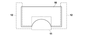
- Schematic cross section of transparent substrate Schematic cross-sectional view showing a region where an antireflection film is to be formed and a region where a light shielding film is to be formed in a transparent substrate
- Schematic cross-sectional view showing another example of a transparent substrate provided with a light shielding film formed in the first light shielding film forming step Schematic cross-sectional view showing a transparent substrate held by a holding component in the optical thin film process of the first embodiment
- An optical member manufactured by the manufacturing method of the present invention includes an antireflection film including a transparent fine concavo-convex film mainly composed of alumina hydrate in an optically effective region on the surface of a transparent substrate, and is adjacent to the optically effective region.
- An optical member comprising a light shielding film in a region including a boundary portion adjacent to at least the optical effective region of the non-effective region.
- the shape of the transparent substrate is not particularly limited as long as it is used in an optical apparatus such as a flat plate, a concave lens, and a convex lens, and a substrate composed of a combination of a curved surface and a flat surface having a positive or negative curvature is generally used.
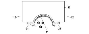
- a plano-concave lens 10 whose schematic cross-sectional view is shown in FIG. 1 will be described as an example as a transparent base material, but is not limited thereto.
- optical effective area and ineffective area in the optical member differ depending on the shape of the transparent substrate and the application.
- the concave surface area of the optically effective area of the plano-concave lens 10 is the antireflection film forming area 11 for forming the antireflection film, and the concave surface of the ineffective area is provided.
- the entire flat portion and the entire side surface of the surface are defined as a light shielding film forming region 12 for forming a light shielding film.
- the antireflection film forming region 11 and the light shielding film forming region 12 may be appropriately determined depending on the shape and application of the transparent substrate.
- the portion that becomes the optical effective region is generally composed of a combination of a curved surface and a flat surface having a positive or negative curvature.
- the region where the light-shielding film is to be formed does not include an optically effective region, and generally includes a lens side surface, a curved edge serving as an effective region, and the like.
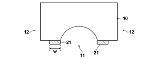
- the light shielding film 21 is formed only in a part of the light shielding film forming region 12.
- the first light-shielding film forming step it is desirable that the first light-shielding film is formed at a boundary portion adjacent to an optically effective region where a coating error is likely to occur, or at a portion having a complicated uneven shape.
- wiping for correction, ultrasonic cleaning processing, chemical solution immersion processing (caustic soda solution, etc.) occurs. Since this process has a significant adverse effect on the optical thin film and the fine concavo-convex film, the light-shielding film forming process is performed before forming the optical thin film in a region where a coating error is likely to occur.
- FIG. 3 shows a state in which the light shielding film 21 is formed at the boundary portion adjacent to the reflection film forming effect area 11 in the light shielding film forming area 12.
- the transparent substrate 10 having the concavo-convex portion 14 in the light-shielding film forming region 12 when using the transparent substrate 10 having the concavo-convex portion 14 in the light-shielding film forming region 12, the light-shielding film 21 is formed on the concavo-convex portion 14 in the first light-shielding film forming step. It is preferable.
- the concavo-convex shape portion 14 provided on the transparent substrate is a mechanical part when the optical member is incorporated in an optical device or the like, for example, specifically, fixing and preventing rotation of the lens assembled in the lens barrel. For fixing the optical filter to the turret.
- the range in which the light-shielding film at the boundary portion of the optical effective area of the optical element is formed is small.
- the lower limit of the light shielding film formation region (formation width) at this time is limited by the positional accuracy of the means for forming the light shielding film. For example, in the case where corner painting is performed by a person's hand using a brush, it depends on the skill of the person who paints, and in the case where it is mechanically performed by a stamper or the like, it depends on the positional accuracy of the stamper used.
- the formation width w of the light shielding film is preferably 10 mm or less. More preferably, it is preferably 5 mm or less, 2 mm or less, and further preferably 1 mm or less. However, when it is performed by a human hand using a brush, the lower limit is about 1 mm depending on individual skills.
- the range in which the light shielding film is formed can be 0.1 mm.
- the light shielding film is required to be at least opaque with respect to the light used, and is made of a material that substantially absorbs the light having the used wavelength without reflecting it.
- a black material that can form an optical light shielding portion is used. Note that the black material must be insoluble in water in order to perform heat treatment in a later step.
- a material made of any of titanium black, carbon black, black resist, black resin and a resin binder is used.
- an optical thin film is formed in the region where the antireflection film is to be formed, with the water-heat-treated layer that is hydrothermally processed to become a fine uneven film as the outermost layer.
- one or more optical thin films having a water-heat-treated layer containing an aluminum element as the outermost layer are formed.
- the number, material, and film thickness of the thin film layer are selected depending on the material and film thickness having a refractive index that provides suitable antireflection performance by the fine uneven film formed by hydrothermal treatment of the outermost layer.
- the refractive index of the fine concavo-convex film and the base material are greatly different, the reflectance is greatly reduced when an optical thin film having a refractive index smaller than that of the base material is formed on the base material.
- oxides, nitrides, oxynitrides, fluorides, and the like of elements selected from silicon, titanium, zircon, zinc, magnesium, and gallium are known.
- materials that can easily adjust the refractive index and obtain particularly suitable performance include silicon oxide and silicon oxynitride.
- the outermost layer as the water-heat-treated layer is assumed to contain an aluminum element. Preferably, it contains at least one material selected from aluminum, aluminum oxide, aluminum oxynitride, and aluminum nitride.
- the film forming method can be a batch type, and vapor phase film forming for improving productivity is preferable.
- a known vapor deposition method such as vacuum deposition, plasma sputtering, electron cyclotron sputtering, or ion plating can be used.
- the formation range of the optical thin film is at least a region where the antireflection film is to be formed, but may be formed over a part or the whole of the light shielding film formed in the first light shielding film forming step.
- film formation is performed by holding the transparent base material 10 in a state where the formation region of the optical thin film is exposed by the vacuum film forming holding part 35.
- the formation range of the optical thin film may be limited not only by masking with the holding component but also by masking with a separate mask means.
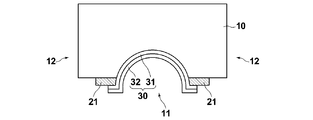
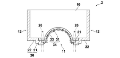
- the optical thin film forming step for example, as schematically shown in FIG. 6, on the antireflection film forming region 11 and a part of the light shielding film 21 formed in the first light shielding film forming step at the boundary adjacent thereto.
- the optical thin film 30 is formed.
- the optical thin film 30 is composed of two layers 31 and 32, and the hydrothermally treated layer 32 is formed as the outermost layer.
- the light shielding film 22 is formed in the entire region where the light shielding film 21 is not formed in the first light shielding film forming step in the region 12 where the light shielding film is to be formed.
- the light-shielding film 22 may be formed again on the region where the light-shielding film 21 is formed in the first light-shielding film forming process so that there is no formation of the light-shielding film.
- the light shielding film may be formed on the optical thin film formed in the thin film forming process so that there is no formation of the light shielding film.
- the light shielding film material used in the second light shielding film forming step is the same as that used in the first light shielding film forming step. In general, the same material is used in the first and second light shielding film forming steps, but different materials may be used as long as they are the above-described materials.
- a fine uneven film is formed by hydrothermally treating the optical thin film.
- the hydrothermal treatment layer 32 provided on the outermost layer of the optical thin film 30 is subjected to hydrothermal treatment such as exposing the optical thin film to water vapor or immersing the transparent substrate together with warm water.
- the film 33 is formed (FIG. 8).
- a hydrothermally treated film containing aluminum is heated to 1 atm. It is known that a fine concavo-convex film is formed when immersed for more than a minute. As a condition for obtaining a good fine concavo-convex film, it is preferable to immerse in warm water of 70 ° C. or higher for 3 minutes or longer. There is no particular upper limit for the dipping time, but it is preferably 30 minutes or less because elution of aluminum hydroxide proceeds slightly. When exposed to water vapor, it is preferable to expose to water at 143 ° C. or higher for 60 minutes or longer.
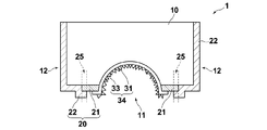
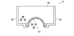
- the optically effective region on the surface of the transparent substrate 10 as shown in FIG. 8 is provided with the antireflection film 34 including the transparent fine concavo-convex film 33 mainly composed of alumina hydrate, and optically effective.
- the optical member 1 having the light shielding film 20 (21, 22) in the ineffective area adjacent to the antireflection film forming area 11 in the area can be obtained.
- the light shielding film 21 formed in the first light shielding film forming step and the light shielding film 22 formed in the second light shielding film forming step are partly in the ineffective region. There is an overlapping portion 25.
- the cross section of the light shielding films 21 and 22 is cross-sectioned by a scanning electron microscope (SEM) or the like. By observing, it can be confirmed that they are stacked.
- SEM scanning electron microscope
- hydrothermal treatment is performed on the optical thin film before the second light shielding film forming step.
- the details of the hydrothermal treatment are the same as in the case of the first embodiment.
- FIG. 9 a structure is obtained in which the transparent substrate 10 includes a partial light shielding film 21 and an antireflection film 34 including a fine uneven film 33 on the concave surface.
- a second light shielding film forming step is performed in which a light shielding film is formed in a region where the light shielding film 21 is not formed in the first light shielding film forming step in the light shielding film forming region 12.
- the second light shielding film forming step can be substantially the same as that of the first embodiment.
- the second light shielding film 22 may be formed so as to cover the end of the optical thin film 30 including the fine uneven film 33 formed on the first light shielding film 21. At the end of the optical thin film 30, the fine uneven film 33 is fragile, so it is broken by the pressure when the light shielding film 22 is applied, and only the layer 31 below the fine uneven film 33 remains.
- the optically effective region on the surface of the transparent substrate 10 as shown in FIG. 10 is provided with the antireflection film 34 including the transparent fine concavo-convex film 33 mainly composed of alumina hydrate, and is optically effective.
- An optical member 2 having a light shielding film 20 (21, 22) in an ineffective area adjacent to the antireflection film forming area 11 in the area can be obtained.
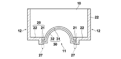
- the antireflection film forming region 11 on which the antireflection film is formed is a concave portion, and the entire flat surface portion on the concave surface around the concave portion and the entire side surface of the lens are formed on the light shielding film forming region 12. (See FIG. 2).
- a light-shielding film 21 made of carbon black and a resin binder was applied to the periphery of the optically effective region using a brush and formed with a width of 5 mm (see FIG. 3). The application was performed by fixing the transparent base material to the rotary stage with a vacuum chuck and rotating it slowly.
- the light shielding film 21 is formed only at the boundary portion adjacent to the effective region.
- the place where a coating film error is a concern depends on the lens shape. You may form in the other place which is not illustrated.
- the transparent base material 10 is held in the vacuum film-forming apparatus by the vacuum film-forming holding part 35 shown in FIG. 5, the silicon oxynitride thin film layer 31 is formed to a thickness of 90 nm by the reactive sputtering apparatus, and the alumina thin film layer 32 is subsequently formed. Was deposited to 40 nm.
- the silicon oxynitride thin film layer 31 and the alumina thin film layer 32 constitute the optical thin film 30.
- the vacuum film-forming holding component 35 is designed so as to mask a part of the light shielding film 21 formed in the first light shielding film forming step, and the optical thin film 30 is formed on a part of the light shielding film 21. Not to be.
- the silicon oxynitride thin film layer 31 and the alumina thin film layer 32 are formed as shown in FIG.
- the light shielding film 22 was formed in the same manner as in the first light shielding film forming step in the region where the light shielding film was not yet applied in the light shielding film forming region. At this time, the light-shielding film 22 was formed so as to overlap with a part of the light-shielding film 21 formed for the first time so as not to form a formation part (see FIG. 7).
- the transparent base material 10 on which the light-shielding films 20 (21, 22) and the optical thin film 30 are formed is immersed in warm water at 80 ° C. for 5 minutes, the outermost alumina thin film layer 32 becomes an aluminum hydroxide and becomes fine. It became the fine uneven
- the antireflection film forming region 11 good antireflection characteristics were obtained on the concave surface of the concave lens due to optical interference between the silicon oxynitride layer 31 and the fine concavo-convex film 33 formed by plate crystals.
- Example 1 an optically effective area on the surface of the transparent substrate 10 is provided with an antireflection film 34 including a transparent fine uneven film 33 mainly composed of hydrate of alumina.
- An optical member provided with a light shielding film 20 (21, 22) in an ineffective area adjacent to the antireflection film forming area 11 in the effective area, and in the first light shielding film forming step in a part of the ineffective area.
- Example 2 In the same manner as in Example 1, the light shielding film 21 was formed on the transparent substrate 10 in the first light shielding film forming step, and then the optical thin film 30 was formed. Thereafter, before performing the second light shielding film forming step, when the transparent base material 10 on which a part of the light shielding film 21 and the optical thin film 30 are formed is immersed in warm water of 80 ° C. for 5 minutes, the outermost alumina thin film layer 32 is formed. Becomes aluminum hydroxide and becomes a fine uneven film 33 made of fine plate crystals (see FIG. 9).
- a light shielding film 22 is formed in a region of the light shielding film forming region 12 where the light shielding film 21 is not yet applied by the same method as the first light shielding film forming step.
- the light shielding film 22 was formed so as to be overlapped with a part of the light shielding film 21 formed first so as not to form a formation part.
- Example 3 In the same manner as in Example 1, the light shielding film 21 was formed on the transparent substrate 10 in the first light shielding film forming step, and then the optical thin film 30 was formed. At this time, the optical thin film 30 was formed over the entire surface of the light shielding film 21. Next, the second light shielding film forming step is performed in the same manner as in the first embodiment. At this time, the silicon oxynitride thin film formed on the light shielding film 21 is formed so as to prevent the formation of the light shielding film. The light shielding film 22 was formed so as to overlap the layer 31 and part of the alumina thin film layer 32. In this way, as shown in FIG.
- the light shielding film 21 and the optical thin film 30 (the silicon oxynitride thin film layer 31 and the alumina thin film are formed on a part of the ineffective area adjacent to the optical effective area from the transparent substrate 10 side.
- a portion 27 in which the layer 32) and the light shielding film 22 are sequentially stacked is formed.
- Example 3 the optically effective area of the surface of the transparent substrate 10 is provided with an antireflection film 34 including a transparent fine uneven film 33 mainly composed of alumina hydrate, and optical.
- An optical member provided with a light shielding film 20 (21, 22) in an ineffective area adjacent to the antireflection film forming area 11 in the effective area, and in the first light shielding film forming step in a part of the ineffective area.
- An optical element 3 was obtained in which a portion 27 formed by laminating the light shielding film 21 and the optical thin film 30 to be formed and the light shielding film 22 formed in the second light shielding film forming step was obtained.
- Example 4 In the same manner as in Example 1, the light shielding film 21 was formed on the transparent substrate 10 in the first light shielding film forming step, and then the optical thin film 30 was formed. Thereafter, before performing the second light shielding film forming step, when the transparent base material 10 on which a part of the light shielding film 21 and the optical thin film 30 are formed is immersed in warm water of 80 ° C. for 5 minutes, the outermost alumina thin film layer 32 is formed. Became aluminum hydroxide and became a fine uneven film 33 made of fine plate crystals (see FIG. 9).
- the light shielding film is formed in the same manner as the first light shielding film formation in the region of the light shielding film forming region 12 where the light shielding film 21 is not formed by the first light shielding film forming step. 22 is formed.
- the light-shielding film 22 was formed so as to overlap a part of the silicon oxynitride thin film layer 31 and the fine uneven film 33 formed on the light-shielding film 21 so as to prevent the formation of the light-shielding film.
- the fine concavo-convex film 33 made of a plate crystal of aluminum hydroxide is destroyed by the pressure at the time of applying the light shielding film 22, and as shown in FIG.
- the layer 31, which is an optical thin film different from the light shielding films 21, 22, is formed between the light shielding films 21, 22, such as the light shielding film 21, the silicon oxynitride thin film layer 31, and the light shielding film 22 from the transparent substrate 10 side.
- a layered portion 26 is formed. At this time, in the effective region, as in Example 1, good antireflection characteristics were obtained.
- Example 4 an optically effective region on the surface of the transparent substrate 10 is provided with an antireflection film 34 including a transparent fine uneven film 33 mainly composed of alumina hydrate.
- An optical member provided with a light shielding film 20 (21, 22) in an ineffective area adjacent to the antireflection film forming area 11 in the effective area, and in the first light shielding film forming step in a part of the ineffective area.
- An optical element 2 was obtained in which a portion 31 of the light shielding film 21 and the optical thin film 30 to be formed and the portion 26 where the light shielding film 22 formed in the second light shielding film formation step overlaps were present.
Landscapes
- Physics & Mathematics (AREA)
- Optics & Photonics (AREA)
- General Physics & Mathematics (AREA)
- Chemical & Material Sciences (AREA)
- Chemical Kinetics & Catalysis (AREA)
- Geochemistry & Mineralogy (AREA)
- Materials Engineering (AREA)
- Organic Chemistry (AREA)
- General Chemical & Material Sciences (AREA)
- Life Sciences & Earth Sciences (AREA)
- Engineering & Computer Science (AREA)
- Inorganic Chemistry (AREA)
- Surface Treatment Of Optical Elements (AREA)
- Optical Elements Other Than Lenses (AREA)
Abstract
【課題】光学有効領域に反射防止膜を備え、その周囲に遮光膜を備えた光学部材を精度よく効率的に製造する。 【解決手段】透明基材(10)の遮光膜を形成すべき領域(12)の一部にのみ遮光膜(21)を形成する第1の遮光膜形成工程と、反射防止膜(34)を形成すべき領域(11)に、水熱処理されて微細凹凸膜(33)となる被水熱処理層(32)を最表層とする光学薄膜(30)を成膜する工程と、遮光膜を形成すべき領域(12)のうち、第1の遮光膜形成工程で遮光膜(21)が形成されていない領域全体に遮光膜(22)を形成する第2の遮光膜形成工程と、被水熱処理層(32)を水熱処理することにより、反射防止膜(34)を形成すべき領域(11)に微細凹凸膜(33)を形成する工程をこの順に行う。
Description
本発明は、光学部材およびその製造方法に関し、特には、その表面に反射防止膜を備え、さらに反射防止膜の周辺部に遮光部分を備えた光学部材およびその製造方法に関するものである。
従来、ガラス、プラスチックなどの透光性部材からなるレンズ(透明基材)においては、表面反射による透過光の損失を低減するために光入射面に反射防止構造体(反射防止膜)が設けられている。
可視光に対する反射防止構造体として、誘電体多層膜や、可視光の波長よりも短いピッチの微細凹凸構造体などが知られている(特許文献1、2など)。
特許文献1には、アルミナを主成分とする微細凹凸膜が反射防止構造体として備えられた光学部材が開示されている。酸化アルミニウムを主成分とする微細凹凸膜の形成方法としては、酸化アルミニウムの膜を真空成膜法、あるいは液相法(ゾルゲル法)により形成し、その後、水蒸気処理あるいは温水浸漬処理などの水熱処理を行うことにより、表層をベーマイト化して板状結晶膜(微細凹凸膜)を得る方法が知られている。
特許文献1には、アルミナを主成分とする微細凹凸膜が反射防止構造体として備えられた光学部材が開示されている。酸化アルミニウムを主成分とする微細凹凸膜の形成方法としては、酸化アルミニウムの膜を真空成膜法、あるいは液相法(ゾルゲル法)により形成し、その後、水蒸気処理あるいは温水浸漬処理などの水熱処理を行うことにより、表層をベーマイト化して板状結晶膜(微細凹凸膜)を得る方法が知られている。
一方、レンズなどの光学部材を用いて光学系を構成する際には、フレアやゴーストなどの原因となる有害光の発生を抑制するため、光学部材の非光線有効部に遮光膜を設けることが一般的に行われている。
特許文献2には、基材上に少なくとも1層の保護膜を形成し、光学素子の非光線有効部に形成された保護膜上に遮光膜を形成し、かつ光線有効部に形成された保護膜上に凹凸構造を有する酸化アルミニウムを主成分とする板状結晶膜を形成した光学部材が開示されている。
酸化アルミニウムを主成分とする板状結晶膜を備えた反射防止構造と、非光線有効部に設けられる遮光膜とを備えた光学部材を作製する上で、本発明者らは、下記の課題があることを見出した。
第1に、酸化アルミニウムを主成分とする板状結晶膜(微細凹凸膜)は脆く、遮光膜を形成するためのすみ塗り失敗時にやり直しのためのふき取りや剥離処理(超音波洗浄、薬液浸漬など)ができない。
第2に、酸化アルミニウム膜を真空成膜で形成する場合、真空成膜工程前にすみ塗り(遮光膜の形成)を行うと、真空成膜時に遮光膜材料からのアウトガスが生じ、真空装置を汚染したり、酸化アルミニウム膜に不純物が混入したりする等の欠陥が発生する恐れがある。
第3に、水熱処理が施されることにより微細凹凸膜となる酸化アルミニウム膜などの光学薄膜や微細凹凸膜は、遮光膜の溶剤により悪影響を受けることがある。溶剤による悪影響としては、例えば、遮光膜の溶剤に含まれる有機成分が温水中に溶出し、酸化アルミニウム膜表面に再付着することで微細凹凸構造の形成を阻害するなどが考えられる。
本発明は、上記事情に鑑みてなされたものであって、反射防止膜と遮光膜を備えた光学部材を精度よく効率的に製造することができる光学部材の製造方法および欠陥の少ない光学部材を提供することを目的とする。
本発明の第1の光学部材の製造方法は、透明基材の表面の光学有効領域にアルミナの水和物を主成分とする透明な微細凹凸膜を含む反射防止膜を備え、光学有効領域と隣接する非有効領域の少なくとも光学有効領域に隣接する境界部を含む領域に遮光膜を備えてなる光学部材の製造方法であって、
遮光膜を形成すべき領域の一部にのみ遮光膜を形成する第1の遮光膜形成工程と、
反射防止膜を形成すべき領域に、水熱処理されて微細凹凸膜となる被水熱処理層を最表層とする光学薄膜を成膜する工程と、
遮光膜を形成すべき領域のうち、第1の遮光膜形成工程で遮光膜が形成されていない領域全体に遮光膜を形成する第2の遮光膜形成工程と、
被水熱処理層を水熱処理することにより、反射防止膜を形成すべき領域に微細凹凸膜を形成する工程をこの順に行うことを特徴とする。
遮光膜を形成すべき領域の一部にのみ遮光膜を形成する第1の遮光膜形成工程と、
反射防止膜を形成すべき領域に、水熱処理されて微細凹凸膜となる被水熱処理層を最表層とする光学薄膜を成膜する工程と、
遮光膜を形成すべき領域のうち、第1の遮光膜形成工程で遮光膜が形成されていない領域全体に遮光膜を形成する第2の遮光膜形成工程と、
被水熱処理層を水熱処理することにより、反射防止膜を形成すべき領域に微細凹凸膜を形成する工程をこの順に行うことを特徴とする。
本発明の第2の光学部材の製造方法は、透明基材の表面の、光学有効領域にアルミナの水和物を主成分とする透明な微細凹凸膜を含む反射防止膜を備え、光学有効領域と隣接する非有効領域の少なくも光学有効領域に隣接する境界部を含む領域に遮光膜を備えてなる光学部材の製造方法であって、
遮光膜を形成すべき領域の一部にのみ遮光膜を形成する第1の遮光膜形成工程と、
反射防止膜を形成すべき領域に、水熱処理されて微細凹凸膜となる被水熱処理層を最表層とする光学薄膜を成膜する工程と、
被水熱処理層を水熱処理することにより、反射防止膜を形成すべき領域に微細凹凸膜を形成する工程と、
遮光膜を形成すべき領域のうち、第1の遮光膜形成工程で遮光膜が形成されていない領域全体に遮光膜を形成する第2の遮光膜形成工程をこの順に行うことを特徴とする。
遮光膜を形成すべき領域の一部にのみ遮光膜を形成する第1の遮光膜形成工程と、
反射防止膜を形成すべき領域に、水熱処理されて微細凹凸膜となる被水熱処理層を最表層とする光学薄膜を成膜する工程と、
被水熱処理層を水熱処理することにより、反射防止膜を形成すべき領域に微細凹凸膜を形成する工程と、
遮光膜を形成すべき領域のうち、第1の遮光膜形成工程で遮光膜が形成されていない領域全体に遮光膜を形成する第2の遮光膜形成工程をこの順に行うことを特徴とする。
本発明の第1および第2の光学部材の製造方法の第1の遮光膜形成工程においては、非有効領域の、光学有効領域と隣接する境界部に遮光膜を形成することが好ましい。
本発明の第1および第2の光学部材の製造方法は、透明基材が、非有効領域に凹凸形状部を有するものであるとき、第1の遮光膜形成工程において、凹凸形状部に遮光膜を形成することが好ましい。
光学薄膜を気相成膜により成膜することが好ましい。
反射防止膜が形成されている光学有効領域は平面であっても曲面であってもよい。
第1および第2の遮光膜形成工程において、チタンブラック、カーボンブラック、黒色レジスト、黒色樹脂のうちいずれか1つ以上と樹脂バインダを含む塗布材料を塗布して遮光膜を形成することが好ましい。
本発明の第1の光学部材は、透明基材の表面の光学有効領域にアルミナの水和物を主成分とする透明な微細凹凸膜を含む反射防止膜を備え、光学有効領域と隣接する非有効領域の少なくとも該光学有効領域に隣接する境界部を含む領域に遮光膜を備えてなる光学部材であって、
非有効領域の一部に、遮光膜が2層重ねて形成された部分を有していることを特徴とする。
非有効領域の一部に、遮光膜が2層重ねて形成された部分を有していることを特徴とする。
本発明の第2の光学部材は、透明基材の表面の光学有効領域にアルミナの水和物を主成分とする透明な微細凹凸膜を含む反射防止膜を備え、光学有効領域と隣接する非有効領域の少なくとも該光学有効領域に隣接する境界部を含む領域に遮光膜を備えてなる光学部材であって、
非有効領域の一部に、遮光膜、遮光膜とは異なる光学薄膜、遮光膜が順次積層されてなる部分を有していることを特徴とする。
非有効領域の一部に、遮光膜、遮光膜とは異なる光学薄膜、遮光膜が順次積層されてなる部分を有していることを特徴とする。
本発明の第1および第2の光学部材は、非有効領域の上記一部が、光学有効領域との隣接部を含むものであることが好ましい。
本発明の第1および第2の光学部材は、透明基材が、非有効領域に凹凸形状部を有するものであるとき、非有効領域の上記一部が、凹凸形状部を含むものであることが好ましい。
反射防止膜が形成されている光学有効領域は平面であっても曲面であってもよい。
遮光膜は、チタンブラック、カーボンブラック、黒色レジスト、黒色樹脂のうちいずれか1つ以上を含む材料からなることが好ましい。
本発明の第1および第2の光学部材の製造方法によれば、第1の遮光部形成工程は、光学薄膜の形成工程前に行うので、遮光膜形成工程中にふき取りや剥離処理などの修正を容易に行うことができる。一方で、遮光部形成工程を2回に分けており、第1の遮光部形成工程で形成する遮光部領域への塗布量は、遮光部全域よりも少ない塗布量となるため、光学薄膜の形成工程において、真空成膜を行う際のアウトガスの発生を抑制することができる。従って、真空装置の汚染を抑制すると共に、真空成膜される膜に不純物が混入し欠陥が生じることを抑制することができる。
また、光学薄膜の形成後もしく凹凸微細膜形成後には、第1の遮光形成工程で形成しなかった領域のみに遮光膜を形成すればよいため、第2の遮光膜形成工程は短時間で行うことができ、光学薄膜や凹凸微細膜への溶剤による悪影響を抑制することができる。
以下、図面を参照して本発明の実施形態を説明する。
本発明の製造方法により製造する光学部材は、透明基材の表面の光学有効領域にアルミナの水和物を主成分とする透明な微細凹凸膜を含む反射防止膜を備え、光学有効領域と隣接する非有効領域の少なくとも該光学有効領域に隣接する境界部を含む領域に遮光膜を備えてなる光学部材である。
透明基材の形状は特に限定なく、平板、凹レンズ、凸レンズなど光学装置において用いられるものであればよく、正または負の曲率を有する曲面と平面の組合せで構成された基材を一般的に用いる。以下の実施形態においては透明基材として図1に模式断面図を示す平凹レンズ10を例に挙げて説明するが、これに限るものではない。
透明基材の形状や、用途により光学部材における光学有効領域および非有効領域は異なる。なお、本発明の光学部材においてが、透明基材の表面に、反射防止膜が形成されていない光学有効領域や遮光膜が形成されていない非有効領域が存在しても構わない。
以下の実施形態においては、図2に示すように、平凹レンズ10の光学有効領域のうち凹面領域を、反射防止膜を形成する反射防止膜形成領域11とし、非有効領域のうち凹面を備えた面の平面部全域および側面全域を、遮光膜を形成する遮光膜形成領域12とする。反射防止膜形成領域11および遮光膜形成領域12は、透明基材の形状や用途により適宜定めればよい。光学的な有効領域となる部分は、一般に正または負の曲率をもつ曲面と平面の組み合わせで構成される。遮光膜を形成すべき領域(遮光膜形成領域12)には光学的な有効領域は含まれず、一般にレンズ側面や有効領域となる曲面の縁部などが含まれる。
「第1の実施形態の製造方法」
まず、本発明の第1の光学素子の製造方法に基づく第1の実施形態を説明する。図3~図7は本実施形態の製造工程を示す模式断面図である。
まず、本発明の第1の光学素子の製造方法に基づく第1の実施形態を説明する。図3~図7は本実施形態の製造工程を示す模式断面図である。
まず、第1の遮光膜形成工程として、図3に示すように、遮光膜形成領域12のうち一部にのみ遮光膜21を形成する。
第1の遮光膜形成工程においては、特に塗装ミスの起こりやすい光学的な有効領域に隣接する境界部や、複雑な凹凸形状を持つ部に形成することが望ましい。塗装ミスが起こった場合、修正のためのふき取りや超音波洗浄処理、薬液浸漬処理(苛性ソーダ溶液など)が発生する。この工程は光学薄膜や微細凹凸膜に著しい悪影響を与えるため、塗装ミスの起こりやすい領域への遮光膜形成処理を光学薄膜形成前に行うこととしている。
第1の遮光膜形成工程においては、特に塗装ミスの起こりやすい光学的な有効領域に隣接する境界部や、複雑な凹凸形状を持つ部に形成することが望ましい。塗装ミスが起こった場合、修正のためのふき取りや超音波洗浄処理、薬液浸漬処理(苛性ソーダ溶液など)が発生する。この工程は光学薄膜や微細凹凸膜に著しい悪影響を与えるため、塗装ミスの起こりやすい領域への遮光膜形成処理を光学薄膜形成前に行うこととしている。
図3においては、遮光膜形成領域12の反射膜形成効領域11と隣接する境界部に遮光膜21を形成している様子を示している。他方、図4に示すように、遮光膜形成領域12に凹凸形状部14を有する透明基材10を用いる場合、第1の遮光膜形成工程で、この凹凸形状部14に遮光膜21を形成することが好ましい。透明基材に設けられる凹凸形状部14は、例えば、光学部材が光学装置などに組み込まれる際の機構的な部分であり、具体的には、鏡筒に組み付けられたレンズの固定および回転防止のための固定溝や、光学フィルタをターレットに固定するときの割り等である。
なお、第1の遮光膜形成工程において、光学素子の光学有効領域の境界部の遮光膜を形成する範囲は小さい方が好ましい。なお、このときの遮光膜形成領域(形成幅)の下限は遮光膜を形成する手段の位置精度により制限される。例えば、筆を用い人の手によりすみ塗りが行われる場合には、塗る人の技能に依存し、スタンパなどにより機械的に行われる場合には、用いられるスタンパの位置精度に依存する。
境界部に遮光膜を形成する際、形成範囲は形成手段の位置精度以上であれば小さいほどよい。遮光膜の形成幅wは10mm以下とするのが好ましい。より好ましくは5mm以下、2mm以下、さらには1mm以下とすることが好ましいが、筆を用いて人の手で行う場合には、個人の技能によるが1mm程度が下限値となる。スタンパにより遮光膜の形成を行う場合、例えば、スタンパの位置精度が0.1mmであれば、遮光膜を形成する範囲は0.1mmとすることができる。
遮光膜は、少なくとも使用される光に対して不透明であることを要し、使用波長の光を反射することなくほぼ吸収する材料から構成される。具体的には、光学的な遮光部を形成できる黒色材料が用いられる。なお、後の工程において熱処理を行うため、黒色材料は水に不溶でなければならない。例えば、チタンブラック、カーボンブラック、黒色レジスト、黒色樹脂のいずれかと樹脂バインダからなる材料を用いる。
そして、第1の遮光膜形成工程の後、反射防止膜を形成すべき領域に、水熱処理されて微細凹凸膜となる被水熱処理層を最表層とする光学薄膜を成膜する。
この光学薄膜形成工程では、最表層にアルミニウム元素を含む被水熱処理層を備えた1層以上の光学薄膜が形成される。薄膜層の層数、材質および膜厚は、最表層を水熱処理し形成される微細凹凸膜により好適な反射防止性能が得られる屈折率をもつ材質および膜厚により選ばれる。
微細凹凸膜と基材の屈折率が大きく異なるような場合には、基材の屈折率より小さい屈折率を持つ光学薄膜を基材上に形成すると反射率が大きく低減されることが知られている。このような条件を満たす材料として、シリコン、チタン、ジルコン、亜鉛、マグネシウム、ガリウムから選ばれる元素の酸化物、窒化物、酸窒化物、弗化物などが知られている。屈折率調整が容易で、特に好適な性能を得られる材料としては、シリコン酸化物、シリコン酸窒化物が挙げられる。温水処理により微細凹凸膜を形成するため、被水熱処理層である最表層はアルミニウム元素を含むものとする。好ましくはアルミニウム、アルミニウム酸化物、アルミニウム酸窒化物、アルミニウム窒化物から選ばれる材料のうち少なくとも1種類を含むことが望ましい。
成膜方法はバッチ式が可能であり生産性を向上させる気相成膜が好ましい。例えば、真空蒸着、プラズマスパッタ、電子サイクロトロンスパッタ、イオンプレーティング等の公知の気相製膜法を利用することができる。
光学薄膜の形成範囲は、少なくとも反射防止膜を形成すべき領域であるが、第1の遮光膜形成工程で形成した遮光膜の一部または全域に亘って上にも形成されていてもよい。
真空成膜による光学薄膜の形成時には、例えば、図5に示すように、真空成膜用保持部品35により光学薄膜の形成領域を露出させた状態で透明基材10を保持させて成膜を行う。光学薄膜の形成範囲は、保持部品でマスクするのみならず別途のマスク手段によるマスキングを行って制限してもよい。
真空成膜による光学薄膜の形成時には、例えば、図5に示すように、真空成膜用保持部品35により光学薄膜の形成領域を露出させた状態で透明基材10を保持させて成膜を行う。光学薄膜の形成範囲は、保持部品でマスクするのみならず別途のマスク手段によるマスキングを行って制限してもよい。
光学薄膜の形成工程において、例えば、図6に模式的に示すように反射防止膜形成領域11およびそれに隣接する境界部の第1の遮光膜形成工程で形成された遮光膜21の一部上に光学薄膜30を形成する。本例では、光学薄膜30を2層31、32からなるものとしており、その最表層となる層として被水熱処理層32を形成している。
次に、第2の遮光膜形成工程として、遮光膜を形成すべき領域12のうち、第1の遮光膜形成工程で遮光膜21が形成されていない領域全体に遮光膜22を形成する。このとき、図7に示すように、遮光膜の形成モレがないように、第1の遮光膜形成工程で遮光膜21を形成した領域上に再度遮光膜22を重ねて形成しても良い。また、遮光膜の形成モレがないように、薄膜形成工程で形成した光学薄膜上に遮光膜を形成しても良い。
第2の遮光膜形成工程で用いられる遮光膜材料は、第1の遮光膜形成工程で用いられるものと同様である。一般には、第1および第2の遮光膜形成工程では、同一の材料を用いるが、上述した材料であれば、異なる材料を用いてもよい。
第2の遮光膜形成工程で用いられる遮光膜材料は、第1の遮光膜形成工程で用いられるものと同様である。一般には、第1および第2の遮光膜形成工程では、同一の材料を用いるが、上述した材料であれば、異なる材料を用いてもよい。
最後に、光学薄膜を水熱処理することにより、微細凹凸膜を形成する。光学薄膜を水蒸気に曝す、あるいは透明基材ごと温水に浸すなどの水熱処理を施すことにより、光学薄膜30の最表層に設けられている被水熱処理層32は、アルミナを主成分とする微細凹凸膜33となる(図8)。
非特許文献(山田 啓之、岡本常義:軽金属vol.21,No.9(1971)pp.597-605)に記載されるとおり、アルミニウムを含む被水熱処理膜を1気圧60℃以上の温水に1分以上浸漬すれば微細凹凸膜が形成されることが知られている。良好な微細凹凸膜を得るための条件としては、70℃以上の温水に3分以上浸漬することが好ましい。浸漬時間の上限は特に無いが、わずかながら水酸化アルミニウムの溶出が進行するため、30分以下とすることが好ましい。水蒸気に暴露する場合には、143℃以上の水蒸気に60分以上暴露することが好ましい。
以上の工程により、図8に示すような、透明基材10の表面の光学有効領域にアルミナの水和物を主成分とする透明な微細凹凸膜33を含む反射防止膜34を備え、光学有効領域の反射防止膜形成領域11と隣接する非有効領域に遮光膜20(21、22)を備えてなる光学部材1を得ることができる。
なお、図8に示す光学部材1においては、非有効領域の一部に、第1の遮光膜形成工程で形成される遮光膜21と第2の遮光膜形成工程で形成される遮光膜22が重なる部分25が存在する。なお、遮光膜21、22の積層箇所は、遮光膜21の塗布形成後、遮光膜が完全に完成した後に遮光膜22を塗布形成しているので、断面について走査型電子顕微鏡(SEM)等により観察することにより、積層して形成されていることを確認することができる。
なお、図8に示す光学部材1においては、非有効領域の一部に、第1の遮光膜形成工程で形成される遮光膜21と第2の遮光膜形成工程で形成される遮光膜22が重なる部分25が存在する。なお、遮光膜21、22の積層箇所は、遮光膜21の塗布形成後、遮光膜が完全に完成した後に遮光膜22を塗布形成しているので、断面について走査型電子顕微鏡(SEM)等により観察することにより、積層して形成されていることを確認することができる。
「第2の実施形態の製造方法」
次に、本発明の第2の光学素子の製造方法に基づく第2の実施形態を説明する。
第2の実施形態においても、まず、第1の遮光膜形成工程により一部の遮光膜21を形成し、その後、反射防止膜を形成すべき領域11に、水熱処理されて微細凹凸膜となる被水熱処理層32を最表層とする光学薄膜30を成膜する(図6参照)。これらの第1の遮光膜形成工程および光学薄膜形成工程までは第1の実施形態の場合と同様である。
次に、本発明の第2の光学素子の製造方法に基づく第2の実施形態を説明する。
第2の実施形態においても、まず、第1の遮光膜形成工程により一部の遮光膜21を形成し、その後、反射防止膜を形成すべき領域11に、水熱処理されて微細凹凸膜となる被水熱処理層32を最表層とする光学薄膜30を成膜する(図6参照)。これらの第1の遮光膜形成工程および光学薄膜形成工程までは第1の実施形態の場合と同様である。
その後、本実施形態においては、第2の遮光膜形成工程を行う前に光学薄膜に対する水熱処理を行う。水熱処理の詳細については第1の実施形態の場合と同様である。これにより、図9に示すように、透明基材10に、部分的な遮光膜21を備え、凹面に微細凹凸膜33を含む反射防止膜34を備えた構造が得られる。
その後、遮光膜形成領域12のうち第1の遮光膜形成工程で遮光膜21が形成されていない領域に遮光膜を形成する第2の遮光膜形成工程を行う。第2の遮光膜形成工程も第1の実施形態とほぼ同様とすることができる。なお、第1の遮光膜21上に形成された微細凹凸膜33を含む光学薄膜30の端部を覆うように第2の遮光膜22を形成してもよい。なお、光学薄膜30の端部では、微細凹凸膜33は脆いために遮光膜22の塗布の際の圧力で破壊され、微細凹凸膜33下層の層31のみが残る。
以上の工程により、図10に示すような、透明基材10の表面の光学有効領域にアルミナの水和物を主成分とする透明な微細凹凸膜33を含む反射防止膜34を備え、光学有効領域の反射防止膜形成領域11と隣接する非有効領域に遮光膜20(21、22)を備えてなる光学部材2を得ることができる。
なお、図10に示す光学部材2においては、非有効領域の一部に、透明基材10側から遮光膜21、光学薄膜30のうちの層31および遮光膜22が順次積層されてなる部分26が存在する。
なお、図10に示す光学部材2においては、非有効領域の一部に、透明基材10側から遮光膜21、光学薄膜30のうちの層31および遮光膜22が順次積層されてなる部分26が存在する。
以下、本発明のより具体的な光学部材の製造方法およびその製造方法で製造された光学部材の構成を実施例として説明する。
「実施例1」
径φ25mm、厚さ12.5mmの平凹レンズであって、凹部の曲率半径R=12mm、深さ4.5mmのランタンガラス製の透明基材を用意した(図1参照)。本実施例において反射防止膜が形成される反射防止膜形成領域11は凹部であり、その凹部周囲の凹面側の平面部全体とレンズの側面全体が、遮光膜が形成される遮光膜形成領域12である(図2参照)。
径φ25mm、厚さ12.5mmの平凹レンズであって、凹部の曲率半径R=12mm、深さ4.5mmのランタンガラス製の透明基材を用意した(図1参照)。本実施例において反射防止膜が形成される反射防止膜形成領域11は凹部であり、その凹部周囲の凹面側の平面部全体とレンズの側面全体が、遮光膜が形成される遮光膜形成領域12である(図2参照)。
まず、第1の遮光膜形成工程として、光学有効領域の周辺部にカーボンブラックと樹脂バインダからなる遮光膜21を、筆を用いて塗布し5mm幅で形成した(図3参照)。塗布は回転ステージに透明基材を真空チャックにより固定し、ゆっくり回転させることで行った。本実施例では第1の遮光膜形成工程において、有効領域と隣接する境界部にのみ遮光膜21を形成したが、塗膜ミスが懸念される場所はレンズ形状に依存するため、本実施例に図示しない他の場所に形成しても良い。
図5に示す真空成膜用保持部品35により真空成膜装置内に透明基材10を保持し、反応性スパッタ装置によりシリコン酸窒化物薄膜層31を90nm成膜し、続けてアルミナ薄膜層32を40nm成膜した。本例では、シリコン酸窒化物薄膜層31とアルミナ薄膜層32が光学薄膜30を構成している。ここで、真空成膜用保持部品35は第1の遮光膜形成工程により形成した遮光膜21の一部をマスクするように設計されており、遮光膜21の一部には光学薄膜30が形成されないようになっている。この結果、シリコン酸窒化物薄膜層31とアルミナ薄膜層32は図6に示されるように形成される。
次いで、第2の遮光膜形成工程として、遮光膜形成領域のうちまだ遮光膜が塗布されていない領域に第1の遮光膜形成工程の場合と同様の方法で遮光膜22を形成した。このとき、形成モレ部分ができないように1回目に形成した遮光膜21の一部に重ねて遮光膜22を形成した(図7参照)。
最後に、遮光膜20(21、22)および光学薄膜30が形成された透明基材10を80℃の温水に5分間浸漬すると、最表層のアルミナ薄膜層32はアルミニウム水酸化物となり、微細な板状結晶による微細凹凸膜33となった(図8参照)。反射防止膜形成領域11ではシリコン酸窒化物層31と板状結晶による微細凹凸膜33の光学干渉により、凹レンズの凹面では良好な反射防止特性が得られた。
本実施例1では、図8に示すように、透明基材10の表面の光学有効領にアルミナの水和物を主成分とする透明な微細凹凸膜33を含む反射防止膜34を備え、光学有効領域の反射防止膜形成領域11と隣接する非有効領域に遮光膜20(21、22)を備えてなる光学部材であって、非有効領域の一部に、第1の遮光膜形成工程で形成される遮光膜21と第2の遮光膜形成工程で形成される遮光膜22が重なる部分25が存在する光学素子1が得られた。
[実施例2]
実施例1と同様にして、透明基材10に対して第1の遮光膜形成工程において遮光膜21を形成し、次いで光学薄膜30を形成した。その後、第2の遮光膜形成工程を行う前に、一部の遮光膜21および光学薄膜30が形成された透明基材10を80℃の温水に5分間浸漬すると、最表層のアルミナ薄膜層32はアルミニウム水酸化物となり、微細な板状結晶による微細凹凸膜33となる(図9参照)。
実施例1と同様にして、透明基材10に対して第1の遮光膜形成工程において遮光膜21を形成し、次いで光学薄膜30を形成した。その後、第2の遮光膜形成工程を行う前に、一部の遮光膜21および光学薄膜30が形成された透明基材10を80℃の温水に5分間浸漬すると、最表層のアルミナ薄膜層32はアルミニウム水酸化物となり、微細な板状結晶による微細凹凸膜33となる(図9参照)。
その後、第2の遮光膜形成工程として、遮光膜形成領域12のうちまだ遮光膜21が塗布されていない領域に第1の遮光膜形成工程と同様の方法で遮光膜22を形成する。このとき、形成モレ部分ができないように最初に形成した遮光膜21の一部に重ねて遮光膜22を形成した。
本実施例2では、実施例1と同様の図8に示す、透明基材10の表面の光学有効領域にアルミナの水和物を主成分とする透明な微細凹凸膜33を含む反射防止膜34を備え、光学有効領域の反射防止膜形成領域11と隣接する非有効領域に遮光膜20(21、22)を備えてなる光学部材であって、非有効領域の一部に、第1の遮光膜形成工程で形成される遮光膜21と第2の遮光膜形成工程で形成される遮光膜22が重なる部分25が存在する光学素子1が得られた。
[実施例3]
実施例1と同様にして、透明基材10に対して第1の遮光膜形成工程において遮光膜21を形成し、次いで光学薄膜30を形成した。このとき、光学薄膜30を遮光膜21上全面に亘って形成した。次いで、実施例1の場合と同じく第2の遮光膜形成工程を行うが、このとき、遮光膜の形成モレ部分ができないように、遮光膜21の上に成膜されているシリコン酸窒化物薄膜層31とアルミナ薄膜層32の一部に重ねて遮光膜22を形成した。このようにすると、図11に示すように、光学有効領域に隣接する非有効領域の一部に、透明基材10側から遮光膜21、光学薄膜30(シリコン酸窒化物薄膜層31とアルミナ薄膜層32)、遮光膜22が順に積層された部分27が形成される。
実施例1と同様にして、透明基材10に対して第1の遮光膜形成工程において遮光膜21を形成し、次いで光学薄膜30を形成した。このとき、光学薄膜30を遮光膜21上全面に亘って形成した。次いで、実施例1の場合と同じく第2の遮光膜形成工程を行うが、このとき、遮光膜の形成モレ部分ができないように、遮光膜21の上に成膜されているシリコン酸窒化物薄膜層31とアルミナ薄膜層32の一部に重ねて遮光膜22を形成した。このようにすると、図11に示すように、光学有効領域に隣接する非有効領域の一部に、透明基材10側から遮光膜21、光学薄膜30(シリコン酸窒化物薄膜層31とアルミナ薄膜層32)、遮光膜22が順に積層された部分27が形成される。
最後に、図11に示す透明基材10を80℃の温水に5分間浸漬すると、光学薄膜30の最表層のアルミナ薄膜層32はアルミニウム水酸化物となり、微細な板状結晶による凹凸膜33となった(図12参照)。このときも有効領域では実施例1と同様に、良好な反射防止特性を得られた。
本実施例3では、図12に示すように、透明基材10の表面の光学有効領域にアルミナの水和物を主成分とする透明な微細凹凸膜33を含む反射防止膜34を備え、光学有効領域の反射防止膜形成領域11と隣接する非有効領域に遮光膜20(21、22)を備えてなる光学部材であって、非有効領域の一部に、第1の遮光膜形成工程で形成される遮光膜21と光学薄膜30と、第2の遮光膜形成工程で形成される遮光膜22が積層されてなる部分27が存在する光学素子3が得られた。
[実施例4]
実施例1と同様にして、透明基材10に対して第1の遮光膜形成工程において遮光膜21を形成し、次いで光学薄膜30を形成した。その後、第2の遮光膜形成工程を行う前に、一部の遮光膜21および光学薄膜30が形成された透明基材10を80℃の温水に5分間浸漬すると、最表層のアルミナ薄膜層32はアルミニウム水酸化物となり、微細な板状結晶による微細凹凸膜33となった(図9参照)。
実施例1と同様にして、透明基材10に対して第1の遮光膜形成工程において遮光膜21を形成し、次いで光学薄膜30を形成した。その後、第2の遮光膜形成工程を行う前に、一部の遮光膜21および光学薄膜30が形成された透明基材10を80℃の温水に5分間浸漬すると、最表層のアルミナ薄膜層32はアルミニウム水酸化物となり、微細な板状結晶による微細凹凸膜33となった(図9参照)。
最後に、第2の遮光膜形成工程として、遮光膜形成領域12のうち第1の遮光膜形成工程により遮光膜21が形成されていない領域に第1の遮光膜形成と同様の方法で遮光膜22を形成する。このとき、遮光膜の形成モレ部分ができないように、遮光膜21の上に成膜されているシリコン酸窒化物薄膜層31と微細凹凸膜33の一部に重ねて遮光膜22を形成した。このようにすると、アルミニウム水酸化物の板状結晶からなる微細凹凸膜33は遮光膜22の塗布時の圧力で破壊され、図10に示すように、光学有効領域に隣接する非有効領域の一部に、透明基材10側から遮光膜21、シリコン酸窒化物薄膜層31、遮光膜22のように、遮光膜21、22間に遮光膜21、22とは異なる光学薄膜である層31が積層されてなる部分26が形成される。このときも有効領域では実施例1と同様に、良好な反射防止特性を得られた。
本実施例4では、図10に示すように、透明基材10の表面の光学有効領域にアルミナの水和物を主成分とする透明な微細凹凸膜33を含む反射防止膜34を備え、光学有効領域の反射防止膜形成領域11と隣接する非有効領域に遮光膜20(21、22)を備えてなる光学部材であって、非有効領域の一部に、第1の遮光膜形成工程で形成される遮光膜21と光学薄膜30のうちの1層31と、第2の遮光膜形成工程で形成される遮光膜22が重なる部分26が存在する光学素子2が得られた。
Claims (13)
- 透明基材の表面の光学有効領域にアルミナの水和物を主成分とする透明な微細凹凸膜を含む反射防止膜を備え、該光学有効領域と隣接する非有効領域の少なくとも該光学有効領域に隣接する境界部を含む領域に遮光膜を備えてなる光学部材の製造方法であって、
前記遮光膜を形成すべき領域の一部にのみ前記遮光膜を形成する第1の遮光膜形成工程と、
前記反射防止膜を形成すべき領域に、水熱処理されて微細凹凸膜となる被水熱処理層を最表層とする光学薄膜を成膜する工程と、
前記遮光膜を形成すべき領域のうち、前記第1の遮光膜形成工程で前記遮光膜が形成されていない領域全体に前記遮光膜を形成する第2の遮光膜形成工程と、
前記被水熱処理層を水熱処理することにより、前記反射防止膜を形成すべき領域に前記微細凹凸膜を形成する工程をこの順に行うことを特徴とする光学部材の製造方法。 - 透明基材の表面の、光学有効領域にアルミナの水和物を主成分とする透明な微細凹凸膜を含む反射防止膜を備え、該光学有効領域と隣接する非有効領域の少なくも該光学有効領域に隣接する境界部を含む領域に遮光膜を備えてなる光学部材の製造方法であって、
前記遮光膜を形成すべき領域の一部にのみ前記遮光膜を形成する第1の遮光膜形成工程と、
前記反射防止膜を形成すべき領域に、水熱処理されて微細凹凸膜となる被水熱処理層を最表層とする光学薄膜を成膜する工程と、
前記被水熱処理層を水熱処理することにより、前記反射防止膜を形成すべき領域に前記微細凹凸膜を形成する工程と、
前記遮光膜を形成すべき領域のうち、前記第1の遮光膜形成工程で前記遮光膜が形成されていない領域全体に前記遮光膜を形成する第2の遮光膜形成工程をこの順に行うことを特徴とする光学部材の製造方法。 - 前記第1の遮光膜形成工程において、前記非有効領域の前記境界部に前記遮光膜を形成することを特徴とする請求項1または2記載の光学素子の製造方法。
- 前記透明基材が、前記非有効領域に凹凸形状部を有するものであり、
前記第1の遮光膜形成工程において、前記凹凸形状部に前記遮光膜を形成することを特徴とする請求項1から3いずれか1項記載の光学素子の製造方法。 - 前記光学薄膜を気相成膜により成膜することを特徴とする請求項1から4いずれか1項記載の光学素子の製造方法。
- 前記反射防止膜が形成された光学有効領域が曲面であることを特徴とする請求項1から5いずれか1項記載の光学素子の製造方法。
- 前記第1および第2の遮光膜形成工程において、チタンブラック、カーボンブラック、黒色レジスト、黒色樹脂のうちいずれか1つ以上と樹脂バインダを含む塗布材料を塗布して前記遮光膜を形成することを特徴とする請求項1から6いずれか1項記載の光学素子の製造方法。
- 透明基材の表面の光学有効領域にアルミナの水和物を主成分とする透明な微細凹凸膜を含む反射防止膜を備え、該光学有効領域と隣接する非有効領域の少なくとも該光学有効領域に隣接する境界部を含む領域に遮光膜を備えてなる光学部材であって、
前記非有効領域の一部に、前記遮光膜が2層重ねて形成された部分を有していることを特徴とする光学部材。 - 透明基材の表面の光学有効領域にアルミナの水和物を主成分とする透明な微細凹凸膜を含む反射防止膜を備え、該光学有効領域と隣接する非有効領域の少なくとも該光学有効領域に隣接する境界部を含む領域に遮光膜を備えてなる光学部材であって、
前記非有効領域の一部に、前記遮光膜、該遮光膜とは異なる光学薄膜、前記遮光膜が順次積層されてなる部分を有していることを特徴とする光学部材。 - 前記非有効領域の一部が、前記光学有効領域に隣接する前記境界部を含むことを特徴とする請求項8または9記載の光学部材。
- 前記透明基材が、前記非有効領域に凹凸形状部を有するものであり、
前記非有効領域の一部が、前記凹凸形状部を含むことを特徴とする請求項8から10いずれか1項記載の光学部材。 - 前記反射防止膜が形成された光学有効領域が曲面であることを特徴とする請求項8から11いずれか1項記載の光学部材。
- 前記遮光膜が、チタンブラック、カーボンブラック、黒色レジスト、黒色樹脂のうちいずれか1つ以上を含む材料からなることを特徴とする請求項8から12いずれか1項記載の光学部材。
Priority Applications (1)
| Application Number | Priority Date | Filing Date | Title |
|---|---|---|---|
| US14/850,310 US10473821B2 (en) | 2013-03-15 | 2015-09-10 | Optical member and its production method |
Applications Claiming Priority (2)
| Application Number | Priority Date | Filing Date | Title |
|---|---|---|---|
| JP2013052646A JP6080299B2 (ja) | 2013-03-15 | 2013-03-15 | 光学部材およびその製造方法 |
| JP2013-052646 | 2013-03-15 |
Related Child Applications (1)
| Application Number | Title | Priority Date | Filing Date |
|---|---|---|---|
| US14/850,310 Continuation US10473821B2 (en) | 2013-03-15 | 2015-09-10 | Optical member and its production method |
Publications (1)
| Publication Number | Publication Date |
|---|---|
| WO2014141592A1 true WO2014141592A1 (ja) | 2014-09-18 |
Family
ID=51536276
Family Applications (1)
| Application Number | Title | Priority Date | Filing Date |
|---|---|---|---|
| PCT/JP2014/000812 WO2014141592A1 (ja) | 2013-03-15 | 2014-02-18 | 光学部材およびその製造方法 |
Country Status (3)
| Country | Link |
|---|---|
| US (1) | US10473821B2 (ja) |
| JP (1) | JP6080299B2 (ja) |
| WO (1) | WO2014141592A1 (ja) |
Cited By (1)
| Publication number | Priority date | Publication date | Assignee | Title |
|---|---|---|---|---|
| WO2016060003A1 (ja) * | 2014-10-15 | 2016-04-21 | 富士フイルム株式会社 | 光学素子および光学素子の製造方法 |
Families Citing this family (12)
| Publication number | Priority date | Publication date | Assignee | Title |
|---|---|---|---|---|
| WO2016159290A1 (ja) * | 2015-03-31 | 2016-10-06 | 富士フイルム株式会社 | 反射防止膜及びその製造方法 |
| JP6266840B2 (ja) * | 2015-04-20 | 2018-01-24 | 富士フイルム株式会社 | 構造物の製造方法 |
| JP6923998B2 (ja) | 2016-03-24 | 2021-08-25 | キヤノン株式会社 | 光学部材およびその製造方法 |
| JP6786248B2 (ja) * | 2016-04-12 | 2020-11-18 | キヤノン株式会社 | 光学素子およびその製造方法 |
| JP6971587B2 (ja) * | 2017-02-27 | 2021-11-24 | キヤノン株式会社 | 光学素子及びその製造方法、光学機器 |
| US10920139B2 (en) * | 2017-06-30 | 2021-02-16 | Sharp Kabushiki Kaisha | Phosphor layer composition, phosphor member, light source device, and projection device |
| CN112470043A (zh) * | 2018-07-26 | 2021-03-09 | Agc株式会社 | 光学元件、光学系统、以及光学装置 |
| TWI707169B (zh) * | 2019-11-29 | 2020-10-11 | 大立光電股份有限公司 | 成像鏡頭、相機模組及電子裝置 |
| JPWO2022045012A1 (ja) * | 2020-08-31 | 2022-03-03 | ||
| US11714212B1 (en) * | 2020-09-14 | 2023-08-01 | Apple Inc. | Conformal optical coatings for non-planar substrates |
| CN116583619A (zh) * | 2020-12-02 | 2023-08-11 | 东海光学株式会社 | 光学薄膜的制造方法和光学薄膜 |
| TW202344914A (zh) * | 2022-05-13 | 2023-11-16 | 大立光電股份有限公司 | 成像鏡頭、相機模組及電子裝置 |
Citations (2)
| Publication number | Priority date | Publication date | Assignee | Title |
|---|---|---|---|---|
| JPH1164607A (ja) * | 1997-08-22 | 1999-03-05 | Asahi Optical Co Ltd | 複合型レンズ |
| JP2012073590A (ja) * | 2010-08-31 | 2012-04-12 | Canon Inc | 光学部材、その製造方法及び光学系 |
Family Cites Families (1)
| Publication number | Priority date | Publication date | Assignee | Title |
|---|---|---|---|---|
| JP4182236B2 (ja) | 2004-02-23 | 2008-11-19 | キヤノン株式会社 | 光学部材および光学部材の製造方法 |
-
2013
- 2013-03-15 JP JP2013052646A patent/JP6080299B2/ja not_active Expired - Fee Related
-
2014
- 2014-02-18 WO PCT/JP2014/000812 patent/WO2014141592A1/ja active Application Filing
-
2015
- 2015-09-10 US US14/850,310 patent/US10473821B2/en not_active Expired - Fee Related
Patent Citations (2)
| Publication number | Priority date | Publication date | Assignee | Title |
|---|---|---|---|---|
| JPH1164607A (ja) * | 1997-08-22 | 1999-03-05 | Asahi Optical Co Ltd | 複合型レンズ |
| JP2012073590A (ja) * | 2010-08-31 | 2012-04-12 | Canon Inc | 光学部材、その製造方法及び光学系 |
Cited By (2)
| Publication number | Priority date | Publication date | Assignee | Title |
|---|---|---|---|---|
| WO2016060003A1 (ja) * | 2014-10-15 | 2016-04-21 | 富士フイルム株式会社 | 光学素子および光学素子の製造方法 |
| JPWO2016060003A1 (ja) * | 2014-10-15 | 2017-07-13 | 富士フイルム株式会社 | 光学素子および光学素子の製造方法 |
Also Published As
| Publication number | Publication date |
|---|---|
| US20150378058A1 (en) | 2015-12-31 |
| JP2014178502A (ja) | 2014-09-25 |
| JP6080299B2 (ja) | 2017-02-15 |
| US10473821B2 (en) | 2019-11-12 |
Similar Documents
| Publication | Publication Date | Title |
|---|---|---|
| JP6080299B2 (ja) | 光学部材およびその製造方法 | |
| JP5466499B2 (ja) | 眼用レンズの処理方法 | |
| JP6197647B2 (ja) | 光学フィルタとその製造方法、並びに撮像装置 | |
| JP2012073590A (ja) | 光学部材、その製造方法及び光学系 | |
| JP6786248B2 (ja) | 光学素子およびその製造方法 | |
| EP2687875A1 (en) | Optical member and method for producing same | |
| JP2012032690A (ja) | 光学物品およびその製造方法 | |
| WO2015097898A1 (ja) | 多層反射防止膜の成膜方法 | |
| JP7005584B2 (ja) | レンズ及びその製造方法とレンズモジュール | |
| KR102067930B1 (ko) | 양면패턴을 갖는 스마트폰 카메라용 윈도우글라스 제조방법 | |
| TW200944936A (en) | Substrate for use in a photomask, a photomask, and its manufacturing method | |
| JP2010269957A (ja) | 光学素子およびそれを有する光学系 | |
| JP2010054827A (ja) | 光学素子及び該光学素子の製造方法 | |
| JP6923998B2 (ja) | 光学部材およびその製造方法 | |
| WO2015146016A1 (ja) | 反射防止機能付きレンズの製造方法 | |
| WO2020090417A1 (ja) | コーティング方法 | |
| CN111221057A (zh) | 光学构件及光学构件的制造方法 | |
| JP2013217962A (ja) | 素子の製造方法 | |
| CN108193171B (zh) | 多通道集成滤光片光隔离结构的制造方法 | |
| JP2009251167A (ja) | 誘電体多層膜 | |
| JP6805315B1 (ja) | パターン化ライトガイド構造及びそれを形成する方法 | |
| TW202037930A (zh) | 光學元件及光學元件之製造方法 | |
| CN107907935A (zh) | 一种多通道集成滤光片的光隔离结构及其制造方法 | |
| JP7476564B2 (ja) | 超親水膜とその製造方法及び光学部材 | |
| TWI564650B (zh) | 雷射反射型遮罩製造方法 |
Legal Events
| Date | Code | Title | Description |
|---|---|---|---|
| 121 | Ep: the epo has been informed by wipo that ep was designated in this application |
Ref document number: 14763219 Country of ref document: EP Kind code of ref document: A1 |
|
| NENP | Non-entry into the national phase |
Ref country code: DE |
|
| 122 | Ep: pct application non-entry in european phase |
Ref document number: 14763219 Country of ref document: EP Kind code of ref document: A1 |