WO2014112541A1 - 電子部品用硬化性組成物、接続構造体及び接続構造体の製造方法 - Google Patents
電子部品用硬化性組成物、接続構造体及び接続構造体の製造方法 Download PDFInfo
- Publication number
- WO2014112541A1 WO2014112541A1 PCT/JP2014/050616 JP2014050616W WO2014112541A1 WO 2014112541 A1 WO2014112541 A1 WO 2014112541A1 JP 2014050616 W JP2014050616 W JP 2014050616W WO 2014112541 A1 WO2014112541 A1 WO 2014112541A1
- Authority
- WO
- WIPO (PCT)
- Prior art keywords
- electrode
- curable composition
- connection
- conductive particles
- conductive
- Prior art date
- Legal status (The legal status is an assumption and is not a legal conclusion. Google has not performed a legal analysis and makes no representation as to the accuracy of the status listed.)
- Ceased
Links
Images


Classifications
-
- H—ELECTRICITY
- H05—ELECTRIC TECHNIQUES NOT OTHERWISE PROVIDED FOR
- H05K—PRINTED CIRCUITS; CASINGS OR CONSTRUCTIONAL DETAILS OF ELECTRIC APPARATUS; MANUFACTURE OF ASSEMBLAGES OF ELECTRICAL COMPONENTS
- H05K3/00—Apparatus or processes for manufacturing printed circuits
- H05K3/30—Assembling printed circuits with electric components, e.g. with resistors
- H05K3/32—Assembling printed circuits with electric components, e.g. with resistors electrically connecting electric components or wires to printed circuits
- H05K3/321—Assembling printed circuits with electric components, e.g. with resistors electrically connecting electric components or wires to printed circuits by conductive adhesives
- H05K3/323—Assembling printed circuits with electric components, e.g. with resistors electrically connecting electric components or wires to printed circuits by conductive adhesives by applying an anisotropic conductive adhesive layer over an array of pads
-
- H—ELECTRICITY
- H05—ELECTRIC TECHNIQUES NOT OTHERWISE PROVIDED FOR
- H05K—PRINTED CIRCUITS; CASINGS OR CONSTRUCTIONAL DETAILS OF ELECTRIC APPARATUS; MANUFACTURE OF ASSEMBLAGES OF ELECTRICAL COMPONENTS
- H05K2201/00—Indexing scheme relating to printed circuits covered by H05K1/00
- H05K2201/02—Fillers; Particles; Fibers; Reinforcement materials
- H05K2201/0203—Fillers and particles
- H05K2201/0206—Materials
- H05K2201/0218—Composite particles, i.e. first metal coated with second metal
-
- H—ELECTRICITY
- H10—SEMICONDUCTOR DEVICES; ELECTRIC SOLID-STATE DEVICES NOT OTHERWISE PROVIDED FOR
- H10W—GENERIC PACKAGES, INTERCONNECTIONS, CONNECTORS OR OTHER CONSTRUCTIONAL DETAILS OF DEVICES COVERED BY CLASS H10
- H10W72/00—Interconnections or connectors in packages
- H10W72/01—Manufacture or treatment
- H10W72/013—Manufacture or treatment of die-attach connectors
- H10W72/01321—Manufacture or treatment of die-attach connectors using local deposition
- H10W72/01323—Manufacture or treatment of die-attach connectors using local deposition in liquid form, e.g. by dispensing droplets or by screen printing
-
- H—ELECTRICITY
- H10—SEMICONDUCTOR DEVICES; ELECTRIC SOLID-STATE DEVICES NOT OTHERWISE PROVIDED FOR
- H10W—GENERIC PACKAGES, INTERCONNECTIONS, CONNECTORS OR OTHER CONSTRUCTIONAL DETAILS OF DEVICES COVERED BY CLASS H10
- H10W72/00—Interconnections or connectors in packages
- H10W72/01—Manufacture or treatment
- H10W72/013—Manufacture or treatment of die-attach connectors
- H10W72/01331—Manufacture or treatment of die-attach connectors using blanket deposition
- H10W72/01336—Manufacture or treatment of die-attach connectors using blanket deposition in solid form, e.g. by using a powder or by laminating a foil
-
- H—ELECTRICITY
- H10—SEMICONDUCTOR DEVICES; ELECTRIC SOLID-STATE DEVICES NOT OTHERWISE PROVIDED FOR
- H10W—GENERIC PACKAGES, INTERCONNECTIONS, CONNECTORS OR OTHER CONSTRUCTIONAL DETAILS OF DEVICES COVERED BY CLASS H10
- H10W72/00—Interconnections or connectors in packages
- H10W72/071—Connecting or disconnecting
- H10W72/072—Connecting or disconnecting of bump connectors
-
- H—ELECTRICITY
- H10—SEMICONDUCTOR DEVICES; ELECTRIC SOLID-STATE DEVICES NOT OTHERWISE PROVIDED FOR
- H10W—GENERIC PACKAGES, INTERCONNECTIONS, CONNECTORS OR OTHER CONSTRUCTIONAL DETAILS OF DEVICES COVERED BY CLASS H10
- H10W72/00—Interconnections or connectors in packages
- H10W72/071—Connecting or disconnecting
- H10W72/073—Connecting or disconnecting of die-attach connectors
- H10W72/07331—Connecting techniques
- H10W72/07332—Compression bonding, e.g. thermocompression bonding
-
- H—ELECTRICITY
- H10—SEMICONDUCTOR DEVICES; ELECTRIC SOLID-STATE DEVICES NOT OTHERWISE PROVIDED FOR
- H10W—GENERIC PACKAGES, INTERCONNECTIONS, CONNECTORS OR OTHER CONSTRUCTIONAL DETAILS OF DEVICES COVERED BY CLASS H10
- H10W72/00—Interconnections or connectors in packages
- H10W72/071—Connecting or disconnecting
- H10W72/073—Connecting or disconnecting of die-attach connectors
- H10W72/07331—Connecting techniques
- H10W72/07337—Connecting techniques using a polymer adhesive, e.g. an adhesive based on silicone or epoxy
- H10W72/07338—Connecting techniques using a polymer adhesive, e.g. an adhesive based on silicone or epoxy hardening the adhesive by curing, e.g. thermosetting
-
- H—ELECTRICITY
- H10—SEMICONDUCTOR DEVICES; ELECTRIC SOLID-STATE DEVICES NOT OTHERWISE PROVIDED FOR
- H10W—GENERIC PACKAGES, INTERCONNECTIONS, CONNECTORS OR OTHER CONSTRUCTIONAL DETAILS OF DEVICES COVERED BY CLASS H10
- H10W72/00—Interconnections or connectors in packages
- H10W72/071—Connecting or disconnecting
- H10W72/074—Connecting or disconnecting of anisotropic conductive adhesives
-
- H—ELECTRICITY
- H10—SEMICONDUCTOR DEVICES; ELECTRIC SOLID-STATE DEVICES NOT OTHERWISE PROVIDED FOR
- H10W—GENERIC PACKAGES, INTERCONNECTIONS, CONNECTORS OR OTHER CONSTRUCTIONAL DETAILS OF DEVICES COVERED BY CLASS H10
- H10W72/00—Interconnections or connectors in packages
- H10W72/20—Bump connectors, e.g. solder bumps or copper pillars; Dummy bumps; Thermal bumps
-
- H—ELECTRICITY
- H10—SEMICONDUCTOR DEVICES; ELECTRIC SOLID-STATE DEVICES NOT OTHERWISE PROVIDED FOR
- H10W—GENERIC PACKAGES, INTERCONNECTIONS, CONNECTORS OR OTHER CONSTRUCTIONAL DETAILS OF DEVICES COVERED BY CLASS H10
- H10W72/00—Interconnections or connectors in packages
- H10W72/20—Bump connectors, e.g. solder bumps or copper pillars; Dummy bumps; Thermal bumps
- H10W72/241—Dispositions, e.g. layouts
-
- H—ELECTRICITY
- H10—SEMICONDUCTOR DEVICES; ELECTRIC SOLID-STATE DEVICES NOT OTHERWISE PROVIDED FOR
- H10W—GENERIC PACKAGES, INTERCONNECTIONS, CONNECTORS OR OTHER CONSTRUCTIONAL DETAILS OF DEVICES COVERED BY CLASS H10
- H10W72/00—Interconnections or connectors in packages
- H10W72/20—Bump connectors, e.g. solder bumps or copper pillars; Dummy bumps; Thermal bumps
- H10W72/261—Functions other than electrical connecting
-
- H—ELECTRICITY
- H10—SEMICONDUCTOR DEVICES; ELECTRIC SOLID-STATE DEVICES NOT OTHERWISE PROVIDED FOR
- H10W—GENERIC PACKAGES, INTERCONNECTIONS, CONNECTORS OR OTHER CONSTRUCTIONAL DETAILS OF DEVICES COVERED BY CLASS H10
- H10W72/00—Interconnections or connectors in packages
- H10W72/20—Bump connectors, e.g. solder bumps or copper pillars; Dummy bumps; Thermal bumps
- H10W72/29—Bond pads specially adapted therefor
-
- H—ELECTRICITY
- H10—SEMICONDUCTOR DEVICES; ELECTRIC SOLID-STATE DEVICES NOT OTHERWISE PROVIDED FOR
- H10W—GENERIC PACKAGES, INTERCONNECTIONS, CONNECTORS OR OTHER CONSTRUCTIONAL DETAILS OF DEVICES COVERED BY CLASS H10
- H10W72/00—Interconnections or connectors in packages
- H10W72/30—Die-attach connectors
- H10W72/321—Structures or relative sizes of die-attach connectors
- H10W72/322—Multilayered die-attach connectors, e.g. a coating on a top surface of a core
-
- H—ELECTRICITY
- H10—SEMICONDUCTOR DEVICES; ELECTRIC SOLID-STATE DEVICES NOT OTHERWISE PROVIDED FOR
- H10W—GENERIC PACKAGES, INTERCONNECTIONS, CONNECTORS OR OTHER CONSTRUCTIONAL DETAILS OF DEVICES COVERED BY CLASS H10
- H10W72/00—Interconnections or connectors in packages
- H10W72/30—Die-attach connectors
- H10W72/321—Structures or relative sizes of die-attach connectors
- H10W72/325—Die-attach connectors having a filler embedded in a matrix
-
- H—ELECTRICITY
- H10—SEMICONDUCTOR DEVICES; ELECTRIC SOLID-STATE DEVICES NOT OTHERWISE PROVIDED FOR
- H10W—GENERIC PACKAGES, INTERCONNECTIONS, CONNECTORS OR OTHER CONSTRUCTIONAL DETAILS OF DEVICES COVERED BY CLASS H10
- H10W72/00—Interconnections or connectors in packages
- H10W72/30—Die-attach connectors
- H10W72/351—Materials of die-attach connectors
- H10W72/352—Materials of die-attach connectors comprising metals or metalloids, e.g. solders
-
- H—ELECTRICITY
- H10—SEMICONDUCTOR DEVICES; ELECTRIC SOLID-STATE DEVICES NOT OTHERWISE PROVIDED FOR
- H10W—GENERIC PACKAGES, INTERCONNECTIONS, CONNECTORS OR OTHER CONSTRUCTIONAL DETAILS OF DEVICES COVERED BY CLASS H10
- H10W72/00—Interconnections or connectors in packages
- H10W72/30—Die-attach connectors
- H10W72/351—Materials of die-attach connectors
- H10W72/353—Materials of die-attach connectors not comprising solid metals or solid metalloids, e.g. ceramics
-
- H—ELECTRICITY
- H10—SEMICONDUCTOR DEVICES; ELECTRIC SOLID-STATE DEVICES NOT OTHERWISE PROVIDED FOR
- H10W—GENERIC PACKAGES, INTERCONNECTIONS, CONNECTORS OR OTHER CONSTRUCTIONAL DETAILS OF DEVICES COVERED BY CLASS H10
- H10W72/00—Interconnections or connectors in packages
- H10W72/30—Die-attach connectors
- H10W72/351—Materials of die-attach connectors
- H10W72/353—Materials of die-attach connectors not comprising solid metals or solid metalloids, e.g. ceramics
- H10W72/354—Materials of die-attach connectors not comprising solid metals or solid metalloids, e.g. ceramics comprising polymers
-
- H—ELECTRICITY
- H10—SEMICONDUCTOR DEVICES; ELECTRIC SOLID-STATE DEVICES NOT OTHERWISE PROVIDED FOR
- H10W—GENERIC PACKAGES, INTERCONNECTIONS, CONNECTORS OR OTHER CONSTRUCTIONAL DETAILS OF DEVICES COVERED BY CLASS H10
- H10W72/00—Interconnections or connectors in packages
- H10W72/50—Bond wires
- H10W72/59—Bond pads specially adapted therefor
-
- H—ELECTRICITY
- H10—SEMICONDUCTOR DEVICES; ELECTRIC SOLID-STATE DEVICES NOT OTHERWISE PROVIDED FOR
- H10W—GENERIC PACKAGES, INTERCONNECTIONS, CONNECTORS OR OTHER CONSTRUCTIONAL DETAILS OF DEVICES COVERED BY CLASS H10
- H10W72/00—Interconnections or connectors in packages
- H10W72/90—Bond pads, in general
- H10W72/951—Materials of bond pads
- H10W72/952—Materials of bond pads comprising metals or metalloids, e.g. PbSn, Ag or Cu
-
- H—ELECTRICITY
- H10—SEMICONDUCTOR DEVICES; ELECTRIC SOLID-STATE DEVICES NOT OTHERWISE PROVIDED FOR
- H10W—GENERIC PACKAGES, INTERCONNECTIONS, CONNECTORS OR OTHER CONSTRUCTIONAL DETAILS OF DEVICES COVERED BY CLASS H10
- H10W74/00—Encapsulations, e.g. protective coatings
- H10W74/10—Encapsulations, e.g. protective coatings characterised by their shape or disposition
- H10W74/15—Encapsulations, e.g. protective coatings characterised by their shape or disposition on active surfaces of flip-chip devices, e.g. underfills
-
- H—ELECTRICITY
- H10—SEMICONDUCTOR DEVICES; ELECTRIC SOLID-STATE DEVICES NOT OTHERWISE PROVIDED FOR
- H10W—GENERIC PACKAGES, INTERCONNECTIONS, CONNECTORS OR OTHER CONSTRUCTIONAL DETAILS OF DEVICES COVERED BY CLASS H10
- H10W90/00—Package configurations
- H10W90/701—Package configurations characterised by the relative positions of pads or connectors relative to package parts
- H10W90/721—Package configurations characterised by the relative positions of pads or connectors relative to package parts of bump connectors
- H10W90/724—Package configurations characterised by the relative positions of pads or connectors relative to package parts of bump connectors between a chip and a stacked insulating package substrate, interposer or RDL
-
- H—ELECTRICITY
- H10—SEMICONDUCTOR DEVICES; ELECTRIC SOLID-STATE DEVICES NOT OTHERWISE PROVIDED FOR
- H10W—GENERIC PACKAGES, INTERCONNECTIONS, CONNECTORS OR OTHER CONSTRUCTIONAL DETAILS OF DEVICES COVERED BY CLASS H10
- H10W90/00—Package configurations
- H10W90/701—Package configurations characterised by the relative positions of pads or connectors relative to package parts
- H10W90/731—Package configurations characterised by the relative positions of pads or connectors relative to package parts of die-attach connectors
- H10W90/734—Package configurations characterised by the relative positions of pads or connectors relative to package parts of die-attach connectors between a chip and a stacked insulating package substrate, interposer or RDL
Definitions
- the present invention relates to a curable composition for electronic parts used for connecting copper electrodes. Moreover, this invention relates to the manufacturing method of the connection structure which used the said curable composition for electronic components, and a connection structure.
- thermosetting resin compositions are widely used in various applications such as electronics, architecture, and vehicles. Moreover, in order to electrically connect between electrodes of various members to be connected, conductive particles may be blended with the thermosetting resin composition.
- a thermosetting resin composition containing conductive particles is called an anisotropic conductive material.
- the anisotropic conductive material is used for connection between an IC chip and a flexible printed circuit board, connection between an IC chip and a circuit board having an ITO electrode, and the like.
- these electrodes can be electrically connected by conductive particles by heating and pressing.
- Patent Document 1 discloses a composition containing (a) an epoxy resin and (b) a curing accelerator.
- imidazoles are used as said (b) hardening accelerator.
- patent document 1 it is proposed to use the said composition as a film-form adhesive for semiconductor sealing.
- Patent Document 1 workability is excellent when a composition is used for sealing in a semiconductor device, and generation of voids can be sufficiently suppressed even when heated to 300 ° C. or higher. It is described that a semiconductor device sufficiently excellent in reliability and insulation reliability can be manufactured.
- the conventional curable composition as described in Patent Document 1 may not be thermally cured sufficiently quickly. Further, the surface of the copper electrode is usually subjected to a heat-resistant preflux treatment. In order to electrically connect such a copper electrode, when a conventional curable composition is used, conductivity may be lowered.
- An object of the present invention is to provide a curable composition for an electronic component that can be cured quickly and can enhance electrical conductivity even when a copper electrode is connected, and to cure the electronic component. It is providing the manufacturing method of the connection structure using a conductive composition, and a connection structure.
- a curable composition for electronic components used for connecting copper electrodes including a thermosetting compound, a latent curing agent, and an imidazole compound having an aromatic skeleton.
- a curable composition for electronic components is provided.
- the latent curing agent is a microcapsule type imidazole curing agent.
- the curable composition for electronic parts contains conductive particles.
- the conductive particles are conductive particles whose outer surface is conductive.
- the curable composition for electronic parts according to the present invention, is a paste.
- a first connection target member having a first electrode on the surface
- a second connection target member having a second electrode on the surface
- the first connection target member and the A connecting portion connecting to a second connection target member
- the connecting portion is formed by curing the curable composition for electronic components described above, and the first electrode and the first A connection structure is provided in which at least one of the two electrodes is a copper electrode, and the first electrode and the second electrode are electrically connected.
- the curable composition for electronic components includes conductive particles, and the first electrode and the second electrode are electrically connected to the conductive particles. It is connected.
- the above-described curing for electronic components is performed between the first connection target member having the first electrode on the surface and the second connection target member having the second electrode on the surface.
- Forming a connecting portion connecting the first connection target member and the second connection target member by curing the curable composition for electronic components Obtaining a connection structure in which the first electrode and the second electrode are electrically connected, and at least one of the first electrode and the second electrode is a copper electrode
- a method for manufacturing a connection structure is provided.
- the said curable composition for electronic components contains electroconductive particle, and the said 1st electrode and the said 2nd electrode are the said electroconductive particle. A connection structure that is electrically connected is obtained.
- the curable composition for electronic parts according to the present invention contains a thermosetting compound, a latent curing agent, and an imidazole compound having an aromatic skeleton, it can be quickly cured. Furthermore, when the copper electrode is connected using the curable composition for electronic components according to the present invention, the electrical conductivity can be increased.
- FIG. 1 is a cross-sectional view schematically showing a connection structure using a curable composition for electronic parts according to an embodiment of the present invention.
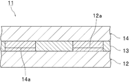
- FIG. 2 is a cross-sectional view schematically showing a modification of the connection structure shown in FIG.
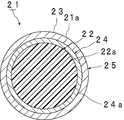
- FIG. 3 is a cross-sectional view schematically showing conductive particles that can be used in the curable composition for electronic components according to one embodiment of the present invention.
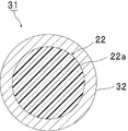
- FIG. 4 is a cross-sectional view showing a modification of the conductive particles.
- FIG. 5 is a cross-sectional view showing another modified example of conductive particles.
- the curable composition for electronic components according to the present invention includes a thermosetting compound, a latent curing agent, and an imidazole compound having an aromatic skeleton.
- the said curable composition is used for the connection of a copper electrode.
- the said curable composition is used for an electronic component.
- the said curable composition is used suitably for the connection of an electronic component. It is preferable that the said curable composition is a connection material for electronic components. It is preferable that the said curable composition is a circuit connection material for electronic components.
- the curable composition for electronic parts according to the present invention has the above-described composition, it can be quickly cured. Furthermore, since the curable composition for electronic components according to the present invention has the above-described composition, it is possible to improve conductivity when a copper electrode is connected.
- the surface of the copper electrode is usually heat-resistant preflux treated.
- electroconductivity can be improved.
- the imidazole compound having an aromatic skeleton greatly contributes to the improvement of the conductivity of the copper electrode.
- the thermosetting compound cannot be sufficiently cured, or the storage stability of the composition is low. It becomes low, or the curing rate of the composition becomes slow.
- thermosetting compound is rapidly cured mainly by the latent curing agent, and the conductivity of the copper electrode is enhanced mainly by the imidazole compound having the aromatic skeleton. Therefore, in the present invention, there is a great significance in combining the latent curing agent and the imidazole compound having an aromatic skeleton in the connection of the copper electrode.
- the moisture and heat resistance of the cured product can be improved.
- the thermal shock resistance of the cured product can be improved.
- thermosetting compound examples include oxetane compounds, epoxy compounds, episulfide compounds, (meth) acrylic compounds, phenolic compounds, amino compounds, unsaturated polyester compounds, polyurethane compounds, silicone compounds, and polyimide compounds.
- oxetane compounds examples include oxetane compounds, epoxy compounds, episulfide compounds, (meth) acrylic compounds, phenolic compounds, amino compounds, unsaturated polyester compounds, polyurethane compounds, silicone compounds, and polyimide compounds.
- the said thermosetting compound only 1 type may be used and 2 or more types may be used together.
- the epoxy compound has a property that the cured product has high adhesive strength and is excellent in water resistance and heat resistance of the cured product. Therefore, the thermosetting compound is preferably an epoxy compound.
- the above epoxy compounds include bisphenol type epoxy compounds, phenol novolac type epoxy compounds, biphenyl novolac type epoxy compounds, biphenol type epoxy compounds, resorcin type epoxy compounds, naphthalene type epoxy compounds, fluorene type epoxy compounds, phenol aralkyl type epoxy compounds, naphthol.
- Examples include aralkyl type epoxy compounds, dicyclopentadiene type epoxy compounds, anthracene type epoxy compounds, epoxy compounds having an adamantane skeleton, epoxy compounds having a tricyclodecane skeleton, and epoxy compounds having a triazine nucleus in the skeleton.
- the bisphenol type epoxy compound include a bisphenol A type epoxy compound, a bisphenol F type epoxy compound, and a bisphenol S type epoxy compound.
- the epoxy compound may have an epoxy group and a radical polymerizable group.
- the radical polymerizable group means a group capable of addition polymerization by a radical.
- examples of the radical polymerizable group include a group containing an unsaturated double bond.
- Specific examples of the radical polymerizable group include allyl group, isopropenyl group, maleoyl group, styryl group, vinylbenzyl group, (meth) acryloyl group and vinyl group.
- the (meth) acryloyl group means an acryloyl group and a methacryloyl group.
- the radical polymerizable group preferably has a vinyl group, and more preferably a (meth) acryloyl group.
- the radical polymerizable group is a (meth) acryloyl group
- the radical polymerizable group has a vinyl group.
- the epoxy compound preferably has an epoxy group at both ends.
- the epoxy compound preferably has a vinyl group in the side chain, preferably has a (meth) acryloyl group, and has a (meth) acryloyl group in the side chain. It is preferable.
- the weight average molecular weight of the epoxy compound is preferably 500 or more, more preferably 1000 or more, preferably 150,000 or less, more preferably 50000 or less. More preferably, it is 15000 or less.
- the weight average molecular weight of the epoxy compound indicates a weight average molecular weight in terms of polystyrene measured by gel permeation chromatography (GPC).
- the epoxy compound is a reaction product using a diol compound and a compound having two epoxy groups.
- the epoxy compound is preferably obtained by reacting a reaction product of a diol compound and a compound having two epoxy groups with a compound having a vinyl group or a compound having an epoxy group.
- the epoxy compound preferably has at least one vinyl group in the side chain, and more preferably has at least two vinyl groups in the side chain in total. As the number of vinyl groups increases, the heating time can be further shortened, and the adhesiveness and heat-and-moisture resistance of the cured product can be further improved.
- the epoxy compound is preferably a reaction product of a compound having two or more phenolic hydroxyl groups and a compound having two or more epoxy groups.
- Examples of the compound having two or more phenolic hydroxyl groups include bisphenol compounds, resorcinol and naphthalenol.
- Examples of the bisphenol compound include bisphenol F, bisphenol A, bisphenol S, bisphenol SA, and bisphenol E.
- Examples of the epoxy compound having two or more epoxy groups include aliphatic epoxy compounds and aromatic epoxy compounds.
- Examples of the aliphatic epoxy compound include a compound having a glycidyl ether group at both ends of an alkyl chain having 3 to 12 carbon atoms and a polyether skeleton having 2 to 4 carbon atoms. Examples thereof include polyether type epoxy compounds having structural units bonded continuously.
- the epoxy compound has a radical polymerizable group in a reaction product of bisphenol F or resorcinol and 1,6-hexanediol diglycidyl ether or resorcinol diglycidyl ether (hereinafter sometimes referred to as a reaction product X). It is preferably obtained by reacting a compound. In this reaction, the reaction is performed so that the radical polymerizable group remains. Epoxy compounds synthesized using such compounds can be cured more rapidly, and the adhesiveness and heat-and-moisture resistance of the cured product can be further enhanced.
- the compound having a radical polymerizable group is preferably (meth) acrylic acid or (meth) acryloyloxyethyl isocyanate.
- Examples of the reactant X include a first reaction product of bisphenol F and 1,6-hexanediol diglycidyl ether, a second reaction product of resorcinol and 1,6-hexanediol diglycidyl ether, resorcinol and resorcinol diester. And a third reactant with glycidyl ether and a fourth reactant with bisphenol F and resorcinol diglycidyl ether.
- the first reaction product has a structural unit in the main chain in which a skeleton derived from bisphenol F and a skeleton derived from 1,6-hexanediol diglycidyl ether are bonded, and 1,6-hexanediol diglycidyl. It has an epoxy group derived from ether at both ends.
- the second reaction product has a structural unit derived from resorcinol and a structural unit derived from 1,6-hexanediol diglycidyl ether in the main chain, and is derived from 1,6-hexanediol diglycidyl ether. It has an epoxy group at both ends.
- the third reaction product has a skeleton derived from resorcinol and a skeleton derived from resorcinol diglycidyl ether in the main chain, and has an epoxy group derived from resorcinol diglycidyl ether at both ends.
- the fourth reaction product has a skeleton derived from bisphenol F and a skeleton derived from resorcinol diglycidyl ether in the main chain, and an epoxy group derived from resorcinol diglycidyl ether at both ends.
- the first, second, third, and fourth Of the reactants, the first reactant, the second reactant, or the third reactant is preferred.
- the reactant X is preferably the first reactant, preferably the second reactant, and further preferably the third reactant.
- latent curing agent examples include a latent imidazole curing agent, a latent amine curing agent, a latent phenol curing agent, a boron trifluoride-amine complex, and an organic acid hydrazide.
- the latent curing agent may or may not have an aromatic skeleton.
- the said latent hardening agent only 1 type may be used and 2 or more types may be used together.
- Latent imidazole curing agent Commercially available products of the latent imidazole curing agent include clathrate imidazole compounds “TEP-2MZ”, “TEP-2E4MZ” and “TEP-1B2MZ” manufactured by Nippon Soda Co., Ltd., and “Cureduct P” manufactured by Shikoku Kasei Kogyo Co., Ltd. -0505 "and the like.
- latent amine curing agent examples include dicyandiamide, a modified amine compound, and an amine adduct compound.
- modified amine compounds examples include “Fujicure FXR-1020”, “Fujicure FXR-1030” and “Fujicure FXR-1081” manufactured by T & K TOKA.
- examples of the amine adduct compound include “Amure PN-23”, “Amure PN-H”, “Amure PN-31”, “Amure PN-40”, “Amure PN-50”, and “Amicure” manufactured by Ajinomoto Finetech.
- the latent curing agent is preferably a latent imidazole curing agent, and more preferably a microcapsule type imidazole curing agent.
- the latent curing agent is more preferably a microcapsule type latent curing agent, and more preferably a microcapsule type imidazole curing agent.
- the content of the latent curing agent with respect to 100 parts by weight of the thermosetting compound is preferably 1 part by weight or more, more preferably 5 parts by weight or more, preferably 65 parts by weight or less, more preferably 55 parts by weight or less. It is.
- the content of the latent curing agent is not less than the above lower limit and not more than the above upper limit, the quick curability of the composition and the conductivity between the copper electrodes are improved in a well-balanced manner.
- the imidazole compound having the aromatic skeleton is not a latent curing agent. As the imidazole compound having the aromatic skeleton, the latent curing agent is excluded. The latent curing agent contained in the curable composition is different from the imidazole compound having an aromatic skeleton contained in the curable composition. As for the imidazole compound which has the said aromatic skeleton, only 1 type may be used and 2 or more types may be used together.
- the aromatic skeleton examples include an aryl skeleton, a naphthalene skeleton, and an anthracene skeleton. From the viewpoint of effectively increasing the conductivity between the copper electrodes, the aromatic skeleton is preferably an aryl skeleton, and more preferably a phenyl skeleton.
- Examples of the imidazole compound having an aromatic skeleton include 2-phenylimidazole, 2-phenyl-4-methylimidazole, 1-benzyl-2-methylimidazole, 1-benzyl-2-phenylimidazole, 1-benzyl-2-methyl.
- the content of the imidazole compound having an aromatic skeleton with respect to 100 parts by weight of the thermosetting compound is preferably 0.1 parts by weight or more, more preferably 0.5 parts by weight or more, preferably 10 parts by weight or less. More preferably, it is 5 parts by weight or less.
- the content of the imidazole compound having an aromatic skeleton is not less than the above lower limit and not more than the above upper limit, the fast curability of the composition and the conductivity between the copper electrodes are improved in a well-balanced manner.
- the curable composition may further contain a flux, an adhesive strength adjusting agent, an inorganic filler, a solvent, a storage stabilizer, an ion scavenger, a silane coupling agent, or the like as necessary.
- the curable compound preferably contains a flux. Use of the flux further increases the conductivity of the copper electrode.
- a known flux can be used as the flux. As for the said flux, only 1 type may be used and 2 or more types may be used together.
- the above flux is not particularly limited.
- the flux it is possible to use a flux generally used for soldering or the like.
- the flux include zinc chloride, a mixture of zinc chloride and an inorganic halide, a mixture of zinc chloride and an inorganic acid, a molten salt, phosphoric acid, a derivative of phosphoric acid, an organic halide, hydrazine, an organic acid, and pine resin. Etc.
- Examples of the molten salt include ammonium chloride.
- Examples of the organic acid include lactic acid, citric acid, stearic acid, and glutamic acid.
- Examples of the pine resin include activated pine resin and non-activated pine resin.
- the flux is preferably rosin. By using rosin, the connection resistance between the electrodes is further reduced.
- the above rosins are rosins whose main component is abietic acid.
- the flux is preferably a rosin, and more preferably abietic acid. By using this preferable flux, the connection resistance between the electrodes is further reduced.
- the flux is preferably an organic acid having a carboxyl group.
- the compound having a carboxyl group include a compound having a carboxyl group bonded to an alkyl chain and a compound having a carboxyl group bonded to an aromatic ring. In these compounds having a carboxyl group, a hydroxyl group may be further bonded to an alkyl chain or an aromatic ring.
- the number of carboxyl groups bonded to the alkyl chain or aromatic ring is preferably 1 to 3, more preferably 1 or 2.
- the number of carbon atoms in the alkyl chain in the compound in which a carboxyl group is bonded to the alkyl chain is preferably 3 or more, preferably 8 or less, more preferably 6 or less.
- Specific examples of the compound having a carboxyl group bonded to an alkyl chain include hexanoic acid (5 carbon atoms, 1 carboxyl group), glutaric acid (4 carbon atoms, 2 carboxyl groups), and the like.
- Specific examples of the compound having a carboxyl group and a hydroxyl group include malic acid and citric acid.
- Specific examples of the compound having a carboxyl group bonded to an aromatic ring include benzoic acid, phthalic acid, benzoic anhydride, and phthalic anhydride.
- the content of the flux is preferably 0.5 parts by weight or more, more preferably 1 part by weight or more, preferably 10 parts by weight or less, more preferably 5 parts by weight or less with respect to 100 parts by weight of the thermosetting compound. is there.
- the content of the flux is not less than the above lower limit and not more than the upper limit, the effect of adding the flux is more effectively exhibited. For this reason, the flux effect in a composition becomes high, for example, the electroconductivity of a copper electrode becomes still higher.
- the curable composition for electronic parts containing conductive particles
- the curable composition can be used as a conductive material.
- the conductive material is preferably an anisotropic conductive material.
- the conductive particles electrically connect the electrodes of the connection target members.
- the conductive particles electrically connect, for example, electrodes between a circuit board and a semiconductor chip.
- the conductive particles are not particularly limited as long as they are conductive particles.
- the said electroconductive particle should just have an electroconductive part on the electroconductive surface.
- Examples of the conductive particles include organic particles, inorganic particles other than metal particles, organic-inorganic hybrid particles, or metal particles whose surfaces are covered with a conductive layer (metal layer), or substantially only metal. Examples thereof include metal particles.
- FIG. 3 is a sectional view showing conductive particles that can be used in the curable composition for electronic parts according to one embodiment of the present invention.
- the 3 has resin particles 22 (base material particles) and a conductive layer 23 disposed on the surface 22a of the resin particles 22.
- the conductive layer 23 covers the surface 22 a of the resin particle 22.
- the conductive particles 21 are coated particles in which the surface 22 a of the resin particle 22 is covered with the conductive layer 23. Accordingly, the conductive particles 21 have the conductive layer 23 on the surface 21a.
- metal particles or the like may be used.
- the conductive layer 23 includes a first conductive layer 24 disposed on the surface 22 a of the resin particle 22 and a solder layer 25 (solder, second conductive layer) disposed on the surface 24 a of the first conductive layer 24. ).
- the outer surface layer of the conductive layer 23 is a solder layer 25. Therefore, the conductive particles 21 have the solder layer 25 as a part of the conductive layer 23, and further, the first is separated from the resin layer 22 and the solder layer 25 as a part of the conductive layer 23.
- the conductive layer 24 is provided.
- the conductive layer 23 may have a multilayer structure, or may have a stacked structure of two or more layers.
- the conductive layer 23 has a two-layer structure.
- the conductive particles 31 may have a solder layer 32 as a single conductive layer.
- the at least outer surface layer (surface) of the conductive layer in the conductive particles may be a solder layer (solder).
- the conductive particles 21 are preferable among the conductive particles 21 and the conductive particles 31 because the conductive particles can be easily produced.
- the conductive particles 41 that are solder particles that do not have the core particles in the core and are not core-shell particles may be used.
- the conductive particles 41 are also formed of solder at the center.
- Conductive particles 21, 31, 41 can be used for the conductive material.
- the conductive part is not particularly limited. Gold, silver, copper, nickel, palladium, tin, etc. are mentioned as a metal which comprises the said electroconductive part.
- Examples of the conductive layer include a gold layer, a silver layer, a copper layer, a nickel layer, a palladium layer, or a conductive layer containing tin.
- the conductive particle is composed of a resin particle and a conductive layer (on the surface of the resin particle ( First conductive layer).
- the conductive particles are preferably conductive particles having at least a conductive outer surface of a low melting point metal layer.
- the conductive particles include base particles and a conductive layer disposed on the surface of the base particles, and at least the outer surface of the conductive layer. Is more preferably a low melting point metal layer. More preferably, the conductive particles include resin particles and a conductive layer disposed on the surface of the resin particles, and at least the outer surface of the conductive layer is a low melting point metal layer.
- the low melting point metal layer is a layer containing a low melting point metal.
- the low melting point metal is a metal having a melting point of 450 ° C. or lower.
- the melting point of the low melting point metal is preferably 300 ° C. or lower, more preferably 160 ° C. or lower.
- the low melting point metal preferably contains tin. In 100% by weight of the metal contained in the low melting point metal, the content of tin is preferably 30% by weight or more, more preferably 40% by weight or more, still more preferably 70% by weight or more, and particularly preferably 90% by weight or more. When the content of tin in the low melting point metal is not less than the lower limit, the connection reliability between the low melting point metal and the electrode is further enhanced.
- the tin content is determined using a high-frequency inductively coupled plasma emission spectrometer (“ICP-AES” manufactured by Horiba, Ltd.) or a fluorescent X-ray analyzer (“EDX-800HS” manufactured by Shimadzu). It can be measured.
- the conductive particles are preferably conductive particles whose outer surface of the conductive material is solder.
- the outer surface of the conductive part is a low melting point metal layer
- the low melting point metal layer is melted and joined to the electrodes, and the low melting point metal layer conducts between the electrodes.
- the connection resistance is lowered.
- the use of conductive particles having at least a conductive outer surface of the low melting point metal layer increases the bonding strength between the low melting point metal layer and the electrode. It becomes difficult to occur, and the conduction reliability is effectively increased.
- the low melting point metal constituting the low melting point metal layer is not particularly limited.
- the low melting point metal is preferably tin or an alloy containing tin.
- the alloy include a tin-silver alloy, a tin-copper alloy, a tin-silver-copper alloy, a tin-bismuth alloy, a tin-zinc alloy, and a tin-indium alloy.
- the low melting point metal is preferably tin, a tin-silver alloy, a tin-silver-copper alloy, a tin-bismuth alloy, or a tin-indium alloy because of its excellent wettability with respect to the electrode. More preferred are a tin-bismuth alloy and a tin-indium alloy.
- the low melting point metal is preferably solder.
- the material which comprises the said solder is not specifically limited, Based on JIS Z3001: welding terminology, it is preferable that it is a filler material whose liquidus is 450 degrees C or less.
- the solder composition include metal compositions containing zinc, gold, lead, copper, tin, bismuth, indium and the like. Of these, a tin-indium system (117 ° C. eutectic) or a tin-bismuth system (139 ° C. eutectic) which is low-melting and lead-free is preferable. That is, the solder preferably does not contain lead, and is preferably a solder containing tin and indium or a solder containing tin and bismuth.
- the low melting point metal is nickel, copper, antimony, aluminum, zinc, iron, gold, titanium, phosphorus, germanium, tellurium, cobalt, bismuth, manganese. Further, it may contain a metal such as chromium, molybdenum and palladium. From the viewpoint of further increasing the bonding strength between the low melting point metal and the electrode, the low melting point metal preferably contains nickel, copper, antimony, aluminum, or zinc.
- the content of these metals for increasing the bonding strength is 100 wt% of the low-melting point metal, preferably 0.0001 wt% or more, preferably 1% by weight or less.
- the conductive particles include resin particles and a conductive layer disposed on the surface of the resin particles, and the outer surface of the conductive layer is a low-melting metal layer, and the resin particles and the low-melting metal In addition to the low melting point metal layer, it is preferable to have a second conductive layer between the layers (such as solder layers). In this case, the low melting point metal layer is a part of the entire conductive layer, and the second conductive layer is a part of the entire conductive layer.
- the second conductive layer different from the low melting point metal layer preferably contains a metal.
- the metal constituting the second conductive layer is not particularly limited. Examples of the metal include gold, silver, copper, platinum, palladium, zinc, lead, aluminum, cobalt, indium, nickel, chromium, titanium, antimony, bismuth, germanium, cadmium, and alloys thereof. Further, tin-doped indium oxide (ITO) may be used as the metal. As for the said metal, only 1 type may be used and 2 or more types may be used together.
- the second conductive layer is preferably a nickel layer, a palladium layer, a copper layer or a gold layer, more preferably a nickel layer or a gold layer, and even more preferably a copper layer.
- the conductive particles preferably have a nickel layer, a palladium layer, a copper layer, or a gold layer, more preferably have a nickel layer or a gold layer, and still more preferably have a copper layer.
- a low melting point metal layer can be more easily formed on the surface of these preferable conductive layers.
- the second conductive layer may be a low melting point metal layer such as a solder layer.
- the conductive particles may have a plurality of low melting point metal layers.
- the thickness of the low melting point metal layer is preferably 0.1 ⁇ m or more, more preferably 0.5 ⁇ m or more, still more preferably 1 ⁇ m or more, preferably 50 ⁇ m or less, more preferably 10 ⁇ m or less, still more preferably 5 ⁇ m or less, particularly preferably. 3 ⁇ m or less.
- the conductivity is sufficiently high.
- the thickness of the low melting point metal layer is not more than the above upper limit, the difference in thermal expansion coefficient between the resin particles and the low melting point metal layer becomes small, and the low melting point metal layer is hardly peeled off.
- the total thickness of the conductive layer is preferably 0.1 ⁇ m or more, more preferably 0.5 ⁇ m or more, Preferably it is 1 micrometer or more, Preferably it is 50 micrometers or less, More preferably, it is 10 micrometers or less, More preferably, it is 5 micrometers or less, Most preferably, it is 3 micrometers or less.
- the average particle size of the conductive particles is preferably 100 ⁇ m or less, more preferably 20 ⁇ m or less, still more preferably less than 20 ⁇ m, still more preferably 15 ⁇ m or less, and particularly preferably 10 ⁇ m or less.
- the average particle diameter of the conductive particles is preferably 0.5 ⁇ m or more, more preferably 1 ⁇ m or more. From the viewpoint of further improving the connection reliability of the connection structure when subjected to a thermal history, the average particle diameter of the conductive particles is particularly preferably 1 ⁇ m or more and 10 ⁇ m or less, and is 1 ⁇ m or more and 4 ⁇ m or less. Most preferred.
- the average particle size of the conductive particles is also preferably 3 ⁇ m or less.
- the average particle size of the conductive particles is particularly preferably 1 ⁇ m or more and 100 ⁇ m or less. .
- the “average particle size” of the conductive particles indicates a number average particle size.
- the average particle diameter of the conductive particles can be obtained by observing 50 arbitrary conductive particles with an electron microscope or an optical microscope and calculating an average value.
- the surface of the conductive particles may be insulated with an insulating material such as insulating particles, flux, or the like. It is preferable that the insulating material, the flux, and the like are removed from the connection portion by being softened and flowed by heat at the time of connection. Thereby, the short circuit between electrodes is suppressed.
- an insulating material such as insulating particles, flux, or the like. It is preferable that the insulating material, the flux, and the like are removed from the connection portion by being softened and flowed by heat at the time of connection. Thereby, the short circuit between electrodes is suppressed.
- the content of the conductive particles is not particularly limited. In 100% by weight of the curable composition, the content of the conductive particles is preferably 0.1% by weight or more, more preferably 0.5% by weight or more, preferably 40% by weight or less, more preferably 20% by weight. Hereinafter, it is more preferably 15% by weight or less.
- a conductive particle can be easily arrange
- the said curable composition can be used in order to adhere
- the said curable composition is used for the connection of a copper electrode.
- the curable composition may be a film or a paste.
- the curable composition is preferably a paste.
- the initial connection resistance is further reduced.
- the connection resistance after being exposed to impact or high temperature and high humidity can be effectively kept low.
- the conductive material can be used as a conductive paste, a conductive film, or the like.
- the conductive material is used as a conductive film, a film not containing conductive particles may be laminated on the conductive film containing conductive particles.
- the film includes a sheet.
- the curable composition is preferably a paste-like conductive paste.
- the conductive paste is preferably an anisotropic conductive paste.
- the conductive film is preferably an anisotropic conductive film.
- the curable composition includes an electrode first connection target member having a first electrode on the surface, a second connection target member having a second electrode on the surface, the first connection target member, and the first connection target member. It is used suitably in order to obtain a connection structure provided with the connection part which has connected 2 connection object members.
- the connection part is formed by curing the curable composition.
- at least one of the first electrode and the second electrode is a copper electrode.
- the first electrode and the second electrode are electrically connected. More preferably, both the first electrode and the second electrode are copper electrodes.
- connection structure in which the curable composition for electronic parts includes conductive particles, and the first electrode and the second electrode are electrically connected by the conductive particles.
- the electronic component is provided between the first connection target member having the first electrode on the surface and the second connection target member having the second electrode on the surface.
- a connecting portion connecting the first connection target member and the second connection target member is formed by curing the curable composition for electronic components, and a step of arranging the curable composition for the electronic component And a step of obtaining a connection structure in which the first electrode and the second electrode are electrically connected.
- At least one of the first electrode and the second electrode is a copper electrode.
- the curable composition for electronic parts includes conductive particles, and the first electrode and the second electrode are electrically connected by the conductive particles. It is preferable to obtain a connecting structure.
- FIG. 1 schematically shows a cross-sectional view of an example of a connection structure using a curable composition according to an embodiment of the present invention.
- connection structure 1 shown in FIG. 1 is a connection that connects the first connection target member 2, the second connection target member 4, and the first connection target member 2 and the second connection target member 4.
- Part 3 is a cured product layer and is formed by curing a curable composition for electronic parts (conductive material) including the conductive particles 5.
- the first connection object member 2 has a plurality of first electrodes 2a on the surface (upper surface).
- the second connection target member 4 has a plurality of second electrodes 4a on the surface (lower surface). At least one of the first electrode 2a and the second electrode 4a is a copper electrode.
- the first electrode 2 a and the second electrode 4 a are electrically connected by one or a plurality of conductive particles 5. Therefore, the first and second connection target members 2 and 4 are electrically connected by the conductive particles 5.
- connection between the first and second electrodes 2a and 4a is usually performed by connecting the first connection target member 2 and the second connection target member 4 with the first and second electrodes 2a through the curable composition. , 4a are overlapped so as to face each other, and then the curable composition is cured by pressurization. Generally, the conductive particles 5 are compressed by pressurization.
- the first and second connection target members are not particularly limited.
- the first and second connection target members include electronic components such as semiconductor chips, capacitors, and diodes, and circuit boards such as printed boards, flexible printed boards, glass epoxy boards, and glass boards. Examples include parts.
- the said curable composition does not need to contain electroconductive particle.
- the electrodes of the first and second connection target members can be electrically connected, for example, by bringing the electrodes into contact with each other without electrically connecting the electrodes with the conductive particles.
- FIG. 2 is a cross-sectional view schematically showing a modification of the connection structure shown in FIG.
- connection structure 11 shown in FIG. 2 is a connection that connects the first connection target member 12, the second connection target member 14, and the first connection target member 12 and the second connection target member 14.
- Unit 13 The connection part 13 is a hardened
- the first connection object member 12 has a plurality of first electrodes 12a on the surface (upper surface).
- the second connection target member 14 has a plurality of second electrodes 14a on the surface (lower surface). At least one of the first electrode 12a and the second electrode 14a is a copper electrode.
- the first electrode 12a and the second electrode 14a are, for example, bump electrodes.
- the first electrode 12a and the second electrode 14a are electrically connected to each other without being in contact with conductive particles. Therefore, the 1st, 2nd connection object members 12 and 14 are electrically connected.
- the conductive material is, for example, a connection between a flexible printed circuit board and a glass substrate (FOG (Film on Glass)), a connection between a semiconductor chip and a flexible printed circuit board (COF ( (Chip on Film)), connection between a semiconductor chip and a glass substrate (COG (Chip on Glass)), connection between a flexible printed circuit board and a glass epoxy substrate (FOB (Film on Board)), or the like.
- the said electrically-conductive material is suitable for a FOG use or a COG use, and is more suitable for a COG use.
- the curable composition is preferably a conductive material used for connection between the flexible printed circuit board and the glass substrate, or between the semiconductor chip and the flexible printed circuit board, and is used for connection between the semiconductor chip and the flexible printed circuit board. More preferably, it is a conductive material.
- Thermosetting compound Thermosetting compound 1 (epoxy group-containing polymer, “MARPROOF G-01100” manufactured by NOF Corporation, weight average molecular weight: 12000, Tg: 47 ° C., epoxy equivalent: 170 g / eq)
- Thermosetting compound 2 resorcinol type epoxy compound, “EX-201” manufactured by Nagase ChemteX Corporation
- Thermosetting compound 3 Triazine triglycidyl ether, “TEPIC-SS” manufactured by Nissan Chemical Co., Ltd.
- Latent curing agent Latent curing agent
- Latent curing agent 1 inclusion imidazole compound, “TEP-2MZ” manufactured by Nippon Soda Co., Ltd.
- Latent curing agent 2 epoxy-imidazole adduct, “Cure Duct P-0505” manufactured by Shikoku Kasei Kogyo Co., Ltd.
- Latent curing agent 3 ((Microcapsule type latent curing agent), “Novacure HX3921HP” manufactured by Asahi Kasei E-Materials)
- Latent curing agent 4 ((Microcapsule type latent curing agent), “Novacure HX3941HP” manufactured by Asahi Kasei E-Materials)
- Aromatic skeleton-containing imidazole compound 1 (“2-phenylimidazole” manufactured by Shikoku Chemicals)
- Aromatic skeleton-containing imidazole compound 2 (“2-phenyl-4-methylimidazole” manufactured by Shikoku Chemicals)
- Aromatic skeleton-containing imidazole compound 3 (“Benzimidazole” manufactured by Wako Pure Chemical Industries, Ltd.)
- Aromatic skeleton-containing imidazole compound 4 (“2-methylbenzimidazole” manufactured by Wako Pure Chemical Industries, Ltd.)
- Conductive particles 1 SnBi solder particles ("Sn58Bi-20” manufactured by Fukuda Metals Co., Ltd., average particle size 4.5 ⁇ m)
- Conductive particles 2 (resin core solder coated particles, prepared by the following procedure)
- Divinylbenzene resin particles (“Micropearl SP-207” manufactured by Sekisui Chemical Co., Ltd., average particle diameter 7 ⁇ m, softening point 330 ° C., 10% K value (23 ° C.) 4 GPa) are electroless nickel plated on the surface of the resin particles A base nickel plating layer having a thickness of 0.1 ⁇ m was formed.
- Conductive particles (average particle size 14 ⁇ m, CV value 22%, resin core solder-coated particles) were prepared.
- Conductive particles 3 Au plated particles of divinylbenzene resin particles (“Au-210” manufactured by Sekisui Chemical Co., Ltd., average particle size 10 ⁇ m)
- Filler Nanosilica, “MT-10” manufactured by Tokuyama
- Adhesive agent KBE-403” manufactured by Shin-Etsu Chemical Co., Ltd.
- Flux Glutaric acid” manufactured by Wako Pure Chemical Industries, Ltd.
- Phenoxy resin YP-50S manufactured by Nippon Steel & Sumikin Chemical Co., Ltd.
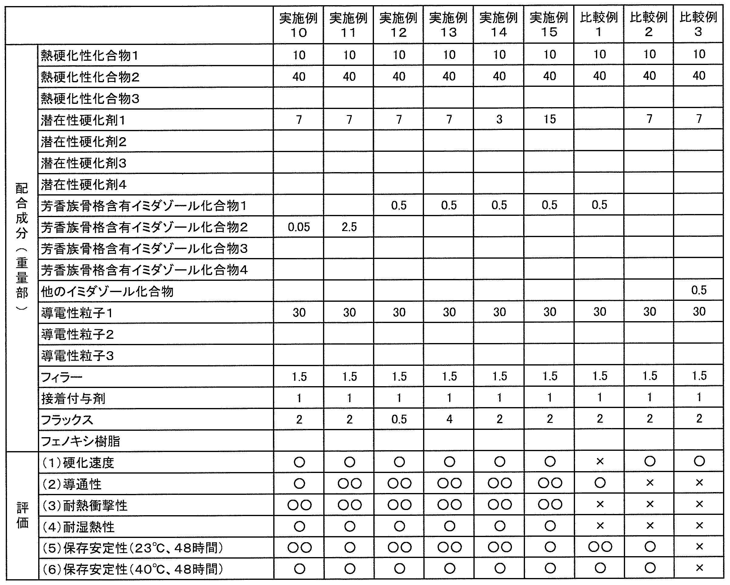
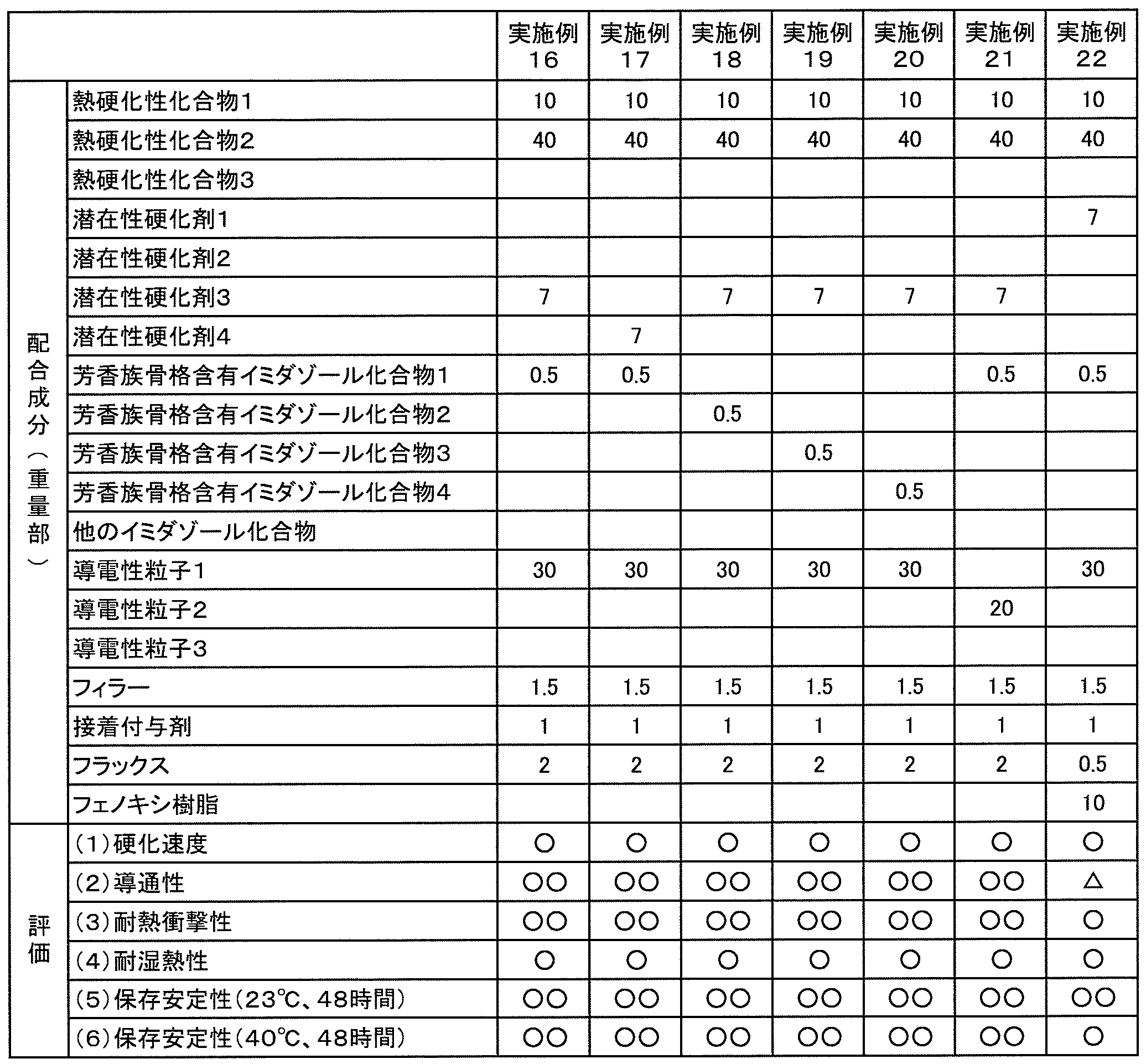
- Examples 1 to 21 and Comparative Examples 1 to 3 The components shown in the following Tables 1 to 3 were blended in the blending amounts shown in the following Tables 1 to 3, and stirred at 2000 rpm for 5 minutes using a planetary stirrer to obtain an anisotropic conductive paste.
- Example 22 10 parts by weight of phenoxy resin (“YP-50S” manufactured by Nippon Steel & Sumikin Chemical Co., Ltd.) was dissolved in methyl ethyl ketone (MEK) so that the solid content was 50% by weight to obtain a solution.
- Ingredients other than the phenoxy resin shown in Table 3 below were blended with the amounts shown in Table 3 below and the total amount of the above solution, and after stirring for 5 minutes at 2000 rpm using a planetary stirrer, a bar coater was used. It was used and coated on a release PET (polyethylene terephthalate) film so that the thickness after drying was 30 ⁇ m.
- An anisotropic conductive film was obtained by removing MEK by vacuum drying at room temperature.
- connection structure used in evaluation items (1) to (3): A glass epoxy substrate (FR-4 substrate) having 70 copper electrodes on the upper surface with an electrode pattern having an L / S of 100 ⁇ m / 100 ⁇ m was prepared. Moreover, the flexible printed circuit board which has 70 copper electrodes on the lower surface with the electrode pattern whose L / S is 100 micrometers / 100 micrometers was prepared. The FR-4 substrate and the flexible printed circuit board were designed so that a daisy chain could be formed by overlapping them.
- the obtained anisotropic conductive paste was applied on the upper surface of the glass epoxy substrate so as to have a thickness of 200 ⁇ m to form an anisotropic conductive paste layer.
- the flexible printed circuit board was laminated on the anisotropic conductive paste layer so that the electrodes face each other. Then, while adjusting the temperature of the thermocompression bonding head so that the temperature of the anisotropic conductive paste layer becomes 170 ° C. (final pressure bonding temperature), the pressure bonding head is placed on the upper surface of the flexible printed circuit board and a pressure of 1 MPa is applied. Then, the anisotropic conductive paste layer was cured until curing was completed at 170 ° C. to obtain a connection structure (FOB).
- FAB connection structure
- connection resistances 20 connection resistances were evaluated by a four-terminal method.
- the conductivity was determined according to the following criteria.
- ⁇ Average value of connection resistance is 8.0 ⁇ or less ⁇ : Average value of connection resistance exceeds 8.0 ⁇ and 10.0 ⁇ or less ⁇ : Average value of connection resistance exceeds 10.0 ⁇ and 15.0 ⁇ or less ⁇ Average connection resistance exceeds 15.0 ⁇
- Thermal shock resistance was determined according to the following criteria.
- connection resistance In all 10 connection structures, the rate of increase in connection resistance from the connection resistance before the thermal cycle test is 5% or less.
- ⁇ Connection resistance before the thermal cycle test in all 10 connection structures. The connection resistance rise rate from 5 to exceeds 10% and 10% or less ⁇ : Of 10 connection structures, the connection structure from which the connection resistance increase rate before the thermal cycle test exceeds 10% Have more than one body
- the moisture and heat resistance was evaluated by a bias test. Specifically, a glass epoxy substrate (FR-4 substrate) having 70 comb-shaped copper electrode patterns with L / S of 100 ⁇ m / 100 ⁇ m on the upper surface was prepared. Moreover, the flexible printed circuit board which has 70 comb-shaped copper electrode patterns with L / S of 100 micrometers / 100 micrometers on the lower surface was prepared. A connection structure was obtained by the same method as that for producing the connection structure used for the evaluation items (1) to (3). The patterns of the FR-4 substrate and the flexible printed circuit board were designed so that a comb pattern could be formed by overlapping. Wet heat resistance was determined according to the following criteria.
- Resistance value is 10 8 ⁇ or more ⁇ : Resistance value is 5 ⁇ 10 7 ⁇ or more, less than 10 8 ⁇ ⁇ : Resistance value is 10 7 ⁇ or more, less than 5 ⁇ 10 7 ⁇ ⁇ : Resistance value is 10 7 ⁇ Less than
- Viscosity after standing for 48 hours / initial viscosity is less than 1.2
- Viscosity after standing for 48 hours / initial viscosity is 1.2 or more and less than 1.5
- Viscosity after standing for 48 hours / initial Viscosity is 1.5 or more
- Viscosity after standing for 48 hours / initial viscosity is less than 1.2
- Viscosity after standing for 48 hours / initial viscosity is 1.2 or more and less than 1.35
- connection structure using the glass epoxy board (connection object member) which has a copper electrode on the upper surface, and the flexible printed circuit board (connection object member) which has a copper electrode on the lower surface was shown. Even when only one of these two connection target members is a copper electrode and the remaining is an aluminum electrode, the evaluation results having the same tendency as the evaluation results shown in Tables 1 to 3 can be obtained. confirmed. In addition, when both the electrodes of these two connection object members were aluminum electrodes, the difference in the evaluation result of an Example and a comparative example was small.
Landscapes
- Engineering & Computer Science (AREA)
- Manufacturing & Machinery (AREA)
- Microelectronics & Electronic Packaging (AREA)
- Conductive Materials (AREA)
- Wire Bonding (AREA)
- Epoxy Resins (AREA)
- Compositions Of Macromolecular Compounds (AREA)
- Chemical & Material Sciences (AREA)
- Health & Medical Sciences (AREA)
- Chemical Kinetics & Catalysis (AREA)
- Medicinal Chemistry (AREA)
- Polymers & Plastics (AREA)
- Organic Chemistry (AREA)
Abstract
Description
本発明に係る電子部品用硬化性組成物(以下、硬化性組成物と略記することがある)は、熱硬化性化合物と、潜在性硬化剤と、芳香族骨格を有するイミダゾール化合物とを含む。上記硬化性組成物は、銅電極の接続に用いられる。上記硬化性組成物は電子部品に用いられる。上記硬化性組成物は、電子部品の接続に好適に用いられる。上記硬化性組成物は、電子部品用接続材料であることが好ましい。上記硬化性組成物は、電子部品用回路接続材料であることが好ましい。
上記熱硬化性化合物としては、オキセタン化合物、エポキシ化合物、エピスルフィド化合物、(メタ)アクリル化合物、フェノール化合物、アミノ化合物、不飽和ポリエステル化合物、ポリウレタン化合物、シリコーン化合物及びポリイミド化合物等が挙げられる。上記熱硬化性化合物は、1種のみが用いられてもよく、2種以上が併用されてもよい。
上記潜在性硬化剤としては、潜在性イミダゾール硬化剤、潜在性アミン硬化剤、潜在性フェノール硬化剤、三フッ化ホウ素-アミン錯体及び有機酸ヒドラジド等が挙げられる。上記潜在性硬化剤は、芳香族骨格を有していてもよく、有していなくてもよい。上記潜在性硬化剤は、1種のみが用いられてもよく、2種以上が併用されてもよい。
上記芳香族骨格を有するイミダゾール化合物は、潜在性硬化剤ではない。上記芳香族骨格を有するイミダゾール化合物として、潜在性硬化剤は除かれる。上記硬化性組成物に含まれる潜在性硬化剤と、上記硬化性組成物に含まれる芳香族骨格を有するイミダゾール化合物とは異なる。上記芳香族骨格を有するイミダゾール化合物は、1種のみが用いられてもよく、2種以上が併用されてもよい。
上記硬化性組成物は、必要に応じて、フラックス、接着力調整剤、無機充填剤、溶剤、貯蔵安定剤、イオン捕捉剤又はシランカップリング剤等をさらに含んでいてもよい。
上記硬化性組成物が導電性粒子を含む場合には、上記硬化性組成物を導電材料として用いることができる。上記導電材料は、異方性導電材料であることが好ましい。
上記硬化性組成物は、様々な接続対象部材を接着するために使用できる。但し、上記硬化性組成物は、銅電極の接続に用いられる。上記硬化性組成物は、フィルムであってもよく、ペーストであってもよい。上記硬化性組成物は、ペーストであることが好ましい。上記硬化性組成物がペーストであると、初期の接続抵抗がより一層低くなる。さらに、衝撃や高温高湿に晒された後の接続抵抗も効果的に低く維持できる。
熱硬化性化合物1(エポキシ基含有ポリマー、日油社製「MARPROOF G-01100」、重量平均分子量:12000、Tg:47℃、エポキシ当量:170g/eq)
熱硬化性化合物2(レゾルシノール型エポキシ化合物、ナガセケムテックス社製「EX-201」)
熱硬化性化合物3(トリアジントリグリシジルエーテル、日産化学社製「TEPIC-SS」)
潜在性硬化剤1(包接イミダゾール化合物、日本曹達社製「TEP-2MZ」)
潜在性硬化剤2(エポキシ-イミダゾールアダクト、四国化成工業社製「キュアダクト P-0505」)
潜在性硬化剤3((マイクロカプセル型潜在性硬化剤)、旭化成イーマテリアルズ社製社製「ノバキュアHX3921HP」)
潜在性硬化剤4((マイクロカプセル型潜在性硬化剤)、旭化成イーマテリアルズ社製社製「ノバキュアHX3941HP」)
芳香族骨格含有イミダゾール化合物1(四国化成工業社製「2-フェニルイミダゾール」)
芳香族骨格含有イミダゾール化合物2(四国化成工業社製「2-フェニル-4-メチルイミダゾール」)
芳香族骨格含有イミダゾール化合物3(和光純薬工業社製「ベンゾイミダゾール」)
芳香族骨格含有イミダゾール化合物4(和光純薬工業社製「2-メチルベンゾイミダゾール」)
他のイミダゾール化合物(潜在性硬化剤ではない、芳香族骨格を有さない、四国化成工業社製「2-メチルイミダゾール」)
導電性粒子1:SnBiはんだ粒子(福田金属社製「Sn58Bi-20」、平均粒子径4.5μm)
導電性粒子2:(樹脂コアはんだ被覆粒子、下記手順で作製)
ジビニルベンゼン樹脂粒子(積水化学工業社製「ミクロパールSP-207」、平均粒子径7μm、軟化点330℃、10%K値(23℃)4GPa)を無電解ニッケルめっきし、樹脂粒子の表面上に厚さ0.1μmの下地ニッケルめっき層を形成した。次いで、下地ニッケルめっき層が形成された樹脂粒子を電解銅めっきし、厚さ1μmの銅層を形成した。更に、錫及びビスマスを含有する電解めっき液を用いて、電解めっきし、厚さ1μmのはんだ層を形成した。このようにして、樹脂粒子の表面上に厚み1μmの銅層が形成されており、該銅層の表面に厚み1μmのはんだ層(錫:ビスマス=43重量%:57重量%)が形成されている導電性粒子(平均粒子径14μm、CV値22%、樹脂コアはんだ被覆粒子)を作製した。
導電性粒子3:ジビニルベンゼン樹脂粒子のAuメッキ粒子(積水化学工業社製「Au-210」、平均粒子径10μm)
フィラー(ナノシリカ、トクヤマ社製「MT-10」)
接着付与剤(信越化学工業社製「KBE-403」)
フラックス(和光純薬工業社製「グルタル酸」)
フェノキシ樹脂(新日鉄住金化学社製「YP-50S」)
下記の表1~3に示す成分を下記の表1~3に示す配合量で配合して、遊星式攪拌機を用いて2000rpmで5分間攪拌することにより、異方性導電ペーストを得た。
フェノキシ樹脂(新日鉄住金化学社製「YP-50S」)10重量部をメチルエチルケトン(MEK)に固形分が50重量%となるように溶解させて、溶解液を得た。下記の表3に示すフェノキシ樹脂を除く成分を下記の表3に示す配合量と、上記溶解液の全量とを配合して、遊星式攪拌機を用いて2000rpmで5分間攪拌した後、バーコーターを用いて乾燥後の厚みが30μmになるよう離型PET(ポリエチレンテレフタレート)フィルム上に塗工した。室温で真空乾燥することで、MEKを除去することにより、異方性導電フィルムを得た。
(1)~(3)の評価項目で用いる接続構造体(FOB)の作製:
L/Sが100μm/100μmの電極パターンにて、70本の銅電極を上面に有するガラスエポキシ基板(FR-4基板)を用意した。また、L/Sが100μm/100μmの電極パターンにて、70本の銅電極を下面に有するフレキシブルプリント基板を用意した。FR-4基板と、フレキシブルプリント基板のパターンは、重ねあわせることによりデイジーチェーンが形成できるように設計した。
上記接続構造体を得る際に、加熱により異方性導電ペースト層が硬化するまでの時間を測定した。具体的には、上記接続構造体を得る手順で異方性導電ペーストを上記ガラスエポキシ基板に塗布した後に、170℃ホットプレート上にて、異方性導電ペースト層の表面のタック(安田精機製作所製のボールタックテスターにて、助走路:100mm、測定部:100mm、傾斜角度30°、ボールφ1/16が測定部にて停止しない程度の粘着性)がなくなるまでのゲル化時間を評価した。硬化速度を下記の基準で判定した。
○:表面のタックがなくなるまでのゲル化時間が3秒未満
×:表面のタックがなくなるまでのゲル化時間が3秒以上
得られた接続構造体を用いて、20箇所の接続抵抗を4端子法にて評価した。導通性を下記の基準で判定した。
○○:接続抵抗の平均値が8.0Ω以下
○:接続抵抗の平均値が8.0Ωを超え、10.0Ω以下
△:接続抵抗の平均値が10.0Ωを超え、15.0Ω以下
×接続抵抗の平均値が15.0Ωを超える
得られた接続構造体をそれぞれ10個用意し、-30℃で5分間保持し、次に80℃まで昇温させて5分間保持した後、-30℃まで降温する過程を1サイクルとし、1サイクル当たり1時間とする冷熱サイクル試験を実施した。500サイクル後に、それぞれ10個の接続構造体を取り出した。
○○:10個の接続構造体全てにおいて、冷熱サイクル試験前の接続抵抗からの接続抵抗の上昇率が5%以下である
○:10個の接続構造体全てにおいて、冷熱サイクル試験前の接続抵抗からの接続抵抗の上昇率が5%を超え、10%以下である
×:10個の接続構造体のうち、冷熱サイクル試験前の接続抵抗からの接続抵抗の上昇率が10%を超える接続構造体が1個以上ある
バイアス試験により、耐湿熱性を評価した。具体的には、L/Sが100μm/100μmの70本の櫛形銅電極パターンを上面に有するガラスエポキシ基板(FR-4基板)を用意した。また、L/Sが100μm/100μmの70本の櫛形銅電極パターンを下面に有するフレキシブルプリント基板を用意した。(1)~(3)の評価項目に用いた接続構造体の作製方法と同じ方法で、接続構造体を得た。FR-4基板と、フレキシブルプリント基板のパターンは、重ねあわせることにより櫛形パターンが形成できるように設計した。耐湿熱性を下記の基準で判定した。
○○:抵抗値が108Ω以上
○:抵抗値が5×10⁷Ω以上、108Ω未満
△:抵抗値が107Ω以上、5×10⁷Ω未満
×:抵抗値が107Ω未満
異方性導電ペーストを23℃にて48時間静置し、静置前後での粘度変化を、E型粘度計 TV-33(東機産業社製)を用いて測定した。静置前後での粘度変化から、保存安定性を下記の基準で判定した。
○○:48時間静置後の粘度/初期粘度が1.2未満
○:48時間静置後の粘度/初期粘度が1.2以上1.5未満
×:48時間静置後の粘度/初期粘度が1.5以上
異方性導電ペーストを40℃にて48時間静置し、静置前後での粘度変化を、E型粘度計 TV-33(東機産業社製)を用いて測定した。静置前後での粘度変化から、保存安定性を下記の基準で判定した。
○○:48時間静置後の粘度/初期粘度が1.2未満
○:48時間静置後の粘度/初期粘度が1.2以上1.35未満
△:48時間静置後の粘度/初期粘度が1.35以上1.5未満
×:48時間静置後の粘度/初期粘度が1.5以上

2,12…第1の接続対象部材
2a,12a…第1の電極
3,13…接続部
4,14…第2の接続対象部材
4a,14a…第2の電極
5…導電性粒子
21…導電性粒子
21a…表面
22…樹脂粒子
22a…表面
23…導電層
24…第1の導電層
24a…表面
25…はんだ層
25a…溶融したはんだ層部分
31…導電性粒子
32…はんだ層
41…はんだ粒子
Claims (9)
- 銅電極の接続に用いられる電子部品用硬化性組成物であって、
熱硬化性化合物と、潜在性硬化剤と、芳香族骨格を有するイミダゾール化合物とを含む、電子部品用硬化性組成物。 - 前記潜在性硬化剤が、マイクロカプセル型イミダゾール硬化剤である、請求項1に記載の電子部品用硬化性組成物。
- 導電性粒子を含む、請求項1又は2に記載の電子部品用硬化性組成物。
- 前記導電性粒子が、導電性の外側の表面がはんだである導電性粒子である、請求項3に記載の電子部品用硬化性組成物。
- ペーストである、請求項1~4のいずれか1項に記載の電子部品用硬化性組成物。
- 第1の電極を表面に有する第1の接続対象部材と、
第2の電極を表面に有する第2の接続対象部材と、
前記第1の接続対象部材と前記第2の接続対象部材とを接続している接続部とを備え、
前記接続部が、請求項1~5のいずれか1項に記載の電子部品用硬化性組成物を硬化させることにより形成されており、
前記第1の電極及び前記第2の電極の内の少なくとも一方が銅電極であり、
前記第1の電極と前記第2の電極とが電気的に接続されている、接続構造体。 - 前記電子部品用硬化性組成物が導電性粒子を含み、
前記第1の電極と前記第2の電極とが前記導電性粒子により電気的に接続されている、請求項6に記載の接続構造体。 - 第1の電極を表面に有する第1の接続対象部材と、第2の電極を表面に有する第2の接続対象部材との間に、請求項1~5のいずれか1項に記載の電子部品用硬化性組成物を配置する工程と、
前記電子部品用硬化性組成物を硬化させることにより、前記第1の接続対象部材と前記第2の接続対象部材とを接続している接続部を形成し、前記第1の電極と前記第2の電極とが電気的に接続されている接続構造体を得る工程とを備え、
前記第1の電極及び前記第2の電極の内の少なくとも一方が銅電極である、接続構造体の製造方法。 - 前記電子部品用硬化性組成物が導電性粒子を含み、
前記第1の電極と前記第2の電極とが前記導電性粒子により電気的に接続されている接続構造体を得る、請求項8に記載の接続構造体の製造方法。
Priority Applications (3)
| Application Number | Priority Date | Filing Date | Title |
|---|---|---|---|
| KR1020157002632A KR20150109322A (ko) | 2013-01-17 | 2014-01-16 | 전자 부품용 경화성 조성물, 접속 구조체 및 접속 구조체의 제조 방법 |
| JP2014504102A JP5681327B2 (ja) | 2013-01-17 | 2014-01-16 | 電子部品用硬化性異方性導電材料、接続構造体及び接続構造体の製造方法 |
| CN201480002105.9A CN104540869B (zh) | 2013-01-17 | 2014-01-16 | 电子部件用固化性组合物、连接结构体及连接结构体的制造方法 |
Applications Claiming Priority (2)
| Application Number | Priority Date | Filing Date | Title |
|---|---|---|---|
| JP2013-006583 | 2013-01-17 | ||
| JP2013006583 | 2013-01-17 |
Publications (1)
| Publication Number | Publication Date |
|---|---|
| WO2014112541A1 true WO2014112541A1 (ja) | 2014-07-24 |
Family
ID=51209630
Family Applications (1)
| Application Number | Title | Priority Date | Filing Date |
|---|---|---|---|
| PCT/JP2014/050616 Ceased WO2014112541A1 (ja) | 2013-01-17 | 2014-01-16 | 電子部品用硬化性組成物、接続構造体及び接続構造体の製造方法 |
Country Status (5)
| Country | Link |
|---|---|
| JP (1) | JP5681327B2 (ja) |
| KR (1) | KR20150109322A (ja) |
| CN (1) | CN104540869B (ja) |
| TW (1) | TWI582125B (ja) |
| WO (1) | WO2014112541A1 (ja) |
Cited By (7)
| Publication number | Priority date | Publication date | Assignee | Title |
|---|---|---|---|---|
| WO2016133113A1 (ja) * | 2015-02-19 | 2016-08-25 | 積水化学工業株式会社 | 導電ペースト及び接続構造体 |
| WO2016190244A1 (ja) * | 2015-05-25 | 2016-12-01 | 積水化学工業株式会社 | 導電材料及び接続構造体 |
| WO2017029993A1 (ja) * | 2015-08-19 | 2017-02-23 | 積水化学工業株式会社 | 導電材料及び接続構造体 |
| WO2017033930A1 (ja) * | 2015-08-24 | 2017-03-02 | 積水化学工業株式会社 | 導電材料及び接続構造体 |
| JP2018131569A (ja) * | 2017-02-16 | 2018-08-23 | パナソニックIpマネジメント株式会社 | 導電性粒子を含む樹脂組成物 |
| US20210375804A1 (en) * | 2020-06-01 | 2021-12-02 | Samsung Display Co., Ltd. | Display device and method of manufacturing the same |
| WO2023166973A1 (ja) * | 2022-03-02 | 2023-09-07 | ナミックス株式会社 | 硬化性樹脂組成物、接着剤、硬化物、カメラモジュール、及び電子機器 |
Families Citing this family (3)
| Publication number | Priority date | Publication date | Assignee | Title |
|---|---|---|---|---|
| JP6551794B2 (ja) * | 2016-05-30 | 2019-07-31 | パナソニックIpマネジメント株式会社 | 導電粒子、ならびに回路部材の接続材料、接続構造、および接続方法 |
| KR20180024099A (ko) * | 2016-08-26 | 2018-03-08 | 삼성디스플레이 주식회사 | 접합 조립체 및 이를 포함하는 표시 장치 |
| EP3979298A1 (en) * | 2020-09-30 | 2022-04-06 | Infineon Technologies Austria AG | Device for controlling trapped ions and method of manufacturing the same |
Citations (5)
| Publication number | Priority date | Publication date | Assignee | Title |
|---|---|---|---|---|
| JP2001081155A (ja) * | 1999-09-13 | 2001-03-27 | Sumitomo Bakelite Co Ltd | 半導体用樹脂ペースト及びそれを用いた半導体装置 |
| JP2012021114A (ja) * | 2010-07-16 | 2012-02-02 | Sekisui Chem Co Ltd | 硬化性組成物及び接続構造体 |
| JP2012092321A (ja) * | 2010-09-28 | 2012-05-17 | Sekisui Chem Co Ltd | 異方性導電材料、bステージ状硬化物及び接続構造体 |
| JP2012124479A (ja) * | 2011-11-24 | 2012-06-28 | Hitachi Chem Co Ltd | 半導体パッケージ |
| JP2012158730A (ja) * | 2011-02-03 | 2012-08-23 | Namics Corp | エポキシ樹脂組成物およびそれを用いた半導体封止材 |
Family Cites Families (1)
| Publication number | Priority date | Publication date | Assignee | Title |
|---|---|---|---|---|
| WO2000060614A1 (en) * | 1999-04-01 | 2000-10-12 | Mitsui Chemicals, Inc. | Anisotropically conductive paste |
-
2014
- 2014-01-16 CN CN201480002105.9A patent/CN104540869B/zh not_active Expired - Fee Related
- 2014-01-16 JP JP2014504102A patent/JP5681327B2/ja not_active Expired - Fee Related
- 2014-01-16 WO PCT/JP2014/050616 patent/WO2014112541A1/ja not_active Ceased
- 2014-01-16 KR KR1020157002632A patent/KR20150109322A/ko not_active Abandoned
- 2014-01-17 TW TW103101876A patent/TWI582125B/zh not_active IP Right Cessation
Patent Citations (5)
| Publication number | Priority date | Publication date | Assignee | Title |
|---|---|---|---|---|
| JP2001081155A (ja) * | 1999-09-13 | 2001-03-27 | Sumitomo Bakelite Co Ltd | 半導体用樹脂ペースト及びそれを用いた半導体装置 |
| JP2012021114A (ja) * | 2010-07-16 | 2012-02-02 | Sekisui Chem Co Ltd | 硬化性組成物及び接続構造体 |
| JP2012092321A (ja) * | 2010-09-28 | 2012-05-17 | Sekisui Chem Co Ltd | 異方性導電材料、bステージ状硬化物及び接続構造体 |
| JP2012158730A (ja) * | 2011-02-03 | 2012-08-23 | Namics Corp | エポキシ樹脂組成物およびそれを用いた半導体封止材 |
| JP2012124479A (ja) * | 2011-11-24 | 2012-06-28 | Hitachi Chem Co Ltd | 半導体パッケージ |
Cited By (16)
| Publication number | Priority date | Publication date | Assignee | Title |
|---|---|---|---|---|
| CN107077914B (zh) * | 2015-02-19 | 2019-05-31 | 积水化学工业株式会社 | 导电糊剂及连接结构体 |
| WO2016133113A1 (ja) * | 2015-02-19 | 2016-08-25 | 積水化学工業株式会社 | 導電ペースト及び接続構造体 |
| JPWO2016133113A1 (ja) * | 2015-02-19 | 2017-04-27 | 積水化学工業株式会社 | 導電ペースト及び接続構造体 |
| CN107077914A (zh) * | 2015-02-19 | 2017-08-18 | 积水化学工业株式会社 | 导电糊剂及连接结构体 |
| WO2016190244A1 (ja) * | 2015-05-25 | 2016-12-01 | 積水化学工業株式会社 | 導電材料及び接続構造体 |
| JP6067191B1 (ja) * | 2015-05-25 | 2017-01-25 | 積水化学工業株式会社 | 導電材料及び接続構造体 |
| KR20180011041A (ko) * | 2015-05-25 | 2018-01-31 | 세키스이가가쿠 고교가부시키가이샤 | 도전 재료 및 접속 구조체 |
| KR102569944B1 (ko) * | 2015-05-25 | 2023-08-24 | 세키스이가가쿠 고교가부시키가이샤 | 도전 재료 및 접속 구조체 |
| WO2017029993A1 (ja) * | 2015-08-19 | 2017-02-23 | 積水化学工業株式会社 | 導電材料及び接続構造体 |
| JPWO2017029993A1 (ja) * | 2015-08-19 | 2018-05-31 | 積水化学工業株式会社 | 導電材料及び接続構造体 |
| WO2017033930A1 (ja) * | 2015-08-24 | 2017-03-02 | 積水化学工業株式会社 | 導電材料及び接続構造体 |
| JPWO2017033930A1 (ja) * | 2015-08-24 | 2018-06-07 | 積水化学工業株式会社 | 導電材料及び接続構造体 |
| JP2018131569A (ja) * | 2017-02-16 | 2018-08-23 | パナソニックIpマネジメント株式会社 | 導電性粒子を含む樹脂組成物 |
| US20210375804A1 (en) * | 2020-06-01 | 2021-12-02 | Samsung Display Co., Ltd. | Display device and method of manufacturing the same |
| US12080662B2 (en) * | 2020-06-01 | 2024-09-03 | Samsung Display Co., Ltd. | Display device and method of manufacturing the same |
| WO2023166973A1 (ja) * | 2022-03-02 | 2023-09-07 | ナミックス株式会社 | 硬化性樹脂組成物、接着剤、硬化物、カメラモジュール、及び電子機器 |
Also Published As
| Publication number | Publication date |
|---|---|
| TW201446827A (zh) | 2014-12-16 |
| CN104540869A (zh) | 2015-04-22 |
| CN104540869B (zh) | 2016-12-28 |
| JPWO2014112541A1 (ja) | 2017-01-19 |
| TWI582125B (zh) | 2017-05-11 |
| KR20150109322A (ko) | 2015-10-01 |
| JP5681327B2 (ja) | 2015-03-04 |
Similar Documents
| Publication | Publication Date | Title |
|---|---|---|
| JP5681327B2 (ja) | 電子部品用硬化性異方性導電材料、接続構造体及び接続構造体の製造方法 | |
| JP5639304B1 (ja) | 電子部品用硬化性組成物及び接続構造体 | |
| KR101380454B1 (ko) | 도전 재료 및 접속 구조체 | |
| JP5819026B1 (ja) | 接続構造体の製造方法 | |
| JP5851071B1 (ja) | 導電ペースト、接続構造体及び接続構造体の製造方法 | |
| JP5966101B1 (ja) | 導電ペースト、接続構造体及び接続構造体の製造方法 | |
| JP6496431B2 (ja) | 導電材料及び接続構造体 | |
| JP2015004056A (ja) | 電子部品用硬化性組成物及び接続構造体 | |
| JP6047437B2 (ja) | 導電材料、接続構造体及び接続構造体の製造方法 | |
| JP2016126878A (ja) | 導電ペースト、接続構造体及び接続構造体の製造方法 | |
| TWI663900B (zh) | 連接構造體之製造方法 | |
| JP2016004971A (ja) | 接続構造体及び接続構造体の製造方法 | |
| JP2020170591A (ja) | 導電材料及び接続構造体 | |
| WO2016190244A1 (ja) | 導電材料及び接続構造体 | |
| JP2016066610A (ja) | 接続構造体の製造方法 | |
| WO2016035637A1 (ja) | 接続構造体の製造方法 |
Legal Events
| Date | Code | Title | Description |
|---|---|---|---|
| ENP | Entry into the national phase |
Ref document number: 2014504102 Country of ref document: JP Kind code of ref document: A |
|
| 121 | Ep: the epo has been informed by wipo that ep was designated in this application |
Ref document number: 14740477 Country of ref document: EP Kind code of ref document: A1 |
|
| ENP | Entry into the national phase |
Ref document number: 20157002632 Country of ref document: KR Kind code of ref document: A |
|
| NENP | Non-entry into the national phase |
Ref country code: DE |
|
| 122 | Ep: pct application non-entry in european phase |
Ref document number: 14740477 Country of ref document: EP Kind code of ref document: A1 |