WO2014106938A1 - 透明有機薄膜トランジスタ及びその製造方法 - Google Patents
透明有機薄膜トランジスタ及びその製造方法 Download PDFInfo
- Publication number
- WO2014106938A1 WO2014106938A1 PCT/JP2013/084619 JP2013084619W WO2014106938A1 WO 2014106938 A1 WO2014106938 A1 WO 2014106938A1 JP 2013084619 W JP2013084619 W JP 2013084619W WO 2014106938 A1 WO2014106938 A1 WO 2014106938A1
- Authority
- WO
- WIPO (PCT)
- Prior art keywords
- gate electrode
- electrode
- film transistor
- insulating layer
- organic thin
- Prior art date
- Legal status (The legal status is an assumption and is not a legal conclusion. Google has not performed a legal analysis and makes no representation as to the accuracy of the status listed.)
- Ceased
Links
Images



Classifications
-
- H—ELECTRICITY
- H10—SEMICONDUCTOR DEVICES; ELECTRIC SOLID-STATE DEVICES NOT OTHERWISE PROVIDED FOR
- H10K—ORGANIC ELECTRIC SOLID-STATE DEVICES
- H10K10/00—Organic devices specially adapted for rectifying, amplifying, oscillating or switching; Organic capacitors or resistors having potential barriers
- H10K10/40—Organic transistors
- H10K10/46—Field-effect transistors, e.g. organic thin-film transistors [OTFT]
- H10K10/462—Insulated gate field-effect transistors [IGFETs]
- H10K10/468—Insulated gate field-effect transistors [IGFETs] characterised by the gate dielectrics
- H10K10/471—Insulated gate field-effect transistors [IGFETs] characterised by the gate dielectrics the gate dielectric comprising only organic materials
-
- H—ELECTRICITY
- H10—SEMICONDUCTOR DEVICES; ELECTRIC SOLID-STATE DEVICES NOT OTHERWISE PROVIDED FOR
- H10K—ORGANIC ELECTRIC SOLID-STATE DEVICES
- H10K10/00—Organic devices specially adapted for rectifying, amplifying, oscillating or switching; Organic capacitors or resistors having potential barriers
- H10K10/40—Organic transistors
- H10K10/46—Field-effect transistors, e.g. organic thin-film transistors [OTFT]
- H10K10/462—Insulated gate field-effect transistors [IGFETs]
- H10K10/466—Lateral bottom-gate IGFETs comprising only a single gate
-
- H—ELECTRICITY
- H10—SEMICONDUCTOR DEVICES; ELECTRIC SOLID-STATE DEVICES NOT OTHERWISE PROVIDED FOR
- H10K—ORGANIC ELECTRIC SOLID-STATE DEVICES
- H10K10/00—Organic devices specially adapted for rectifying, amplifying, oscillating or switching; Organic capacitors or resistors having potential barriers
- H10K10/40—Organic transistors
- H10K10/46—Field-effect transistors, e.g. organic thin-film transistors [OTFT]
- H10K10/462—Insulated gate field-effect transistors [IGFETs]
- H10K10/481—Insulated gate field-effect transistors [IGFETs] characterised by the gate conductors
-
- H—ELECTRICITY
- H10—SEMICONDUCTOR DEVICES; ELECTRIC SOLID-STATE DEVICES NOT OTHERWISE PROVIDED FOR
- H10K—ORGANIC ELECTRIC SOLID-STATE DEVICES
- H10K10/00—Organic devices specially adapted for rectifying, amplifying, oscillating or switching; Organic capacitors or resistors having potential barriers
- H10K10/80—Constructional details
- H10K10/82—Electrodes
Definitions
- the present invention relates to a transparent organic thin film transistor using an organic semiconductor and a manufacturing method thereof.
- Organic electronics using organic semiconductors has attracted a great deal of attention as a next-generation technology that has the potential for thin, lightweight, and flexible devices.
- OLEDs organic electroluminescence diodes
- OFETs organic field effect transistors
- Non-Patent Document 1 reports that polyvinylphenol (PVP), which is a polymer material, is used for a gate insulating layer of an organic thin film transistor.
- PVP polyvinylphenol
- charge transport which is essential for driving a device in an organic thin film transistor, occurs at the interface along the boundary between the organic semiconductor layer and the gate insulating layer.
- charge transport which is essential for driving a device in an organic thin film transistor
- Patent Document 2 below reports that a gate insulating layer made of an inorganic oxide is subjected to high water repellency treatment with a self-assembled film.
- Non-Patent Document 2 below reports that a fluorine-based polymer having a large contact angle with water is used for a gate insulating layer of an organic thin film transistor.
- Patent Document 3 it is reported that an organic semiconductor having a small visible region light absorbance is used in order to form a highly transparent organic thin film transistor.
- a highly transparent organic thin film transistor it becomes possible to stack with a light emitting element such as an OLED, and for example, application to an image display element that can display characters and images on a window glass, a car windshield, etc. can be expected.
- Patent Document 1 in an organic thin film transistor in which the gate insulating layer is made of Al 2 O 3 , Al 2 O 3 has poor transparency to visible region light, and an organic thin film transistor with high transparency cannot be obtained. There was a problem.
- an organic thin film transistor using polyvinylphenol (PVP) for the gate insulating layer has a problem that the PVP film is as thick as about 1500 nm and the capacitance is low.
- PVP polyvinylphenol
- an organic thin film transistor in which the gate insulating layer is made of an inorganic oxide generally has a high formation temperature of the inorganic oxide by thermal oxidation as high as 500 ° C. and a film thickness as thick as about 200 nm. There was a problem that it was not suitable for the device.
- an organic thin film transistor using a fluorine-based polymer for the gate insulating layer has a high device angle because it has a high contact angle with water and can eliminate water molecules that hinder interfacial carrier transport.
- a highly conductive electrode material such as gold can be used as its gate electrode because of its inert metal. There was a problem that it could not be used.
- the present invention has been made in view of the above problems, and an object thereof is to provide an organic thin film transistor having excellent transistor performance and being applicable to a flexible device and having high transparency. . Moreover, it is providing the manufacturing method.
- one of the transparent organic thin film transistors of the present invention includes a first gate electrode using an inert metal formed on a transparent support substrate, and an active metal formed on the first gate electrode.
- a second gate electrode using, a polymer gate insulating layer using a fluorine-based polymer formed on the second gate electrode, a source electrode and a drain electrode formed on the polymer gate insulating layer, And an organic semiconductor layer formed on the source electrode and the drain electrode.
- Another aspect of the transparent organic thin film transistor of the present invention is a first gate electrode using an inert metal formed on a transparent support substrate and a first gate using an active metal formed on the first gate electrode.
- a second gate electrode, a polymer gate insulating layer using a fluorine-based polymer formed on the second gate electrode, an organic semiconductor layer formed on the polymer gate insulating layer, and the organic semiconductor layer A source electrode and a drain electrode formed are provided.
- the first gate electrode is made of one material selected from the group consisting of Au, Pt, and Ag
- the second gate electrode is made of Al, It is preferably made of one material selected from the group consisting of Ti, Cr, Cu, and MgAg alloy.
- one of the methods for producing a transparent organic thin film transistor of the present invention includes a step of forming a first gate electrode using an inert metal on a transparent support substrate, and a step of using an active metal on the first gate electrode. Forming two gate electrodes; forming a polymer gate insulating layer on the second gate electrode using a fluorine-based polymer; and forming a source electrode and a drain electrode on the polymer gate insulating layer. And a step of forming an organic semiconductor layer on the source electrode and the drain electrode.
- Another method for producing a transparent organic thin film transistor of the present invention includes a step of forming a first gate electrode using an inert metal on a transparent support substrate, and an active metal on the first gate electrode. Forming a second gate electrode; forming a polymer gate insulating layer on the second gate electrode using a fluorine-based polymer; and forming an organic semiconductor layer on the polymer gate insulating layer; And a step of forming a source electrode and a drain electrode on the organic semiconductor layer.
- the first gate electrode is made of one material selected from the group consisting of Au, Pt, and Ag
- the second gate electrode is It is preferably made of one material selected from the group consisting of Al, Ti, Cr, Cu, and MgAg alloys.
- a gate electrode of an organic thin film transistor As a gate electrode of an organic thin film transistor, a configuration is adopted in which a first gate electrode using an inert metal is formed on a transparent support substrate, and a second gate electrode using an active metal is stacked thereon. Therefore, it is possible to form a gate insulating layer made of a fluorine-based polymer on the gate electrode while ensuring the transparency of the gate electrode. Thereby, it is possible to provide an organic thin film transistor that has excellent transistor performance, can be applied to a flexible device, and has high transparency.
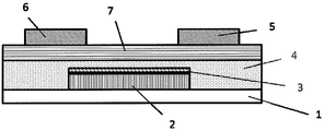
- the transparent organic thin film transistor of this embodiment has a bottom contact type device structure. That is, the first gate electrode 2 is formed on the transparent support substrate 1, the second gate electrode 3 is formed on the first gate electrode 2, and covers the first gate electrode 2 and the second gate electrode 3. A polymer gate insulating layer 4 is formed. A source electrode 5 and a drain electrode 6 are formed on the polymer gate insulating layer 4, and these electrodes are formed at a predetermined interval so as to constitute a channel length of a predetermined distance. Further, an organic semiconductor layer 7 is formed so as to cover the source electrode 5 and the drain electrode 6.
- the transparent support substrate 1 may be any substrate as long as it has transparency and durability to a film forming process as described later.
- a glass substrate a PET (polyethylene terephthalate) film, a PEN (polyethylene naphthalate) film.
- various film substrates such as PC (polycarbonate) film and PES (polyether sulfone) film.
- an inert metal As a material of the first gate electrode 2, an inert metal is used. That is, for example, an electrode material having excellent conductivity such as gold (Au), platinum (Pt), silver (Ag), or the like can be used.
- an inert metal means a metal having a standard electrode potential E ° of 0.6V or more.
- the standard electrode potential means that one of the batteries is a hydrogen electrode represented by a half-cell reaction of the following formula (1), the other is an electrode to be measured, and all the components of the battery are in a standard state.
- Au takes 1.83V
- Pt takes 1.188V
- Ag takes 0.799V.
- the thickness of the first gate electrode 2 is preferably thin in order to have transparency. For example, 5 to 20 nm is preferable, and 5 to 10 nm is more preferable. When it exceeds 20 nm, the transparency tends to be low. If the thickness is less than 5 nm, sufficient conductivity as an electrode tends not to be obtained.
- an active metal is used as the material of the second gate electrode 3. That is, for example, an electrode material having good conductivity such as aluminum (Al), titanium (Ti), chromium (Cr), copper (Cu), or MgAg alloy can be used.
- the active metal means a metal having a standard electrode potential E ° of less than 0.6V.
- Al is -1.676V
- Ti is ⁇ 1.63V
- Cu is 0.52V
- Cr is ⁇ 0. Takes an E ° value of 9V.
- the thickness of the second gate electrode 3 is preferably thin because it has transparency. For example, 1 to 10 nm is preferable, and 1 to 5 nm is more preferable. When it exceeds 10 nm, the transparency tends to be low. When the thickness is less than 1 nm, sufficient conductivity as an electrode tends not to be obtained.
- the reason for using an active metal for the second gate electrode 3 is to form a natural oxide film. That is, as will be described later, since the fluorine-based polymer that is the material of the polymer gate insulating layer 4 reacts with and adheres to the hydroxyl group on the gate electrode, a metal natural oxide film is required for the base. In this case, there is a method of actively oxidizing the active metal by a treatment such as oxygen plasma, but this is not preferable because the number of steps increases accordingly.
- a fluorine-based polymer having sufficient insulation and containing fluorine in the polymer main chain or side chain is used. Since the fluorine-based polymer has a large contact angle with water (because of high water repellency), water molecules and hydroxyl groups on the gate insulating layer are prevented from becoming traps for charge transport, thereby improving transistor performance.
- the contact angle is preferably 80 ° or more, and more preferably 100 ° or more.
- the contact angle with water means the angle formed by the tangent to the surface of the water drop when the water drop is statically placed on a horizontal material surface, and represents the water repellency of the material. It becomes one index.
- the measurement can be performed using a commercially available contact angle meter or the like based on a conventionally known measurement method such as the ⁇ / 2 method, the tangent method, or the curve fitting method.
- an amorphous fluororesin can be used. Since amorphous fluororesin is generally excellent in transparency, it is preferably used in the present invention.
- amorphous fluororesin is generally excellent in transparency, it is preferably used in the present invention.
- “Cytop” (trade name, contact angle with water: 115 °) commercially available from Asahi Glass Co., Ltd.
- “Teflon (registered trademark) AF” trade name, contact angle with water
- the film thickness of the polymer gate insulating layer 4 is preferably 10 to 200 nm, more preferably 20 to 100 nm. If the film thickness is thin, it tends to be difficult to form a flat film. If the film thickness is too thick, the capacitance decreases, and the amount of carriers injected into the organic semiconductor layer 7 described later tends to decrease.
- the electrode material of the source electrode 5 and the drain electrode 6 is not particularly limited as long as it has sufficient conductivity as an electrode.
- Various metal materials such as gold (Au), silver (Ag), titanium (Ti), nickel (Ni) can be used.
- the thickness of the source electrode 5 and the drain electrode 6 can be appropriately adjusted depending on the application. For example, 20 to 100 nm is preferable, and 20 to 50 nm is more preferable. If it exceeds 100 nm, it takes time to form a film, and the process time tends to increase. If it is less than 20 nm, the wiring resistance tends to increase.
- the distance (channel length) L between the source electrode 5 and the drain electrode 6 is preferably 100 ⁇ m or less, and more preferably 50 ⁇ m or less, for example.
- organic semiconductor material of the organic semiconductor layer 7 conventionally known materials can be used.
- P-type low molecular organic semiconductor materials such as pentacene and rubrene
- P-type high molecular organic semiconductor materials such as poly-3-hexylthiophene (P3HT) can be used.
- the film thickness of the organic semiconductor layer 7 is preferably, for example, 10 to 100 nm, more preferably 10 to 60 nm, and most preferably 20 to 40 nm. If it exceeds 100 nm, it takes time to form a film, the process time tends to increase, and the transparency tends to decrease. If the thickness is less than 10 nm, the organic semiconductor material may be island-like and film formation may not be possible, and characteristics may be deteriorated.
- FIG. 2 shows another embodiment of the transparent organic thin film transistor of the present invention.
- an organic semiconductor layer 7 is formed directly on the polymer gate insulating layer 4 without a source electrode or a drain electrode.
- a source electrode 5 and a drain electrode 6 are formed on the semiconductor layer 7.
- the present invention is also applied to a device having such a top contact structure.
- the first gate electrode 2 is formed on the transparent support substrate 1 (first gate electrode forming step).
- the formation of the first gate electrode 2 may be performed in accordance with a conventionally known method.
- the first gate electrode 2 can be formed by a method such as resistance heating vapor deposition, sputtering, or electron beam vapor deposition using the above-described electrode material. .
- the second gate electrode 3 is laminated and formed on the first gate electrode 2 formed on the transparent support substrate 1 (second gate electrode forming step).
- the formation of the second gate electrode 3 may be performed in accordance with a conventionally known method.
- the second gate electrode 3 can be formed by a method such as resistance heating vapor deposition, sputtering, or electron beam vapor deposition using the above-described electrode material. .
- the first gate electrode 2 and the second gate electrode 3 are covered on the surface of the transparent support substrate 1 on which the first gate electrode 2 and the second gate electrode 3 are formed.
- the polymer gate insulating layer 4 is formed (gate insulating layer forming step).
- the polymer gate insulating layer 4 may be formed according to a conventionally known method.
- the polymer gate insulating layer 4 is formed by various coating methods such as a spin coating method, a slit coating method, and a dip coating method using the above-described fluorine-based polymer. be able to.
- the fluoropolymer (the polymer terminal is a silanol group or a carboxyl group) reacts with the surface of the second gate electrode 3 (the hydroxyl group is on the surface).
- the film can be formed by a hydrogen bond or a covalent bond.
- the fluoropolymer is repelled on the gate electrode and film formation is difficult.
- a source electrode 5 and a drain electrode 6 are formed on the polymer gate insulating layer 4 (source / drain electrode forming step).
- the source electrode 5 and the drain electrode 6 may be formed in accordance with a conventionally known method.
- a mask vapor deposition method resistance heating vapor deposition method
- sputtering method electron beam vapor deposition method
- the ink jet method screen printing, spin coating method and the like can be used.
- a coating method such as an inkjet method, screen printing, or spin coating method
- a metal nanoparticle ink such as a silver ink can be used.
- the organic semiconductor layer 7 is formed on the surface of the polymer gate insulating layer 4 on the side where the source electrode 5 and the drain electrode 6 are formed so as to cover the source electrode 5 and the drain electrode 6.
- the organic semiconductor layer 7 may be formed according to a conventionally known method.
- the organic semiconductor layer 7 may be formed by the resistance heating vapor deposition method, the ink jet method, or the like using the organic semiconductor material described above.
- a single crystal thin film is formed by the PVT method (physical vapor transport method), which is disposed on the surface of the polymer gate insulating layer 4 on which the source electrode 5 and the drain electrode 6 are formed,
- the organic semiconductor layer 7 may be used.
- the transparent organic thin film transistor of the present invention can be manufactured.
- the bottom contact structure device (see FIG. 1) has been described above as an example, a device having a top contact structure can be obtained by changing the order of the source / drain electrode formation step and the organic semiconductor layer formation step. (See FIG. 2).
- Example 1 A bottom contact type organic thin film transistor was manufactured through the following steps.
- quartz glass having a thickness of 10 mm ⁇ 10 mm ⁇ 0.7 mm was used as the transparent support substrate. This quartz glass was attached to a resistance heating vapor deposition apparatus, and Au was mask-deposited to form a first gate electrode having a thickness of 10 nm. Next, Al was deposited to 3 nm on the first gate electrode by the same resistance heating vapor deposition apparatus to form a second gate electrode. Next, a fluorine-based polymer (trade name “Cytop”, manufactured by Asahi Glass Co., Ltd.) is used as a polymer insulating material on the surface of the transparent support substrate on which the first and second gate electrodes are formed, and spin coating is performed.
- a fluorine-based polymer trade name “Cytop”, manufactured by Asahi Glass Co., Ltd.
- a gate insulating layer having a thickness of 50 nm was formed by the method. At this time, the process temperature was 120 ° C.
- the transparent support substrate on which the gate insulating layer is formed is mounted in a resistance heating vapor deposition apparatus, and Au having a film thickness of 20 nm and a channel length of 50 ⁇ m is mask-deposited on the upper surface of the gate insulating layer to form a source electrode and a drain electrode. did.
- a single crystal (film thickness: 60 nm) of pentacene (manufactured by Sigma-Aldrich Japan Co., Ltd .: subjected to sublimation purification twice) formed separately by the PVT method is used for the source and drain electrodes formed on the gate insulating layer. Arranged from above, an organic semiconductor layer was formed.
- Example 2 In Example 1, an organic thin film transistor was manufactured in the same manner as in Example 1 except that Au was changed to Ag.
- Example 3 In Example 1, an organic thin film transistor was manufactured in the same manner as Example 1 except that Al was changed to Cr.
- Example 4 In Example 1, an organic thin film transistor was manufactured in the same manner as Example 1 except that Al was changed to Cu.
- Example 5 In Example 1, an organic thin film transistor was manufactured in the same manner as in Example 1 except that Au was changed to Ag and Al was changed to Cr.
- Example 6 An organic thin film transistor was manufactured in the same manner as in Example 1 except that Au was changed to Ag and Al was changed to Cu in Example 1.
- Example 7 the organic thin-film transistor was manufactured similarly to Example 1 except having performed the transparent support substrate with the PEN film (Teijin DuPont Films Co., Ltd. heat resistance 150 degreeC).
- PEN film Teijin DuPont Films Co., Ltd. heat resistance 150 degreeC
- quartz glass having a thickness of 10 mm ⁇ 10 mm ⁇ 0.7 mm was used as the transparent support substrate. This quartz glass was attached to a resistance heating vapor deposition apparatus, and Au was mask-deposited to form a first gate electrode having a thickness of 10 nm. Next, Al was deposited to 3 nm on the first gate electrode by the same resistance heating vapor deposition apparatus to form a second gate electrode. Next, a fluorine-based polymer (trade name “Cytop”, manufactured by Asahi Glass Co., Ltd.) is used as a polymer insulating material on the surface of the transparent support substrate on which the first and second gate electrodes are formed, and spin coating is performed.
- a fluorine-based polymer trade name “Cytop”, manufactured by Asahi Glass Co., Ltd.
- a gate insulating layer having a thickness of 50 nm was formed by the method. At this time, the process temperature was 120 ° C. Next, a single crystal (thickness: 60 nm) of pentacene (manufactured by Sigma Aldrich Japan Co., Ltd .: sublimation purification performed twice) formed separately by the PVT method is disposed on the gate insulating layer, and the organic semiconductor layer Formed. Next, the transparent support substrate on which the organic semiconductor was formed was attached to a resistance heating vapor deposition apparatus, and Au having a film thickness of 20 nm and a channel length of 50 ⁇ m was mask-deposited on the upper surface of the organic semiconductor layer to form a source electrode and a drain electrode. .
- Example 1 an organic thin film transistor was manufactured in the same manner as in Example 1 except that 20 nm of Al was deposited as a gate electrode.
- Example 2 an organic thin film transistor was manufactured in the same manner as in Example 1 except that 20 nm of Au was evaporated as a gate electrode.
- the mobility of the organic thin film transistors of Examples 1 to 8 and Comparative Examples 1 and 2 was measured.
- the mobility was obtained from the gate voltage-drain current characteristics measured with a semiconductor parameter measuring device (manufactured by Agilent).
- the organic thin film transistors of Examples 1 to 8 were flexible transparent devices, and the transistor performance was very good.
- first gate electrode 3 second gate electrode 4: polymer gate insulating layer 5: source electrode 6: drain electrode 7: organic semiconductor layer
Landscapes
- Thin Film Transistor (AREA)
- Electrodes Of Semiconductors (AREA)
Abstract
Description
H++e-=1/2H2 …(1)
例えば、化学便覧(改訂5版、平成16年発行、発行所;丸善株式会社)によれば、Auは1.83V、Ptは1.188V、Agは0.7991VのE゜値をとる。
以下の工程により、ボトムコンタクト型の有機薄膜トランジスタを製造した。
次に、上記第一ゲート電極上に、同じく抵抗加熱蒸着装置により、Alを3nm蒸着して第二ゲート電極を形成した。
次に、透明支持基板上の、上記第一及び第二ゲート電極を形成した側の面に、高分子絶縁材料としてフッ素系ポリマー(商品名「Cytop」、旭硝子株式会社製)を用い、スピンコート法により膜厚50nmのゲート絶縁層を形成した。なお、この時プロセス温度は120℃で行った。
次に、上記ゲート絶縁層を形成した透明支持基板を抵抗加熱蒸着装置に装着し、ゲート絶縁層の上面に膜厚20nm、チャネル長50μmのAuをマスク蒸着して、ソース電極及びドレイン電極を形成した。
次に、別途PVT法で形成した、ペンタセン(シグマ アルドリッチ ジャパン株式会社製:昇華精製を二回実施)の単結晶(膜厚:60nm)を、ゲート絶縁層上に形成したソース電極及びドレイン電極の上から配設し、有機半導体層を形成した。
実施例1において、AuをAgに変更した以外は実施例1と同様にして、有機薄膜トランジスタを製造した。
実施例1において、AlをCrに変更した以外は実施例1と同様にして、有機薄膜トランジスタを製造した。
実施例1において、AlをCuに変更した以外は実施例1と同様にして、有機薄膜トランジスタを製造した。
実施例1において、AuをAgに変更し、AlをCrに変更した以外は実施例1と同様にして、有機薄膜トランジスタを製造した。
実施例1において、AuをAgに変更し、AlをCuに変更した以外は実施例1と同様にして、有機薄膜トランジスタを製造した。
実施例1において、透明支持基板をPENフィルム(帝人デュポンフィルム株式会社製、耐熱性150℃)で行った以外は実施例1と同様にして、有機薄膜トランジスタを製造した。
以下の工程により、トップコンタクト型の有機薄膜トランジスタを製造した。
次に、上記第一ゲート電極上に、同じく抵抗加熱蒸着装置により、Alを3nm蒸着して第二ゲート電極を形成した。
次に、透明支持基板上の、上記第一及び第二ゲート電極を形成した側の面に、高分子絶縁材料としてフッ素系ポリマー(商品名「Cytop」、旭硝子株式会社製)を用い、スピンコート法により膜厚50nmのゲート絶縁層を形成した。なお、この時プロセス温度は120℃で行った。
次に、別途PVT法で形成した、ペンタセン(シグマ アルドリッチ ジャパン株式会社製:昇華精製を二回実施)の単結晶(膜厚:60nm)を、ゲート絶縁層上に配設して、有機半導体層を形成した。
次に、上記有機半導体を形成した透明支持基板を抵抗加熱蒸着装置に装着し、有機半導体層の上面に膜厚20nm、チャネル長50μmのAuをマスク蒸着して、ソース電極及びドレイン電極を形成した。
実施例1において、ゲート電極としてAlを20nm蒸着したこと以外は実施例1と同様にして、有機薄膜トランジスタを製造した。
実施例1において、ゲート電極としてAuを20nm蒸着したこと以外は実施例1と同様にして、有機薄膜トランジスタを製造した。

2:第一ゲート電極
3:第二ゲート電極
4:高分子ゲート絶縁層
5:ソース電極
6:ドレイン電極
7:有機半導体層
Claims (6)
- 透明支持基板上に形成された不活性金属を用いた第一ゲート電極と、前記第一ゲート電極上に形成された活性金属を用いた第二ゲート電極と、前記第二ゲート電極上に形成されたフッ素系ポリマーを用いた高分子ゲート絶縁層と、前記高分子ゲート絶縁層上に形成されたソース電極及びドレイン電極と、前記ソース電極及び前記ドレイン電極上に形成された有機半導体層とを備えたことを特徴とする透明有機薄膜トランジスタ。
- 透明支持基板上に形成された不活性金属を用いた第一ゲート電極と、前記第一ゲート電極上に形成された活性金属を用いた第二ゲート電極と、前記第二ゲート電極上に形成されたフッ素系ポリマーを用いた高分子ゲート絶縁層と、前記高分子ゲート絶縁層上に形成された有機半導体層と、前記有機半導体層上に形成されたソース電極及びドレイン電極とを備えたことを特徴とする透明有機薄膜トランジスタ。
- 前記第一ゲート電極は、Au、Pt、及びAgからなる群から選ばれた1種の材質で構成されたものであり、前記第二ゲート電極は、Al、Ti、Cr、Cu、及びMgAg合金からなる群から選ばれた1種の材質で構成されたものである、請求項1又は2記載の透明有機薄膜トランジスタ。
- 透明支持基板上に不活性金属を用いて第一ゲート電極を形成する工程と、前記第一ゲート電極上に活性金属を用いて第二ゲート電極を形成する工程と、前記第二ゲート電極上にフッ素系ポリマーを用いて高分子ゲート絶縁層を形成する工程と、前記高分子ゲート絶縁層上にソース電極及びドレイン電極を形成する工程と、前記ソース電極及び前記ドレイン電極上に有機半導体層を形成する工程を備えたことを特徴とする透明有機薄膜トランジスタの製造方法。
- 透明支持基板上に不活性金属を用いて第一ゲート電極を形成する工程と、前記第一ゲート電極上に活性金属を用いて第二ゲート電極を形成する工程と、前記第二ゲート電極上にフッ素系ポリマーを用いて高分子ゲート絶縁層を形成する工程と、前記高分子ゲート絶縁層上に有機半導体層を形成する工程と、前記有機半導体層上にソース電極及びドレイン電極を形成する工程を備えたことを特徴とする透明有機薄膜トランジスタの製造方法。
- 前記第一ゲート電極は、Au、Pt、及びAgからなる群から選ばれた1種の材質で構成されたものであり、前記第二ゲート電極は、Al、Ti、Cr、Cu、及びMgAg合金からなる群から選ばれた1種の材質で構成されたものである、請求項4又は5記載の透明有機薄膜トランジスタ。
Priority Applications (2)
| Application Number | Priority Date | Filing Date | Title |
|---|---|---|---|
| US14/651,003 US20150318502A1 (en) | 2013-01-07 | 2013-12-25 | Transparent organic thin-film transistor and method for manufacturing same |
| JP2014549228A JP5787038B2 (ja) | 2013-01-07 | 2013-12-25 | 透明有機薄膜トランジスタ及びその製造方法 |
Applications Claiming Priority (2)
| Application Number | Priority Date | Filing Date | Title |
|---|---|---|---|
| JP2013000466 | 2013-01-07 | ||
| JP2013-000466 | 2013-01-07 |
Publications (1)
| Publication Number | Publication Date |
|---|---|
| WO2014106938A1 true WO2014106938A1 (ja) | 2014-07-10 |
Family
ID=51062258
Family Applications (1)
| Application Number | Title | Priority Date | Filing Date |
|---|---|---|---|
| PCT/JP2013/084619 Ceased WO2014106938A1 (ja) | 2013-01-07 | 2013-12-25 | 透明有機薄膜トランジスタ及びその製造方法 |
Country Status (3)
| Country | Link |
|---|---|
| US (1) | US20150318502A1 (ja) |
| JP (1) | JP5787038B2 (ja) |
| WO (1) | WO2014106938A1 (ja) |
Cited By (1)
| Publication number | Priority date | Publication date | Assignee | Title |
|---|---|---|---|---|
| WO2017159613A1 (ja) * | 2016-03-15 | 2017-09-21 | シャープ株式会社 | アクティブマトリクス基板 |
Families Citing this family (14)
| Publication number | Priority date | Publication date | Assignee | Title |
|---|---|---|---|---|
| US9853230B2 (en) * | 2015-02-17 | 2017-12-26 | Xerox Corporation | Printable nanoparticle conductor ink with improved charge injection |
| US10418622B2 (en) * | 2017-10-26 | 2019-09-17 | GM Global Technology Operations LLC | Battery state estimation control logic and architectures for electric storage systems |
| CN109004006B (zh) * | 2018-07-27 | 2021-10-22 | 京东方科技集团股份有限公司 | 有机发光显示基板及其制作方法、显示装置 |
| US20220140265A1 (en) * | 2019-02-22 | 2022-05-05 | The University Of Tokyo | Organic semiconductor device, method for manufacturing organic semiconductor single crystal film, and method for manufacturing organic semiconductor device |
| US11302996B2 (en) | 2019-08-19 | 2022-04-12 | GM Global Technology Operations LLC | Battery modules with integrated interconnect board assemblies having cell tab comb features |
| US11207982B2 (en) | 2019-12-11 | 2021-12-28 | GM Global Technology Operations LLC | Electronic power module assemblies and control logic with direct-cooling heat pipe systems |
| US11375642B2 (en) | 2019-12-23 | 2022-06-28 | GM Global Technology Operations LLC | Electronic power module assemblies and control logic with direct-cooling vapor chamber systems |
| US11801574B2 (en) | 2020-03-06 | 2023-10-31 | GM Global Technology Operations LLC | Welding systems and methods with knurled weld interfaces for metallic workpieces |
| US11387525B2 (en) | 2020-03-09 | 2022-07-12 | GM Global Technology Operations LLC | Two-stage plunger press systems and methods for forming battery cell tabs |
| US11600842B2 (en) | 2020-03-16 | 2023-03-07 | GM Global Technology Operations LLC | Multistage plunger press systems and methods with interlocking fingers for forming battery cell tabs |
| US11804639B2 (en) | 2020-07-23 | 2023-10-31 | GM Global Technology Operations LLC | Multistage plunger systems and methods for forming battery cell tabs |
| US11799149B2 (en) | 2020-08-26 | 2023-10-24 | GM Global Technology Operations LLC | Energy storage assembly |
| US11581618B2 (en) | 2020-11-18 | 2023-02-14 | GM Global Technology Operations LLC | Thermomechanical fuses for heat propagation mitigation of electrochemical devices |
| US12132010B2 (en) | 2021-04-08 | 2024-10-29 | GM Global Technology Operations LLC | Metal-coated, polymer-encapsulated electronics modules and methods for making the same |
Citations (7)
| Publication number | Priority date | Publication date | Assignee | Title |
|---|---|---|---|---|
| JP2006005041A (ja) * | 2004-06-16 | 2006-01-05 | Toshiba Corp | 有機半導体素子とその製造方法 |
| JP2006073908A (ja) * | 2004-09-06 | 2006-03-16 | Sony Corp | 薄膜型電界効果トランジスタ、薄膜型電界効果トランジスタの製造方法、アクティブマトリクス回路および液晶表示装置 |
| JP2006279053A (ja) * | 2005-03-29 | 2006-10-12 | Samsung Electronics Co Ltd | 有機薄膜トランジスタ表示板及びその製造方法 |
| JP2010056303A (ja) * | 2008-08-28 | 2010-03-11 | Epson Imaging Devices Corp | 光センサ及びこの光センサを使用した液晶表示装置 |
| JP2010098280A (ja) * | 2008-02-22 | 2010-04-30 | Toppan Printing Co Ltd | 透明薄膜トランジスタ及び画像表示装置 |
| WO2010101224A1 (ja) * | 2009-03-06 | 2010-09-10 | 国立大学法人九州工業大学 | 有機半導体材料および有機薄膜トランジスタ |
| JP2012169419A (ja) * | 2011-02-14 | 2012-09-06 | Nippon Hoso Kyokai <Nhk> | 有機薄膜トランジスタ |
Family Cites Families (18)
| Publication number | Priority date | Publication date | Assignee | Title |
|---|---|---|---|---|
| US6365917B1 (en) * | 1998-11-25 | 2002-04-02 | Semiconductor Energy Laboratory Co., Ltd. | Semiconductor device |
| US6259138B1 (en) * | 1998-12-18 | 2001-07-10 | Semiconductor Energy Laboratory Co., Ltd. | Semiconductor device having multilayered gate electrode and impurity regions overlapping therewith |
| JP4152665B2 (ja) * | 2001-07-11 | 2008-09-17 | 株式会社半導体エネルギー研究所 | 発光装置及びその作製方法 |
| US6933568B2 (en) * | 2002-05-17 | 2005-08-23 | Samsung Electronics Co., Ltd. | Deposition method of insulating layers having low dielectric constant of semiconductor device, a thin film transistor substrate using the same and a method of manufacturing the same |
| JP4831954B2 (ja) * | 2003-11-14 | 2011-12-07 | 株式会社半導体エネルギー研究所 | 表示装置の作製方法 |
| US20090026443A1 (en) * | 2005-03-15 | 2009-01-29 | Pioneer Corporation | Organic thin-film transistor and method of manufacture thereof |
| EP1830422A3 (en) * | 2006-03-03 | 2012-03-07 | Semiconductor Energy Laboratory Co., Ltd. | Light emitting device and electronic device |
| JP2009212389A (ja) * | 2008-03-05 | 2009-09-17 | Fujifilm Corp | 透明有機薄膜トランジスタ |
| JP2009224689A (ja) * | 2008-03-18 | 2009-10-01 | Sanyo Electric Co Ltd | 有機トランジスタ及びその製造方法 |
| JP2009238968A (ja) * | 2008-03-27 | 2009-10-15 | Brother Ind Ltd | 有機薄膜トランジスタの製造方法、およびそれを用いた有機薄膜トランジスタ |
| JP2011012001A (ja) * | 2009-07-01 | 2011-01-20 | Sony Corp | アンタントレン系化合物及び半導体装置 |
| KR101716471B1 (ko) * | 2010-06-07 | 2017-03-28 | 삼성디스플레이 주식회사 | 유기 발광 표시 장치 및 그 제조 방법 |
| JP6061858B2 (ja) * | 2010-10-07 | 2017-01-18 | ジョージア・テック・リサーチ・コーポレーション | 電界効果トランジスタおよびその製造方法 |
| TWM406254U (en) * | 2010-12-09 | 2011-06-21 | Chunghwa Picture Tubes Ltd | Thin film transistor having schottky barrier |
| KR20140052016A (ko) * | 2011-08-12 | 2014-05-02 | 바스프 에스이 | 카르바졸로카르바졸-비스(디카르복스이미드) 및 반도체로서의 그의 용도 |
| US8912535B2 (en) * | 2012-04-13 | 2014-12-16 | Georgia Tech Research Corporation | Naphthalene-diimide-heterocycle-naphthalene diimide oligomers as organic semiconductors and transistors therefrom |
| KR101938761B1 (ko) * | 2012-05-23 | 2019-01-16 | 삼성디스플레이 주식회사 | 박막 트랜지스터 어레이 기판, 이를 포함하는 유기 발광 표시 장치 및 그 제조 방법 |
| KR20140010306A (ko) * | 2012-07-16 | 2014-01-24 | 삼성디스플레이 주식회사 | 유기 발광 표시 장치 및 유기 발광 표시 장치의 제조 방법 |
-
2013
- 2013-12-25 WO PCT/JP2013/084619 patent/WO2014106938A1/ja not_active Ceased
- 2013-12-25 US US14/651,003 patent/US20150318502A1/en not_active Abandoned
- 2013-12-25 JP JP2014549228A patent/JP5787038B2/ja not_active Expired - Fee Related
Patent Citations (7)
| Publication number | Priority date | Publication date | Assignee | Title |
|---|---|---|---|---|
| JP2006005041A (ja) * | 2004-06-16 | 2006-01-05 | Toshiba Corp | 有機半導体素子とその製造方法 |
| JP2006073908A (ja) * | 2004-09-06 | 2006-03-16 | Sony Corp | 薄膜型電界効果トランジスタ、薄膜型電界効果トランジスタの製造方法、アクティブマトリクス回路および液晶表示装置 |
| JP2006279053A (ja) * | 2005-03-29 | 2006-10-12 | Samsung Electronics Co Ltd | 有機薄膜トランジスタ表示板及びその製造方法 |
| JP2010098280A (ja) * | 2008-02-22 | 2010-04-30 | Toppan Printing Co Ltd | 透明薄膜トランジスタ及び画像表示装置 |
| JP2010056303A (ja) * | 2008-08-28 | 2010-03-11 | Epson Imaging Devices Corp | 光センサ及びこの光センサを使用した液晶表示装置 |
| WO2010101224A1 (ja) * | 2009-03-06 | 2010-09-10 | 国立大学法人九州工業大学 | 有機半導体材料および有機薄膜トランジスタ |
| JP2012169419A (ja) * | 2011-02-14 | 2012-09-06 | Nippon Hoso Kyokai <Nhk> | 有機薄膜トランジスタ |
Cited By (1)
| Publication number | Priority date | Publication date | Assignee | Title |
|---|---|---|---|---|
| WO2017159613A1 (ja) * | 2016-03-15 | 2017-09-21 | シャープ株式会社 | アクティブマトリクス基板 |
Also Published As
| Publication number | Publication date |
|---|---|
| JPWO2014106938A1 (ja) | 2017-01-19 |
| US20150318502A1 (en) | 2015-11-05 |
| JP5787038B2 (ja) | 2015-09-30 |
Similar Documents
| Publication | Publication Date | Title |
|---|---|---|
| JP5787038B2 (ja) | 透明有機薄膜トランジスタ及びその製造方法 | |
| JP5499422B2 (ja) | 有機半導体材料、有機半導体膜、有機薄膜トランジスタ及び有機薄膜トランジスタの製造方法 | |
| US7382040B2 (en) | Organic field effect transistor and display using same | |
| CN102867914B (zh) | 电子器件和半导体器件的制造方法 | |
| CN108538919A (zh) | 薄膜晶体管 | |
| CN103403903A (zh) | 场效应晶体管及其制造方法 | |
| TW200843118A (en) | Ambipolar transistor design | |
| TW201640684A (zh) | 薄膜電晶體、薄膜電晶體之製造方法及使用薄膜電晶體之影像顯示裝置 | |
| WO2016115824A1 (zh) | 薄膜晶体管、阵列基板及其制作方法 | |
| JP4826074B2 (ja) | 電界効果型トランジスタ | |
| CN106952962A (zh) | 薄膜晶体管和阵列基板 | |
| WO2010053171A1 (ja) | スイッチング素子及びその製造方法 | |
| US20170200889A1 (en) | Method for manufacturing transistor according to selective printing of dopant | |
| JP6191235B2 (ja) | 有機トランジスタ及びその製造方法 | |
| US20100041861A1 (en) | Semiconducting polymers | |
| US7872258B2 (en) | Organic thin-film transistors | |
| JP5066846B2 (ja) | 有機トランジスタおよびその製造方法 | |
| JP2010118445A (ja) | 薄膜トランジスタ及びその製造方法 | |
| JP2019153653A (ja) | 有機半導体装置 | |
| JP2010258126A (ja) | 薄膜トランジスタ及びその製造方法 | |
| US20120132991A1 (en) | Organic thin-film transistor, and process for production thereof | |
| JP6369098B2 (ja) | 薄膜トランジスタの製造方法 | |
| JP2020088026A (ja) | 有機半導体薄膜トランジスタ素子 | |
| JP2008300546A (ja) | 有機薄膜トランジスタ | |
| JP2008300419A (ja) | 有機薄膜トランジスタ |
Legal Events
| Date | Code | Title | Description |
|---|---|---|---|
| 121 | Ep: the epo has been informed by wipo that ep was designated in this application |
Ref document number: 13869975 Country of ref document: EP Kind code of ref document: A1 |
|
| ENP | Entry into the national phase |
Ref document number: 2014549228 Country of ref document: JP Kind code of ref document: A |
|
| WWE | Wipo information: entry into national phase |
Ref document number: 14651003 Country of ref document: US |
|
| NENP | Non-entry into the national phase |
Ref country code: DE |
|
| 122 | Ep: pct application non-entry in european phase |
Ref document number: 13869975 Country of ref document: EP Kind code of ref document: A1 |