WO2014103671A1 - 発光装置 - Google Patents
発光装置 Download PDFInfo
- Publication number
- WO2014103671A1 WO2014103671A1 PCT/JP2013/082911 JP2013082911W WO2014103671A1 WO 2014103671 A1 WO2014103671 A1 WO 2014103671A1 JP 2013082911 W JP2013082911 W JP 2013082911W WO 2014103671 A1 WO2014103671 A1 WO 2014103671A1
- Authority
- WO
- WIPO (PCT)
- Prior art keywords
- light
- phosphor
- light emitting
- phosphor layer
- emitting device
- Prior art date
- Legal status (The legal status is an assumption and is not a legal conclusion. Google has not performed a legal analysis and makes no representation as to the accuracy of the status listed.)
- Ceased
Links
Images







Classifications
-
- C—CHEMISTRY; METALLURGY
- C09—DYES; PAINTS; POLISHES; NATURAL RESINS; ADHESIVES; COMPOSITIONS NOT OTHERWISE PROVIDED FOR; APPLICATIONS OF MATERIALS NOT OTHERWISE PROVIDED FOR
- C09K—MATERIALS FOR MISCELLANEOUS APPLICATIONS, NOT PROVIDED FOR ELSEWHERE
- C09K11/00—Luminescent materials, e.g. electroluminescent or chemiluminescent
- C09K11/08—Luminescent materials, e.g. electroluminescent or chemiluminescent containing inorganic luminescent materials
- C09K11/77—Luminescent materials, e.g. electroluminescent or chemiluminescent containing inorganic luminescent materials containing rare earth metals
- C09K11/7708—Vanadates; Chromates; Molybdates; Tungstates
-
- A—HUMAN NECESSITIES
- A01—AGRICULTURE; FORESTRY; ANIMAL HUSBANDRY; HUNTING; TRAPPING; FISHING
- A01G—HORTICULTURE; CULTIVATION OF VEGETABLES, FLOWERS, RICE, FRUIT, VINES, HOPS OR SEAWEED; FORESTRY; WATERING
- A01G7/00—Botany in general
- A01G7/04—Electric or magnetic or acoustic treatment of plants for promoting growth
- A01G7/045—Electric or magnetic or acoustic treatment of plants for promoting growth with electric lighting
-
- C—CHEMISTRY; METALLURGY
- C09—DYES; PAINTS; POLISHES; NATURAL RESINS; ADHESIVES; COMPOSITIONS NOT OTHERWISE PROVIDED FOR; APPLICATIONS OF MATERIALS NOT OTHERWISE PROVIDED FOR
- C09K—MATERIALS FOR MISCELLANEOUS APPLICATIONS, NOT PROVIDED FOR ELSEWHERE
- C09K11/00—Luminescent materials, e.g. electroluminescent or chemiluminescent
- C09K11/08—Luminescent materials, e.g. electroluminescent or chemiluminescent containing inorganic luminescent materials
- C09K11/77—Luminescent materials, e.g. electroluminescent or chemiluminescent containing inorganic luminescent materials containing rare earth metals
- C09K11/7728—Luminescent materials, e.g. electroluminescent or chemiluminescent containing inorganic luminescent materials containing rare earth metals containing europium
- C09K11/77348—Silicon Aluminium Nitrides or Silicon Aluminium Oxynitrides
-
- H—ELECTRICITY
- H10—SEMICONDUCTOR DEVICES; ELECTRIC SOLID-STATE DEVICES NOT OTHERWISE PROVIDED FOR
- H10H—INORGANIC LIGHT-EMITTING SEMICONDUCTOR DEVICES HAVING POTENTIAL BARRIERS
- H10H20/00—Individual inorganic light-emitting semiconductor devices having potential barriers, e.g. light-emitting diodes [LED]
- H10H20/80—Constructional details
- H10H20/85—Packages
- H10H20/851—Wavelength conversion means
- H10H20/8511—Wavelength conversion means characterised by their material, e.g. binder
- H10H20/8512—Wavelength conversion materials
-
- H—ELECTRICITY
- H10—SEMICONDUCTOR DEVICES; ELECTRIC SOLID-STATE DEVICES NOT OTHERWISE PROVIDED FOR
- H10H—INORGANIC LIGHT-EMITTING SEMICONDUCTOR DEVICES HAVING POTENTIAL BARRIERS
- H10H20/00—Individual inorganic light-emitting semiconductor devices having potential barriers, e.g. light-emitting diodes [LED]
- H10H20/80—Constructional details
- H10H20/85—Packages
- H10H20/851—Wavelength conversion means
- H10H20/8511—Wavelength conversion means characterised by their material, e.g. binder
- H10H20/8512—Wavelength conversion materials
- H10H20/8513—Wavelength conversion materials having two or more wavelength conversion materials
-
- H—ELECTRICITY
- H10—SEMICONDUCTOR DEVICES; ELECTRIC SOLID-STATE DEVICES NOT OTHERWISE PROVIDED FOR
- H10H—INORGANIC LIGHT-EMITTING SEMICONDUCTOR DEVICES HAVING POTENTIAL BARRIERS
- H10H20/00—Individual inorganic light-emitting semiconductor devices having potential barriers, e.g. light-emitting diodes [LED]
- H10H20/80—Constructional details
- H10H20/85—Packages
- H10H20/851—Wavelength conversion means
- H10H20/8516—Wavelength conversion means having a non-uniform spatial arrangement or non-uniform concentration, e.g. patterned wavelength conversion layer or wavelength conversion layer with a concentration gradient
-
- H—ELECTRICITY
- H10—SEMICONDUCTOR DEVICES; ELECTRIC SOLID-STATE DEVICES NOT OTHERWISE PROVIDED FOR
- H10W—GENERIC PACKAGES, INTERCONNECTIONS, CONNECTORS OR OTHER CONSTRUCTIONAL DETAILS OF DEVICES COVERED BY CLASS H10
- H10W90/00—Package configurations
-
- H—ELECTRICITY
- H10—SEMICONDUCTOR DEVICES; ELECTRIC SOLID-STATE DEVICES NOT OTHERWISE PROVIDED FOR
- H10W—GENERIC PACKAGES, INTERCONNECTIONS, CONNECTORS OR OTHER CONSTRUCTIONAL DETAILS OF DEVICES COVERED BY CLASS H10
- H10W90/00—Package configurations
- H10W90/701—Package configurations characterised by the relative positions of pads or connectors relative to package parts
- H10W90/751—Package configurations characterised by the relative positions of pads or connectors relative to package parts of bond wires
- H10W90/753—Package configurations characterised by the relative positions of pads or connectors relative to package parts of bond wires between laterally-adjacent chips
-
- Y—GENERAL TAGGING OF NEW TECHNOLOGICAL DEVELOPMENTS; GENERAL TAGGING OF CROSS-SECTIONAL TECHNOLOGIES SPANNING OVER SEVERAL SECTIONS OF THE IPC; TECHNICAL SUBJECTS COVERED BY FORMER USPC CROSS-REFERENCE ART COLLECTIONS [XRACs] AND DIGESTS
- Y02—TECHNOLOGIES OR APPLICATIONS FOR MITIGATION OR ADAPTATION AGAINST CLIMATE CHANGE
- Y02P—CLIMATE CHANGE MITIGATION TECHNOLOGIES IN THE PRODUCTION OR PROCESSING OF GOODS
- Y02P60/00—Technologies relating to agriculture, livestock or agroalimentary industries
- Y02P60/14—Measures for saving energy, e.g. in green houses
Definitions
- the present invention relates to a light emitting device.
- Producers and supplies of plants such as vegetables and fruits may decrease due to climate change and pest damage.
- emphasis has been placed on improving food safety and food self-sufficiency, and it is desirable to be able to provide safe plants stably. Therefore, technology for growing plants in factory facilities without using sunlight has been developed.
- a light emitting element such as an LED (light emitting diode) is used as a light source of a plant growing lighting device.
- light having peak wavelengths wavelengths at which the relative radiation intensity becomes maximum in the spectrum distribution
- light having a peak wavelength in the wavelength range of 600 nm to 700 nm required for photosynthesis and the wavelength range of 400 nm to 480 nm required for normal leaf morphogenesis is effective.
- Patent Document 1 discloses an illumination device including a plurality of light emitting elements having peak wavelengths in different wavelength regions. According to this configuration, it is possible to irradiate a plant with light having peak wavelengths in a plurality of wavelength regions.
- the cost increases due to the complexity of the drive circuit and the increase in the number of parts due to the electrical characteristics and temperature characteristics of each light emitting element.
- light emitting devices having a peak wavelength in the wavelength range of 600 nm to 700 nm are often made of a compound such as GaAlP that is weak in humidity, and it is necessary to take measures against humidity in a high humidity environment such as a plant growing environment.
- Patent Document 2 discloses an illumination device including a blue LED, a GGG (gadolinium gallium garnet) phosphor (far red phosphor), and a red phosphor. According to this configuration, far red light and red light are emitted from the far red phosphor and the red phosphor when excited by the excitation light of the blue LED in addition to the blue light.
- GGG gallium gallium garnet
- red phosphor far red phosphor
- An object of the present invention is to provide an inexpensive light-emitting device that can grow plants efficiently.
- a light-emitting device of the present invention includes a light-emitting element that emits excitation light, and a far-red fluorescent light that emits light having a peak wavelength in the range of 700 nm to 800 nm when excited by the excitation light of the light-emitting element.
- the median diameter of the far-red phosphor is in the range of 1 ⁇ m to 20 ⁇ m.
- the light-emitting device having the above-described structure preferably further includes a red phosphor that emits light having a peak wavelength in the range of 600 nm to 700 nm when excited by the excitation light of the light-emitting element.
- the phosphor layer including the far red phosphor and the red phosphor may be formed so that absorption of light emitted from the red phosphor by the far red phosphor is suppressed. desirable.
- the phosphor layer includes a first phosphor layer in which the concentration of the red phosphor is higher than the concentration of the far red phosphor and the concentration of the far red phosphor is that of the red phosphor. It is desirable to have a second phosphor layer that is higher than the concentration.
- the first phosphor layer is disposed at a position away from the second phosphor layer in the excitation light irradiation direction of the light-emitting element.
- the first phosphor layer and the second phosphor layer are arranged in a direction perpendicular to the emission direction of the excitation light of the light emitting element.
- the first phosphor layer and the second phosphor layer are directed from one phosphor layer of the first phosphor layer and the second phosphor layer to the other phosphor layer. It is desirable to arrange in a top view band shape so as to suppress the amount of light irradiated.
- the specific gravity of the far red phosphor is greater than the specific gravity of the red phosphor.
- the far red phosphor has a specific gravity of 6.5 to 7.5 and the red phosphor has a specific gravity of 2.0 to 4.0.
- the light emitting element emits excitation light to the first phosphor layer and the second phosphor layer to emit excitation light to the second phosphor layer. It is desirable that the first light emitting element group and the second light emitting element group can be individually controlled to be turned on / off.
- the phosphor and / or the sediment having a wavelength different from the peak wavelength of the light emitted from the far red phosphor and the red phosphor when excited by the excitation light of the light emitting element. It is desirable to contain an inhibitor.
- the red phosphor is CaAlSiN 3 : Eu, (Sr, Ca) AlSiN 3 : Eu, 3.5MgO ⁇ 0.5MgF 2 ⁇ GeO 2 : Mn, (Ca, Sr) S. : (Eu, Ce, K), M 2 Si 5 N 8 : It is desirable to include at least one red phosphor having a component of Eu (M is at least one element selected from Ca, Sr, and Ba). .
- the red phosphor emits light having a peak wavelength near 620 nm when excited by excitation light of the light emitting element.
- the far-red phosphor is a phosphor represented by the chemical formula (Ln 1-x Cr x ) 3 M 5 O 12 (Ln is at least one selected from Y, La, Gd, and Lu). It is desirable that the element, M is at least one element selected from Al, Ga and In, and x is a number satisfying the following formula 0.005 ⁇ x ⁇ 0.2.
- the light-emitting device having the above configuration is used for plant cultivation.
- the far-red phosphor that is excited by the excitation light of the light-emitting element and emits far-red light is optimized, and the median diameter of the far-red phosphor is optimized to 1 ⁇ m to 20 ⁇ m.
- the crystal grows moderately, so that the crystal growth is not insufficient or abnormally grown coarse particles are not generated, and the light emitted from the light emitting device becomes brighter. Plant growth efficiency is improved.
- a far red phosphor or a phosphor layer containing a red phosphor is formed so that absorption of light emitted from the red phosphor by the far red phosphor is suppressed, and the light emitted from the light emitting device becomes brighter.
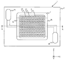
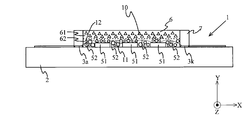
- the top view which shows the light-emitting device of 1st Embodiment. 1 is a side view of the light emitting device shown in FIG.
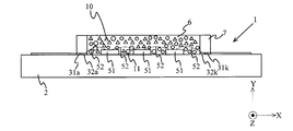
- the top view which shows the light-emitting device of 2nd Embodiment. 5 is a side view of the light emitting device shown in FIG.
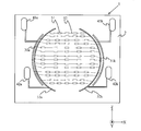
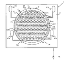
- the top view which shows the light-emitting device of 3rd Embodiment. 7 is a side view of the light emitting device shown in FIG.
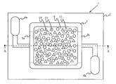
- FIG. 11 is a side view of the light emitting device shown in FIG.
- the top view which shows the light-emitting device of 5th Embodiment.
- 14 is a side view of the light emitting device shown in FIG.
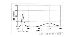
- the top view which shows LED mounted on a cup in 6th Embodiment The figure which shows the spectrum distribution of the emitted light of the light-emitting device shown in 5th Embodiment.
- Light acts as a source of stimulation and information such as germination, flowering and stem elongation.
- the photosynthetic action of plants is performed by absorption of light by chlorophyll (chlorophyll).
- chlorophyll chlorophyll
- the light in the first region is light necessary for normal morphogenesis such as leaves
- the light in the second region is light necessary for photosynthesis.
- far-red light is required for internode elongation and germination.
- the phytochrome contained in the plant is between a phytochrome Pr type having a photoreceptive range for red light having a wavelength in the range of 600 nm to 700 nm and a phytochrome Pfr type having a photoreceptive range for far red light having a wavelength in the range of 700 nm to 800 nm. Reversibly photoconverts and accepts each light. That is, by adjusting the light to be received, photomorphogenic functions such as internode elongation and germination are suppressed or promoted.
- the extension action depends on the ratio R / FR of the light intensity (R) of red light and the light intensity (FR) of far red light, and the ratio of red light and far red light can be selectively or arbitrarily adjusted. It is possible to control elongation suppression and elongation promotion. Specifically, when the ratio R / FR of the light intensity (R) of red light and the light intensity (FR) of far-red light is higher than the natural light environment (1.1 to 1.2), the expansion is suppressed, and when the ratio is low, the expansion is suppressed. Is promoted.
- FIG. 1 is a top view showing the light emitting device of the first embodiment.
- FIG. 2 is a side view of the light emitting device shown in FIG.
- FIG. 3 is a top view showing the LED mounted on the substrate in the first embodiment.
- FIG. 4 is a side view showing the LED mounted on the substrate in the first embodiment.
- FIGS. 3 and 4 are the same as FIGS. 1 and 2, respectively, except for the phosphor layer and the resin frame.
- FIGS. 2, 3 and 4 For simplification of the drawing, the LED shown in FIGS. 2, 3 and 4 is not shown in FIG. 1, but the silicone resin described later has transparency, and the LED is visible in FIG. There may be. The same applies to FIG. 5, FIG. 7, FIG. 11, FIG.
- the light-emitting device 1 of this embodiment includes a substrate 2, a wiring pattern 3, an electrode land 4, a light-emitting element (LED) 5, a phosphor layer 6, and a resin frame 7.
- the substrate 2 is a ceramic substrate having a substantially rectangular shape when viewed from above.
- substrate 2 is not restricted to a ceramic substrate, A glass substrate, a printed circuit board, etc. may be sufficient.
- the wiring patterns 3 (3a, 3k) are formed on the substrate 2 by a screen printing method or the like so as to face each other.
- Each of the wiring patterns 3a and 3k has a substantially rectangular shape when viewed from above. Note that the shape of the wiring pattern is not limited to this, and for example, an arc shape in which a part of the ring is cut out in a top view may be configured.
- the light emitting device 1 is a so-called chip-on-board type light emitting device.
- the electrode land 4 (4a, 4k) is formed on the substrate 2 as a power supply electrode using a material such as Ag-Pt by a screen printing method or the like.
- the electrode land 4a is an anode electrode land
- the electrode land 4k is a cathode electrode land.
- the electrode land 4a is connected to the wiring pattern 3a via a lead wire
- the electrode land 4k is connected to the wiring pattern 3k via a lead wire.
- the LED 5 is a light emitting element (semiconductor light emitting element) mounted on the substrate 2.
- the LED 5 emits light having a peak wavelength in the wavelength range of 400 nm to 480 nm, more specifically in the vicinity of a wavelength of 450 nm, and is composed of a gallium nitride blue LED chip 51 with good temperature and humidity characteristics.
- the number of LED chips 51 constituting the LED 5 is not particularly limited, and may be constituted by a single LED chip 51, but in the present embodiment, it is constituted by a plurality of LED chips 51.
- the LED 5 is configured by arranging six LED chips 51 electrically connected in series so as to be substantially parallel to one side (X direction) of the substrate 2 in parallel and electrically connecting each column in parallel. . That is, the LED 5 includes a total of 18 LED chips 51. Note that the electrical connection method and arrangement of the LED chips 51 in the LEDs 5 are not limited to this.
- the LED chips 51 in each row are connected to each other by a conductive wire 52, and the LED chips 51 at both ends of each row are connected to the wiring pattern 3 by a conductive wire 52.
- the LED 5 emits light having a peak wavelength in the wavelength range of 400 nm to 480 nm.
- the present invention is not limited to this, and light having a peak wavelength in a region less than 400 nm including ultraviolet light is used. It is good also as emitting light.
- the phosphor layer 6 is a resin layer that fills the inside of a resin frame 7 described later and covers the LED 5.
- the phosphor layer 6 is excited by light (excitation light) emitted from the LED 5 and emits light having a peak wavelength in a predetermined range.
- the phosphor layer 6 is a far-red phosphor (denoted by reference numeral 11 in FIG. 1 or the like) that emits light having a peak wavelength in the wavelength range of 700 nm to 800 nm when excited by the excitation light of the LED 5 on a sealing resin made of silicone resin. (Phosphor shown by ⁇ mark).
- a gadolinium / gallium / garnet-based far-red phosphor that emits light having a peak wavelength near 715 nm when excited by the excitation light of the LED 5 is used as the far-red phosphor.
- the type is not limited to this.
- the far-red phosphor is Gd 3 Ga 5 O 12 : Cr.
- the particle diameter of the far red phosphor is preferably in the range of 1 to 20 ⁇ m median diameter, more preferably in the range of 2 to 18 ⁇ m median diameter, and in the range of 3 to 15 ⁇ m median diameter. Most preferably. This is because if the median diameter of the gadolinium / gallium / garnet phosphor exceeds 20 ⁇ m, abnormally grown coarse particles are likely to be generated, making it difficult to use.
- the resin frame 7 is a resin surrounding the phosphor layer 6 so that the phosphor layer 6 does not leak out from a certain range.
- the resin frame 7 is formed in a rectangular ring shape so as to cover the wiring pattern 3 (in FIG. 1, the wiring pattern 3 is indicated by a broken line because it is covered by the resin frame 7).
- the shape of the resin frame is not limited to this, and may be a shape that can cover the wiring pattern 3 according to the shape of the wiring pattern 3, for example. That is, as described above, if the wiring pattern 3 has an arc shape obtained by cutting out a part of the ring, the resin frame 7 may be formed in an annular shape.
- the LED 5 is disposed inside the resin frame 7, and the electrode land 4 is disposed outside the resin frame 7.
- the light emitted from the LED 5 may be referred to as blue light
- the light emitted from the far red phosphor 11 when excited by the excitation light of the LED 5 may be referred to as far red light.
- the ratio of the light intensity of blue light and far red light when the LED 5 is caused to emit light can be adjusted by adjusting the content ratio of the far red phosphor 11 in the sealing resin.
- the light emitted from the light emitting device 1 is blue light and far red light.
- far-red light has a very low relative visibility and is difficult for the human eye to sense brightness.
- Blue light has a high visual acuity several tens of times compared to far-red light. It looks blue light to the human eye. It is difficult to look directly at the light, and a defense reaction such as turning away the eyes occurs. Therefore, compared with a light source that emits only far-red light, adverse effects on the human eye due to far-red light can be prevented.
- the far-red phosphor that is excited by the excitation light of the light emitting element and emits far-red light is optimized, and the median diameter of the far-red phosphor is optimized to 1 ⁇ m to 20 ⁇ m.
- Such far-red phosphors do not have insufficient crystal growth or have abnormally grown coarse particles, and the light emitted from the light-emitting device of the present embodiment is brightened to improve plant growth efficiency. To do.
- the light-emitting device a light-emitting device that emits far-red light with an easy configuration, and can perform flowering control such as promotion of flowering of plants and suppression of flowering.
- flowering control such as promotion of flowering of plants and suppression of flowering.
- the convenience of use is high. Therefore, it can be suitably used as an artificial light source used in a completely closed factory, and can also be used as an auxiliary light source in a plant factory using sunlight.
- the light emitting element is an LED element that emits light having a peak wavelength in the range of 400 nm to 480 nm, the plant can be irradiated with blue light important for plant growth.
- the number of LEDs 5 may be one.
- there are a plurality of LEDs 5 and the connection method may be serial connection or parallel connection.
- At least one light emitting device 1 is mounted on the mounting substrate.
- the phosphor layer 6 is a far-red phosphor that emits light having a peak wavelength in the wavelength range of 700 nm to 800 nm when excited by the excitation light of the LED 5 and the excitation light of the LED 5.
- a red phosphor (CaAlSiN 3 : Eu-based phosphor) that emits light having a peak wavelength around 650 nm when excited may be mixed.
- a red phosphor (Sr, Ca) AlSiN 3 : Eu phosphor that emits light having a peak wavelength near 620 nm when excited by the excitation light of the LED 5 may be mixed.
- a part of the red light (red light having a wavelength of about 620 nm) emitted from the red phosphor contained in the phosphor layer 6 is a mixture of the far red phosphor 11 (shown by a circle in FIG. 1 and the like). (Phosphor).
- the phosphor layer 6 contains a red phosphor (Sr, Ca) AlSiN 3 : Eu-based phosphor) that emits light having a peak wavelength in the vicinity of a wavelength of 620 nm, a decrease in light intensity of red light is minimized. Can be suppressed.
- the phosphor layer 6 contains a red phosphor will be described.
- FIG. 5 is a top view showing the light emitting device of the second embodiment.
- FIG. 6 is a side view of the light emitting device shown in FIG. Since the LED mounted on the substrate is the same as that of the first embodiment, the illustration is omitted. A part of the description of the same configuration as that of the first embodiment is omitted.
- the phosphor layer 6 is a resin layer that fills the inside of a resin frame 7 described later and covers the LED 5.
- the phosphor layer 6 is excited by light (excitation light) emitted from the LED 5 and emits light having a peak wavelength in a predetermined range.
- the phosphor layer 6 includes a first phosphor layer 61 and a second phosphor layer 62.
- the first phosphor layer 61 is made of a sealing resin made of silicone resin containing the first phosphor 10 (phosphor indicated by ⁇ in FIG. 5 and the like), and the second phosphor layer 62 is made of silicone resin.
- the second phosphor 11 (phosphor indicated by a circle in FIG. 5) is contained in the sealing resin made of.
- the first phosphor layer 61 and the second phosphor layer 62 are stacked in two layers in the direction perpendicular to the mounting surface of the substrate 2 (Y direction), and the first phosphor layer 61 is the second phosphor. Formed above layer 62.
- the first phosphor 10 is a red phosphor that emits light having a peak wavelength in the wavelength range of 600 nm to 700 nm when excited by the excitation light of the LED 5.
- the second phosphor 11 is a far red phosphor that is excited by the excitation light of the LED 5 and emits light having a peak wavelength in the wavelength range of 700 nm to 800 nm.
- a CaAlSiN 3 : Eu-based phosphor that emits light having a peak wavelength near 650 nm when excited by the excitation light of the LED 5 is used as the red phosphor, but the type of the red phosphor is not limited thereto. It is not something that can be done.
- a gadolinium gallium garnet-based far red phosphor that emits light having a peak wavelength near 715 nm when excited by the excitation light of the LED 5 is used as the far red phosphor. It is not limited to this.
- the particle diameter of the far red phosphor is preferably in the range of 1 to 20 ⁇ m median diameter, more preferably in the range of 2 to 18 ⁇ m median diameter, and in the range of 3 to 15 ⁇ m median diameter. Most preferably. This is because if the median diameter of the gadolinium / gallium / garnet phosphor exceeds 20 ⁇ m, abnormally grown coarse particles are likely to be generated, making it difficult to use.
- the first phosphor 10 may be referred to as a red phosphor 10
- the second phosphor 11 may be referred to as a far red phosphor 11.
- the light emitted from the LED 5 is blue light
- the light emitted from the red phosphor 10 when excited by the excitation light of the LED 5 is red light
- the light emitted from the far red phosphor 11 when excited by the excitation light from the LED 5 is called far red light.
- the ratio of the light intensity of blue light, red light, and far red light when the LED 5 is caused to emit light can be adjusted by adjusting the content ratio of the red phosphor 10 and the far red phosphor 11 in the sealing resin.
- the far red phosphor 11 has a strong absorption peak in the red light region, but the far red phosphor 11 is formed by forming the first phosphor layer 61 above the second phosphor layer 62 as in this embodiment. Red light absorbed by the phosphor 11 can be reduced. That is, since the first phosphor layer 61 is disposed at a position farther from the LED 5 toward the light irradiation direction of the LED 5 than the second phosphor layer 62, the first phosphor layer 61 is absorbed by the second phosphor layer 62. The amount of light emitted from the first phosphor layer 61 can be suppressed.
- the method of forming the phosphor layer 6 with the first phosphor layer 61 and the second phosphor layer 62 having the two-layer structure as described above is not particularly limited, but the formation method is exemplified below.
- the 1st formation method of the fluorescent substance layer 6 is a method which divides the application
- the second forming method of the phosphor layer 6 is a method using a specific gravity difference. That is, the specific gravity of Gd 3 Ga 5 O 12 : Cr is 6.5 to 7.5, while the specific gravity of CaAlSiN 3 : Eu is 2.0 to 4.0 (3.2 in this embodiment). It is. In this way, by using a far-red phosphor that is heavier than the specific gravity of the red phosphor, both phosphors are contained in the sealing resin at the time of manufacture and placed as shown in FIG. 6 (placed with the substrate 2 facing down). ), A difference in the sedimentation rate of the phosphor occurs in the uncured sealing resin, and the two layers can be separated. In this case, it is difficult to completely separate the two layers, and both the first phosphor layer 61 and the second phosphor layer 62 contain the red phosphor 10 and the far red phosphor 11. However, it may not be completely separated.
- the concentration of the red phosphor 10 in the first phosphor layer 61 is higher than the concentration of the far red phosphor 11, and the concentration of the far red phosphor 11 in the second phosphor layer 62 is higher than the concentration of the red phosphor 10. It should be high. According to this configuration, a part of the red light emitted from the red phosphor 10 contained in a small amount in the second phosphor layer 62 is transferred to the far red phosphor 11 contained in a small amount in the first phosphor layer 61. Absorbed. However, since most of the red phosphors 10 are contained in the first phosphor layer 61, a decrease in the light intensity of red light can be minimized.
- the light emitted from the light emitting device 1 is red light, blue light, and far red light.
- Far-red light has extremely low relative visibility and is difficult for the human eye to perceive brightness.
- red light and blue light exist, it is difficult to look directly at this light and protect it from looking away. A reaction occurs. Therefore, compared with a light source that emits only far-red light, adverse effects on the human eye due to far-red light can be prevented.
- a red phosphor that emits red light when excited by the excitation light of the light emitting element is provided. Therefore, it becomes a light emitting device that emits far red light and red light with an easy configuration, and the Emerson effect (the action spectrum of photosynthesis decreases rapidly on the long wavelength side, but far red light is simultaneously with red light and / or blue light. Irradiation can promote efficient photosynthesis utilizing the effect of promoting plant photosynthesis. Therefore, in addition to being suitably used as an artificial light source used in a completely closed factory, it can also be used as an auxiliary light source in a plant factory using sunlight.
- the phosphor layer including the far red phosphor and the red phosphor is formed so that the absorption of the light emitted from the red phosphor by the far red phosphor is suppressed, the red light is absorbed by the far red phosphor. Is suppressed.
- the phosphor layer includes a first phosphor layer in which the concentration of the red phosphor is higher than the concentration of the far red phosphor, and a second phosphor layer in which the concentration of the far red phosphor is higher than the concentration of the red phosphor.
- the light intensity of the red light emitted from the second phosphor layer is 0 or a small amount, and the light of the red light by the absorption of the red light by the far red phosphor not contained or contained in the first phosphor layer.
- the intensity decay is very limited.
- the first phosphor layer is disposed at a position away from the second phosphor layer in the direction of the excitation light irradiation of the light emitting element, so that the second phosphor layer is separated from the first phosphor layer.
- the amount of light irradiated toward the body layer can be suppressed. With this configuration, absorption of red light by the second phosphor layer can be further suppressed.
- FIG. 7 is a top view showing the light emitting device of the third embodiment.
- FIG. 8 is a side view of the light emitting device shown in FIG.
- FIG. 9 is a top view showing an LED mounted on a substrate in the third embodiment.
- FIG. 10 is a schematic diagram showing the positional relationship between the phosphor layer and the LED. In FIG. 10, the ⁇ mark indicating the first phosphor 10 and the ⁇ mark indicating the second phosphor 11 are omitted so that the positional relationship between the phosphor layer and the LED can be easily understood.
- red light absorption by the second phosphor layer 62 is suppressed by laminating the first phosphor layer 61 above the second phosphor layer 62.
- absorption of red light by the second phosphor layer is suppressed without stacking the first phosphor layer and the second phosphor layer.
- the light-emitting device 1 of this embodiment includes a substrate 2, a wiring pattern 3, an electrode land 4, a light-emitting element (LED) 5, a phosphor layer 6, and a resin frame 7.
- the substrate 2 is a ceramic substrate having a substantially rectangular shape when viewed from above.
- substrate 2 is not restricted to a ceramic substrate, A glass substrate, a printed circuit board, etc. may be sufficient.
- the wiring pattern 3 includes wiring patterns 31a, 31k, 32a, and 32k.
- the wiring patterns 31a and 31k and the wiring patterns 32a and 32k are formed on the substrate 2 by a screen printing method or the like so as to face each other.
- Each of the wiring patterns 31a, 31k, 32a, and 32k forms an arc shape obtained by cutting out a part of the ring when viewed from above.
- the shape of the wiring pattern is not limited to this, and for example, as shown in the first embodiment, a substantially rectangular shape in top view may be configured.
- the light emitting device 1 is a so-called chip-on-board type light emitting device.
- the electrode land 4 (41a, 41k, 42a, 42k) is formed on the substrate 2 by a screen printing method or the like with a material such as Ag-Pt as an electrode for power supply.
- the electrode lands 41a and 42a are anode electrode lands, and the electrode lands 41k and 42k are cathode electrode lands.
- the electrode land 41a is connected to the wiring pattern 31a via a lead wire, and the electrode land 41k is connected to the wiring pattern 31k via a lead wire.
- the electrode land 42a is connected to the wiring pattern 32a via a lead-out wiring, and the electrode land 42k is connected to the wiring pattern 32k via a lead-out wiring.
- the LED 5 is a light emitting element (semiconductor light emitting element) mounted on the substrate 2.
- the LED 5 emits light having a peak wavelength in the wavelength range of 400 nm to 480 nm, more specifically in the vicinity of a wavelength of 450 nm, and is composed of a gallium nitride blue LED chip 51 with good temperature and humidity characteristics.
- the number of LED chips 51 constituting the LED 5 is not particularly limited, and may be constituted by a single LED chip 51, but in the present embodiment, it is constituted by a plurality of LED chips 51.
- the LEDs 5 are arranged in 14 rows of N LED chips 51 (N is a natural number) electrically connected in series so as to be substantially parallel to one side (X direction) of the substrate 2, and each row is electrically connected in parallel. Configured.
- N LED chips 51 electrically connected in series may be referred to as “LED chip row 511”.
- 14 LED chip rows 511 are arranged in parallel, and each row is referred to as LED chip rows 511 # 1 to 511 # 14 (see FIG. 10).
- the LED chips 51 in each row are connected to each other by a conductive wire 52, and the LED chips 51 at both ends of each row are connected to the wiring pattern 3 by a conductive wire 52.
- the LED 5 emits light having a peak wavelength in the wavelength range of 400 nm to 480 nm.
- the present invention is not limited to this, and light having a peak wavelength in a region less than 400 nm including ultraviolet light is used. It is good also as emitting light.
- the phosphor layer 6 is a resin layer that fills the inside of a resin frame 7 described later and covers the LED 5.
- the phosphor layer 6 is excited by light (excitation light) emitted from the LED 5 and emits light having a peak wavelength in a predetermined range.
- the phosphor layer 6 includes a first phosphor layer 63 and a second phosphor layer 64.
- the first phosphor layer 63 is made of a sealing resin made of silicone resin containing the first phosphor 10 (phosphor indicated by ⁇ in FIG. 7 and the like), and the second phosphor layer 64 is made of silicone resin.
- the second phosphor 11 (the phosphor indicated by a circle in FIG. 7) is contained in the sealing resin made of.
- the first phosphor 10 is a red phosphor that emits light having a peak wavelength in the wavelength range of 600 nm to 700 nm when excited by the excitation light of the LED 5.
- the first phosphor 11 is a far red phosphor that is excited by the excitation light of the LED 5 and emits light having a peak wavelength in the wavelength range of 700 nm to 800 nm.
- a CaAlSiN 3 : Eu-based phosphor that emits light having a peak wavelength near 650 nm when excited by the excitation light of the LED 5 is used as the red phosphor, but the type of the red phosphor is not limited thereto. It is not something that can be done.
- a gadolinium gallium garnet-based far red phosphor that emits light having a peak wavelength near 715 nm when excited by the excitation light of the LED 5 is used as the far red phosphor. It is not limited to this.
- the particle diameter of the far red phosphor is not particularly limited, but the median diameter is preferably in the range of 1 ⁇ m to 20 ⁇ m, more preferably the median diameter is in the range of 2 ⁇ m to 18 ⁇ m. Most preferably, the diameter is in the range of 3 ⁇ m to 15 ⁇ m. This is because if the median diameter of the gadolinium / gallium / garnet phosphor exceeds 20 ⁇ m, abnormally grown coarse particles are likely to be generated, making it difficult to use.
- the first phosphor layer 63 and the second phosphor layer 64 are alternately arranged in the longitudinal direction of the wiring pattern 3 (Z direction or a direction perpendicular to the excitation light emission direction (Y direction) of the LED 5) in a top view. It is formed in a band shape. That is, one phosphor layer of the first phosphor layer 63 and the second phosphor layer 64 is formed in a region partitioned by the other phosphor layer and the resin frame 7, and the first phosphor layer 63 is 4 in number.
- the first phosphor layers 63 # 1 to 63 # 4 are formed in a plurality of regions, and the second phosphor layer 64 is a second phosphor layer 64 # 1 to 64 # formed in three regions. # 3.
- the LED chip row 511 is a set of two rows, and each of the fluorescent layers of the first phosphor layers 63 # 1 to 63 # 4 and the second phosphor layers 64 # 1 to 64 # 3. It arrange
- two LED chip rows 511 are arranged immediately below each phosphor layer.
- the first phosphor layer 63 # 1 is mainly irradiated with excitation light from the LED chip array 511 # 1 and the LED chip array 511 # 2.
- the other LED layers illuminate each phosphor layer with a pair of two LED chip rows 511.
- the LED chip 51 of one LED chip row 511 and the conductive wire 52 of the other LED chip row 511 are the LEDs in the LED chip row 511.
- the chips 51 are arranged in a zigzag shape so as to overlap in a direction (Z direction) perpendicular to the arrangement direction (X direction) of the chips 51. With this configuration, unevenness of light emitted from the light emitting device 1 can be suppressed.
- the first phosphor layer 63 is formed in four regions and the second phosphor layer 64 is formed in three regions.
- the first phosphor layer 63 is formed in three regions.
- the formation of the phosphor layer 63 and the second phosphor layer 64 is not limited.
- the number of LED chip rows 511 arranged immediately below each of the first phosphor layers and the second phosphor layers is not limited, and may be one row or three or more rows.
- the resin frame 7 is a resin surrounding the phosphor layer 6 so that the phosphor layer 6 does not leak out from a certain range.
- the resin frame 7 is formed in a substantially annular shape so as to cover the wiring pattern 3 (in FIG. 7, since the resin frame 7 is covered with the resin frame 7, the wiring pattern 3 is indicated by a broken line).
- the shape of the resin frame is not limited to this, and may be a shape that can cover the wiring pattern 3 according to the shape of the wiring pattern 3, for example. That is, if the wiring pattern 3 is substantially rectangular as described above, the resin frame 7 may be formed in a rectangular ring shape.
- the LED 5 is disposed inside the resin frame 7, and the electrode land 4 is disposed outside the resin frame 7.
- the first phosphor 10 may be referred to as a red phosphor 10
- the second phosphor 11 may be referred to as a far red phosphor 11.
- the light emitted from the LED 5 is blue light
- the light emitted from the red phosphor 10 when excited by the excitation light of the LED 5 is red light
- the light emitted from the far red phosphor 11 when excited by the excitation light from the LED 5 is called far red light.
- the far-red phosphor 11 has a strong absorption peak in the red light region.
- the first phosphor layer 63 and the second phosphor layer 64 are arranged in a band shape as in the present embodiment, thereby red.
- the amount of light absorbed by the far red phosphor 11 is suppressed. That is, the first phosphor layer 63 and the second phosphor layer 64 suppress the amount of light emitted from one phosphor layer toward the other phosphor layer, so that the second fluorescence layer Absorption of light emitted from the first phosphor layer 63 by the body layer 64 is suppressed, that is, absorption of red light by the far red phosphor 11 is suppressed.
- the method of forming the first phosphor layer 63 and the second phosphor layer 64 by arranging them in a strip shape as described above is not particularly limited, but examples of the forming method are given below.
- a silicone resin having high thixotropy and no fluidity is used as the sealing resin containing the red phosphor 10 and / or the far red phosphor 11.
- a silicone resin having high thixotropy and no fluidity is used as the sealing resin containing the far red phosphor 11 will be described in detail.
- a band-shaped second phosphor layer 64 is formed in three regions at predetermined intervals so as to cover a part of the LED 5 on the substrate 2. These three regions may be formed by specifying a region using a mold or the like. However, as described above, the second phosphor layer 64 is made of a silicone resin having high thixotropy and no fluidity. Any three regions that do not use etc. may be used. And it functions as a resin wall when forming the formed second phosphor layer 64, and a region for forming the first phosphor layer 63 is formed by the resin frame 7 and the second phosphor layer 64. Is done.
- a silicone resin containing the red phosphor 10 is filled in three regions formed between the resin frame 7 and the second phosphor layer 64, and the first phosphor layer 63 is formed.
- both the first phosphor layer 63 and the second phosphor layer 64 may contain the red phosphor 10 and the far red phosphor 11, but in this case, the first phosphor layer 63 and the far red phosphor 11 may be included. If the concentration of the red phosphor 10 in the phosphor layer 63 is higher than the concentration of the far red phosphor 11, and the concentration of the far red phosphor 11 in the second phosphor layer 64 is higher than the concentration of the red phosphor 10. Good.
- the ratio of the light intensity of blue light, red light, and far red light when the LED 5 is caused to emit light can be adjusted by adjusting the content ratio of the red phosphor 10 and the far red phosphor 11 in the sealing resin.
- two anode electrode lands (41a, 42a) and two cathode electrode lands (41k, 42k) are provided, which are arranged immediately below the first phosphor layers 63 # 1 to 63 # 4.
- One of the LEDs 51 at both ends of the LED chip row 511 is connected to the same wiring pattern 32a, and the other is connected to the same wiring pattern 32k.
- one of the LEDs 51 at both ends of the LED chip array 511 arranged immediately below the second phosphor layers 64 # 1 to 64 # 3 is connected to the same wiring pattern 31a, and the other is connected to the same wiring pattern 31k.
- the LED chip row 511 (first LED group) arranged immediately below the first phosphor layers 63 # 1 to 63 # 4 and the second phosphor layers 64 # 1 to 64 # 3 are arranged.
- the LED chip row 511 (second LED group) arranged immediately below can be driven independently. Accordingly, the light intensity of the blue light can be adjusted, and the ratio of the light intensity of the red light and the far red light can be appropriately adjusted. Since the optimal light intensity and the ratio of light intensity can be appropriately realized according to the type of plant and the growing situation, the plant is easily grown.
- the light emitted from the light emitting device 1 is red light, blue light, and far red light.
- Far-red light has extremely low relative visibility and is difficult for the human eye to perceive brightness.
- red light and blue light exist, it is difficult to look directly at this light and protect it from looking away. A reaction occurs. Therefore, compared with a light source that emits only far-red light, adverse effects on the human eye due to far-red light can be prevented.
- each power supply line is different (for example, between electrode lands 41a to 41k and between 42a to 45k in FIG. 9).
- a number of LEDs may be arranged in series.
- the same effects as those of the first embodiment and the second embodiment are obtained.
- the first phosphor layer and the second phosphor layer are band-like in top view so that the amount of light emitted from one phosphor layer toward the other phosphor layer is suppressed. Therefore, the light emitting device emits red light and far red light efficiently.
- the light emitting element that irradiates the first phosphor layer with excitation light and the light emitting element that irradiates the second phosphor layer with excitation light can be driven independently, they have different wavelengths as peak wavelengths.
- the light intensity of a plurality of lights (blue light, red light, far red light) and the ratio of the light intensity can be easily adjusted. Therefore, since the optimal light intensity and the ratio of light intensity can be appropriately realized according to the type of plant, the growing situation, etc., the plant is easily grown.
- a fluorescent substance layer contains a far red fluorescent substance
- the 1st fluorescent substance layer is 1st to the silicone resin which is sealing resin.
- the phosphor red phosphor
- the second phosphor layer is formed by containing the second phosphor (far red phosphor) in the silicone resin as the sealing resin. It is not limited and may contain other substances. This embodiment will be described below as a modification of the second embodiment, but may be applied to the first embodiment or the third embodiment.
- FIG. 11 is a top view showing the light emitting device of the fourth embodiment.
- FIG. 12 is a side view of the light emitting device shown in FIG. In FIG.11 and FIG.12, the antisettling agent 12 is shown by *.
- the anti-settling agent 12 has an effect of preventing the settling of the phosphor in the silicone resin. That is, when the phosphor settles in the silicone resin, the phosphor concentration varies in the silicone resin, and color unevenness may occur. Therefore, in this embodiment, the precipitation of the phosphor in the silicone resin is prevented by containing the anti-settling agent 12 together with the phosphor in the silicone resin.
- the antisettling agent 12 only needs to be contained in at least the second phosphor layer 62. This is because Gd 3 Ga 5 O 12 : Cr, which is the far red phosphor 11, has a higher specific gravity than the CaAlSiN 3 : Eu, which is the red phosphor 10, and has a higher sedimentation rate in the silicone resin.
- the anti-settling agent 12 is contained in the second phosphor layer 62, so that the concentration of the far red phosphor 11 in the second phosphor layer 62 becomes substantially uniform (the second phosphor layer 62 is distant from the entire second phosphor layer 62).
- the red phosphor 11 is dispersed), and color unevenness can be prevented.
- 11 and 12 show the light emitting device 1 when the antisettling agent 12 is contained only in the second phosphor layer 62.
- titanium oxide (TiO 2 ), silica (SiO 2 ), alumina (Al 2 O 3 ), calcium carbonate (CaCO 3 ), barium sulfate (BaSO 4 ), aluminum hydroxide (Al ( OH) 3 ) may be used.
- the same effects as those of the first embodiment and the second embodiment are obtained.
- the concentration of the phosphor in the phosphor layer becomes uniform. Therefore, the occurrence of uneven color can be prevented.
- the phosphor layer contains a far-red phosphor in a silicone resin that is a sealing resin.
- the first phosphor layer is a sealing resin.
- a silicone resin contains a first phosphor (red phosphor), and a second phosphor layer contains a second phosphor (far red phosphor) in a silicone resin that is a sealing resin.
- the present invention is not limited to this, and other phosphors (third phosphors) may be included.
- this embodiment will be described below as a modification of the third embodiment, it may be applied to the first embodiment or the second embodiment.
- FIG. 13 is a top view showing the light emitting device of the fifth embodiment.
- the third phosphor 13 is indicated by ⁇ .
- the third phosphor 13 may be contained in one or both of the first phosphor layer 63 and the second phosphor layer 64.
- FIG. 13 shows the light emitting device 1 in the case where the third phosphor 13 is contained only in the second phosphor layer 64.
- the third phosphor 13 may be any phosphor that emits light of a color other than red light and far red light when excited by the excitation light of the LED 5.
- YAG Ce ((Y 1 ⁇ x Gd x ) 3 Al 5 O 12 : Ce, 0 ⁇ x ⁇ 1) that emits yellow light when excited by the excitation light of the LED 5
- LuAG Ce (Lu 3 Al 5 O 12 : Ce, part of Lu may be replaced with Y, Gd, Tb, etc.) that emits green light when excited by light may be used.
- the third phosphor 13 in one or both of the first phosphor layer 63 and the second phosphor layer 64, yellow light or green light in addition to blue light, red light, and far red light. Light is emitted, and the light emitted from the light emitting device 1 becomes a color closer to white light. This makes it possible to grow the plant in an environment close to the natural environment, which is suitable for confirming the growing state such as the state of the leaves of the plant being grown, or for growing ornamental plants.
- the same effects as those of the first embodiment and the second embodiment are obtained.
- the light emitted from the light-emitting device approaches white light by including the third phosphor in one or both of the first phosphor layer and the second phosphor layer, the plant is changed to the original color (natural environment). You can check and appreciate in a state close to the color below.
- the anti-settling agent 12 and the third phosphor 13 may be contained in one or both of the first phosphor layer 63 and the second phosphor layer 64.
- the chip-on-board type light emitting device has been described.
- the present invention is not limited to this. Therefore, the sixth embodiment shows a mount lead cup type light emitting device. This embodiment will be described below as a modification of the second embodiment, but may be applied to the first embodiment or the third to fifth embodiments.
- FIG. 14 is a top view showing the light emitting device of the sixth embodiment.
- FIG. 15 is a side view of the light emitting device shown in FIG.
- FIG. 16 is a top view showing an LED mounted on a cup in the sixth embodiment.
- FIG. 16 is the same as FIG. 14 except for the phosphor layer and the sealing resin.
- the light emitting device 1 of this embodiment includes a lead frame 100, an LED 5, a phosphor layer 6, a heat sink 110, and a sealing resin 120.
- the lead frame 100 is a mounting component on which a light emitting element is mounted.
- the lead frame 100 includes a cathode lead 101, an anode lead 102, and a cup 103.
- the anode lead 102 is covered with an insulating layer 104 and insulated from the cup 103, so that the cathode lead 101 and the anode lead 102 are not short-circuited.
- the anode lead 102 is covered with the insulating layer 104.
- the cathode lead 101 may be covered with the insulating layer, or both may be covered with the insulating layer.
- the cup 103 is a concave body having an upper opening, and a metal cup, for example, is used.
- the LED 5 is a light emitting element mounted on the bottom surface 103 a inside the cup 103.
- the LED 5 emits light having a peak wavelength in the wavelength range of 400 nm to 480 nm, more specifically in the vicinity of a wavelength of 450 nm, and is composed of a gallium nitride blue LED chip 51 with good temperature and humidity characteristics.
- the number of LED chips 51 constituting the LED 5 is not particularly limited, and may be constituted by a single LED chip 51, but in the present embodiment, it is constituted by a plurality of LED chips 51.
- the LED 5 is configured by arranging four LED chips 51 electrically connected in series in four rows and electrically connecting each row in parallel. That is, the LED 5 is composed of a total of 16 LED chips 51. Note that the electrical connection method and arrangement of the LED chips 51 in the LEDs 5 are not limited to this.
- the LED chips 51 in each row are connected to each other by a conductive wire 52, and the LED chips 51 at both ends of each row are connected to the cathode lead 101 and the anode lead 102 by a conductive wire 52, respectively.
- the LED 5 emits light having a peak wavelength in the wavelength range of 400 nm to 480 nm.
- the present invention is not limited to this, and light having a peak wavelength in the blue-ultraviolet region including the ultraviolet color is used. It is good also as emitting light.
- the phosphor layer 6 is a resin layer that covers the LED 5.
- the phosphor layer 6 is excited by light (excitation light) emitted from the LED 5 and emits light having a peak wavelength in a predetermined range.
- the phosphor layer 6 includes a first phosphor layer 65 and a second phosphor layer 66.
- the first phosphor layer 65 is made of a sealing resin made of silicone resin containing the first phosphor 10 (phosphor indicated by ⁇ in FIG. 14 and the like), and the second phosphor layer 66 is made of silicone resin.
- the second phosphor 11 (phosphor indicated by a circle in FIG. 14) is contained in the sealing resin made of.
- the first phosphor layer 65 and the second phosphor layer 66 are laminated in two layers in the vertical direction (Y direction) with respect to the bottom surface 103a inside the cup 103, and the first phosphor layer 65 is the second phosphor layer. It is formed above the phosphor layer 66.
- the first phosphor 10 is a red phosphor that emits light having a peak wavelength in the wavelength range of 600 nm to 700 nm when excited by the excitation light of the LED 5.
- the first phosphor 11 is a far red phosphor that is excited by the excitation light of the LED 5 and emits light having a peak wavelength in the wavelength range of 700 nm to 800 nm.
- a CaAlSiN 3 : Eu-based phosphor that emits light having a peak wavelength near 650 nm when excited by the excitation light of the LED 5 is used as the red phosphor, but the type of the red phosphor is not limited thereto. It is not something that can be done.
- a gadolinium gallium garnet-based far red phosphor that emits light having a peak wavelength near 715 nm when excited by the excitation light of the LED 5 is used as the far red phosphor. It is not limited to this.
- the particle diameter of the far red phosphor is not particularly limited, but the median diameter is preferably in the range of 1 ⁇ m to 20 ⁇ m, more preferably the median diameter is in the range of 2 ⁇ m to 18 ⁇ m. Most preferably, the diameter is in the range of 3 ⁇ m to 15 ⁇ m. This is because if the median diameter of the gadolinium / gallium / garnet phosphor exceeds 20 ⁇ m, abnormally grown coarse particles are likely to be generated, making it difficult to use.
- the heat sink 110 has a function of absorbing and diffusing heat (transient heat or the like).
- the heat sink 110 is preferably formed from copper, a copper alloy, or a metal having excellent thermal diffusivity such as aluminum.
- the heat sink 110 absorbs and diffuses heat generated when the LED 5 is driven.
- the sealing resin 120 is a sealing resin that seals one end of the cathode lead 101 and the anode lead 102, the phosphor layer 6 and the like in a shell shape.
- An epoxy resin is used as the sealing resin 120.
- the adjustment of the ratio of the light intensity of blue light, red light, and far red light when the LED 5 is caused to emit light and the method of forming the phosphor layer 6 are the same as in the fourth embodiment.
- the same effects as those of the first to fifth embodiments can be obtained as a mount / lead / cup type light emitting device.
- FIG. 17 shows a spectral distribution when all the LEDs 5 of the light emitting device 1 shown in the sixth embodiment are turned on.
- the spectral distribution of the light emitted from the light-emitting device 1 has a first peak wavelength in the wavelength range of 400 nm to 480 nm, and a second peak wavelength in the wavelength range of 600 nm to 700 nm. It has a third peak wavelength in the wavelength range of 700 nm to 800 nm. That is, far-red light is included in addition to blue light and red light necessary for normal morphogenesis and photosynthesis of plants. Simultaneous irradiation of far-red light and red light promotes plant photosynthesis by the Emerson effect.
- the content of the red phosphor and far red phosphor contained in the phosphor layer is adjusted, or the LED arranged directly below the phosphor layer mainly containing the red phosphor and the far red phosphor are mainly contained.
- the LEDs arranged immediately below the phosphor layer By individually controlling the LEDs arranged immediately below the phosphor layer, the ratio of the light intensity of the red light and the light intensity of the far red light in the light emitted from the light emitting device 1 can be adjusted. Morphogenesis control can be performed. As a result, the production efficiency of the plant can be improved, and the appearance quality can be improved. Therefore, the plant can be effectively used for crops such as florets.
- flowering control such as flowering suppression can be performed in addition to flowering promotion. Therefore, efficient (lean) production control of florets becomes possible.
- the light irradiation time for the plant and the ratio of the light intensity of the red light and the far red light in the light emitted from the light emitting device 1 are required to have different levels depending on the cultivar, the cultivation environment, the growth state of the plant, the growth stage, etc.
- the light emitting device 1 capable of individually controlling the LED arranged directly below the phosphor layer mainly containing the red phosphor and the LED arranged directly below the phosphor layer mainly containing the far red phosphor. Can easily adjust according to the situation. For example, by setting up management data such as cultivar identification, cultivation environment monitoring function, plant growth state, and growth stage monitoring function in advance in a computer system, LED lighting control is automatically performed according to the situation. The light quality, light intensity, etc. of the emitted light from the light emitting device 1 can be adjusted.
- the light-emitting device 1 of each said embodiment can be made into a small-sized light-emitting device, when using it as an auxiliary light source in a sunlight utilization type plant factory, the area which shields sunlight can be made small, Plants can be grown efficiently.
- a light source for agriculture often requires a wide irradiation range (irradiation area), and a light source with a wide irradiation range is installed at a high position, and high light distribution performance is required. Since the irradiation range of the apparatus 1 can be narrowed, an efficient light distribution design can be performed using a lens, a reflector, or the like. At that time, blue light, red light, and far-red light are uniformly emitted as light emitted from the light-emitting device 1, so that light unevenness due to lens design, a reflector, or the like is unlikely to occur.
- the chemical formula (Ln 1-x Cr x) 3 M 5 O 12 (Ln is a trivalent metal element Y, at least one element La, Gd, selected from Lu , M is a trivalent metal element and is at least one element selected from Al, Ga, and In, and x may be a phosphor represented by the following formula: 0.005 ⁇ x ⁇ 0.2 .
- Y 3 Al l3 O 12 Cr, Y 3 Ga 5 O 12: Cr, Gd 3 Al 15 O 12: Cr, Y 3 Al l3 O 12: Cr, Y 3 Al l5 O 12: Eu, Y 3 Al l5 O 12: Cr , Y 3 Al l2 Ga 3 O 12: Cr, Y 3 Al l1 Ga 4 O 12: Cr , and examples of the far-red fluorescent material be included at least one of these Good.
- a red phosphor having a CaAlSiN 3 : Eu-based component is used as the red phosphor, but as a red phosphor composed of other components, (Sr, Ca) AlSiN 3 : Eu-based, 3.5MgO.0.5MgF 2 .GeO 2 : Mn, (Ca, Sr) S: (Eu, Ce, K), M 2 Si 5 N 8 : Eu (M is at least one selected from Ca, Sr, Ba)
- a light-emitting device of the present invention comprises: a light-emitting element that emits excitation light; and a far-red phosphor that emits light having a peak wavelength in a range of 700 nm to 800 nm when excited by the excitation light of the light-emitting element,
- the median diameter of the far red phosphor is in the range of 1 ⁇ m to 20 ⁇ m.
- the far red phosphor that emits far red light when excited by the excitation light of the light emitting element is provided, and the median diameter of the far red phosphor is optimized to 1 ⁇ m to 20 ⁇ m.
- the crystal grows moderately, so that the crystal growth is not insufficient or abnormally grown coarse particles are not generated, and the light emitted from the light emitting device becomes brighter. Plant growth efficiency is improved.
- the light-emitting device having the above-described configuration preferably further includes a red phosphor that emits light having a peak wavelength in the range of 600 nm to 700 nm when excited by the excitation light of the light-emitting element.
- a light emitting device that emits far-red light and red light can be obtained with an easy configuration, and efficient photosynthesis using the Emerson effect can be promoted.
- the phosphor layer including the far red phosphor and the red phosphor is formed so that absorption of light emitted from the red phosphor by the far red phosphor is suppressed. desirable.
- the phosphor layer including the far red phosphor and the red phosphor is formed so that the absorption of light emitted from the red phosphor by the far red phosphor is suppressed, the red light is far red fluorescent. Absorption by the body is suppressed.
- the phosphor layer includes a first phosphor layer in which the concentration of the red phosphor is higher than the concentration of the far red phosphor and the concentration of the far red phosphor is that of the red phosphor. It is desirable to have a second phosphor layer that is higher than the concentration.
- the light intensity of the red light emitted from the second phosphor layer is 0 or a small amount, and the red light is absorbed by the far red phosphor that is not contained or contained in the first phosphor layer.
- the attenuation of the light intensity of red light due to is very limited.
- the first phosphor layer is disposed at a position away from the second phosphor layer in the irradiation direction of the excitation light of the light emitting element.
- the amount of light irradiated from the first phosphor layer toward the second phosphor layer can be suppressed.
- the first phosphor layer and the second phosphor layer be arranged in a direction perpendicular to the emission direction of the excitation light of the light emitting element.
- the amount of light irradiated from the first phosphor layer toward the second phosphor layer can be suppressed.
- the specific gravity of the far red phosphor is heavier than the specific gravity of the red phosphor.
- the sedimentation speed is different between the far-red phosphor and the red phosphor
- the concentration of the red phosphor is higher than the concentration of the far red phosphor
- the concentration of the far red phosphor is higher than the concentration of the red phosphor in the lower phosphor layer.
- the far red phosphor has a specific gravity of 6.5 to 7.5 and the red phosphor has a specific gravity of 2.0 to 4.0.
- the light emitting element emits excitation light to the first phosphor layer and the second phosphor layer to emit excitation light to the second phosphor layer. It is desirable that the first light emitting element group and the second light emitting element group can be individually controlled to be turned on / off.
- the light emitting element that irradiates the first phosphor layer with the excitation light and the light emitting element that irradiates the second phosphor layer with the excitation light can be driven independently.
- the light intensity of a plurality of lights (blue light, red light, far-red light) having peak wavelengths can be easily adjusted. Therefore, since the optimal light intensity and the ratio of light intensity can be appropriately realized according to the type of plant, the growing situation, etc., the plant is easily grown.
- the phosphor and / or the sediment having a wavelength different from the peak wavelength of the light emitted from the far red phosphor and the red phosphor when excited by the excitation light of the light emitting element. It is desirable to contain an inhibitor.
- the concentration of the phosphor in the phosphor layer becomes uniform by forming the phosphor layer by containing the anti-settling agent in the silicone resin. Therefore, the occurrence of uneven color can be prevented.
- the light emitted from the light emitting device approaches white light by including the third phosphor in the silicone resin, the plant should be confirmed and appreciated in a state close to the original color (color in the natural environment). Can do.
- the red phosphor is CaAlSiN 3 : Eu, (Sr, Ca) AlSiN 3 : Eu, 3.5MgO ⁇ 0.5MgF 2 ⁇ GeO 2 : Mn, (Ca, Sr) S. : (Eu, Ce, K), M 2 Si 5 N 8 : It is desirable to include at least one red phosphor having a component of Eu (M is at least one element selected from Ca, Sr, and Ba). .
- a red fluorescent color suitable for plant growth is used.
- the far-red phosphor is a phosphor represented by the chemical formula (Ln 1-x Cr x ) 3 M 5 O 12 (Ln is at least one selected from Y, La, Gd, and Lu). It is desirable that the element, M is at least one element selected from Al, Ga and In, and x is a number satisfying the following formula 0.005 ⁇ x ⁇ 0.2.
- the light emitting element is preferably an LED element that emits light having a peak wavelength within a range of 400 nm to 480 nm.
- the plant can be irradiated with blue light important for plant growth.
- the light-emitting device having the above configuration is used for plant cultivation.
- the present invention can be used for a light emitting device.
Landscapes
- Chemical & Material Sciences (AREA)
- Inorganic Chemistry (AREA)
- Engineering & Computer Science (AREA)
- Materials Engineering (AREA)
- Organic Chemistry (AREA)
- Life Sciences & Earth Sciences (AREA)
- Biodiversity & Conservation Biology (AREA)
- Botany (AREA)
- Ecology (AREA)
- Forests & Forestry (AREA)
- Environmental Sciences (AREA)
- Led Device Packages (AREA)
Abstract
Description
本発明の発光装置の第1実施形態について説明する前に、植物の育成について簡潔に説明を行う。光は発芽や開花、茎の伸長等の刺激源、情報源として作用する。植物の光合成作用はクロロフィル(葉緑素)が光を吸収することによって行われる。クロロフィルによる光の吸収がピークになる波長領域は2箇所あり、第1の領域は波長400nm~500nmの範囲(より詳細には波長450nm付近)、第2の領域は波長600nm~700nm(より詳細には波長660nm付近)の範囲である。
図5は第2実施形態の発光装置を示す上面図である。図6は図5に示す発光装置のA-AにおけるXY断面での側面図である。基板上に実装されるLEDは第1実施形態と同様であるため図示を省略する。また、第1実施形態と構成が同一である部分については説明を一部省略する。
図7は第3実施形態の発光装置を示す上面図である。図8は図7に示す発光装置のB-BにおけるXY断面での側面図である。図9は第3実施形態において基板上に実装されるLEDを示す上面図である。図10は蛍光体層とLEDの位置関係を示す模式図である。なお、図10は蛍光体層とLEDの位置関係が分かりやすくなるよう、第1の蛍光体10を示す△印及び第2の蛍光体11を示す○印を省略している。
上記第1実施形態では、蛍光体層が遠赤色蛍光体を含有して成り、第2実施形態及び第3実施形態では、第1の蛍光体層が封止樹脂であるシリコーン樹脂に第1の蛍光体(赤色蛍光体)を含有してなり、第2の蛍光体層が封止樹脂であるシリコーン樹脂に第2の蛍光体(遠赤色蛍光体)を含有してなることとしたがこれに限られるものではなく、他の物質を含むものであってもよい。本実施形態は第2実施形態の変形例として以下説明を行うが、第1実施形態又は第3実施形態に適用することとしてもよい。
上記第1実施形態では蛍光体層が封止樹脂であるシリコーン樹脂に遠赤色蛍光体を含有してなり、第2実施形態及び第3実施形態では、第1の蛍光体層が封止樹脂であるシリコーン樹脂に第1の蛍光体(赤色蛍光体)を含有してなり、第2の蛍光体層が封止樹脂であるシリコーン樹脂に第2の蛍光体(遠赤色蛍光体)を含有してなることとしたがこれに限られるものではなく、他の蛍光体(第3の蛍光体)を含むものであってもよい。本実施形態は第3実施形態の変形例として以下説明を行うが、第1実施形態又は第2実施形態に適用することとしてもよい。
上記第1実施形態~第5実施形態ではチップ・オン・ボード型の発光装置を示したが、これに限られるものではない。そこで第6実施形態ではマウント・リード・カップ型の発光装置を示す。本実施形態は第2実施形態の変形例として以下説明を行うが、第1実施形態又は第3実施形態~第5実施形態に適用することとしてもよい。
上記各実施形態の発光装置1から発せられる光のスペクトル分布として、第6実施形態に示す発光装置1のLED5を全て点灯させた場合のスペクトル分布を図17に示す。図17に示すように発光装置1から発せられる光のスペクトル分布は、波長400nm~480nmの範囲に第1のピーク波長を有し、波長600nm~700nmの範囲に第2のピーク波長を有し、波長700nm~800nmの範囲に第3のピーク波長を有する。すなわち植物の正常な形態形成や光合成に必要な青色光、赤色光に加えて遠赤色光が含まれる。遠赤色光と赤色光を同時照射すると、エマーソン効果により植物の光合成が促進される。
上記各実施形態では遠赤色蛍光体として、化学式(Ln1-xCrx)3M5O12(Lnは3価の金属元素でありY、La、Gd、Luから選ばれる少なくとも1種の元素、Mは3価の金属元素でありAl、Ga、Inから選ばれる少なくとも1種の元素、xは次式0.005≦x≦0.2を満たす数)で示される蛍光体でよいとした。具体的には、Y3All3O12:Cr、Y3Ga5O12:Cr、Gd3Al15O12:Cr、Y3All3O12:Cr、Y3All5O12:Eu、Y3All5O12:Cr、Y3All2Ga3O12:Cr、Y3All1Ga4O12:Crが挙げられ、遠赤色蛍光体としてはこれらの中から少なくとも1つを含めばよい。
以上のことから本発明は以下のようにまとめることができる。
2 基板
3 配線パターン
4 電極ランド
5 LED(発光素子)
6 蛍光体層
7 樹脂枠
10 第1の蛍光体(赤色蛍光体)
11 第2の蛍光体(遠赤色蛍光体)
51 LEDチップ
52 導電性ワイヤ
61、63、65 第1の蛍光体層
62、64、66 第2の蛍光体層
Claims (15)
- 励起光を発光する発光素子と、前記発光素子の励起光に励起されて700nm~800nmの範囲内にピーク波長を有する光を発する遠赤色蛍光体と、を備え、前記遠赤色蛍光体のメディアン径が1μm~20μmの範囲内である発光装置。
- さらに前記発光素子の励起光に励起されて600nm~700nmの範囲内にピーク波長を有する光を発する赤色蛍光体を備える請求項1に記載の発光装置。
- 前記遠赤色蛍光体による前記赤色蛍光体から発せられる光の吸収が抑制されるように前記遠赤色蛍光体及び前記赤色蛍光体を含む蛍光体層を形成した請求項2に記載の発光装置。
- 前記蛍光体層は前記赤色蛍光体の濃度が前記遠赤色蛍光体の濃度よりも高い第1の蛍光体層と前記遠赤色蛍光体の濃度が前記赤色蛍光体の濃度よりも高い第2の蛍光体層と有する請求項3に記載の発光装置。
- 第1の蛍光体層は第2の蛍光体層に比べて前記発光素子の励起光の照射方向に向かって離れた位置に配置される請求項4に記載の発光装置。
- 第1の蛍光体層と第2の蛍光体層とは前記発光素子の励起光の出射方向に対して垂直方向に配置される請求項4に記載の発光装置。
- 第1の蛍光体層と第2の蛍光体層とは第1の蛍光体層及び第2の蛍光体層の一方の蛍光体層から他方の蛍光体層に向かって照射される光の量が抑制されるように上面視帯状に配置される請求項6に記載の発光装置。
- 前記遠赤色蛍光体の比重が前記赤色蛍光体の比重よりも大きい請求項4~請求項7のいずれか1項に記載の発光装置。
- 前記遠赤色蛍光体の比重が6.5~7.5であり、前記赤色蛍光体の比重が2.0~4.0である請求項8に記載の発光装置。
- 前記発光素子は第1の蛍光体層に対して励起光を発光する第1の発光素子群と第2の蛍光体層に対して励起光を発光する第2の発光素子群とを有し、第1の発光素子群と第2の発光素子群は個別に点灯/消灯制御可能である請求項4~請求項9のいずれか1項に記載の発光装置。
- さらに前記発光素子の励起光に励起されて前記遠赤色蛍光体及び前記赤色蛍光体が発する光のピーク波長とは異なる波長をピーク波長に有する蛍光体及び/又は沈降防止剤を含有する請求項2~請求項10のいずれか1項に記載の発光装置。
- 前記赤色蛍光体はCaAlSiN3:Eu系、(Sr,Ca)AlSiN3:Eu系、3.5MgO・0.5MgF2・GeO2:Mn、(Ca,Sr)S:(Eu,Ce,K)、M2Si5N8:Eu(MはCa、Sr、Baから選ばれる少なくとも1種の元素)の成分を有する赤色蛍光体の少なくとも1種を含む請求項2~請求項11のいずれか1項に記載の発光装置。
- 前記赤色蛍光体は前記発光素子の励起光に励起されて620nm付近にピーク波長を有する光を発する請求項2~請求項12のいずれか1項に記載の発光装置。
- 前記遠赤色蛍光体は化学式(Ln1-xCrx)3M5O12で示される蛍光体(LnはY、La、Gd、Luから選ばれる少なくとも1種の元素、MはAl、Ga、Inから選ばれる少なくとも1種の元素、xは次式0.005≦x≦0.2を満たす数)である請求項1~請求項13のいずれか1項に記載の発光装置。
- 植物栽培用に用いられる請求項1~請求項14のいずれか1項に記載の発光装置。
Priority Applications (3)
| Application Number | Priority Date | Filing Date | Title |
|---|---|---|---|
| CN201380066629.XA CN104871323B (zh) | 2012-12-28 | 2013-12-09 | 发光装置 |
| US14/655,454 US9504207B2 (en) | 2012-12-28 | 2013-12-09 | Light emitting device |
| JP2014554281A JP6329083B2 (ja) | 2012-12-28 | 2013-12-09 | 発光装置 |
Applications Claiming Priority (2)
| Application Number | Priority Date | Filing Date | Title |
|---|---|---|---|
| JP2012-287123 | 2012-12-28 | ||
| JP2012287123 | 2012-12-28 |
Publications (1)
| Publication Number | Publication Date |
|---|---|
| WO2014103671A1 true WO2014103671A1 (ja) | 2014-07-03 |
Family
ID=51020763
Family Applications (1)
| Application Number | Title | Priority Date | Filing Date |
|---|---|---|---|
| PCT/JP2013/082911 Ceased WO2014103671A1 (ja) | 2012-12-28 | 2013-12-09 | 発光装置 |
Country Status (4)
| Country | Link |
|---|---|
| US (1) | US9504207B2 (ja) |
| JP (1) | JP6329083B2 (ja) |
| CN (1) | CN104871323B (ja) |
| WO (1) | WO2014103671A1 (ja) |
Cited By (17)
| Publication number | Priority date | Publication date | Assignee | Title |
|---|---|---|---|---|
| WO2016147484A1 (ja) * | 2015-03-13 | 2016-09-22 | シャープ株式会社 | 発光装置 |
| JP2016201545A (ja) * | 2016-06-06 | 2016-12-01 | エムテックスマート株式会社 | Ledの製造方法及びled |
| WO2017077739A1 (ja) * | 2015-11-04 | 2017-05-11 | シャープ株式会社 | 発光体、発光装置、照明装置、および発光体の製造方法 |
| WO2017164214A1 (ja) * | 2016-03-24 | 2017-09-28 | シャープ株式会社 | 光源装置および発光装置 |
| CN107431117A (zh) * | 2015-04-02 | 2017-12-01 | 夏普株式会社 | 发光装置 |
| JP2018074015A (ja) * | 2016-10-31 | 2018-05-10 | 交和電気産業株式会社 | 照明装置モジュール |
| JPWO2017188191A1 (ja) * | 2016-04-25 | 2018-05-10 | 日本特殊陶業株式会社 | 波長変換部材、その製造方法および発光装置 |
| WO2019004119A1 (ja) * | 2017-06-28 | 2019-01-03 | 京セラ株式会社 | 発光装置および照明装置 |
| JP2019062063A (ja) * | 2017-09-26 | 2019-04-18 | 豊田合成株式会社 | 発光装置 |
| JP2019102806A (ja) * | 2017-11-30 | 2019-06-24 | 日亜化学工業株式会社 | 発光装置、照明装置及び植物栽培方法 |
| US10455773B2 (en) | 2016-06-29 | 2019-10-29 | Nichia Corporation | Light emitting device and plant cultivation method |
| JPWO2018143198A1 (ja) * | 2017-01-31 | 2019-11-21 | 三菱ケミカル株式会社 | 発光装置、および蛍光体 |
| JP2020512422A (ja) * | 2017-09-28 | 2020-04-23 | ルミレッズ ホールディング ベーフェー | 発光装置用の波長変換材料 |
| WO2020241119A1 (ja) * | 2019-05-27 | 2020-12-03 | パナソニックIpマネジメント株式会社 | 発光装置並びにそれを用いた電子機器及び検査方法 |
| US10978620B2 (en) | 2017-11-30 | 2021-04-13 | Nichia Corporation | Light emitting device, illumination device and plant cultivation method |
| JP2021101239A (ja) * | 2018-12-27 | 2021-07-08 | パナソニックIpマネジメント株式会社 | 発光装置及び電子機器 |
| US11396628B2 (en) | 2018-09-10 | 2022-07-26 | Nichia Corporation | Near-infrared light emitting fluorescent material |
Families Citing this family (13)
| Publication number | Priority date | Publication date | Assignee | Title |
|---|---|---|---|---|
| WO2015068513A1 (ja) * | 2013-11-08 | 2015-05-14 | シャープ株式会社 | 発光装置、及び照明装置 |
| US10431568B2 (en) * | 2014-12-18 | 2019-10-01 | Cree, Inc. | Light emitting diodes, components and related methods |
| JP6869000B2 (ja) * | 2015-10-23 | 2021-05-12 | シチズン電子株式会社 | 発光モジュール |
| CN105405954A (zh) * | 2015-10-23 | 2016-03-16 | 电子科技大学 | 一种用于植物照明的led灯 |
| KR20170131148A (ko) * | 2016-05-18 | 2017-11-29 | 서울바이오시스 주식회사 | 포충기 |
| CN106784264A (zh) * | 2017-01-24 | 2017-05-31 | 广东绿爱生物科技股份有限公司 | 一种促进果实饱满的led光源 |
| CN106876559A (zh) * | 2017-01-24 | 2017-06-20 | 广东绿爱生物科技股份有限公司 | 一种促进育苗生长的led光源 |
| JPWO2019146327A1 (ja) * | 2018-01-29 | 2021-01-07 | 京セラ株式会社 | 発光装置および照明装置 |
| JP7185126B2 (ja) * | 2018-03-14 | 2022-12-07 | 日亜化学工業株式会社 | 照明装置及び植物栽培方法 |
| CN109192844A (zh) * | 2018-08-30 | 2019-01-11 | 合肥工业大学智能制造技术研究院 | 一种用于视网膜细胞修复与再生的led发光器件及应用 |
| US11932790B2 (en) * | 2019-03-06 | 2024-03-19 | Grirem Advanced Materials Co., Ltd. | Red light and near-infrared light-emitting material, preparation method thereof and light-emitting device |
| US11477945B2 (en) | 2019-03-13 | 2022-10-25 | Current Lighting Solutions, Llc | Horticulture lighting device |
| CN110531554A (zh) * | 2019-08-29 | 2019-12-03 | 合肥工业大学智能制造技术研究院 | 促进视网膜细胞与视神经元生长与修复的显示器光源模组、显示屏及应用 |
Citations (6)
| Publication number | Priority date | Publication date | Assignee | Title |
|---|---|---|---|---|
| JP2002199816A (ja) * | 2000-08-31 | 2002-07-16 | Toshiba Lighting & Technology Corp | 発光装置および照明装置 |
| JP2009019163A (ja) * | 2007-07-13 | 2009-01-29 | Sharp Corp | 発光装置用蛍光体粒子集合体、発光装置、および液晶表示用バックライト装置 |
| JP2009094207A (ja) * | 2007-10-05 | 2009-04-30 | Sharp Corp | 発光装置 |
| WO2010053341A1 (en) * | 2008-11-07 | 2010-05-14 | Uab "Hortiled" | Phosphor conversion light-emitting diode for meeting photomorphogenetic needs of plants |
| JP2011155948A (ja) * | 2010-02-03 | 2011-08-18 | Seiwa Electric Mfg Co Ltd | 植物育成用発光装置 |
| WO2012165007A1 (ja) * | 2011-05-27 | 2012-12-06 | シャープ株式会社 | 発光装置、照明装置および発光装置の製造方法 |
Family Cites Families (6)
| Publication number | Priority date | Publication date | Assignee | Title |
|---|---|---|---|---|
| JP2006324589A (ja) | 2005-05-20 | 2006-11-30 | Sharp Corp | Led装置およびその製造方法 |
| CN100517781C (zh) * | 2005-05-30 | 2009-07-22 | 夏普株式会社 | 发光器件及其制造方法 |
| JP2008109048A (ja) * | 2006-10-27 | 2008-05-08 | Toshiba Corp | 光半導体装置及び光伝送装置 |
| JP5104621B2 (ja) | 2008-07-28 | 2012-12-19 | 三菱化学株式会社 | 植物育成用の照明装置 |
| CN101725843B (zh) * | 2008-10-20 | 2012-07-04 | 展晶科技(深圳)有限公司 | 配置高色彩饱和度的发光二极管背光模块的系统与方法 |
| CN102504811B (zh) * | 2011-11-02 | 2014-03-26 | 天津理工大学 | 蓝紫光激发的660纳米红光荧光材料及高温微波制备法 |
-
2013
- 2013-12-09 US US14/655,454 patent/US9504207B2/en not_active Expired - Fee Related
- 2013-12-09 WO PCT/JP2013/082911 patent/WO2014103671A1/ja not_active Ceased
- 2013-12-09 JP JP2014554281A patent/JP6329083B2/ja not_active Expired - Fee Related
- 2013-12-09 CN CN201380066629.XA patent/CN104871323B/zh not_active Expired - Fee Related
Patent Citations (6)
| Publication number | Priority date | Publication date | Assignee | Title |
|---|---|---|---|---|
| JP2002199816A (ja) * | 2000-08-31 | 2002-07-16 | Toshiba Lighting & Technology Corp | 発光装置および照明装置 |
| JP2009019163A (ja) * | 2007-07-13 | 2009-01-29 | Sharp Corp | 発光装置用蛍光体粒子集合体、発光装置、および液晶表示用バックライト装置 |
| JP2009094207A (ja) * | 2007-10-05 | 2009-04-30 | Sharp Corp | 発光装置 |
| WO2010053341A1 (en) * | 2008-11-07 | 2010-05-14 | Uab "Hortiled" | Phosphor conversion light-emitting diode for meeting photomorphogenetic needs of plants |
| JP2011155948A (ja) * | 2010-02-03 | 2011-08-18 | Seiwa Electric Mfg Co Ltd | 植物育成用発光装置 |
| WO2012165007A1 (ja) * | 2011-05-27 | 2012-12-06 | シャープ株式会社 | 発光装置、照明装置および発光装置の製造方法 |
Cited By (42)
| Publication number | Priority date | Publication date | Assignee | Title |
|---|---|---|---|---|
| WO2016147484A1 (ja) * | 2015-03-13 | 2016-09-22 | シャープ株式会社 | 発光装置 |
| CN107408615A (zh) * | 2015-03-13 | 2017-11-28 | 夏普株式会社 | 发光装置 |
| JPWO2016147484A1 (ja) * | 2015-03-13 | 2018-01-18 | シャープ株式会社 | 発光装置 |
| US10342091B2 (en) | 2015-03-13 | 2019-07-02 | Sharp Kabushiki Kaisha | Light-emitting device |
| CN107431117A (zh) * | 2015-04-02 | 2017-12-01 | 夏普株式会社 | 发光装置 |
| JPWO2016158082A1 (ja) * | 2015-04-02 | 2017-12-21 | シャープ株式会社 | 発光装置 |
| EP3279939A4 (en) * | 2015-04-02 | 2018-02-07 | Sharp Kabushiki Kaisha | Light-emitting device |
| US10205065B2 (en) | 2015-04-02 | 2019-02-12 | Sharp Kabushiki Kaisha | Light-emitting device |
| WO2017077739A1 (ja) * | 2015-11-04 | 2017-05-11 | シャープ株式会社 | 発光体、発光装置、照明装置、および発光体の製造方法 |
| JPWO2017077739A1 (ja) * | 2015-11-04 | 2018-07-26 | シャープ株式会社 | 発光体、発光装置、照明装置、および発光体の製造方法 |
| JPWO2017164214A1 (ja) * | 2016-03-24 | 2018-10-25 | シャープ株式会社 | 光源装置および発光装置 |
| WO2017164214A1 (ja) * | 2016-03-24 | 2017-09-28 | シャープ株式会社 | 光源装置および発光装置 |
| US10590341B2 (en) | 2016-04-25 | 2020-03-17 | Ngk Spark Plug Co., Ltd. | Wavelength conversion member, production method therefor, and light emitting device |
| JPWO2017188191A1 (ja) * | 2016-04-25 | 2018-05-10 | 日本特殊陶業株式会社 | 波長変換部材、その製造方法および発光装置 |
| JP2016201545A (ja) * | 2016-06-06 | 2016-12-01 | エムテックスマート株式会社 | Ledの製造方法及びled |
| US10455773B2 (en) | 2016-06-29 | 2019-10-29 | Nichia Corporation | Light emitting device and plant cultivation method |
| US10952382B2 (en) | 2016-06-29 | 2021-03-23 | Nichia Corporation | Light emitting device and plant cultivation method |
| JP2018074015A (ja) * | 2016-10-31 | 2018-05-10 | 交和電気産業株式会社 | 照明装置モジュール |
| JP7088027B2 (ja) | 2017-01-31 | 2022-06-21 | 三菱ケミカル株式会社 | 発光装置、および蛍光体 |
| JPWO2018143198A1 (ja) * | 2017-01-31 | 2019-11-21 | 三菱ケミカル株式会社 | 発光装置、および蛍光体 |
| WO2019004119A1 (ja) * | 2017-06-28 | 2019-01-03 | 京セラ株式会社 | 発光装置および照明装置 |
| JPWO2019004119A1 (ja) * | 2017-06-28 | 2020-04-16 | 京セラ株式会社 | 発光装置および照明装置 |
| JP7025424B2 (ja) | 2017-06-28 | 2022-02-24 | 京セラ株式会社 | 発光装置および照明装置 |
| JP2019062063A (ja) * | 2017-09-26 | 2019-04-18 | 豊田合成株式会社 | 発光装置 |
| JP7009879B2 (ja) | 2017-09-26 | 2022-01-26 | 豊田合成株式会社 | 発光装置 |
| JP2020512422A (ja) * | 2017-09-28 | 2020-04-23 | ルミレッズ ホールディング ベーフェー | 発光装置用の波長変換材料 |
| US11862759B2 (en) | 2017-09-28 | 2024-01-02 | Lumileds Llc | Wavelength converting material for a light emitting device |
| JP7250851B2 (ja) | 2017-09-28 | 2023-04-03 | ルミレッズ ホールディング ベーフェー | 発光装置用の波長変換材料 |
| JP2021185596A (ja) * | 2017-09-28 | 2021-12-09 | ルミレッズ ホールディング ベーフェー | 発光装置用の波長変換材料 |
| US10978620B2 (en) | 2017-11-30 | 2021-04-13 | Nichia Corporation | Light emitting device, illumination device and plant cultivation method |
| JP2019102806A (ja) * | 2017-11-30 | 2019-06-24 | 日亜化学工業株式会社 | 発光装置、照明装置及び植物栽培方法 |
| US11396628B2 (en) | 2018-09-10 | 2022-07-26 | Nichia Corporation | Near-infrared light emitting fluorescent material |
| JP2021101239A (ja) * | 2018-12-27 | 2021-07-08 | パナソニックIpマネジメント株式会社 | 発光装置及び電子機器 |
| US11959632B2 (en) | 2018-12-27 | 2024-04-16 | Panasonic Intellectual Property Management Co., Ltd. | Light-emitting device, electronic device, and method for using light-emitting device |
| JP2024109661A (ja) * | 2018-12-27 | 2024-08-14 | パナソニックIpマネジメント株式会社 | 発光装置及び電子機器 |
| JP7542222B2 (ja) | 2018-12-27 | 2024-08-30 | パナソニックIpマネジメント株式会社 | 発光装置及び電子機器 |
| US12140305B2 (en) | 2018-12-27 | 2024-11-12 | Panasonic Intellectual Property Management Co., Ltd. | Light-emitting device, electronic device, and method for using light-emitting device |
| JP7731060B2 (ja) | 2018-12-27 | 2025-08-29 | パナソニックIpマネジメント株式会社 | 発光装置及び電子機器 |
| JPWO2020241119A1 (ja) * | 2019-05-27 | 2020-12-03 | ||
| JP7296563B2 (ja) | 2019-05-27 | 2023-06-23 | パナソニックIpマネジメント株式会社 | 発光装置並びにそれを用いた電子機器及び検査方法 |
| WO2020241119A1 (ja) * | 2019-05-27 | 2020-12-03 | パナソニックIpマネジメント株式会社 | 発光装置並びにそれを用いた電子機器及び検査方法 |
| US12100927B2 (en) | 2019-05-27 | 2024-09-24 | Panasonic Intellectual Property Management Co., Ltd. | Light-emitting device, and electronic device and inspection method using same |
Also Published As
| Publication number | Publication date |
|---|---|
| CN104871323B (zh) | 2018-07-13 |
| CN104871323A (zh) | 2015-08-26 |
| US20150357532A1 (en) | 2015-12-10 |
| JP6329083B2 (ja) | 2018-05-23 |
| JPWO2014103671A1 (ja) | 2017-01-12 |
| US9504207B2 (en) | 2016-11-29 |
Similar Documents
| Publication | Publication Date | Title |
|---|---|---|
| JP6329083B2 (ja) | 発光装置 | |
| EP2757600B1 (en) | Light emitting apparatus and method for manufacturing same | |
| JP5320993B2 (ja) | 照明装置 | |
| RU2648080C1 (ru) | Сид-модуль с преобразованием люминофором с улучшенными передачей белого цвета и эффективностью преобразования | |
| US10084119B2 (en) | Light-emitting device | |
| RU2580325C2 (ru) | Светоизлучающее устройство, источник света на основе сида (светоизлучающего диода) для растениеводства и промышленное предприятие по выращиванию растений | |
| EP2356702B1 (en) | Phosphor conversion light-emitting diode for meeting photomorphogenetic needs of plants | |
| US20150327446A1 (en) | Led light source for plant cultivation | |
| US9115855B2 (en) | White light source | |
| US11127721B2 (en) | Full spectrum white light emitting devices | |
| JP5029203B2 (ja) | 照明装置 | |
| US20060181192A1 (en) | White LEDs with tailorable color temperature | |
| US10020427B2 (en) | Phosphor, manufacturing method therefor, and light-emitting device using the phosphor | |
| JP2012124356A (ja) | 発光装置 | |
| CN102959310A (zh) | Led灯泡 | |
| US12575459B2 (en) | Full spectrum white light emitting devices | |
| WO2020200326A1 (zh) | 全光谱led植物照明光源 | |
| NL2008815C2 (en) | Light emitting diode for plant growth. | |
| JP5918827B2 (ja) | 発光装置 | |
| JP6106307B2 (ja) | 発光装置、並びに、当該発光装置を用いた照明器具及び表示装置 | |
| US7931517B2 (en) | LED-based white-light lighting module for preventing glare and providing adjustable color temperature | |
| JP5566822B2 (ja) | Led電球 | |
| JP5921631B2 (ja) | 発光装置 | |
| KR20140045807A (ko) | 형광체 및 발광 장치 | |
| WO2025061407A1 (en) | Lighting device |
Legal Events
| Date | Code | Title | Description |
|---|---|---|---|
| 121 | Ep: the epo has been informed by wipo that ep was designated in this application |
Ref document number: 13868473 Country of ref document: EP Kind code of ref document: A1 |
|
| ENP | Entry into the national phase |
Ref document number: 2014554281 Country of ref document: JP Kind code of ref document: A |
|
| WWE | Wipo information: entry into national phase |
Ref document number: P833/2015 Country of ref document: AE |
|
| WWE | Wipo information: entry into national phase |
Ref document number: 14655454 Country of ref document: US |
|
| NENP | Non-entry into the national phase |
Ref country code: DE |
|
| 122 | Ep: pct application non-entry in european phase |
Ref document number: 13868473 Country of ref document: EP Kind code of ref document: A1 |