WO2014097803A1 - 加飾材付き基材およびその製造方法、タッチパネルならびに情報表示装置 - Google Patents
加飾材付き基材およびその製造方法、タッチパネルならびに情報表示装置 Download PDFInfo
- Publication number
- WO2014097803A1 WO2014097803A1 PCT/JP2013/081232 JP2013081232W WO2014097803A1 WO 2014097803 A1 WO2014097803 A1 WO 2014097803A1 JP 2013081232 W JP2013081232 W JP 2013081232W WO 2014097803 A1 WO2014097803 A1 WO 2014097803A1
- Authority
- WO
- WIPO (PCT)
- Prior art keywords
- layer
- white colored
- colored layer
- light shielding
- shielding layer
- Prior art date
- Legal status (The legal status is an assumption and is not a legal conclusion. Google has not performed a legal analysis and makes no representation as to the accuracy of the status listed.)
- Ceased
Links
Images




Classifications
-
- G—PHYSICS
- G06—COMPUTING OR CALCULATING; COUNTING
- G06F—ELECTRIC DIGITAL DATA PROCESSING
- G06F3/00—Input arrangements for transferring data to be processed into a form capable of being handled by the computer; Output arrangements for transferring data from processing unit to output unit, e.g. interface arrangements
- G06F3/01—Input arrangements or combined input and output arrangements for interaction between user and computer
- G06F3/03—Arrangements for converting the position or the displacement of a member into a coded form
- G06F3/041—Digitisers, e.g. for touch screens or touch pads, characterised by the transducing means
- G06F3/044—Digitisers, e.g. for touch screens or touch pads, characterised by the transducing means by capacitive means
- G06F3/0443—Digitisers, e.g. for touch screens or touch pads, characterised by the transducing means by capacitive means using a single layer of sensing electrodes
-
- G—PHYSICS
- G06—COMPUTING OR CALCULATING; COUNTING
- G06F—ELECTRIC DIGITAL DATA PROCESSING
- G06F3/00—Input arrangements for transferring data to be processed into a form capable of being handled by the computer; Output arrangements for transferring data from processing unit to output unit, e.g. interface arrangements
- G06F3/01—Input arrangements or combined input and output arrangements for interaction between user and computer
- G06F3/03—Arrangements for converting the position or the displacement of a member into a coded form
- G06F3/041—Digitisers, e.g. for touch screens or touch pads, characterised by the transducing means
- G06F3/044—Digitisers, e.g. for touch screens or touch pads, characterised by the transducing means by capacitive means
- G06F3/0446—Digitisers, e.g. for touch screens or touch pads, characterised by the transducing means by capacitive means using a grid-like structure of electrodes in at least two directions, e.g. using row and column electrodes
Definitions
- the present invention relates to a base material with a decorating material, a manufacturing method thereof, a touch panel provided with the base material with decorating material, and an information display device including the touch panel.
- touch panel type input devices on the surface of liquid crystal devices and the like, and instruction images displayed in the image display area of liquid crystal devices
- information corresponding to the instruction image can be input by touching a part where the instruction image is displayed with a finger or a touch pen.
- Such input devices touch panels
- touch panels include a resistance film type and a capacitance type.
- the capacitance-type input device has an advantage that a light-transmitting conductive film is simply formed on a single substrate.
- Patent Document 1 includes a step of forming a decorative portion on a cover glass substrate by a screen printing method using an ink containing a silicone component, a step of polishing the decorative portion on the cover glass substrate, and a cover.
- the method includes a step of applying an overcoat layer on a glass substrate, a step of forming a touch panel sensor on the overcoat layer, and a step of cutting the cover glass substrate for each touch panel sensor.
- a method for producing a decorative cover glass-integrated touch panel is described, and an example in which a decorative material is formed using a black silicone-containing ink is described.
- the black silicone-containing resin layer used in Patent Document 1 is known as an example in which it is used as a carbon black binder in an ink composition for ink jet printing (for example, Patent Document 1). 2), and no application or suggestion of applying a silicone-containing resin to a white decorative material.
- the present inventors examined using a white colored layer as a decorating material, provided a white colored layer in a frame shape on the contact surface side, and further optical density on the back of the white colored layer It was found that the sheerness of the decorative material can be suppressed by providing a light-shielding layer to increase the thickness.
- a conductive layer for example, an ITO transparent electrode pattern
- vapor deposition or the like in the process after forming the white colored layer and the light-shielding layer, white is formed when the conductive layer is formed. It has been found that there is a new problem that has not been known in the past, that the colored layer and the light shielding layer are heated to color the white colored layer and the b value is increased.
- the problem to be solved by the present invention is to provide a base material with a decorating material having a white colored layer and a light-shielding layer, and having a small b value of the white colored layer after high-temperature treatment.
- the present inventors have used a white colored layer after a high temperature treatment by using a resin having a siloxane bond in the main chain for both the white colored layer and the light shielding layer. It was found that the b value of can be reduced. That is, it has been found that the above-described problems can be solved by the present invention having the following configuration, and the present invention has been completed.
- a base material with a decorating material comprising a base material, a white colored layer and a light shielding layer in this order, wherein the white colored layer and the light shielding layer each contain a resin having a siloxane bond in the main chain.
- the base material with a decorating material according to [1] preferably further has a conductive layer on the light shielding layer.
- the conductive layer preferably contains indium.
- the surface resistance of the light shielding layer is preferably 1.0 ⁇ 10 10 ⁇ / ⁇ or more.
- both the white colored layer and the light shielding layer contain a pigment.
- the ratio of the resin having the siloxane bond in the main chain with respect to all components other than the pigment contained in the white colored layer is 90% by mass or more.
- the ratio of the resin having the siloxane bond in the main chain with respect to all components other than the pigment contained in the light shielding layer is preferably 70% by mass or more.
- the white colored layer preferably contains titanium oxide.
- the thickness of the white colored layer is preferably 10 ⁇ m to 40 ⁇ m.
- the light shielding layer preferably contains at least one of titanium oxide and carbon black.
- the thickness of the light shielding layer is preferably 1.0 ⁇ m to 5.0 ⁇ m.
- the optical density of the base material with the decorating material is preferably 3.5 to 6.0.
- the color of the base material side of the base material with the decorating material is an SCI index, and the L value is 85. It is preferable that the b value is 1.5 to 4.0.
- the base material is preferably made of glass, a cycloolefin polymer, or a silicone resin.
- the silicone resin is preferably composed mainly of a cage polyorganosilsesquioxane.
- the white colored layer and the light shielding layer are each prepared by a method selected from the following methods, and the white colored layer, the light shielding layer, the white colored layer forming composition and the light shielding layer forming composition used in the method are: All include a resin having a siloxane bond in the main chain, and a method for producing a base material with a decorating material.
- Thermal transfer printing in which at least one of the white colored layer and the light shielding layer is transferred from the temporary support by heating the temporary support side of the thermal transfer material including one of the layer and the light shielding layer, or a composition for forming a white colored layer or Screen printing of a composition for forming a light shielding layer, and Ink-jet printing of a composition for forming a white colored layer or a composition for forming a light shielding layer [16]
- a touch panel comprising the base material with a decorating material according to any one of [1] to [14].
- An information display device comprising the touch panel according to [17].
- a base material with a decorating material that has a white colored layer and a light-shielding layer and has a small b value of the white colored layer after high-temperature treatment.
- a numerical range represented by using “to” means a range including numerical values described before and after “to” as a lower limit value and an upper limit value.
- the base material with a decorating material of the present invention includes a base material, a white colored layer, and a light shielding layer in this order, and the white colored layer and the light shielding layer both contain a resin having a siloxane bond in the main chain.
- the base material with a decorating material of this invention has a white colored layer and a light shielding layer, and b value of the white colored layer after a high temperature process is small.
- the white colored layer and the light-shielding layer using a resin having a siloxane bond in the main chain have the siloxane bond in the main chain even after high temperature treatment (for example, treatment at 280 ° C. for 30 minutes).
- the resin it has hardly decomposes and has a small b value.
- the white colored layer and the light-shielding layer both contain a resin having a siloxane bond in the main chain, rather than the case where the white colored layer itself contains a resin having a siloxane bond in the main chain, The b value can be reduced.
- the preferable aspect of the base material with a decorating material of this invention is demonstrated.
- the “decorative material” in the base material with a decorating material of the present invention means a laminate of the white colored layer and the light shielding layer.
- the optical density is low, and when the base material with a decoration material obtained by the production method of the present invention is used as the base material of the display device, Light leakage may occur or the circuit may be washed out.
- the base material with a decorating material of the present invention light leakage and the like can be suppressed by including a white colored layer and a light shielding layer in this order from the base material (film or glass) side.
- the optical density of the base material with the decorating material is preferably 3.5 to 6.0, more preferably 4.0 to 5.5. Particularly preferred is 5 to 5.0.
- the color of the base material side of the base material with the decorating material is an SCI index
- the L value is preferably 85 to 95, and preferably 86 to 95. More preferably, it is 87 to 95, particularly preferably 88 to 95.
- the L value on the base material side of the base material with the decorating material after high temperature treatment at 280 ° C. for 30 minutes is an SCI index
- the light shielding From the viewpoint of improving the color after the conductive layer is deposited on the layer by sputtering.
- the color of the base material side of the material with the decorating material is preferably an SCI index and a b value of 1.5 to 4.0, 3.8 is more preferable, 1.5 to 3.6 is particularly preferable, and 1.5 to 3.4 is particularly preferable.
- the L value on the base material side of the material with the decorating material after high temperature treatment at 280 ° C. for 30 minutes is an SCI index, and the light shielding layer From the viewpoint of improving the color after the conductive layer is deposited on the substrate by sputtering.
- the substrate with a decorating material of the present invention can be used for the substrate with a decorating material of the present invention, but the substrate is preferably a film substrate, and has no optical distortion or transparency. It is more preferable to use a high one.
- the base material with a decorating material of the present invention preferably has a total light transmittance of 80% or more.
- the substrate when the substrate is a film substrate include polyethylene terephthalate (PET), polyethylene naphthalate, polycarbonate (PC), triacetyl cellulose (TAC), and cycloolefin polymer (COP). It can.
- the substrate may be glass or the like.
- the base material is glass, TAC, PET, PC, COP or silicone resin (however, the silicone resin and polyorganosiloxane in this specification are structural units of R 2 SiO.
- silicone resin is preferably composed mainly of cage-type polyorganosiloxane, more preferably a cage silsesquioxane.
- the main component of a composition or a layer means the component which occupies 50 mass% or more of the composition or the layer. Examples of the silicone resin and the base material containing the silicone resin include Japanese Patent No. 4142385, Japanese Patent No. 44099797, Japanese Patent No. 5078269, Japanese Patent No. 4920513, Japanese Patent No.
- an antireflection layer an antiglare layer, a retardation layer, a viewing angle improving layer, a scratch resistant layer, a self-healing layer, an antistatic layer, an antifouling layer, an antimagnetic wave layer, and a conductive layer
- the base material with a decorating material of the present invention preferably has a conductive layer on the surface of the base material.
- the conductive layer those described in JP-T-2009-505358 can be preferably used.
- the substrate preferably further includes at least one of a scratch-resistant layer and an antiglare layer.
- the base material preferably has a film thickness of 40 to 200 ⁇ m, more preferably 40 to 150 ⁇ m, and particularly preferably 50 to 120 ⁇ m.
- a surface treatment can be applied to the non-contact surface of the base material (front plate) in advance.
- the surface treatment it is preferable to perform a surface treatment (silane coupling treatment) using a silane compound.
- silane coupling agent those having a functional group that interacts with the photosensitive resin are preferable.
- a silane coupling solution N- ⁇ (aminoethyl) ⁇ -aminopropyltrimethoxysilane 0.3% by mass aqueous solution, trade name: KBM603, manufactured by Shin-Etsu Chemical Co., Ltd.
- KBM603 manufactured by Shin-Etsu Chemical Co., Ltd.
- a heating tank may be used, and the reaction can be promoted by preheating the base material of the laminator.
- the base material with a decorating material of the present invention includes a white colored layer between the base material and the light shielding layer, and the white colored layer includes a resin having a siloxane bond in the main chain.
- the white colored layer preferably contains a pigment.
- the white colored layer contains a resin having a siloxane bond in the main chain.
- the base material with a decorating material of the present invention may contain a component other than the pigment in the white colored layer as long as it does not contradict the gist of the present invention.
- the resin having a siloxane bond in the main chain is not particularly limited, but a silicone resin is preferable.
- Known silicone resins can be used.
- a methyl-based straight silicone resin, a methylphenyl-based straight silicone resin, an acrylic resin-modified silicone resin, a polyester resin-modified silicone resin, an epoxy resin-modified silicone resin, an alkyd resin, a modified silicone resin, and a rubber-based silicone resin can be used. More preferred are methyl straight silicone resin, methylphenyl straight silicone resin, and acrylic resin-modified silicone resin, and particularly preferred are methyl straight silicone resin and methylphenyl straight silicone resin.
- the resin having a siloxane bond in the main chain may be used alone or in combination of two or more.
- the film physical properties can be controlled by mixing these at an arbitrary ratio.
- a resin dissolved in an organic solvent or the like may be used as the resin having a siloxane bond in the main chain.
- a resin dissolved in a xylene solution may be used as the resin having a siloxane bond in the main chain.
- a known compound as a polymerization catalyst to the resin having a siloxane bond in the main chain, and more preferable to add a zinc-based polymerization catalyst.
- the component other than the pigment that may be contained in the white colored layer is not particularly limited, but in addition to the known binder resin, the resin having the siloxane bond in the main chain, a known pigment dispersion stabilizer, A known coating aid or the like can be used, but it is desirable that the color of the white colored layer does not change or changes to a desired color.
- the ratio of the resin having the siloxane bond in the main chain to the components other than the pigment contained in the white colored layer is preferably 80% by mass or more from the viewpoint of obtaining the effect of the present invention, and is 90% by mass or more. It is more preferable.
- the content of the component other than the resin having the siloxane bond in the main chain and the pigment in the white colored layer is preferably 30% by mass or more based on the total solid content of the white colored layer.
- the color of the white colored layer of the present invention can be favorably affected.
- the content of the resin having the siloxane bond in the main chain and the components other than the pigment in the white colored layer is more preferably 30 to 60% by mass, further preferably 35 to 55% by mass, and 40 to 50% by mass. Is more particularly preferred.
- the white colored layer Since the white colored layer is particularly easy to see, it is preferable to use the following coloring material for the white colored layer.
- a pigment is preferable, and a white inorganic pigment is more preferable.
- white inorganic pigment white pigments described in paragraphs [0015] and [0114] of JP-A-2005-7765 can be used.
- the white inorganic pigment is preferably titanium oxide, zinc oxide, lithopone, light calcium carbonate, white carbon, aluminum oxide, aluminum hydroxide, or barium sulfate, more preferably titanium oxide or zinc oxide.
- the white colored layer is particularly preferably titanium oxide, among which rutile type or anatase type titanium oxide is more particularly preferred, and rutile type titanium oxide is even more particularly preferred.
- the surface of titanium oxide can be used in combination with silica treatment, alumina treatment, titania treatment, zirconia treatment, organic matter treatment and the like. Thereby, the catalytic activity of titanium oxide can be suppressed, and heat resistance, fluorescence, etc. can be improved.
- the surface treatment of the titanium oxide is preferably an alumina treatment or a zirconia treatment, and an alumina / zirconia combined treatment is particularly preferred.
- the content of the white inorganic pigment with respect to the total solid content of the white colored layer is 20 to 75% by mass, good brightness and whiteness after heating the same level as when the conductive layer is deposited by sputtering. It is possible to form a decorating material that has a satisfactory degree (b value is small) and satisfies other required characteristics at the same time.
- the content of the white inorganic pigment with respect to the total solid content of the white colored layer is more preferably 25 to 60% by mass, and further preferably 30 to 50% by mass.
- the total solid content as used in this specification means the total mass of the non-volatile component except the solvent etc. from the said white colored layer.
- the white inorganic pigment (which is the same for other pigments used in the light shielding layer described later) is desirably used as a dispersion.
- This dispersion can be prepared by adding and dispersing a composition obtained by previously mixing the white inorganic pigment and the pigment dispersant in an organic solvent (or vehicle) described later.
- the vehicle is a portion of a medium in which a pigment is dispersed when the paint is in a liquid state, and is a liquid component that binds to the pigment to form a coating film (binder) and dissolves and dilutes it.
- Component (organic solvent) is a portion of a medium in which a pigment is dispersed when the paint is in a liquid state, and is a liquid component that binds to the pigment to form a coating film (binder) and dissolves and dilutes it.
- the dispersing machine used for dispersing the white inorganic pigment is not particularly limited, and is described in, for example, Asakura Kunizo, “Encyclopedia of Pigments”, first edition, Asakura Shoten, 2000, item 438.
- Known dispersing machines such as a kneader, a roll mill, an atrider, a super mill, a dissolver, a homomixer, and a sand mill can be used. Further, fine grinding may be performed using frictional force by mechanical grinding described on page 310 of the document.
- the white inorganic pigment as the white inorganic pigment (coloring material for the white colored layer) used in the present invention has an average primary particle diameter of 0.16 ⁇ m to 0.3 ⁇ m from the viewpoint of dispersion stability and hiding power. More preferably, 0.18 ⁇ m to 0.27 ⁇ m is preferable. Further, those with 0.19 ⁇ m to 0.25 ⁇ m are particularly preferable.
- the average particle size of the primary particles is 0.16 ⁇ m or more, the hiding power is high, the base of the light shielding layer becomes difficult to see, and the viscosity is hardly increased.
- the thickness is 0.3 ⁇ m or less, the whiteness is sufficiently high, the hiding power is high at the same time, and the surface shape when applied is good.
- the “average particle size of primary particles” as used herein refers to the diameter when the electron micrograph image of the particles is a circle of the same area, and the “number average particle size” refers to the above-mentioned particle size for many particles. The diameter is obtained and the average value of the 100 is referred to.
- Examples of other materials that can be used for the white colored layer include materials that can be used for a colored layer of a film transfer material described later. Preferred ranges of other materials are also used for the colored layer of a film transfer material. This is similar to the preferred range of materials that can be used.
- the thickness of the white colored layer is preferably 10 ⁇ m to 40 ⁇ m from the viewpoint of increasing the hiding power of the white colored layer.
- the thickness of the white colored layer is more preferably from 15 to 40 ⁇ m, particularly preferably from 20 to 38 ⁇ m.
- the optical density (also referred to as OD) of the white colored layer is preferably 0.5 or more from the viewpoint of enhancing the hiding power of the white colored layer, and particularly preferably 1.0 or more.
- the base material with a decorating material of the present invention includes a light shielding layer on the surface of the white colored layer opposite to the base material, and the light shielding layer includes a resin having a siloxane bond in the main chain.
- the light shielding layer preferably contains a pigment.
- the light shielding layer includes a resin having a siloxane bond in the main chain.
- the base material with a decorating material of the present invention may contain other binder resin in the light shielding layer as long as it does not contradict the gist of the present invention.
- Components other than the resin having the siloxane bond in the main chain and the pigment that can be used for the light shielding layer are the same as those that can be used for the white colored layer. From the viewpoint of obtaining the effects of the present invention, the ratio of the resin having a siloxane bond in the main chain with respect to components other than the pigment contained in the light shielding layer is preferably 60% by mass or more, and 70% by mass or more. More preferred.
- the ratio of the resin having the siloxane bond in the main chain with respect to components other than the pigment contained in the white colored layer is 90% by mass or more, and the light shielding
- the ratio of the resin having the siloxane bond in the main chain to the components other than the pigment contained in the layer is preferably 70% by mass or more.
- the more preferable range in this case is the same as the more particularly preferable range and the still more preferable range in the white colored layer or the light shielding layer.
- the color material for the light shielding layer As the color material for the light shielding layer, a pigment is preferable, and a black pigment is more preferable.
- the black pigment include carbon black, titanium black, titanium carbon, iron oxide, titanium oxide, and graphite.
- the light shielding layer is made of titanium oxide or carbon black. It is preferable to include at least one, and carbon black is more preferable.
- Examples of other materials that can be used for the light-shielding layer include materials that can be used for a colored layer of a film transfer material described later. Preferred ranges of other materials are also used for the colored layer of a film transfer material. This is the same as the preferred range of materials that can be formed.
- the thickness of the light shielding layer is preferably 1.0 ⁇ m to 5.0 ⁇ m from the viewpoint of increasing the hiding power of the light shielding layer.
- the thickness of the light shielding layer is more preferably from 1.0 to 4.0 ⁇ m, particularly preferably from 1.5 to 3.0 ⁇ m.
- the optical density (also referred to as OD) of the light shielding layer is preferably 3.5 or more from the viewpoint of enhancing the hiding power of the light shielding layer, and particularly preferably 4.0 or more.
- the surface resistance of the light shielding layer is preferably 1.0 ⁇ 10 10 ⁇ / ⁇ or more, and more preferably 1.0 ⁇ 10 11 ⁇ / ⁇ or more.
- it is 1.0 ⁇ 10 12 ⁇ / ⁇ or more, more preferably 1.0 ⁇ 10 13 ⁇ / ⁇ or more.
- the base material with a decorating material of the present invention further has a conductive layer on the light shielding layer.
- the conductive layer those described in JP-T-2009-505358 can be preferably used. The configuration and shape of the conductive layer will be described in the description of the first transparent electrode pattern, the second electrode pattern, and other conductive elements in the description of the touch panel of the present invention described later.
- the conductive layer preferably contains indium (including an indium-containing compound such as ITO or an indium alloy).
- the base material with a decorating material of the present invention has a small b value of the white colored layer after the high temperature treatment, the white colored layer of the obtained base material with the decorating is obtained even when the conductive layer is deposited by sputtering.
- the b value of can be reduced.
- the said white colored layer and the said light shielding layer are respectively film transfer, thermal transfer printing, and screen printing. And a method selected from inkjet printing.
- the method for producing a base material with a decorating material of the present invention includes a step of laminating a white colored layer and a light-shielding layer in this order on the substrate, and the white colored layer and the light-shielding layer, A method of removing the temporary support after transferring at least one of the white colored layer and the light-shielding layer from a film transfer material including at least one of the white colored layer and the light-shielding layer on the temporary support; at least white on the temporary support Thermal transfer printing for heating at least one of the white colored layer and the light shielding layer from the temporary support by heating the temporary support side of the thermal transfer material containing one of the colored layer and the light shielding layer, and a composition for forming a white colored layer Or produced by a method selected from screen printing of a composition for forming a light shielding layer and ink jet printing of a composition for forming a white colored layer or a composition for forming a light shielding layer, the white colored layer, the light shielding layer, It
- the white colored layer and the light shielding layer may be formed by combining a plurality of film transfer, thermal transfer printing, screen printing, and inkjet printing. Furthermore, in the method for producing a base material with a decorating material according to the present invention, the light-shielding layer and the white-colored layer and the light-shielding layer are formed from a film transfer material containing at least the temporary support, the light-shielding layer, and the white colored layer in this order. The temporary support is removed after the colored layer is transferred onto the substrate, or the temporary support is transferred after the white colored layer is transferred from the film transfer material having the temporary support and the white colored layer.
- both the white colored layer and the light shielding layer contained in the film transfer material contain a resin having a siloxane bond in the main chain.
- the opening 8 In the capacitance-type input device having the opening 8 configured as shown in FIG. 2, when the white colored layer 2a, the light shielding layer 2b, etc. described in FIG. 1A or 1B are formed using a film transfer material, the opening There is no resist component leakage from the opening portion even on a substrate (front plate) having a surface, and in particular, the resist component from the glass edge in the white colored layer 2a or the light shielding layer 2b that needs to form a light shielding pattern up to the boundary of the front plate. Since there is no protrusion, the touch panel having the merit of thin layer / light weight can be manufactured through a simple process without contaminating the back side of the substrate.
- the film transfer material preferably includes a temporary support, the light shielding layer, and the white colored layer.
- the light-shielding layer and the white colored layer in the film transfer material preferably have the same composition as the light-shielding layer and the white colored layer in the base material with a decorating material of the present invention.
- the colored layer may have a different composition depending on the production process after transfer to the substrate. For example, when the light-shielding layer and the white colored layer in the film transfer material have a polymerizable compound, the content ratio of the polymerizable compound is changed in the light-shielding layer and the white colored layer in the substrate with a decorating material of the present invention. May be.
- the colored layer included in the film transfer material includes at least a color material and a binder resin.
- the film transfer material used in the method for producing a base material with a decorating material according to the present invention will be described in detail with respect to the transfer material preparation method and each element constituting the film transfer material.
- the film transfer material has at least one of a light shielding layer and the white colored layer (hereinafter also collectively referred to as a colored layer).
- the light shielding layer and the white colored layer of the base material with a decorating material of the present invention can be formed by transferring the light shielding layer and the white colored layer contained in the transfer material to a base material to be described later.
- the colored layer includes a binder resin material for forming the colorant and the colorant as a colored layer. Moreover, it is preferable that the said colored layer contains a polymeric compound and a polymerization initiator further according to the environment and use to be used. In addition, the colored layer may contain an antioxidant and a polymerization inhibitor.
- Color Material As the color material of the film transfer material, the color material used in the light shielding layer of the base material with a decorating material of the present invention and the white colored layer can be used.
- Binder resin of the film transfer material includes a resin having at least one siloxane bond in the main chain, which is used in the light shielding layer and the white colored layer of the base material with a decorating material of the present invention.
- a resin having at least one siloxane bond in the main chain which is used in the light shielding layer and the white colored layer of the base material with a decorating material of the present invention.
- antioxidant may be added to the colored layer.
- an antioxidant when the colored layer is a white layer, it is preferable to add an antioxidant.
- the antioxidant hindered phenols, semi-hindered phenols, phosphoric acids, and hybrid antioxidants having phosphoric acid / hindered phenol in the molecule can be used.
- the antioxidant used in the present invention is preferably a phosphoric acid antioxidant, for example, IRGAFOS168 (manufactured by BASF) from the viewpoint of suppressing coloring.
- additives may be used in the colored layer.
- examples of the additive include surfactants described in paragraph [0017] of Japanese Patent No. 4502784, paragraphs [0060] to [0071] of JP-A-2009-237362, and paragraph [ And the other additives described in paragraphs [0058] to [0071] of JP-A No. 2000-310706.
- the transfer material has a temporary support.
- the temporary support is preferably flexible and does not cause significant deformation, contraction or elongation even under pressure, or under pressure and heat.
- Examples of such a temporary support include a polyethylene terephthalate film, a cellulose triacetate film, a polystyrene film, and a polycarbonate film, and among them, a biaxially stretched polyethylene terephthalate film is particularly preferable.
- the thickness of the temporary support is not particularly limited, but is preferably 5 to 300 ⁇ m, more preferably 20 to 200 ⁇ m.
- the temporary support may be transparent or may contain dyed silicon, alumina sol, chromium salt, zirconium salt or the like. Further, the temporary support can be imparted with conductivity by the method described in JP-A-2005-221726.
- the transfer material may have at least one thermoplastic resin layer.
- the thermoplastic resin layer is preferably provided between the temporary support and the colored layer. That is, the transfer material preferably includes the temporary support, the thermoplastic resin layer, and the colored layer in this order.
- the component used for the thermoplastic resin layer is preferably an organic polymer substance described in JP-A-5-72724, and polymer softening by the Viker Vicat method (specifically, American Material Testing Method ASTM D1 ASTM D1235). It is particularly preferred that the softening point by point measuring method is selected from organic polymer substances having a temperature of about 80 ° C. or less.
- polyolefins such as polyethylene and polypropylene, ethylene copolymers such as ethylene and vinyl acetate or saponified products thereof, ethylene and acrylic acid esters or saponified products thereof, polyvinyl chloride, vinyl chloride and vinyl acetate and saponified products thereof.
- Vinyl chloride copolymer such as fluoride, polyvinylidene chloride, vinylidene chloride copolymer, polystyrene, styrene copolymer such as styrene and (meth) acrylic acid ester or saponified product thereof, polyvinyl toluene, vinyl toluene and (meta ) Vinyl toluene copolymer such as acrylic ester or saponified product thereof, poly (meth) acrylic ester, (meth) acrylic ester copolymer such as butyl (meth) acrylate and vinyl acetate, vinyl acetate copolymer Combined nylon, copolymer nylon, N-alkoxy Chill nylon, and organic polymeric polyamide resins such as N- dimethylamino nylon.
- the thickness of the thermoplastic resin layer is preferably 6 to 100 ⁇ m, more preferably 6 to 50 ⁇ m.
- the thickness of the thermoplastic resin layer is in the range of 6 to 100 ⁇ m, the unevenness can be completely absorbed even if the substrate has unevenness.
- the transfer material may have at least one intermediate layer for the purpose of preventing mixing of components during application of a plurality of application layers and during storage after application.
- the intermediate layer is preferably provided between the temporary support and the colored layer (in the case where the thermoplastic resin layer is provided, between the thermoplastic resin layer and the colored layer). That is, the transfer material preferably includes the temporary support, the thermoplastic resin layer, the intermediate layer, and the colored layer in this order.
- the intermediate layer it is preferable to use an oxygen-blocking film having an oxygen-blocking function described as “separation layer” in JP-A-5-72724. This reduces the time load and improves productivity.
- the oxygen barrier film is preferably one that exhibits low oxygen permeability and is dispersed or dissolved in water or an aqueous alkali solution, and can be appropriately selected from known ones. Among these, a combination of polyvinyl alcohol and polyvinyl pyrrolidone is particularly preferable.
- the thickness of the intermediate layer is preferably from 0.1 to 5.0 ⁇ m, more preferably from 0.5 to 2.0 ⁇ m. In the range of 0.1 to 5.0 ⁇ m, the oxygen blocking ability does not decrease, and it does not take too much time during development or removal of the intermediate layer.
- the transfer material is preferably provided with a protective release layer (also referred to as a cover film) so as to cover the colored layer in order to protect it from contamination and damage during storage.
- a protective release layer also referred to as a cover film
- the protective release layer may be made of the same or similar material as the temporary support, but it must be easily separated from the colored layer. Suitable materials for the protective release layer include, for example, silicone paper, polyolefin, or polytetrafluoroethylene sheet.
- the maximum haze value of the protective release layer is preferably 3.0% or less, and from the viewpoint of more effectively suppressing the occurrence of white spots after development of the colored layer, 2.5% or less is preferable. 2.0% or less is more preferable, and 1.0% or less is particularly preferable.
- the thickness of the protective release layer is preferably 1 to 100 ⁇ m, more preferably 5 to 50 ⁇ m, and particularly preferably 10 to 30 ⁇ m. If the thickness is 1 ⁇ m or more, the protective release layer is sufficiently strong, and therefore, the protective release layer is not easily broken when a cover film is bonded to the photosensitive resin layer. When the thickness is 100 ⁇ m or less, the price of the protective release layer does not increase, and wrinkles are unlikely to occur when the protective release layer is laminated.
- Such protective release layers are commercially available, for example, polypropylene films such as Alfane MA-410, E-200C, E-501, Shin-Etsu Film Co., Ltd. manufactured by Oji Paper Co., Ltd., manufactured by Teijin Limited.
- a polyethylene terephthalate film such as PS series such as PS-25 is exemplified, but not limited thereto. Moreover, it can be easily manufactured by sandblasting a commercially available film.
- a polyolefin film such as a polyethylene film can be used as the protective release layer.
- the polyolefin film usually used as the protective release layer is produced by heat-melting raw materials, kneading, extrusion, biaxial stretching, casting or inflation.
- the film transfer material may be a negative type material or a positive type material as necessary.
- the method for producing the film transfer material described above is not particularly limited, and for example, it can be produced by the steps described in paragraphs [0064] to [0066] of JP-A-2005-3861.
- the film transfer material can also be prepared by a method described in, for example, Japanese Patent Application Laid-Open No. 2009-116078.
- a method for producing a film transfer material a step of applying a resin composition on a temporary support and drying to form a colored layer, a step of covering the formed colored layer with the protective release layer, And a method comprising the following.
- the film transfer material that can be used in the present invention may form at least two layers of the white colored layer and the light shielding layer as the colored layer, while having a temporary support and a white colored layer.
- the temporary support is removed, and when the film transfer material including at least the temporary support and the light shielding layer is transferred onto the white colored layer, the white colored layer and You may use what formed at least 1 layer among the said light shielding layers.
- the (transfer material) of the present invention may be obtained by laminating the white colored layer and the light-shielding layer in this order on a temporary support, and in this case, on the (glass) substrate.
- a white decorating material and a light shielding material can be provided at a time, which is preferable in terms of process.
- other layers may be formed as long as not departing from the spirit of the present invention.
- a thermoplastic resin layer and / or an intermediate layer may be applied and formed before the colored layer is formed.
- a known coating method can be used as a method of applying the colored layer forming composition, the thermoplastic resin layer forming coating solution, and the intermediate layer forming coating solution on the temporary support.
- a known coating method can be used as a method of applying the colored layer forming composition, the thermoplastic resin layer forming coating solution, and the intermediate layer forming coating solution on the temporary support.
- a known coating method can be used as a method of applying the colored layer forming composition, the thermoplastic resin layer forming coating solution, and the intermediate layer forming coating solution on the temporary support.
- a known coating method can be used as a method of applying the colored layer forming composition, the thermoplastic resin layer forming coating solution, and the intermediate layer forming
- the colored photosensitive composition for forming the colored layer of the film transfer material can be suitably prepared using a solvent together with each component contained in the colored photosensitive composition.
- Solvents include esters such as ethyl acetate, n-butyl acetate, isobutyl acetate, amyl formate, isoamyl acetate, isobutyl acetate, butyl propionate, isopropyl butyrate, ethyl butyrate, butyl butyrate, alkyl esters, methyl lactate, lactic acid Ethyl, methyl oxyacetate, ethyl oxyacetate, butyl oxyacetate, methyl methoxyacetate, ethyl methoxyacetate, butyl methoxyacetate, methyl ethoxyacetate, ethyl ethoxyacetate, and methyl 3-oxypropionate and ethyl 3-oxypropionate 3-oxypropionic acid alkyl esters (for example, methyl 3-methoxypropionate, ethyl 3-methoxypropionate, methyl 3-ethoxypropionate, methyl
- Ethers such as diethylene glycol dimethyl ether, tetrahydrofuran, ethylene glycol monomethyl ether, ethylene glycol monoethyl ether, methyl cellosolve acetate, ethyl cellosolve acetate, diethylene glycol monomethyl ether, diethylene glycol monoethyl ether, diethylene glycol monobutyl ether, propylene glycol monomethyl ether acetate, propylene glycol mono Ethyl ether acetate, propylene glycol propyl ether acetate, etc .;
- Ketones such as methyl ethyl ketone, methyl isobutyl ketone, cyclohexanone, 2-heptanone, 3-heptanone and the like;
- Aromatic hydrocarbons such as toluene and xylene
- methyl ethyl ketone, methyl isobutyl ketone, xylene, cyclohexanone, propylene glycol monomethyl ether, propylene glycol monomethyl ether acetate and the like are preferable.
- a solvent may be used independently and may be used in combination of 2 or more type.
- the method of covering the colored layer with the protective release layer is not particularly limited, but a method of overlaying the protective release layer on the colored layer on the temporary support and press-bonding it can be used.
- a known laminator such as a laminator, a vacuum laminator, or an auto-cut laminator capable of further improving productivity can be used.
- the pressure bonding conditions are preferably an atmospheric temperature of 20 to 45 ° C. and a linear pressure of 1000 to 10000 N / m.
- the transfer (bonding) of the colored layer to the surface of the base material is performed by stacking the colored layer on the surface of the base material, pressurizing and heating.
- a known laminator such as a laminator, a vacuum laminator, and an auto-cut laminator that can further improve productivity can be used.
- the laminating method the punched decorative material is transferred to the base material, and therefore, a sheet-fed method with high accuracy and a method in which bubbles do not enter between the base material and the decorative material is preferable from the viewpoint of increasing the yield.
- the use of a vacuum laminator can be preferably mentioned.
- Examples of the apparatus used for laminating include V-SE340aaH manufactured by Climb Products Co., Ltd.
- Examples of the vacuum laminator device include those manufactured by Takano Seiki Co., Ltd., Taisei Laminator Co., Ltd., FVJ-540R, FV700, and the like.
- the film transfer material Before sticking the film transfer material to the substrate, including a step of further laminating the support on the side opposite to the colorant of the temporary support, to obtain a preferable effect of preventing air bubbles during lamination.
- a support body used at this time For example, the following can be mentioned.
- the film thickness can be selected in the range of 50 to 200 ⁇ m.
- the method for producing the film transfer material preferably includes a step of removing the temporary support from the transfer material attached to the substrate.
- thermoplastic resin layer and the process of removing the intermediate layer contains a thermoplastic resin layer and an intermediate
- the step of removing the thermoplastic resin layer and the intermediate layer can be performed using an alkaline developer generally used in a photolithography method.
- the alkaline developer is not particularly limited, and known developers such as those described in JP-A-5-72724 can be used.
- the developer preferably has a dissolution type developing behavior of the decorating material.
- a developer containing a compound having a pKa of 7 to 13 at a concentration of 0.05 to 5 mol / L is preferred, but it is further miscible with water.
- a small amount of an organic solvent having properties may be added.
- organic solvents miscible with water include methanol, ethanol, 2-propanol, 1-propanol, butanol, diacetone alcohol, ethylene glycol monomethyl ether, ethylene glycol monoethyl ether, ethylene glycol mono-n-butyl ether, benzyl alcohol And acetone, methyl ethyl ketone, cyclohexanone, ⁇ -caprolactone, ⁇ -butyrolactone, dimethylformamide, dimethylacetamide, hexamethylphosphoramide, ethyl lactate, methyl lactate, ⁇ -caprolactam, N-methylpyrrolidone and the like.
- the concentration of the organic solvent is preferably 0.1% by mass to 30% by mass
- the method of removing the thermoplastic resin layer and the intermediate layer may be any of paddle, shower, shower & spin, dip and the like. Here, the shower will be described.
- the thermoplastic resin layer and the intermediate layer can be removed by spraying a developer with a shower. Further, after the development, it is preferable to remove the residue while spraying a cleaning agent or the like with a shower and rubbing with a brush or the like.
- the liquid temperature is preferably 20 ° C. to 40 ° C.
- the pH of the liquid is preferably 8 to 13.
- the method for producing the film transfer material is such that the white colored layer and the light-shielding layer of the film transfer material are formed by heating to 180 to 300 ° C. in an environment of 0.08 to 1.2 atm. It is preferable from the viewpoint of compatibility.
- the post-baking is more preferably performed in an environment of 0.5 atm or more. On the other hand, it is more preferable to carry out in an environment of 1.1 atm or less, and it is particularly preferred to carry out in an environment of 1.0 atm or less.
- the white colored layer and the light-shielding layer are cured by heating, the whiteness after baking is maintained by reducing the oxygen concentration in a reduced pressure environment with a very low pressure.
- the white coloring layer and the light shielding layer on the substrate side of the substrate with a decorating material of the present invention are improved in color even after baking in the above pressure range (b The value can be reduced) and the whiteness can be increased.
- the post-baking temperature is more preferably 200 to 280 ° C., and particularly preferably 220 to 260 ° C.
- the post-baking time is more preferably 20 to 150 minutes, and particularly preferably 30 to 100 minutes.
- the post-baking may be performed in an air environment or a nitrogen substitution environment, but it is particularly preferable to perform the post-bake from the viewpoint of reducing the manufacturing cost without using a special decompression device.
- the method for producing the film transfer material may have other steps such as a post-exposure step.
- the white colored layer and the light shielding layer are preferably formed by a post-exposure step.
- the post-exposure step may be performed only from the surface direction of the white colored layer and the light-shielding layer on the side in contact with the base material, or from only the surface direction of the side not in contact with the transparent base material. You may go from the direction.
- the white colored layer and the light-shielding layer are heated on the temporary support side of the thermal transfer material including at least one of the white colored layer and the light-shielding layer on the temporary support, respectively. It is preferable that the white colored layer and the light shielding layer are produced by thermal transfer printing to transfer one of the white colored layer and the light shielding layer, and both the white colored layer and the light shielding layer contained in the thermal transfer material contain a resin having a siloxane bond in the main chain. .
- ink ribbon printing is preferable.
- the white colored layer and the light shielding layer are produced by screen printing of a white colored layer forming composition or a light shielding layer forming composition, and the white colored layer forming composition and the light shielding layer forming It is preferable that any of the compositions contains a resin having a siloxane bond in the main chain.
- any of the compositions contains a resin having a siloxane bond in the main chain.
- a well-known method can be used, For example, the method of patent 4021925 etc. can be used. Further, by performing screen printing a plurality of times, the film thickness can be increased even by screen printing.
- the white colored layer and the light shielding layer are produced by inkjet printing of a white colored layer forming composition or a light shielding layer forming composition, and the white colored layer forming composition and the light shielding layer forming It is preferable that any of the compositions contains a resin having a siloxane bond in the main chain.
- the inkjet printing method used in the method for producing a base material with a decorating material according to the present invention include the method described in “Application of Inkjet Technology to Electronics (published by Realize Science and Technology Center, September 29, 2006)”. Can do.
- the touch panel of this invention has the base material with a decorating material of this invention, It is characterized by the above-mentioned.
- Such a touch panel is preferably a capacitive input device.
- the capacitance-type input device has a front plate (also referred to as a substrate) and at least the following elements (1) to (4) on the non-contact side of the front plate, and the front plate (substrate) and (1 It is preferable that the base material with a decorating material of this invention is included as a laminated body of the decorating material containing a light shielding layer and a white colored layer.
- Decorating material including a light shielding layer and a white colored layer
- a plurality of second electrode patterns comprising a plurality of pad portions that are electrically insulated from the first transparent electrode pattern and extend in a direction intersecting the first direction;
- An insulating layer that electrically insulates the transparent electrode pattern from the second electrode pattern.
- the second electrode pattern may be a transparent electrode pattern.
- the capacitance-type input device may further include the following (5).
- the capacitance-type input device includes the front plate (substrate), (1) a decorating material including a light-shielding layer and a white colored layer, and the conductive layer (2), (3) and (5). It is more preferable that the base material with a decorating material of the present invention is included as a laminate having at least one electrode pattern.
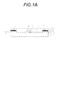
- FIG. 1A and FIG. 1B are cross-sectional views showing a preferred configuration among the capacitance-type input device of the present invention.
- the capacitive input device 10 includes a front plate 1 ′ (cover glass), a white colored layer 2a, a light shielding layer 2b, a first transparent electrode pattern 3, and a second transparent electrode pattern 4. Insulating layer 5, conductive element 6, and transparent protective layer 7.
- the front plate 1 and / or 1 ′ is preferably composed of a translucent substrate.
- the translucent base material uses either the cover glass 1 ′ provided with the following decorating material, or the cover glass 1 ′ followed by the film base material 1 provided with the following decorating material on the film base. I can do it.
- a cover glass 1 ′ can be further provided on the opposite side of the film base electrode.
- tempered glass typified by gorilla glass manufactured by Corning Inc. can be used.
- the side in which each element of the front plate 1 and / or 1 ′ is provided is referred to as a non-contact surface 1a.
- input is performed by bringing a finger or the like into contact with the contact surface of the front plate 1 and / or 1 ′ (the surface opposite to the non-contact surface 1a).
- the front plate may be referred to as a “base material”.
- a white colored layer 2a and a light shielding layer 2b are provided on the non-contact surface of the front plate 1 and / or 1 ′.
- the white colored layer 2a and the light-shielding layer 2b are frame-like patterns around the display area formed on the non-contact side of the touch panel front plate as decorating materials. It is formed for the purpose of decoration.
- the capacitive input device 10 of the present invention can be provided with a wiring outlet (not shown).
- a plurality of first transparent electrode patterns 3 formed with a plurality of pad portions extending in the first direction via connection portions, and the first A plurality of second transparent electrode patterns 4 comprising a plurality of pad portions that are electrically insulated from the transparent electrode pattern 3 and extend in a direction intersecting the first direction, and the first transparent electrode
- An insulating layer 5 that electrically insulates the pattern 3 from the second transparent electrode pattern 4 is formed.
- the first transparent electrode pattern 3, the second transparent electrode pattern 4, and the conductive element 6 to be described later are, for example, translucent conductive materials such as ITO (Indium Tin Oxide) and IZO (Indium Zinc Oxide). It can be made of a conductive metal oxide film.
- metal films examples include ITO films; metal films such as Al, Zn, Cu, Fe, Ni, Cr, and Mo; metal oxide films such as SiO 2 .
- the film thickness of each element can be set to 10 to 200 nm.
- the amorphous ITO film is made into a polycrystalline ITO film by firing, the electrical resistance can be reduced.
- said 1st transparent electrode pattern 3, the 2nd transparent electrode pattern 4, and the electroconductive element 6 mentioned later are manufactured using the transfer film which has the decorating material using the said electroconductive fiber. You can also.
- paragraphs [0014] to [0016] of Japanese Patent No. 4506785 can be referred to.
- the first transparent electrode pattern 3 and the second transparent electrode pattern 4 is opposite to the non-contact surface of the front plate 1 and / or 1 ′ and the front plate 1 and / or 1 ′ of the light shielding layer 2b. Can be installed across both areas of the side surface.
- the second transparent electrode pattern 4 has both the non-contact surface of the front plate 1 and / or 1 ′ and the surface opposite to the front plate 1 and / or 1 ′ of the light shielding layer 2b.
- the figure shows that the second transparent electrode pattern 4 covers the side surface of the white colored layer 2a.
- the width of the white colored layer 2a can be narrower than the width of the light shielding layer 2b.
- At least one of the first transparent electrode pattern 3 and the second transparent electrode pattern 4 is a front plate. 1 and / or 1 'non-contact surface, and the white colored layer 2a and the light shielding layer 2b can be installed across the region of the surface opposite to the front plate 1 and / or 1'.
- the film transfer material particularly the thermoplastic resin layer
- a conductive element 6 is provided on the surface of the light shielding layer 2b opposite to the front plate 1 and / or 1 '.
- the conductive element 6 is electrically connected to at least one of the first transparent electrode pattern 3 and the second transparent electrode pattern 4, and is different from the first transparent electrode pattern 3 and the second transparent electrode pattern 4. Is another element.
- FIG. 1A and FIG. 1B the figure by which the electroconductive element 6 is connected to the 2nd transparent electrode pattern 4 is shown.
- the transparent protective layer 7 is installed so that all of each component may be covered.
- the transparent protective layer 7 may be configured to cover only a part of each component.
- the insulating layer 5 and the transparent protective layer 7 may be made of the same material or different materials.
- the material constituting the insulating layer 5 and the transparent protective layer 7 is preferably a material having high surface hardness and high heat resistance, and a known photosensitive siloxane resin material, acrylic resin material, or the like is used.
- the capacitance type input device and the image display device including the capacitance type input device as a component are “latest touch panel technology” (Techno Times, issued on July 6, 2009), supervised by Yuji Mitani.
- the configurations disclosed in “Technology and Development of Touch Panels”, CMC Publishing (2004, 12), FPD International 2009 Forum T-11 Lecture Textbook, Cypress Semiconductor Corporation Application Note AN2292, etc. can be applied.
- the information display device of the present invention has the touch panel of the present invention.
- the information display device that can use the touch panel of the present invention is preferably a mobile device, and examples thereof include the following information display devices.
- iPhone4, iPad above made by Apple Inc., USA
- Xperia SO-01B
- Galaxy S SC-02B
- Galaxy Tab SC-01C
- BlackBerry 8707h manufactured by Kankoku Research in Motion
- Kindle manufactured by Amazon, USA
- Kobo Touch manufactured by Rakuten, Inc.
- Black dispersion 1 (GB4016, manufactured by Sanyo Pigment Co., Ltd., the following composition) Black pigment (carbon black) 25.0 mass% Dispersing aid 9.5% by mass Dispersing solvent (propylene glycol monomethyl ether acetate) 65.5% by mass
- Black dispersion 2 (CDP-K106, manufactured by FUJIFILM Electromaterials Co., Ltd., the following composition) Black pigment (titanium dioxide) 25.0% by mass Dispersing aid 7.0% by mass Dispersion solvent (methyl ethyl ketone) 68.0% by mass
- White dispersion (FP White B422, manufactured by Sanyo Dye Co., Ltd., the following composition)
- White pigment titanium dioxide
- Dispersing aid 3.5% by mass
- Dispersing solvent methyl ethyl ketone
- Antioxidant (IRGAFOS 168, manufactured by BASF, the following compound)
- Acrylic resin solution (the following composition) Benzyl methacrylate / methacrylic acid random copolymer (molar ratio 78/22, weight average molecular weight 38,000) 27% by mass Propylene glycol monomethyl ether acetate 73% by mass
- Organic solvent 1 (propylene glycol monomethyl ether acetate)
- Organic solvent 2 (methyl ethyl ketone)
- Organic solvent 3 (cyclohexanone)
- a coating solution for a thermoplastic resin layer having the following formulation H1 was applied and dried using a slit nozzle.
- an intermediate layer coating solution having the following formulation P1 was applied and dried.
- the black colored liquids 1 to 4 and the white colored liquids 1 to 2 in Table 1 are further coated and dried, respectively. And a white colored layer was formed.
- a protective film thickness 12 ⁇ m polypropylene film
- the white transfer materials 1 and 2 and the black transfer materials 1 to 4 shown in Table 2 below in which the temporary support, the thermoplastic resin layer, the intermediate layer (oxygen barrier film), the light shielding layer, and the white colored layer are integrated, are obtained.
- Produced. The film thickness and optical density of the white colored layer and the light shielding layer of each transfer material were measured. The results are shown in Table 2 below.
- the film thickness was measured using P-10 manufactured by Tencor Instruments.
- the optical density was measured using BMT-1 manufactured by Sakata Inx Corporation.
- the white transfer material 1 of Production Example 1 was formed into a frame shape having a size corresponding to the four sides of the glass substrate, and then transferred. Details are shown below. First, the white transfer material 1 of Production Example 1 was cut into a frame shape so as to have a size corresponding to the four sides of the glass substrate. Next, the protective film was peeled from the white transfer material 1 after cutting. Thereafter, the surface of the white colored layer exposed by peeling off the protective film is superposed so that the surface of the glass substrate preheated at 50 ° C. is in contact with a laminator (manufactured by Hitachi Industries, Ltd. (Lamic II type).
- a laminator manufactured by Hitachi Industries, Ltd. (Lamic II type).
- the glass substrate (base material) was heated at 150 ° C. for 30 minutes.
- the black transfer material 1 of Production Example 2 was transferred onto the cured white colored layer, and the temporary support, the thermoplastic resin layer, and the intermediate layer were removed in the same manner as the white transfer material 1. Then, assuming ITO sputtering, heating was performed at 280 ° C. for 30 minutes to obtain a base material with a decorating material of Example 1 in which a glass substrate, a white colored layer, and a light shielding layer were laminated in this order.
- Example 1 a white colored layer and a light-shielding layer were formed on a glass substrate in the same manner as in Example 1 except that the white transfer material and the black transfer material used were changed as shown in Table 3 below.
- the base material with a decorating material of 2, 3 and Comparative Example 1 was obtained.
- optical density The optical density of the base material with a decorating material of each Example and Comparative Example prepared above was measured using BMT-1 manufactured by Sakata Inx Corporation.
- Example 101 Production of touch panel] ⁇ Formation of first transparent electrode pattern> ⁇ Formation of transparent electrode layer>
- etching transfer film E1 Preparation of the white transfer material 1 of Preparation Example 1 except that the white colored liquid 1 was replaced with a coating liquid for photocurable resin layer for etching having the following formulation E1.
- an etching transfer film E1 in which the temporary support, the thermoplastic resin layer, the intermediate layer (oxygen barrier film), the photocurable resin layer for etching and the protective film were integrated was obtained (for etching)
- the film thickness of the photocurable resin layer was 2.0 ⁇ m).
- the distance between the exposure mask (quartz exposure mask having a transparent electrode pattern) surface and the photocurable resin layer for etching is set to 200 ⁇ m, and the exposure amount is 50 mJ / cm 2 (i-line). )
- the exposure amount is 50 mJ / cm 2 (i-line).
- T-PD2 triethanolamine developer
- pure water 25 ° C. for 100 times. Processed for seconds.
- the residue was removed by treating at 33 ° C. for 20 seconds, Furthermore, the post-baking process for 30 minutes was performed at 130 degreeC, and the front board in which the white colored layer, the light shielding layer, the transparent electrode layer, and the photocurable resin layer pattern for an etching were formed was obtained.
- a surfactant-containing cleaning solution trade name: T-SD3 (manufactured by FUJIFILM Corporation) diluted 10-fold with pure water
- the front plate on which the white colored layer, the light-shielding layer, the transparent electrode layer and the photocurable resin layer pattern for etching are formed is immersed in an etching bath containing ITO etchant (hydrochloric acid, potassium chloride aqueous solution, liquid temperature 30 ° C.) Transparent electrode layer treated for 100 seconds to dissolve and remove the exposed transparent electrode layer not covered with the photocurable resin layer for etching, with a white colored layer, a light shielding layer, and a photocurable resin layer pattern for etching A front plate with a pattern was obtained.
- ITO etchant hydroochloric acid, potassium chloride aqueous solution, liquid temperature 30 ° C.
- a front plate with a transparent electrode layer pattern with a photocurable resin layer pattern for etching is applied to a resist stripping solution (N-methyl-2-pyrrolidone, monoethanolamine, a surfactant (trade name: Surfynol 465). Manufactured by Air Products) in a resist stripping tank containing a liquid temperature of 45 ° C. and treated for 200 seconds to remove the photo-curable resin layer for etching, a white colored layer, a light-shielding layer, and a front plate
- a front plate having a first transparent electrode pattern installed as shown in FIG. 1A across both the contact surface and the region opposite to the front plate side of the light shielding layer was obtained.
- ⁇ Formation of insulating layer> ⁇ Preparation of transfer film W1 for forming an insulating layer>
- the white colored liquid 1 is replaced with a coating liquid for forming an insulating layer having the following formulation W1.
- a temporary support, a thermoplastic resin layer, an intermediate layer (oxygen barrier film), a photocurable resin layer for insulating layer, and a protective film were integrated to obtain an insulating layer forming transfer film W1 (light for insulating layer).
- the film thickness of the curable resin layer is 1.4 ⁇ m).
- DPHA dipentaerythritol hexaacrylate
- Propylene glycol monomethyl ether acetate solution (76% by mass) : 1.4 parts by mass / urethane-based monomer (trade name: NK Oligo UA-32P, manufactured by Shin-Nakamura Chemical Co., Ltd .: non-volatile content 75%, propylene glycol monomethyl ether acetate: 25%): 0.68 parts by mass.
- Tripentaerythritol octaacrylate (trade name: V # 802, Osaka Organic Chemical Industry Co., Ltd.): 1.8 parts by mass.
- the white colored layer, the light shielding layer, and the front plate with the first transparent electrode pattern were washed with a rotating brush having nylon hair while spraying a glass detergent solution adjusted to 25 ° C. for 20 seconds by a shower.
- a transfer film W1 for forming an insulating layer from which the protective film was removed was laminated on the washed front plate (base material temperature: 100 ° C., rubber roller temperature 120 ° C., linear pressure 100 N / cm, conveyance speed 2.3 m / second). Min).
- the distance between the exposure mask (quartz exposure mask having the insulating layer pattern) surface and the photocurable resin layer for forming the insulating layer is set to 100 ⁇ m, and the exposure dose is 30 mJ / cm 2. Pattern exposure was performed with (i-line).
- a triethanolamine developer (containing 30% by mass of triethanolamine, trade name: T-PD2 (manufactured by FUJIFILM Corporation) diluted 10 times with pure water) was used at 33 ° C. for 60 ° C.
- T-PD2 sodium carbonate / sodium hydrogen carbonate developer
- T-CD1 sodium carbonate / sodium hydrogen carbonate developer
- T-SD3 surfactant-containing cleaning solution
- the post-baking process for 60 minutes was performed at 230 degreeC, and the front board in which the white colored layer, the light shielding layer, the 1st transparent electrode pattern, and the insulating layer pattern were formed was obtained.
- the front plate on which the white colored layer, the light shielding layer, the first transparent electrode pattern, and the insulating layer pattern were formed was subjected to DC magnetron sputtering treatment (condition: substrate temperature 50 Before forming an ITO thin film having a thickness of 80 nm and a white colored layer, a light-shielding layer, a first transparent electrode pattern, an insulating layer pattern, and a transparent electrode layer. A face plate was obtained. The surface resistance of the ITO thin film was 110 ⁇ / ⁇ .
- a white colored layer, a light shielding layer, a first transparent electrode pattern, an insulating layer pattern, a transparent electrode layer, a photocurable resin for etching Similar to the formation of the first transparent electrode pattern, using the etching transfer film E1, a white colored layer, a light shielding layer, a first transparent electrode pattern, an insulating layer pattern, a transparent electrode layer, a photocurable resin for etching. A front plate on which a layer pattern was formed was obtained (post-bake treatment; 130 ° C., 30 minutes). Further, in the same manner as the formation of the first transparent electrode pattern, etching (30 ° C., 50 seconds) is performed, and the photo-curable resin layer for etching is removed (45 ° C., 200 seconds), whereby a white colored layer, As shown in FIG.
- the light shielding layer, the first transparent electrode pattern, the insulating layer pattern, the non-contact surface of the front plate, and the surface of the light shielding layer opposite to the front plate side are disposed.
- a front plate on which a second transparent electrode pattern was formed was obtained.
- the front plate on which the white colored layer, the light-shielding layer, the first transparent electrode pattern, the insulating layer pattern, and the second transparent electrode pattern are formed is a DC magnetron.
- a front plate on which an aluminum (Al) thin film having a thickness of 200 nm was formed was obtained by sputtering.
- a white colored layer, a light shielding layer, a first transparent electrode pattern, an insulating layer pattern, and a second transparent electrode are formed using the etching transfer film E1.
- a front plate on which a pattern, an aluminum thin film, and a photocurable resin layer pattern for etching were formed was obtained (post-baking treatment; 130 ° C., 30 minutes).
- etching (30 ° C., 50 seconds) is performed, and the photo-curable resin layer for etching is removed (45 ° C., 200 seconds), whereby a white colored layer, A front plate having a light shielding layer, a first transparent electrode pattern, an insulating layer pattern, a second transparent electrode pattern, and a conductive element (aluminum thin film) different from the first and second transparent electrode patterns was obtained.
- the transfer film W1 for forming the insulating layer from which the protective film has been removed is laminated on the front plate formed up to the conductive element different from the first and second transparent electrode patterns, After peeling off the support, front exposure is performed at an exposure amount of 50 mJ / cm 2 (i-line) without using an exposure mask, development, post-exposure (1000 mJ / cm 2 ), and post-baking treatment are performed to obtain a white colored layer, light shielding Layer, first transparent electrode pattern, insulating layer pattern, second transparent electrode pattern, insulating layer (transparent protective layer) so as to cover all of the conductive elements different from the first and second transparent electrode patterns A front plate 1 laminated as shown in FIG. 1A was obtained. The obtained front plate 1 was used as the capacitive input device of Example 1.
- the transparent protective layer was free from defects such as bubbles and an image display device having excellent display characteristics was obtained.
- the black colored liquid described in Table 4 below was applied to the temporary support, the thermoplastic resin layer, and the intermediate layer prepared in Examples 1 to 3 in the same manner as when the black colored liquid was applied and dried in Examples 1 to 3. 5 to 9 were applied and dried so that the OD was 4.5. Further, each of the white colored liquids 1 listed in Table 1 was applied and dried so that the film thickness after drying was 35 ⁇ m, and the white color layer / light-shielding layer laminated transfer materials 1 to 5 shown in Table 5 below were applied. Obtained.
- the white colored layer / light-shielding layer laminated transfer materials 1 to 5 were transferred onto a glass substrate and heated at 280 ° C. for 30 minutes assuming ITO sputtering.
- the base material with a decorating material was obtained.
- Example 106 A front plate of Example 106 was obtained in the same manner as in Example 101 except that the base material with a decorative material of Example 6 was used instead of the base material with a decorative material of Example 1. This front plate was preferable like the front plates of the other examples.
- Example 201, comparative example 201 (Thermal transfer printing method) A white colored liquid 1 and 2 and a black colored liquid 1 and 4 on a surface opposite to the heat resistant slipping layer of a PET film having a thickness of 15 ⁇ m having a heat resistant slipping layer on one side and a dry film thickness of 9.0 ⁇ m, respectively. , 9.0 ⁇ m, 1.6 ⁇ m, and 2.0 ⁇ m, and dried to obtain thermal transfer ribbons White 1 and White 2, Black 1 and Black 4.
- the white colored layer derived from the white colored liquid 1 was transferred onto the glass substrate by pressing the thermal transfer ribbon white 1. This was repeated 4 times to obtain a white colored layer 1 having a thickness of 36 ⁇ m. This was heated at 150 ° C. for 30 minutes to be hardened. On this white colored layer 1, the thermal transfer ribbon black 1 was pressed and the light shielding layer derived from the black colored liquid 1 was transferred, and the base material with a decorating material of Example 201 was obtained.
- the thermal coloring ribbon white 2 was pressed on the glass substrate, and the white colored layer derived from the white colored liquid 2 was transcribe
- Example 1 As in Example 1, assuming ITO sputtering, the substrates with the decorating material of Example 201 and Comparative Example 201 were heated at 280 ° C. for 30 minutes in a nitrogen atmosphere, and b as the color after the high-temperature treatment. The value was measured.
- the b value of the base material with a decorating material of Example 201 is 3.2
- the b value of the base material with a decorating material of Comparative Example 201 is 12, and (A1) is not significantly colored after the high temperature treatment. I understood.
- Example 301, comparative example 301 (Inkjet printing method)
- the white coloring liquid 1 was inkjet-printed on the glass substrate using the inkjet head of discharge amount 1.8pL, and printed matter was dried at 150 degreeC for 30 minutes. This operation was further repeated 5 times to produce a white colored layer 1b having a thickness of 36 ⁇ m.
- the black colored liquid 1 is printed on the white colored layer 1b in the same manner as the white colored layer 1b, and then dried at 150 ° C. for 30 minutes to form a light-shielding layer 1b having a thickness of 2.0 ⁇ m.
- the base material with a decorating material of Example 301 was obtained.
- the amount of ink discharged was adjusted, white coloring liquid 2 and black coloring liquid 4 were used, and a white colored layer 2b having a thickness of 36 ⁇ m and a light shielding layer 4b having a thickness of 2.0 ⁇ m were formed on a glass substrate.
- a base material with a decorative material was obtained.
- Example 1 As in Example 1, assuming ITO sputtering, the substrates with the decorating material of Example 301 and Comparative Example 301 were heated at 280 ° C. for 30 minutes in a nitrogen atmosphere, and b as the color after the high-temperature treatment. The value was measured.
- the b value of the base material with a decorating material of Example 301 is 3.2
- the b value of the base material with a decorating material of Comparative Example 301 is 12
- the base material with the decorating material of Example 301 is subjected to high temperature treatment. It was found that it was not significantly colored.
- Example 401, comparative example 401 (Screen printing method)
- the white colored liquids 1 and 2 were adjusted to 1000 mPa ⁇ s by reducing the ratio of each of the organic solvents 1 to 3, and white colored liquids 1a and 2a were prepared.
- the black colored liquids 1 and 4 were adjusted to 200 mPa ⁇ s by reducing the ratio of each of the organic solvents 1 to 3, thereby preparing black colored liquids 1a and 4a.
- a white colored layer 1a having a thickness of 18 ⁇ m was produced from the white colored liquid 1a on a glass substrate using a polyester screen having a 225 mesh (opening diameter, 65 ⁇ m) and a thickness of 72 ⁇ m. This was repeated to produce a white colored layer 1a having a thickness of 36 ⁇ m. This was heated at 150 ° C. for 30 minutes to be hardened. On this white colored layer 1a, a black colored liquid 1a was used to laminate a 1.6 mm thick light-shielding layer 1a to obtain a base material with a decorating material of Example 401.
- a white colored liquid 2a is used instead of the white colored liquid 1a to produce a 36.0 ⁇ m white colored layer 2a, and a black colored liquid 4a is used instead of the black colored liquid 1a to form a 1.6 ⁇ m thick light shielding layer 1a.
- a base material with a decorating material of Comparative Example 401 was obtained by laminating a light shielding layer 4 a having a thickness of 2.0 ⁇ m instead of.
- Example 1 As in Example 1, assuming ITO sputtering, the substrates with decorating materials of Example 401 and Comparative Example 401 were heated at 280 ° C. for 30 minutes in a nitrogen atmosphere, and b as the color after high-temperature treatment. The value was measured.
- the b value of the base material with a decorating material of Example 401 is 3.2, the b value of the base material with a decorating material of Comparative Example 401 is 12, and the base material with the decorating material of Example 401 is subjected to high temperature treatment. It was found that it was not significantly colored.
- Substrate film substrate. Only the film substrate may be used as the front plate
- 1 'glass cover glass. Only the cover glass may be used as a front plate, and a laminate of a substrate and glass may be used as a front plate
- 2a White colored layer 2b
- Light-shielding layer 3
- Conductive layer (first transparent electrode pattern) 4
- Conductive layer (second electrode pattern) 5
- Insulating layer 6
- Transparent protective layer 10 Capacitive input device
Landscapes
- Engineering & Computer Science (AREA)
- General Engineering & Computer Science (AREA)
- Theoretical Computer Science (AREA)
- Human Computer Interaction (AREA)
- Physics & Mathematics (AREA)
- General Physics & Mathematics (AREA)
- Laminated Bodies (AREA)
- Liquid Crystal (AREA)
- Position Input By Displaying (AREA)
Abstract
本発明は、白色着色層および遮光層を有し、高温処理後の白色着色層のb値が小さい加飾材付き基材を提供する。本発明の加飾材付き基材は、基材、白色着色層および遮光層をこの順で含み、前記白色着色層と前記遮光層がいずれもシロキサン結合を主鎖に有する樹脂を含む。
Description
本発明は、加飾材付き基材およびその製造方法、該加飾材付き基材を備えたタッチパネルならびに該タッチパネルを備えた情報表示装置に関する。
携帯電話、カーナビゲーション、パーソナルコンピュータ、券売機、銀行の端末などの電子機器では、近年、液晶装置などの表面にタッチパネル型の入力装置が配置され、液晶装置の画像表示領域に表示された指示画像を参照しながら、この指示画像が表示されている箇所に指またはタッチペンなどを触れることで、指示画像に対応する情報の入力が行えるものがある。
このような入力装置(タッチパネル)には、抵抗膜型、静電容量型などがある。静電容量型の入力装置は、単に一枚の基板に透光性導電膜を形成すればよいという利点がある。
このような入力装置(タッチパネル)には、抵抗膜型、静電容量型などがある。静電容量型の入力装置は、単に一枚の基板に透光性導電膜を形成すればよいという利点がある。
このような静電容量型の入力装置においては、表示装置の引き回し回路等を使用者から視認されないようにするため、また見栄えをよくするため、指またはタッチペンなどで触れる情報表示部(画像表示部)を囲む枠状に加飾材が形成されて、加飾が行われている。例えば、特許文献1には、シリコーン成分を含有するインキを用いてスクリーン印刷法によりカバーガラス基板上に加飾部を形成する工程と、カバーガラス基板上の加飾部を研磨する工程と、カバーガラス基板上にオーバーコート層を塗布する工程と、オーバーコート層の上にタッチパネルセンサーを形成する工程と、タッチパネルセンサーごとにカバーガラス基板を断裁する工程と、をこの順で含むことを特徴とする加飾カバーガラス一体型タッチパネルの製造方法が記載されており、黒色のシリコーン含有インクを用いて加飾材を形成した例が記載されている。
一方、白色着色層を加飾材として用いることは、その光学濃度を高めることが難しいという問題があった。
ここで、特許文献1で使用されているような黒色のシリコーン含有樹脂層は、インクジェット印刷用インク組成物中でカーボンブラックの結合剤として用いられた例などが知られているが(例えば特許文献2参照)、シリコーン含有樹脂を白色の加飾材に応用することなどについてはいずれの文献にも開示も示唆もなかった。
このような状況のもと、本発明者らが白色着色層を加飾材として用いることを検討したところ、接触面側に白色着色層を額縁状に設け、さらに白色着色層の裏に光学濃度を高めるために遮光層を設けることで、加飾材の透けを抑制できることがわかった。
しかしながら、静電容量型入力装置を製造するときには、白色着色層および遮光層を形成した後の工程において導電性層(たとえばITO透明電極パターン)を蒸着などにより形成すると、導電性層の形成時に白色着色層および遮光層が加熱されて白色着色層が着色し、b値が大きくなるという従来知られていなかった新たな課題があることが判明した。
本発明が解決しようとする課題は、白色着色層および遮光層を有し、高温処理後の白色着色層のb値が小さい加飾材付き基材を提供することである。
本発明者らは、前記課題を解決するために鋭意研究を重ねた結果、白色着色層と前記遮光層にいずれもシロキサン結合を主鎖に有する樹脂を用いることで、高温処理後の白色着色層のb値を小さくできることを見出した。
すなわち、以下に示す構成の本発明により、前記課題が解決できることを見出し、本発明の完成に至った。
すなわち、以下に示す構成の本発明により、前記課題が解決できることを見出し、本発明の完成に至った。
[1] 基材、白色着色層および遮光層をこの順で含み、前記白色着色層と前記遮光層がいずれもシロキサン結合を主鎖に有する樹脂を含むことを特徴とする加飾材付き基材。
[2] [1]に記載の加飾材付き基材は、前記遮光層上に、さらに導電性層を有することが好ましい。
[3] [2]に記載の加飾材付き基材は、前記導電性層が、インジウムを含むことが好ましい。
[4] [1]~[3]のいずれか一項に記載の加飾材付き基材は、前記遮光層の表面抵抗が、1.0×10¹⁰Ω/□以上であることが好ましい。
[5] [1]~[4]のいずれか一項に記載の加飾材付き基材は、前記白色着色層と前記遮光層がいずれも顔料を含むことが好ましい。
[6] [5]に記載の加飾材付き基材は、前記白色着色層中に含まれる前記顔料以外の全成分に対する前記シロキサン結合を主鎖に有する樹脂の割合が90質量%以上であり、かつ、
前記遮光層中に含まれる前記顔料以外の全成分に対する前記シロキサン結合を主鎖に有する樹脂の割合が70質量%以上であることが好ましい。
[7] [1]~[6]のいずれか一項に記載の加飾材付き基材は、前記白色着色層が、酸化チタンを含むことが好ましい。
[8] [1]~[7]のいずれか一項に記載の加飾材付き基材は、前記白色着色層の膜厚が、10μm~40μmであることが好ましい。
[9] [1]~[8]のいずれか一項に記載の加飾材付き基材は、前記遮光層が、酸化チタンおよびカーボンブラックのうち少なくとも一つを含むことが好ましい。
[10] [1]~[9]のいずれか一項に記載の加飾材付き基材は、前記遮光層の膜厚が、1.0μm~5.0μmであることが好ましい。
[11] [1]~[10]のいずれか一項に記載の加飾材付き基材は、加飾材付き基材の光学濃度が、3.5~6.0であることが好ましい。
[12] [1]~[11]のいずれか一項に記載の加飾材付き基材は、加飾材付き基材の前記基材側の色味が、SCI指標で、L値が85~95、b値が1.5~4.0であることが好ましい。
[13] [1]~[12]のいずれか一項に記載の加飾材付き基材は、前記基材が、ガラス、シクロオレフィンポリマーまたはシリコーン樹脂からなることが好ましい。
[14] [13]に記載の加飾材付き基材は、シリコーン樹脂が籠型ポリオルガノシルセスキオキサンを主成分とすることが好ましい。
[15] 基材上に白色着色層および遮光層をこの順で積層する工程を含み、
前記白色着色層および前記遮光層が、それぞれ下記の方法から選択される方法で作成され、該方法において用いる白色着色層、遮光層、白色着色層形成用組成物および遮光層形成用組成物が、いずれもシロキサン結合を主鎖に有する樹脂を含むことを特徴とする加飾材付き基材の製造方法。
仮支持体上に少なくとも白色着色層および遮光層の一方を含むフィルム転写材料から少なくとも該白色着色層および該遮光層の一方を転写した後に該仮支持体を取り除く方法
仮支持体上に少なくとも白色着色層および遮光層の一方を含む熱転写材料の該仮支持体側を加熱して、該仮支持体から少なくとも該白色着色層および該遮光層の一方を転写する熱転写印刷
白色着色層形成用の組成物または遮光層形成用の組成物のスクリーン印刷、および、
白色着色層形成用組成物または遮光層形成用組成物のインクジェット印刷
[16] [15]に記載の加飾材付き基材の製造方法は、前記白色着色層および前記遮光層を、
少なくとも仮支持体、遮光層および白色着色層の順に含むフィルム転写材料から該遮光層および該白色着色層を、前記基材上に転写した後に該仮支持体を取り除くこと、あるいは、
仮支持体および白色着色層を有するフィルム転写材料から該白色着色層を基材上に転写した後に該仮支持体を取り除き、さらに少なくとも仮支持体および遮光層を含むフィルム転写材料から該遮光層を前記白色着色層上に転写した後に該仮支持体を取り除くこと、により形成することが好ましい。
[17] [1]~[14]のいずれか一項に記載の加飾材付き基材を含むことを特徴とするタッチパネル。
[18] [17]に記載のタッチパネルを有することを特徴とする情報表示装置。
[2] [1]に記載の加飾材付き基材は、前記遮光層上に、さらに導電性層を有することが好ましい。
[3] [2]に記載の加飾材付き基材は、前記導電性層が、インジウムを含むことが好ましい。
[4] [1]~[3]のいずれか一項に記載の加飾材付き基材は、前記遮光層の表面抵抗が、1.0×10¹⁰Ω/□以上であることが好ましい。
[5] [1]~[4]のいずれか一項に記載の加飾材付き基材は、前記白色着色層と前記遮光層がいずれも顔料を含むことが好ましい。
[6] [5]に記載の加飾材付き基材は、前記白色着色層中に含まれる前記顔料以外の全成分に対する前記シロキサン結合を主鎖に有する樹脂の割合が90質量%以上であり、かつ、
前記遮光層中に含まれる前記顔料以外の全成分に対する前記シロキサン結合を主鎖に有する樹脂の割合が70質量%以上であることが好ましい。
[7] [1]~[6]のいずれか一項に記載の加飾材付き基材は、前記白色着色層が、酸化チタンを含むことが好ましい。
[8] [1]~[7]のいずれか一項に記載の加飾材付き基材は、前記白色着色層の膜厚が、10μm~40μmであることが好ましい。
[9] [1]~[8]のいずれか一項に記載の加飾材付き基材は、前記遮光層が、酸化チタンおよびカーボンブラックのうち少なくとも一つを含むことが好ましい。
[10] [1]~[9]のいずれか一項に記載の加飾材付き基材は、前記遮光層の膜厚が、1.0μm~5.0μmであることが好ましい。
[11] [1]~[10]のいずれか一項に記載の加飾材付き基材は、加飾材付き基材の光学濃度が、3.5~6.0であることが好ましい。
[12] [1]~[11]のいずれか一項に記載の加飾材付き基材は、加飾材付き基材の前記基材側の色味が、SCI指標で、L値が85~95、b値が1.5~4.0であることが好ましい。
[13] [1]~[12]のいずれか一項に記載の加飾材付き基材は、前記基材が、ガラス、シクロオレフィンポリマーまたはシリコーン樹脂からなることが好ましい。
[14] [13]に記載の加飾材付き基材は、シリコーン樹脂が籠型ポリオルガノシルセスキオキサンを主成分とすることが好ましい。
[15] 基材上に白色着色層および遮光層をこの順で積層する工程を含み、
前記白色着色層および前記遮光層が、それぞれ下記の方法から選択される方法で作成され、該方法において用いる白色着色層、遮光層、白色着色層形成用組成物および遮光層形成用組成物が、いずれもシロキサン結合を主鎖に有する樹脂を含むことを特徴とする加飾材付き基材の製造方法。
仮支持体上に少なくとも白色着色層および遮光層の一方を含むフィルム転写材料から少なくとも該白色着色層および該遮光層の一方を転写した後に該仮支持体を取り除く方法
仮支持体上に少なくとも白色着色層および遮光層の一方を含む熱転写材料の該仮支持体側を加熱して、該仮支持体から少なくとも該白色着色層および該遮光層の一方を転写する熱転写印刷
白色着色層形成用の組成物または遮光層形成用の組成物のスクリーン印刷、および、
白色着色層形成用組成物または遮光層形成用組成物のインクジェット印刷
[16] [15]に記載の加飾材付き基材の製造方法は、前記白色着色層および前記遮光層を、
少なくとも仮支持体、遮光層および白色着色層の順に含むフィルム転写材料から該遮光層および該白色着色層を、前記基材上に転写した後に該仮支持体を取り除くこと、あるいは、
仮支持体および白色着色層を有するフィルム転写材料から該白色着色層を基材上に転写した後に該仮支持体を取り除き、さらに少なくとも仮支持体および遮光層を含むフィルム転写材料から該遮光層を前記白色着色層上に転写した後に該仮支持体を取り除くこと、により形成することが好ましい。
[17] [1]~[14]のいずれか一項に記載の加飾材付き基材を含むことを特徴とするタッチパネル。
[18] [17]に記載のタッチパネルを有することを特徴とする情報表示装置。
本発明によれば、白色着色層および遮光層を有し、高温処理後の白色着色層のb値が小さい加飾材付き基材を提供することができる。
以下、本発明の加飾材付き基材、タッチパネルおよび情報表示装置について詳細に説明する。
以下に記載する構成要件の説明は、本発明の代表的な実施態様に基づいてなされることがあるが、本発明はそのような実施態様に限定されるものではない。なお、本明細書において「~」を用いて表される数値範囲は、「~」の前後に記載される数値を下限値および上限値として含む範囲を意味する。
以下に記載する構成要件の説明は、本発明の代表的な実施態様に基づいてなされることがあるが、本発明はそのような実施態様に限定されるものではない。なお、本明細書において「~」を用いて表される数値範囲は、「~」の前後に記載される数値を下限値および上限値として含む範囲を意味する。
[加飾材付き基材]
本発明の加飾材付き基材は、基材、白色着色層および遮光層をこの順で含み、前記白色着色層と前記遮光層がいずれもシロキサン結合を主鎖に有する樹脂を含むことを特徴とする。
このような構成により、本発明の加飾材付き基材は、白色着色層および遮光層を有し、高温処理後の白色着色層のb値が小さい。いかなる理論に拘泥するものでもないが、シロキサン結合を主鎖に有する樹脂を用いた白色着色層および遮光層は、高温処理後(例えば280℃で30分間の処理)でも、シロキサン結合を主鎖に有する樹脂は分解などが生じ難く、b値が小さい。特に、白色着色層自体にのみシロキサン結合を主鎖に有する樹脂を含む場合よりも、白色着色層および遮光層がいずれもシロキサン結合を主鎖に有する樹脂を含む場合の方が、高温処理後のb値を小さくすることができる。
以下、本発明の加飾材付き基材の好ましい態様について説明する。
本発明の加飾材付き基材は、基材、白色着色層および遮光層をこの順で含み、前記白色着色層と前記遮光層がいずれもシロキサン結合を主鎖に有する樹脂を含むことを特徴とする。
このような構成により、本発明の加飾材付き基材は、白色着色層および遮光層を有し、高温処理後の白色着色層のb値が小さい。いかなる理論に拘泥するものでもないが、シロキサン結合を主鎖に有する樹脂を用いた白色着色層および遮光層は、高温処理後(例えば280℃で30分間の処理)でも、シロキサン結合を主鎖に有する樹脂は分解などが生じ難く、b値が小さい。特に、白色着色層自体にのみシロキサン結合を主鎖に有する樹脂を含む場合よりも、白色着色層および遮光層がいずれもシロキサン結合を主鎖に有する樹脂を含む場合の方が、高温処理後のb値を小さくすることができる。
以下、本発明の加飾材付き基材の好ましい態様について説明する。
<加飾材付き基材の特性>
本発明の加飾材付き基材における「加飾材」とは、前記白色着色層と前記遮光層の積層体のことを意味する。白色着色層のみを基材に転写して加飾材とする場合、光学濃度が低く、本発明の製造方法で得られる加飾材付き基材を表示装置の基材として用いたときには表示装置の光漏れが起きたり、回路がすけて見える場合がある。本発明の加飾材付き基材では、基材(フィルムまたはガラス)側より白色着色層および遮光層をこの順で含む構成とすることで光漏れ等を抑えることが出来る。
本発明の加飾材付き基材における「加飾材」とは、前記白色着色層と前記遮光層の積層体のことを意味する。白色着色層のみを基材に転写して加飾材とする場合、光学濃度が低く、本発明の製造方法で得られる加飾材付き基材を表示装置の基材として用いたときには表示装置の光漏れが起きたり、回路がすけて見える場合がある。本発明の加飾材付き基材では、基材(フィルムまたはガラス)側より白色着色層および遮光層をこの順で含む構成とすることで光漏れ等を抑えることが出来る。
本発明の加飾材付き基材は、加飾材付き基材の光学濃度が、3.5~6.0であることが好ましく、4.0~5.5であることがより好ましく、4.5~5.0であることが特に好ましい。
本発明の加飾材付き基材は、加飾材付き基材の前記基材側の色味が、SCI指標で、L値が85~95であることが好ましく、86~95であることがより好ましく、87~95であることが特に好ましく、88~95であることがより特に好ましい。さらに本発明の加飾材付き基材は、280℃、30分間の高温処理後の加飾材付き基材の前記基材側のL値がSCI指標で、上記範囲であることが、前記遮光層の上に導電性層をスパッタにより蒸着した後の色味を改善する観点から好ましい。
本発明の加飾材付き基材は、加飾材付き材料の前記基材側の色味が、SCI指標で、b値が1.5~4.0であることが好ましく、1.5~3.8であることがより好ましく、1.5~3.6であることが特に好ましく、1.5~3.4であることがより特に好ましい。さらに本発明の加飾材付き基材は、280℃、30分間の高温処理後の加飾材付き材料の前記基材側のL値がSCI指標で、上記範囲であることが、前記遮光層の上に導電性層をスパッタにより蒸着した後の色味を改善する観点から好ましい。
<基材>
本発明の加飾材付き基材に用いる基材には、種々のものを用いることが出来るが、前記基材はフィルム基材であることが好ましく、光学的に歪みがないものや、透明度が高いものを用いることがより好ましい。本発明の加飾材付き基材では、前記基材は、全光透過率が、80%以上であることが好ましい。
本発明の加飾材付き基材に用いる基材には、種々のものを用いることが出来るが、前記基材はフィルム基材であることが好ましく、光学的に歪みがないものや、透明度が高いものを用いることがより好ましい。本発明の加飾材付き基材では、前記基材は、全光透過率が、80%以上であることが好ましい。
前記基材がフィルム基材である場合の具体的な素材には、ポリエチレンテレフタレート(PET)、ポリエチレンナフタレート、ポリカーボネート(PC)、トリアセチルセルロース(TAC)、シクロオレフィンポリマー(COP)をあげることができる。
前記基材は、ガラスなどでもよい。
本発明の加飾材付き基材では、前記基材は、ガラス、TAC、PET、PC、COPまたはシリコーン樹脂(ただし、本明細書中におけるシリコーン樹脂やポリオルガノシロキサンは、R2SiOの構造単位式で現れる狭義の意味に限定されるものではなく、RSiO1.5の構造単位式で表されるシルセスキオキサン化合物も含む)から選ばれることが好ましく、ガラス、シクロオレフィンポリマーまたはシリコーン樹脂からなることが好ましい。
シリコーン樹脂は籠型ポリオルガノシロキサンを主成分とすることが好ましく、かご型シルセスキオキサンを主成分とすることがより好ましい。なお、組成物または層の主成分とは、その組成物またはその層の50質量%以上を占める成分のことを言う。前記シリコーン樹脂やシリコーン樹脂を含む基材としては、特許第4142385号、特許第4409397号、特許第5078269号、特許第4920513号、特許第4964748号、特許第5036060号、特開2010-96848号、特開2011-194647号、特開2012-183818号、特開2012-184371号、特開2012-218322号の各公報に記載のものを用いることができ、これらの公報に記載の内容は本発明に組み込まれる。
前記基材は、ガラスなどでもよい。
本発明の加飾材付き基材では、前記基材は、ガラス、TAC、PET、PC、COPまたはシリコーン樹脂(ただし、本明細書中におけるシリコーン樹脂やポリオルガノシロキサンは、R2SiOの構造単位式で現れる狭義の意味に限定されるものではなく、RSiO1.5の構造単位式で表されるシルセスキオキサン化合物も含む)から選ばれることが好ましく、ガラス、シクロオレフィンポリマーまたはシリコーン樹脂からなることが好ましい。
シリコーン樹脂は籠型ポリオルガノシロキサンを主成分とすることが好ましく、かご型シルセスキオキサンを主成分とすることがより好ましい。なお、組成物または層の主成分とは、その組成物またはその層の50質量%以上を占める成分のことを言う。前記シリコーン樹脂やシリコーン樹脂を含む基材としては、特許第4142385号、特許第4409397号、特許第5078269号、特許第4920513号、特許第4964748号、特許第5036060号、特開2010-96848号、特開2011-194647号、特開2012-183818号、特開2012-184371号、特開2012-218322号の各公報に記載のものを用いることができ、これらの公報に記載の内容は本発明に組み込まれる。
また、基材表面には、種々の機能を付加しても良い。具体的には、反射防止層、防眩層、位相差層、視野角向上層、耐傷層、自己修復層、帯電防止層、防汚層、防電磁波層、導電性層をあげることができる。
本発明の加飾材付き基材では、前記基材は、基材表面に導電性層を有することが好ましい。前記導電性層としては、特表2009-505358号公報に記載のものを好ましく用いることができる。
前記基材は、さらに少なくとも、耐傷層および防眩層のうち少なくとも一つを有することが好ましい。
本発明の加飾材付き基材では、前記基材は、基材表面に導電性層を有することが好ましい。前記導電性層としては、特表2009-505358号公報に記載のものを好ましく用いることができる。
前記基材は、さらに少なくとも、耐傷層および防眩層のうち少なくとも一つを有することが好ましい。
本発明の加飾材付き基材では、前記基材は、膜厚が40~200μmであることが好ましく、40~150μmであることがより好ましく、50~120μmであることが特に好ましい。
また、転写工程におけるラミネートによる着色層の密着性を高めるために、予め基材(前面板)の非接触面に表面処理を施すことができる。前記表面処理としては、シラン化合物を用いた表面処理(シランカップリング処理)を実施することが好ましい。シランカップリング剤としては、感光性樹脂と相互作用する官能基を有するものが好ましい。例えばシランカップリング液(N-β(アミノエチル)γ-アミノプロピルトリメトキシシラン0.3質量%水溶液、商品名:KBM603、信越化学(株)製)をシャワーにより20秒間吹き付け、純水シャワー洗浄する。この後、加熱により反応させる。加熱槽を用いてもよく、ラミネーターの基材予備加熱でも反応を促進できる。
<白色着色層>
本発明の加飾材付き基材は、前記基材と前記遮光層の間に白色着色層を含み、前記白色着色層はシロキサン結合を主鎖に有する樹脂を含む。前記白色着色層は顔料を含むことが好ましい。
本発明の加飾材付き基材は、前記基材と前記遮光層の間に白色着色層を含み、前記白色着色層はシロキサン結合を主鎖に有する樹脂を含む。前記白色着色層は顔料を含むことが好ましい。
(シロキサン結合を主鎖に有する樹脂)
前記白色着色層はシロキサン結合を主鎖に有する樹脂を含む。但し、本発明の加飾材付き基材は、本発明の趣旨に反しない限りにおいて前記白色着色層中に前記顔料以外の成分を含んでいてもよい。
前記白色着色層はシロキサン結合を主鎖に有する樹脂を含む。但し、本発明の加飾材付き基材は、本発明の趣旨に反しない限りにおいて前記白色着色層中に前記顔料以外の成分を含んでいてもよい。
前記シロキサン結合を主鎖に有する樹脂としては、特に制限はないが、シリコーン系レジンが好ましい。
シリコーン系レジンとして公知のものが使用できる。メチル系ストレートシリコーンレジン、メチルフェニル系ストレートシリコーンレジン、アクリル樹脂変性シリコーンレジン、ポリエステル樹脂変性シリコーンレジン、エポキシ樹脂変性シリコーンレジン、アルキッド樹脂、変性シリコーンレジン及びゴム系のシリコーンレジン等が使用できる。
より好ましいのは、メチル系ストレートシリコーンレジン、メチルフェニル系ストレートシリコーンレジン、アクリル樹脂変性シリコーンレジンであり、特に好ましいのは、メチル系ストレートシリコーンレジン、メチルフェニル系ストレートシリコーンレジンである。
前記シロキサン結合を主鎖に有する樹脂は、1種のみを用いても、2種以上を混合して用いてもよい。これらを任意の比率で混合することにより膜物性を制御することもできる。
前記シロキサン結合を主鎖に有する樹脂は有機溶媒などに溶解されたものを用いてもよく、例えば、キシレン溶液に溶解されたものを用いることができる。
また、前記シロキサン結合を主鎖に有する樹脂には、硬化性を高める観点から、重合触媒として公知の化合物を添加することが好ましく、亜鉛系の重合触媒を添加することがより好ましい。
シリコーン系レジンとして公知のものが使用できる。メチル系ストレートシリコーンレジン、メチルフェニル系ストレートシリコーンレジン、アクリル樹脂変性シリコーンレジン、ポリエステル樹脂変性シリコーンレジン、エポキシ樹脂変性シリコーンレジン、アルキッド樹脂、変性シリコーンレジン及びゴム系のシリコーンレジン等が使用できる。
より好ましいのは、メチル系ストレートシリコーンレジン、メチルフェニル系ストレートシリコーンレジン、アクリル樹脂変性シリコーンレジンであり、特に好ましいのは、メチル系ストレートシリコーンレジン、メチルフェニル系ストレートシリコーンレジンである。
前記シロキサン結合を主鎖に有する樹脂は、1種のみを用いても、2種以上を混合して用いてもよい。これらを任意の比率で混合することにより膜物性を制御することもできる。
前記シロキサン結合を主鎖に有する樹脂は有機溶媒などに溶解されたものを用いてもよく、例えば、キシレン溶液に溶解されたものを用いることができる。
また、前記シロキサン結合を主鎖に有する樹脂には、硬化性を高める観点から、重合触媒として公知の化合物を添加することが好ましく、亜鉛系の重合触媒を添加することがより好ましい。
前記白色着色層中に含まれていてもよい顔料以外の成分としては、特に制限はないが、公知のバインダー樹脂、前記シロキサン結合を主鎖に有する樹脂に加えて、公知の顔料分散安定剤、公知の塗布助剤等、を用いることができるが、前記白色着色層の色味が変わらない、または望ましい色味に変わるものが望ましい。
前記白色着色層中に含まれる前記顔料以外の成分に対する前記シロキサン結合を主鎖に有する樹脂の割合が80質量%以上であることが本発明の効果を得る観点から好ましく、90質量%以上であることがより好ましい。
前記白色着色層中に含まれる前記顔料以外の成分に対する前記シロキサン結合を主鎖に有する樹脂の割合が80質量%以上であることが本発明の効果を得る観点から好ましく、90質量%以上であることがより好ましい。
前記シロキサン結合を主鎖に有する樹脂および前記顔料以外の成分の前記白色着色層中における含有量としては、前記白色着色層の全固形分に対して、30質量%以上とすることが好ましい。前記シロキサン結合を主鎖に有する樹脂および前記顔料以外の成分の含有量が前記範囲内であると、本発明の白色着色層の色味に好ましい影響を与えることが出来る。
前記シロキサン結合を主鎖に有する樹脂および前記顔料以外の成分の前記白色着色層中における含有量としては、30~60質量%がより好ましく、35~55質量%が更に好ましく、40~50質量%がより特に好ましい。
前記シロキサン結合を主鎖に有する樹脂および前記顔料以外の成分の前記白色着色層中における含有量としては、30~60質量%がより好ましく、35~55質量%が更に好ましく、40~50質量%がより特に好ましい。
(白色着色層用の色材)
前記白色着色層は、特に見栄えがわかりやすいため、以下の白色着色層用の色材を用いることが好ましい。前記白色着色層用の色材としては、顔料が好ましく、白色無機顔料がより好ましい。
前記白色無機顔料としては、特開2005-7765公報の段落[0015]や[0114]に記載の白色顔料を用いることができる。
具体的には、前記白色無機顔料としては酸化チタン、酸化亜鉛、リトポン、軽質炭酸カルシウム、ホワイトカーボン、酸化アルミニウム、水酸化アルミニウム、硫酸バリウムが好ましく、酸化チタン、酸化亜鉛がより好ましく、本発明では前記白色着色層が酸化チタンであることが特に好ましく、その中でもルチル型またはアナターゼ型酸化チタンがさらに特に好ましく、ルチル型酸化チタンがよりさらに特に好ましい。
前記白色着色層は、特に見栄えがわかりやすいため、以下の白色着色層用の色材を用いることが好ましい。前記白色着色層用の色材としては、顔料が好ましく、白色無機顔料がより好ましい。
前記白色無機顔料としては、特開2005-7765公報の段落[0015]や[0114]に記載の白色顔料を用いることができる。
具体的には、前記白色無機顔料としては酸化チタン、酸化亜鉛、リトポン、軽質炭酸カルシウム、ホワイトカーボン、酸化アルミニウム、水酸化アルミニウム、硫酸バリウムが好ましく、酸化チタン、酸化亜鉛がより好ましく、本発明では前記白色着色層が酸化チタンであることが特に好ましく、その中でもルチル型またはアナターゼ型酸化チタンがさらに特に好ましく、ルチル型酸化チタンがよりさらに特に好ましい。
酸化チタンの表面はシリカ処理、アルミナ処理、チタニア処理、ジルコニア処理、有機物処理及びそれらを併用することができる。
これにより酸化チタンの触媒活性を抑制でき、耐熱性、褪光性等を改善することができる。
加熱後の前記白色着色層のb値を抑制する観点から、酸化チタンの表面への表面処理はアルミナ処理、ジルコニア処理が好ましく、アルミナ/ジルコニア併用処理が特に好ましい。
これにより酸化チタンの触媒活性を抑制でき、耐熱性、褪光性等を改善することができる。
加熱後の前記白色着色層のb値を抑制する観点から、酸化チタンの表面への表面処理はアルミナ処理、ジルコニア処理が好ましく、アルミナ/ジルコニア併用処理が特に好ましい。
前記白色着色層の全固形分に対する前記白色無機顔料の含有率が20~75質量%であることが、導電性層をスパッタにより蒸着するときと同程度の加熱をした後の良好な明度および白色度(b値が小さいこと)を良好な範囲とし、その他の求められる特性を同時に満たす加飾材を形成することができる。
前記白色着色層の全固形分に対する前記白色無機顔料の含有率は、25~60質量%であることがより好ましく、30~50質量%であることが更に好ましい。
本明細書でいう全固形分とは前記白色着色層から溶剤等を除いた不揮発成分の総質量を意味する。
前記白色着色層の全固形分に対する前記白色無機顔料の含有率は、25~60質量%であることがより好ましく、30~50質量%であることが更に好ましい。
本明細書でいう全固形分とは前記白色着色層から溶剤等を除いた不揮発成分の総質量を意味する。
前記白色無機顔料(なお、後述する遮光層に用いられるその他の顔料についても同様である)は、分散液として使用することが望ましい。この分散液は、前記白色無機顔料と顔料分散剤とを予め混合して得られる組成物を、後述する有機溶媒(またはビヒクル)に添加して分散させることによって調製することができる。前記ビビクルとは、塗料が液体状態にある時に顔料を分散させている媒質の部分をいい、液状であって前記顔料と結合して塗膜を形成する成分(バインダー)と、これを溶解希釈する成分(有機溶媒)とを含む。
前記白色無機顔料を分散させる際に使用する分散機としては、特に制限はなく、例えば、朝倉邦造著、「顔料の事典」、第一版、朝倉書店、2000年、438項に記載されているニーダー、ロールミル、アトライダー、スーパーミル、ディゾルバ、ホモミキサー、サンドミル等の公知の分散機が挙げられる。更に該文献310頁記載の機械的摩砕により、摩擦力を利用し微粉砕してもよい。
本発明で用いる前記白色無機顔料(白色着色層用の色材)としての白色無機顔料は、分散安定性及び隠ぺい力の観点から、一次粒子の平均粒径0.16μm~0.3μmのものが好ましく、更に0.18μm~0.27μmのものが好ましい。さらに0.19μm~0.25μmのものが特に好ましい。一次粒子の平均粒径が0.16μm以上であると、隠ぺい力が高く、遮光層の下地が見えにくくなり、粘度上昇を起こしにくい。一方、0.3μm以下であると白色度が十分に高く、同時に隠ぺい力が高く、また塗布した際の面状が良好となる。
尚、ここで言う「一次粒子の平均粒径」とは粒子の電子顕微鏡写真画像を同面積の円とした時の直径を言い、また「数平均粒径」とは多数の粒子について前記の粒径を求め、この100個平均値をいう。
尚、ここで言う「一次粒子の平均粒径」とは粒子の電子顕微鏡写真画像を同面積の円とした時の直径を言い、また「数平均粒径」とは多数の粒子について前記の粒径を求め、この100個平均値をいう。
(その他の材料)
前記白色着色層に用いることができるその他の材料としては、後述のフィルム転写材料の着色層に用いることができる材料を挙げることができ、その他の材料の好ましい範囲もフィルム転写材料の着色層に用いることができる材料の好ましい範囲と同様である。
前記白色着色層に用いることができるその他の材料としては、後述のフィルム転写材料の着色層に用いることができる材料を挙げることができ、その他の材料の好ましい範囲もフィルム転写材料の着色層に用いることができる材料の好ましい範囲と同様である。
(白色着色層の厚み)
本発明の加飾材付き基材は、前記白色着色層の膜厚が、10μm~40μmであることが、前記白色着色層の隠蔽力を高めるための観点から、好ましい。
前記白色着色層の厚みは15~40μmが更に好ましく、20~38μmが特に好ましい。
本発明の加飾材付き基材は、前記白色着色層の膜厚が、10μm~40μmであることが、前記白色着色層の隠蔽力を高めるための観点から、好ましい。
前記白色着色層の厚みは15~40μmが更に好ましく、20~38μmが特に好ましい。
(白色着色層のOD)
前記白色着色層の光学濃度(ODとも言う)が0.5以上であることが、前記白色着色層の隠蔽力を高めるための観点から好ましく、1.0以上であることが特に好ましい。
前記白色着色層の光学濃度(ODとも言う)が0.5以上であることが、前記白色着色層の隠蔽力を高めるための観点から好ましく、1.0以上であることが特に好ましい。
<遮光層>
本発明の加飾材付き基材は、前記白色着色層の前記基材とは反対側の面上に遮光層を含み、前記遮光層はシロキサン結合を主鎖に有する樹脂を含む。前記遮光層は顔料を含むことが好ましい。
本発明の加飾材付き基材は、前記白色着色層の前記基材とは反対側の面上に遮光層を含み、前記遮光層はシロキサン結合を主鎖に有する樹脂を含む。前記遮光層は顔料を含むことが好ましい。
(シロキサン結合を主鎖に有する樹脂)
前記遮光層はシロキサン結合を主鎖に有する樹脂を含む。但し、本発明の加飾材付き基材は、本発明の趣旨に反しない限りにおいて前記遮光層中にその他のバインダー樹脂を含んでいてもよい。
前記遮光層に用いることができる、前記シロキサン結合を主鎖に有する樹脂や前記顔料以外の成分としては、前記白色着色層に用いることができるものとそれぞれ同様である。
前記遮光層中に含まれる前記顔料以外の成分に対するシロキサン結合を主鎖に有する樹脂の割合が60質量%以上であることが本発明の効果を得る観点から好ましく、70質量%以上であることがより好ましい。
さらに、本発明の加飾材付き基材は、前記白色着色層中に含まれる前記顔料以外の成分に対する前記シロキサン結合を主鎖に有する樹脂の割合が90質量%以上であり、かつ、前記遮光層中に含まれる前記顔料以外の成分に対する前記シロキサン結合を主鎖に有する樹脂の割合が70質量%以上であることが好ましい。この場合のより好ましい範囲は、前記白色着色層または前記遮光層中におけるより特に好ましい範囲、よりさらに特に好ましい範囲と同様である。
前記遮光層はシロキサン結合を主鎖に有する樹脂を含む。但し、本発明の加飾材付き基材は、本発明の趣旨に反しない限りにおいて前記遮光層中にその他のバインダー樹脂を含んでいてもよい。
前記遮光層に用いることができる、前記シロキサン結合を主鎖に有する樹脂や前記顔料以外の成分としては、前記白色着色層に用いることができるものとそれぞれ同様である。
前記遮光層中に含まれる前記顔料以外の成分に対するシロキサン結合を主鎖に有する樹脂の割合が60質量%以上であることが本発明の効果を得る観点から好ましく、70質量%以上であることがより好ましい。
さらに、本発明の加飾材付き基材は、前記白色着色層中に含まれる前記顔料以外の成分に対する前記シロキサン結合を主鎖に有する樹脂の割合が90質量%以上であり、かつ、前記遮光層中に含まれる前記顔料以外の成分に対する前記シロキサン結合を主鎖に有する樹脂の割合が70質量%以上であることが好ましい。この場合のより好ましい範囲は、前記白色着色層または前記遮光層中におけるより特に好ましい範囲、よりさらに特に好ましい範囲と同様である。
(遮光層用の色材)
前記遮光層用の色材としては、顔料が好ましく、黒色顔料がより好ましい。前記黒色顔料としては、例えば、カーボンブラック、チタンブラック、チタンカーボン、酸化鉄、酸化チタン、黒鉛などが挙げられ、本発明の加飾材付き基材では前記遮光層が酸化チタンおよびカーボンブラックのうち少なくとも一つを含むことが好ましく、カーボンブラックがより好ましい。
前記遮光層用の色材としては、顔料が好ましく、黒色顔料がより好ましい。前記黒色顔料としては、例えば、カーボンブラック、チタンブラック、チタンカーボン、酸化鉄、酸化チタン、黒鉛などが挙げられ、本発明の加飾材付き基材では前記遮光層が酸化チタンおよびカーボンブラックのうち少なくとも一つを含むことが好ましく、カーボンブラックがより好ましい。
(その他の材料)
前記遮光層に用いることができるその他の材料としては、後述のフィルム転写材料の着色層に用いることができる材料を挙げることができ、その他の材料の好ましい範囲もフィルム転写材料の着色層に用いることができる材料の好ましい範囲と同様である。
前記遮光層に用いることができるその他の材料としては、後述のフィルム転写材料の着色層に用いることができる材料を挙げることができ、その他の材料の好ましい範囲もフィルム転写材料の着色層に用いることができる材料の好ましい範囲と同様である。
(遮光層の厚み)
本発明の加飾材付き基材は、前記遮光層の膜厚が、1.0μm~5.0μmであることが、前記遮光層の隠蔽力を高めるための観点から、好ましい。
前記遮光層の厚みは1.0~4.0μmが更に好ましく、1.5~3.0μmが特に好ましい。
本発明の加飾材付き基材は、前記遮光層の膜厚が、1.0μm~5.0μmであることが、前記遮光層の隠蔽力を高めるための観点から、好ましい。
前記遮光層の厚みは1.0~4.0μmが更に好ましく、1.5~3.0μmが特に好ましい。
(遮光層のOD)
前記遮光層の光学濃度(ODとも言う)が3.5以上であることが、前記遮光層の隠蔽力を高めるための観点から好ましく、4.0以上であることが特に好ましい。
前記遮光層の光学濃度(ODとも言う)が3.5以上であることが、前記遮光層の隠蔽力を高めるための観点から好ましく、4.0以上であることが特に好ましい。
(遮光層のOD)
本発明の加飾材付き基材は、前記遮光層の表面抵抗が、1.0×10¹⁰Ω/□以上であることが好ましく、1.0×1011Ω/□以上であることがより好ましく、1.0×1012Ω/□以上であることが特に好ましく、1.0×1013Ω/□以上であることがより特に好ましい。
本発明の加飾材付き基材は、前記遮光層の表面抵抗が、1.0×10¹⁰Ω/□以上であることが好ましく、1.0×1011Ω/□以上であることがより好ましく、1.0×1012Ω/□以上であることが特に好ましく、1.0×1013Ω/□以上であることがより特に好ましい。
<導電性層>
本発明の加飾材付き基材は、前記遮光層上に、さらに導電性層を有することが好ましい。
前記導電性層としては、特表2009-505358号公報に記載のものを好ましく用いることができる。また、導電性層の構成や形状については、後述の本発明のタッチパネルの説明中における第一の透明電極パターン、第二の電極パターン、他の導電性要素の説明に記載する。
本発明の加飾材付き基材は、前記導電性層が、インジウム(ITOやインジウム合金など、インジウム含有化合物を含む)を含むことが好ましい。
本発明の加飾材付き基材は高温処理後の白色着色層のb値が小さいため、前記導電性層をスパッタにより蒸着してなる場合でも、得られた加飾付き基材の白色着色層のb値を小さくすることができる。
本発明の加飾材付き基材は、前記遮光層上に、さらに導電性層を有することが好ましい。
前記導電性層としては、特表2009-505358号公報に記載のものを好ましく用いることができる。また、導電性層の構成や形状については、後述の本発明のタッチパネルの説明中における第一の透明電極パターン、第二の電極パターン、他の導電性要素の説明に記載する。
本発明の加飾材付き基材は、前記導電性層が、インジウム(ITOやインジウム合金など、インジウム含有化合物を含む)を含むことが好ましい。
本発明の加飾材付き基材は高温処理後の白色着色層のb値が小さいため、前記導電性層をスパッタにより蒸着してなる場合でも、得られた加飾付き基材の白色着色層のb値を小さくすることができる。
<加飾材付き基材の製造方法>
本発明の加飾材付き基材の製造方法としては特に制限はないが、本発明の加飾材付き基材は、前記白色着色層および前記遮光層が、それぞれフィルム転写、熱転写印刷、スクリーン印刷およびインクジェット印刷から選ばれる方法で作製されてなることが好ましい。
具体的には、本発明の加飾材付き基材の製造方法は、基材上に白色着色層および遮光層をこの順で積層する工程を含み、前記白色着色層および前記遮光層を、それぞれ仮支持体上に少なくとも白色着色層および遮光層の一方を含むフィルム転写材料から少なくとも該白色着色層および該遮光層の一方を転写した後に該仮支持体を取り除く方法、仮支持体上に少なくとも白色着色層および遮光層の一方を含む熱転写材料の該仮支持体側を加熱して、該仮支持体から少なくとも該白色着色層および該遮光層の一方を転写する熱転写印刷、白色着色層形成用組成物または遮光層形成用組成物のスクリーン印刷、および、白色着色層形成用組成物または遮光層形成用組成物のインクジェット印刷から選ばれる方法で作製し、前記白色着色層、遮光層、白色着色層形成用組成物および遮光層形成用組成物がいずれもシロキサン結合を主鎖に有する樹脂を含むことが好ましい。
前記白色着色層および前記遮光層は、フィルム転写、熱転写印刷、スクリーン印刷およびインクジェット印刷の複数を組み合わせて形成してもよい。
さらに、本発明の加飾材付き基材の製造方法は、前記白色着色層および前記遮光層を、少なくとも仮支持体、遮光層および白色着色層の順に含むフィルム転写材料から該遮光層および該白色着色層を、前記基材上に転写した後に該仮支持体を取り除くこと、あるいは、仮支持体および白色着色層を有するフィルム転写材料から該白色着色層を基材上に転写した後に該仮支持体を取り除き、さらに少なくとも仮支持体および遮光層を含むフィルム転写材料から該遮光層を前記白色着色層上に転写した後に該仮支持体を取り除くこと、により形成することが好ましい。このとき、前記フィルム転写材料中に含まれる前記白色着色層および前記遮光層がいずれもシロキサン結合を主鎖に有する樹脂を含むことが好ましい。
本発明の加飾材付き基材の製造方法としては特に制限はないが、本発明の加飾材付き基材は、前記白色着色層および前記遮光層が、それぞれフィルム転写、熱転写印刷、スクリーン印刷およびインクジェット印刷から選ばれる方法で作製されてなることが好ましい。
具体的には、本発明の加飾材付き基材の製造方法は、基材上に白色着色層および遮光層をこの順で積層する工程を含み、前記白色着色層および前記遮光層を、それぞれ仮支持体上に少なくとも白色着色層および遮光層の一方を含むフィルム転写材料から少なくとも該白色着色層および該遮光層の一方を転写した後に該仮支持体を取り除く方法、仮支持体上に少なくとも白色着色層および遮光層の一方を含む熱転写材料の該仮支持体側を加熱して、該仮支持体から少なくとも該白色着色層および該遮光層の一方を転写する熱転写印刷、白色着色層形成用組成物または遮光層形成用組成物のスクリーン印刷、および、白色着色層形成用組成物または遮光層形成用組成物のインクジェット印刷から選ばれる方法で作製し、前記白色着色層、遮光層、白色着色層形成用組成物および遮光層形成用組成物がいずれもシロキサン結合を主鎖に有する樹脂を含むことが好ましい。
前記白色着色層および前記遮光層は、フィルム転写、熱転写印刷、スクリーン印刷およびインクジェット印刷の複数を組み合わせて形成してもよい。
さらに、本発明の加飾材付き基材の製造方法は、前記白色着色層および前記遮光層を、少なくとも仮支持体、遮光層および白色着色層の順に含むフィルム転写材料から該遮光層および該白色着色層を、前記基材上に転写した後に該仮支持体を取り除くこと、あるいは、仮支持体および白色着色層を有するフィルム転写材料から該白色着色層を基材上に転写した後に該仮支持体を取り除き、さらに少なくとも仮支持体および遮光層を含むフィルム転写材料から該遮光層を前記白色着色層上に転写した後に該仮支持体を取り除くこと、により形成することが好ましい。このとき、前記フィルム転写材料中に含まれる前記白色着色層および前記遮光層がいずれもシロキサン結合を主鎖に有する樹脂を含むことが好ましい。
(フィルム転写:フィルム転写材料)
図2の構成の開口部8を有する静電容量型入力装置において、図1A又は図1Bに記載される前記白色着色層2aや遮光層2b等を、フィルム転写材料を用いて形成すると、開口部を有する基板(前面板)でも開口部分からレジスト成分のモレがなく、特に前面板の境界ギリギリまで遮光パターンを形成する必要のある白色着色層2aや遮光層2bでのガラス端からのレジスト成分のはみ出しがないため基板裏側を汚染することなく、簡略な工程で、薄層/軽量化のメリットがあるタッチパネルの製造を可能となる。
図2の構成の開口部8を有する静電容量型入力装置において、図1A又は図1Bに記載される前記白色着色層2aや遮光層2b等を、フィルム転写材料を用いて形成すると、開口部を有する基板(前面板)でも開口部分からレジスト成分のモレがなく、特に前面板の境界ギリギリまで遮光パターンを形成する必要のある白色着色層2aや遮光層2bでのガラス端からのレジスト成分のはみ出しがないため基板裏側を汚染することなく、簡略な工程で、薄層/軽量化のメリットがあるタッチパネルの製造を可能となる。
前記フィルム転写材料は、仮支持体、前記遮光層および前記白色着色層を含むことが好ましい。なお、前記フィルム転写材料における遮光層および白色着色層は、本発明の加飾材付き基材における遮光層および白色着色層と同じ組成であることが好ましいが、前記フィルム転写材料における遮光層および白色着色層は前記基材への転写後の製造工程によっては組成が異なっていてもよい。例えば、前記フィルム転写材料における遮光層および白色着色層が重合性化合物を有する場合、本発明の加飾材付き基材における遮光層および白色着色層では、前記重合性化合物の含有割合が変化していてもよい。
また、前記フィルム転写材料に含まれる前記着色層は、少なくとも色材およびバインダー樹脂を含む。
以下、本発明の加飾材付き基材の製造方法に用いられるフィルム転写材料について、転写材料作製方法とフィルム転写材料を構成する各要素について詳細に説明する。
以下、本発明の加飾材付き基材の製造方法に用いられるフィルム転写材料について、転写材料作製方法とフィルム転写材料を構成する各要素について詳細に説明する。
-遮光層および前記白色着色層(着色層)-
前記フィルム転写材料は遮光層および前記白色着色層(以下、まとめて着色層ともいう)のうち、少なくとも一方を少なくとも有する。
前記フィルム転写材料は遮光層および前記白色着色層(以下、まとめて着色層ともいう)のうち、少なくとも一方を少なくとも有する。
前記転写材料に含まれる前記遮光層および前記白色着色層を、後述する基材に転写することで、本発明の加飾材付き基材の遮光層および前記白色着色層を形成することができる。
(1)着色層の材料
前記着色層は、前記色材と前記色材を着色層として形成するためのバインダー樹脂材を含む。また、使用する環境、用途に応じて、前記着色層はさらに重合性化合物および重合開始剤を含むことが好ましい。その他、前記着色層は、酸化防止剤、重合禁止剤、を含むことができる。
前記着色層は、前記色材と前記色材を着色層として形成するためのバインダー樹脂材を含む。また、使用する環境、用途に応じて、前記着色層はさらに重合性化合物および重合開始剤を含むことが好ましい。その他、前記着色層は、酸化防止剤、重合禁止剤、を含むことができる。
(1-1)色材
前記フィルム転写材料の色材としては、本発明の加飾材付き基材の遮光層および前記白色着色層に用いられる色材をそれぞれ用いることができる。
前記フィルム転写材料の色材としては、本発明の加飾材付き基材の遮光層および前記白色着色層に用いられる色材をそれぞれ用いることができる。
(1-2)バインダー樹脂
前記フィルム転写材料のバインダー樹脂は、本発明の加飾材付き基材の遮光層および前記白色着色層に用いられる少なくとも一種の前記シロキサン結合を主鎖に有する樹脂を含むこと以外に特に制限はなく、仮支持体上に着色層を形成後に基材に転写できるものを使用することが出来る。
前記フィルム転写材料のバインダー樹脂は、本発明の加飾材付き基材の遮光層および前記白色着色層に用いられる少なくとも一種の前記シロキサン結合を主鎖に有する樹脂を含むこと以外に特に制限はなく、仮支持体上に着色層を形成後に基材に転写できるものを使用することが出来る。
(1-3)酸化防止剤
前記着色層には、酸化防止剤を添加してもよい。特に前記着色層が白層である場合、酸化防止剤を添加することが好ましい。前記酸化防止剤としては、ヒンダードフェノール系、セミヒンダードフェノール系、燐酸系、分子内に燐酸/ヒンダードフェノールを持つハイブリッド型酸化防止剤が使用できる。
本発明に用いる酸化防止剤は、着色を抑制する観点から、燐酸系酸化防止剤、例えばIRGAFOS168(BASF社製)が好ましい。
前記着色層には、酸化防止剤を添加してもよい。特に前記着色層が白層である場合、酸化防止剤を添加することが好ましい。前記酸化防止剤としては、ヒンダードフェノール系、セミヒンダードフェノール系、燐酸系、分子内に燐酸/ヒンダードフェノールを持つハイブリッド型酸化防止剤が使用できる。
本発明に用いる酸化防止剤は、着色を抑制する観点から、燐酸系酸化防止剤、例えばIRGAFOS168(BASF社製)が好ましい。
(1-4)溶剤
また、転写フィルムの前記着色層を塗布により製造する際の溶剤としては、特開2011-95716号公報の段落[0043]~[0044]に記載の溶剤を用いることができる。
また、転写フィルムの前記着色層を塗布により製造する際の溶剤としては、特開2011-95716号公報の段落[0043]~[0044]に記載の溶剤を用いることができる。
(1-5)添加剤
さらに、前記着色層には、その他の添加剤を用いてもよい。前記添加剤としては、例えば特許第4502784号公報の段落[0017]、特開2009-237362号公報の段落[0060]~[0071]に記載の界面活性剤や、特許第4502784号公報の段落[0018]に記載の熱重合防止剤、さらに、特開2000-310706号公報の段落[0058]~[0071]に記載のその他の添加剤が挙げられる。
さらに、前記着色層には、その他の添加剤を用いてもよい。前記添加剤としては、例えば特許第4502784号公報の段落[0017]、特開2009-237362号公報の段落[0060]~[0071]に記載の界面活性剤や、特許第4502784号公報の段落[0018]に記載の熱重合防止剤、さらに、特開2000-310706号公報の段落[0058]~[0071]に記載のその他の添加剤が挙げられる。
-仮支持体-
前記転写材料は仮支持体を有する。
前記仮支持体としては、可撓性を有し、加圧、若しくは加圧及び加熱下においても著しい変形、収縮若しくは伸びを生じないことが好ましい。そのような仮支持体の例としては、ポリエチレンテレフタレートフィルム、トリ酢酸セルロースフィルム、ポリスチレンフィルム、ポリカーボネートフィルム等を挙げることができ、中でも2軸延伸ポリエチレンテレフタレートフィルムが特に好ましい。
仮支持体の厚みには特に限定はないが、5~300μmが好ましく、20~200μmがより好ましい。
また、仮支持体は透明でもよいし、染料化ケイ素、アルミナゾル、クロム塩、ジルコニウム塩などを含有していてもよい。
また、仮支持体には、特開2005-221726号公報に記載の方法などにより、導電性を付与することができる。
前記転写材料は仮支持体を有する。
前記仮支持体としては、可撓性を有し、加圧、若しくは加圧及び加熱下においても著しい変形、収縮若しくは伸びを生じないことが好ましい。そのような仮支持体の例としては、ポリエチレンテレフタレートフィルム、トリ酢酸セルロースフィルム、ポリスチレンフィルム、ポリカーボネートフィルム等を挙げることができ、中でも2軸延伸ポリエチレンテレフタレートフィルムが特に好ましい。
仮支持体の厚みには特に限定はないが、5~300μmが好ましく、20~200μmがより好ましい。
また、仮支持体は透明でもよいし、染料化ケイ素、アルミナゾル、クロム塩、ジルコニウム塩などを含有していてもよい。
また、仮支持体には、特開2005-221726号公報に記載の方法などにより、導電性を付与することができる。
-熱可塑性樹脂層-
前記転写材料は、熱可塑性樹脂層を少なくとも1層有していてもよい。該熱可塑性樹脂層は、前記仮支持体と前記着色層との間に設けられることが好ましい。すなわち、前記転写材料は、前記仮支持体、前記熱可塑性樹脂層および前記着色層をこの順で含むことが好ましい。
前記熱可塑性樹脂層に用いる成分としては、特開平5-72724号公報に記載されている有機高分子物質が好ましく、ヴイカーVicat法(具体的にはアメリカ材料試験法エーエステーエムデーASTMD1235によるポリマー軟化点測定法)による軟化点が約80℃以下の有機高分子物質より選ばれることが特に好ましい。
前記転写材料は、熱可塑性樹脂層を少なくとも1層有していてもよい。該熱可塑性樹脂層は、前記仮支持体と前記着色層との間に設けられることが好ましい。すなわち、前記転写材料は、前記仮支持体、前記熱可塑性樹脂層および前記着色層をこの順で含むことが好ましい。
前記熱可塑性樹脂層に用いる成分としては、特開平5-72724号公報に記載されている有機高分子物質が好ましく、ヴイカーVicat法(具体的にはアメリカ材料試験法エーエステーエムデーASTMD1235によるポリマー軟化点測定法)による軟化点が約80℃以下の有機高分子物質より選ばれることが特に好ましい。
具体的には、ポリエチレン、ポリプロピレンなどのポリオレフィン、エチレンと酢酸ビニル或いはそのケン化物の様なエチレン共重合体、エチレンとアクリル酸エステル或いはそのケン化物、ポリ塩化ビニル、塩化ビニルと酢酸ビニル及びそのケン化物の様な塩化ビニル共重合体、ポリ塩化ビニリデン、塩化ビニリデン共重合体、ポリスチレン、スチレンと(メタ)アクリル酸エステル或いはそのケン化物の様なスチレン共重合体、ポリビニルトルエン、ビニルトルエンと(メタ)アクリル酸エステル或いはそのケン化物の様なビニルトルエン共重合体、ポリ(メタ)アクリル酸エステル、(メタ)アクリル酸ブチルと酢酸ビニル等の(メタ)アクリル酸エステル共重合体、酢酸ビニル共重合体ナイロン、共重合ナイロン、N-アルコキシメチル化ナイロン、N-ジメチルアミノ化ナイロンの様なポリアミド樹脂等の有機高分子が挙げられる。
熱可塑性樹脂層の厚みは6~100μmが好ましく、6~50μmがより好ましい。熱可塑性樹脂層の厚みが6~100μmの範囲では、基材上に凹凸がある場合であっても該凹凸を完全に吸収することができる。
-中間層-
前記転写材料は、複数の塗布層の塗布時、及び塗布後の保存時における成分の混合を防止する目的から、中間層を少なくとも1層有していてもよい。該中間層は、前記仮支持体と前記着色層との間(前記熱可塑性樹脂層を有する場合には、該熱可塑性樹脂層と前記着色層との間)に設けられることが好ましい。すなわち、前記転写材料は、前記仮支持体、前記熱可塑性樹脂層、中間層および前記着色層をこの順で含むことが好ましい。
該中間層としては、特開平5-72724号公報に「分離層」として記載されている、酸素遮断機能のある酸素遮断膜を用いることが好ましく、この場合、露光時感度がアップし、露光機の時間負荷が減り、生産性が向上する。
該酸素遮断膜としては、低い酸素透過性を示し、水又はアルカリ水溶液に分散又は溶解するものが好ましく、公知のものの中から適宜選択することができる。これらの内、特に好ましいのは、ポリビニルアルコールとポリビニルピロリドンとの組み合わせである。
前記転写材料は、複数の塗布層の塗布時、及び塗布後の保存時における成分の混合を防止する目的から、中間層を少なくとも1層有していてもよい。該中間層は、前記仮支持体と前記着色層との間(前記熱可塑性樹脂層を有する場合には、該熱可塑性樹脂層と前記着色層との間)に設けられることが好ましい。すなわち、前記転写材料は、前記仮支持体、前記熱可塑性樹脂層、中間層および前記着色層をこの順で含むことが好ましい。
該中間層としては、特開平5-72724号公報に「分離層」として記載されている、酸素遮断機能のある酸素遮断膜を用いることが好ましく、この場合、露光時感度がアップし、露光機の時間負荷が減り、生産性が向上する。
該酸素遮断膜としては、低い酸素透過性を示し、水又はアルカリ水溶液に分散又は溶解するものが好ましく、公知のものの中から適宜選択することができる。これらの内、特に好ましいのは、ポリビニルアルコールとポリビニルピロリドンとの組み合わせである。
中間層の厚みは、0.1~5.0μmが好ましく、0.5~2.0μmがより好ましい。0.1~5.0μmの範囲では酸素遮断能が低下することもなく、現像時または中間層除去時に時間がかかりすぎることもない。
-保護剥離層-
前記転写材料には、貯蔵の際の汚染や損傷から保護するために前記着色層を覆うようにして、保護剥離層(カバーフィルムとも言う)が設けられることが好ましい。前記保護剥離層は仮支持体と同じか又は類似の材料からなってもよいが、前記着色層から容易に分離されねばならない。前記保護剥離層の材料としては例えばシリコーン紙、ポリオレフィン若しくはポリテトラフルオロエチレンシートが適当である。
前記転写材料には、貯蔵の際の汚染や損傷から保護するために前記着色層を覆うようにして、保護剥離層(カバーフィルムとも言う)が設けられることが好ましい。前記保護剥離層は仮支持体と同じか又は類似の材料からなってもよいが、前記着色層から容易に分離されねばならない。前記保護剥離層の材料としては例えばシリコーン紙、ポリオレフィン若しくはポリテトラフルオロエチレンシートが適当である。
前記保護剥離層のヘイズ度の最大値は3.0%以下であることが好ましく、前記着色層の現像後の白抜け発生をより効果的に抑制する観点からは、2.5%以下が好ましく、2.0%以下がより好ましく、1.0%以下が特に好ましい。
前記保護剥離層の厚みは1~100μmであることが好ましく、5~50μmであることがより好ましく、10~30μmであることが特に好ましい。この厚みが1μm以上であれば前記保護剥離層の強度が十分なため、感光性樹脂層にカバーフィルムを張り合わせる際に、前記保護剥離層が破断しにくい。100μm以下であると前記保護剥離層の価格が高くならず、また、前記保護剥離層をラミネートする際にシワが発生しにくい。
このような保護剥離層は市販のものとして、例えば、王子製紙(株)製アルファンMA-410、E-200C、E-501、信越フィルム(株)製等のポリプロピレンフィルム、帝人(株)製PS-25等のPSシリーズなどのポリエチレンテレフタレートフィルム等が挙げられるがこれに限られたものではない。また、市販のフィルムをサンドブラスト加工することにより、簡単に製造することが可能である。
前記保護剥離層としてポリエチレンフィルムなどのポリオレフィンフィルムを用いることができる。また通常前記保護剥離層として用いられるポリオレフィンフィルムは、原材料を熱溶融し、混練、押し出し、2軸延伸、キャスティングまたはインフレーション法によって製造される。
以上、本発明に用いることができるフィルム転写材料を説明したが、前記フィルム転写材料は、必要に応じてネガ型材料又はポジ型材料であってもよい。
-フィルム転写材料の製造方法-
以上で説明したフィルム転写材料を製造する方法としては、特に限定はないが、例えば特開2005-3861号公報の段落[0064]~[0066]に記載の工程によって製造することができる。また、フィルム転写材料は、例えば特開2009-116078号公報に記載の方法で作成することもできる。
フィルム転写材料の製造方法の一例としては、仮支持体上に樹脂組成物を塗布し、乾燥させて着色層を形成する工程と、形成された前記着色層を前記保護剥離層で覆う工程と、を有して構成される方法が挙げられる。
以上で説明したフィルム転写材料を製造する方法としては、特に限定はないが、例えば特開2005-3861号公報の段落[0064]~[0066]に記載の工程によって製造することができる。また、フィルム転写材料は、例えば特開2009-116078号公報に記載の方法で作成することもできる。
フィルム転写材料の製造方法の一例としては、仮支持体上に樹脂組成物を塗布し、乾燥させて着色層を形成する工程と、形成された前記着色層を前記保護剥離層で覆う工程と、を有して構成される方法が挙げられる。
ここで、本発明に用いることができるフィルム転写材料は、着色層としては前記白色着色層および前記遮光層の2層を少なくとも形成してもよく、一方で仮支持体および白色着色層を有するフィルム転写材料を基材上に転写した後に該仮支持体を取り除き、さらに少なくとも仮支持体および遮光層を含むフィルム転写材料を前記白色着色層上に転写する場合は着色層としては前記白色着色層および前記遮光層のうち少なくとも1層を形成したものを用いてもよい。前者の場合、本発明の(転写材料)は、仮支持体上に、前記白色着色層および前記遮光層をこの順番で積層したものを用いてもよく、この場合は、(ガラス)基材上に、一度に白色加飾材と遮光材を設けることが出来、工程的に好ましい。
本発明に用いることができるフィルム転写材料では、本発明の趣旨に反しない限りにおいてさらにその他の層を形成してもよい。また、着色層の形成前に、熱可塑性樹脂層及び/又は中間層(酸素遮断層)を塗布形成してもよい。
仮支持体上に、前記着色層形成用の組成物、前記熱可塑性樹脂層形成用の塗布液、前記中間層形成用の塗布液を塗布する方法としては公知の塗布方法を用いることができる。例えば、スピナー、ホワイラー、ローラーコーター、カーテンコーター、ナイフコーター、ワイヤーバーコーター、エクストルーダー等の塗布機を用いて、それらの塗液を塗布し、乾燥させることにより形成できる。
本発明に用いることができるフィルム転写材料では、本発明の趣旨に反しない限りにおいてさらにその他の層を形成してもよい。また、着色層の形成前に、熱可塑性樹脂層及び/又は中間層(酸素遮断層)を塗布形成してもよい。
仮支持体上に、前記着色層形成用の組成物、前記熱可塑性樹脂層形成用の塗布液、前記中間層形成用の塗布液を塗布する方法としては公知の塗布方法を用いることができる。例えば、スピナー、ホワイラー、ローラーコーター、カーテンコーター、ナイフコーター、ワイヤーバーコーター、エクストルーダー等の塗布機を用いて、それらの塗液を塗布し、乾燥させることにより形成できる。
-溶剤-
前記フィルム転写材料の着色層を形成するための着色感光性組成物は、着色感光性組成物に含まれる各成分と共に溶剤を用いて好適に調製することができる。
前記フィルム転写材料の着色層を形成するための着色感光性組成物は、着色感光性組成物に含まれる各成分と共に溶剤を用いて好適に調製することができる。
溶剤としては、エステル類、例えば酢酸エチル、酢酸-n-ブチル、酢酸イソブチル、ギ酸アミル、酢酸イソアミル、酢酸イソブチル、プロピオン酸ブチル、酪酸イソプロピル、酪酸エチル、酪酸ブチル、アルキルエステル類、乳酸メチル、乳酸エチル、オキシ酢酸メチル、オキシ酢酸エチル、オキシ酢酸ブチル、メトキシ酢酸メチル、メトキシ酢酸エチル、メトキシ酢酸ブチル、エトキシ酢酸メチル、エトキシ酢酸エチル、並びに、3-オキシプロピオン酸メチル及び3-オキシプロピオン酸エチルなどの3-オキシプロピオン酸アルキルエステル類(例えば、3-メトキシプロピオン酸メチル、3-メトキシプロピオン酸エチル、3-エトキシプロピオン酸メチル、3-エトキシプロピオン酸エチル)、並びに、2-オキシプロピオン酸メチル、2-オキシプロピオン酸エチル、及び2-オキシプロピオン酸プロピルなどの2-オキシプロピオン酸アルキルエステル類(例えば、2-メトキシプロピオン酸メチル、2-メトキシプロピオン酸エチル、2-メトキシプロピオン酸プロピル、2-エトキシプロピオン酸メチル、2-エトキシプロピオン酸エチル、2-オキシ-2-メチルプロピオン酸メチル、2-オキシ-2-メチルプロピオン酸エチル、2-メトキシ-2-メチルプロピオン酸メチル、2-エトキシ-2-メチルプロピオン酸エチル)、並びに、ピルビン酸メチル、ピルビン酸エチル、ピルビン酸プロピル、アセト酢酸メチル、アセト酢酸エチル、2-オキソブタン酸メチル、2-オキソブタン酸エチル等;
エーテル類、例えばジエチレングリコールジメチルエーテル、テトラヒドロフラン、エチレングリコールモノメチルエーテル、エチレングリコールモノエチルエーテル、メチルセロソルブアセテート、エチルセロソルブアセテート、ジエチレングリコールモノメチルエーテル、ジエチレングリコールモノエチルエーテル、ジエチレングリコールモノブチルエーテル、プロピレングリコールモノメチルエーテルアセテート、プロピレングリコールモノエチルエーテルアセテート、プロピレングリコールプロピルエーテルアセテート等;
ケトン類、例えばメチルエチルケトン、メチルイソブチルケトン、シクロヘキサノン、2-ヘプタノン、3-ヘプタノン等;
芳香族炭化水素類、例えばトルエン、キシレン;等が挙げられる。
これらのうち、メチルエチルケトン、メチルイソブチルケトン、キシレン、シクロヘキサノン、プロピレングリコールモノメチルエーテル、プロピレングリコールモノメチルエーテルアセテート等が好適である。
溶剤は、単独で用いてもよいし、2種以上を組み合わせて用いてもよい。
溶剤は、単独で用いてもよいし、2種以上を組み合わせて用いてもよい。
前記保護剥離層で前記着色層を覆う方法としては特に限定はないが、仮支持体上の着色層に前記保護剥離層を重ね、圧着する方法を用いることができる。
圧着には、ラミネーター、真空ラミネーター、および、より生産性を高めることができるオートカットラミネーター等の公知のラミネーターを使用することができる。
前記圧着の条件としては、雰囲気温度20~45℃、線圧1000~10000N/mが好ましい。
圧着には、ラミネーター、真空ラミネーター、および、より生産性を高めることができるオートカットラミネーター等の公知のラミネーターを使用することができる。
前記圧着の条件としては、雰囲気温度20~45℃、線圧1000~10000N/mが好ましい。
-ラミネート方法-
前記着色層の前記基材表面への転写(貼り合わせ)は、着色層を基材表面に重ね、加圧、加熱することに行われる。貼り合わせには、ラミネーター、真空ラミネーター、および、より生産性を高めることができるオートカットラミネーター等の公知のラミネーターを使用することができる。
ラミネート方法は、打ち抜いた加飾材料を基材に転写することから、枚葉式で精度良く、基材と加飾材料間に気泡が入らない方法が、得率を上げられる観点から好ましい。
具体的には、真空ラミネーターの使用を好ましく挙げることができる。
前記着色層の前記基材表面への転写(貼り合わせ)は、着色層を基材表面に重ね、加圧、加熱することに行われる。貼り合わせには、ラミネーター、真空ラミネーター、および、より生産性を高めることができるオートカットラミネーター等の公知のラミネーターを使用することができる。
ラミネート方法は、打ち抜いた加飾材料を基材に転写することから、枚葉式で精度良く、基材と加飾材料間に気泡が入らない方法が、得率を上げられる観点から好ましい。
具体的には、真空ラミネーターの使用を好ましく挙げることができる。
ラミネート(連続式/枚葉式)に用いられる装置としては、例えば、クライムプロダクツ株式会社製 V-SE340aaHなどを挙げることができる。
真空ラミネーター装置としては、例えば、高野精機有限会社製のものや、大成ラミネーター株式会社製、FVJ-540R、FV700などを挙げることができる。
真空ラミネーター装置としては、例えば、高野精機有限会社製のものや、大成ラミネーター株式会社製、FVJ-540R、FV700などを挙げることができる。
前記フィルム転写材料を前記基材に貼り付ける前に、前記仮支持体の前記着色剤と反対側に、さらに支持体を積層する工程を含むことが、ラミネート時に気泡を入れない好ましい効果を得ることが出来ることがある。このときに用いる支持体としては特に制限はないが、例えば、以下のものを挙げることができる。
ポリエチレンテレフタレート、ポリカーボネート、トリアセチルセルロース、シクロオレフィンポリマー。
また、膜厚は、50~200μmの範囲で選ぶことが出来る。
ポリエチレンテレフタレート、ポリカーボネート、トリアセチルセルロース、シクロオレフィンポリマー。
また、膜厚は、50~200μmの範囲で選ぶことが出来る。
-仮支持体を取り除く工程-
前記フィルム転写材料の製造方法は、前記基材に貼り付けられた前記転写材料から前記仮支持体を取り除く工程を含むことが好ましい。
前記フィルム転写材料の製造方法は、前記基材に貼り付けられた前記転写材料から前記仮支持体を取り除く工程を含むことが好ましい。
-熱可塑性樹脂層を除去する工程、中間層を除去する工程-
さらに、前記フィルム転写材料が熱可塑性樹脂層や中間層を含む場合は、熱可塑性樹脂層と中間層を除去する工程と有することが好ましい。
前記熱可塑性樹脂層と中間層を除去する工程は、一般にフォトリソ方式で使用されるアルカリ現像液を用いて行うことができる。前記アルカリ現像液としては、特に制約はなく、特開平5-72724号公報に記載のものなど、公知の現像液を使用することができる。尚、現像液は加飾材が溶解型の現像挙動をするものが好ましく、例えば、pKa=7~13の化合物を0.05~5mol/Lの濃度で含むものが好ましいが、更に水と混和性を有する有機溶剤を少量添加してもよい。水と混和性を有する有機溶剤としては、メタノール、エタノール、2-プロパノール、1-プロパノール、ブタノール、ジアセトンアルコール、エチレングリコールモノメチルエーテル、エチレングリコールモノエチルエーテル、エチレングリコールモノ-n-ブチルエーテル、ベンジルアルコール、アセトン、メチルエチルケトン、シクロヘキサノン、ε-カプロラクトン、γ-ブチロラクトン、ジメチルホルムアミド、ジメチルアセトアミド、ヘキサメチルホスホルアミド、乳酸エチル、乳酸メチル、ε-カプロラクタム、N-メチルピロリドン等を挙げることができる。該有機溶剤の濃度は0.1質量%~30質量%が好ましい。
また、前記アルカリ現像液には、更に公知の界面活性剤を添加することができる。界面活性剤の濃度は0.01質量%~10質量%が好ましい。
さらに、前記フィルム転写材料が熱可塑性樹脂層や中間層を含む場合は、熱可塑性樹脂層と中間層を除去する工程と有することが好ましい。
前記熱可塑性樹脂層と中間層を除去する工程は、一般にフォトリソ方式で使用されるアルカリ現像液を用いて行うことができる。前記アルカリ現像液としては、特に制約はなく、特開平5-72724号公報に記載のものなど、公知の現像液を使用することができる。尚、現像液は加飾材が溶解型の現像挙動をするものが好ましく、例えば、pKa=7~13の化合物を0.05~5mol/Lの濃度で含むものが好ましいが、更に水と混和性を有する有機溶剤を少量添加してもよい。水と混和性を有する有機溶剤としては、メタノール、エタノール、2-プロパノール、1-プロパノール、ブタノール、ジアセトンアルコール、エチレングリコールモノメチルエーテル、エチレングリコールモノエチルエーテル、エチレングリコールモノ-n-ブチルエーテル、ベンジルアルコール、アセトン、メチルエチルケトン、シクロヘキサノン、ε-カプロラクトン、γ-ブチロラクトン、ジメチルホルムアミド、ジメチルアセトアミド、ヘキサメチルホスホルアミド、乳酸エチル、乳酸メチル、ε-カプロラクタム、N-メチルピロリドン等を挙げることができる。該有機溶剤の濃度は0.1質量%~30質量%が好ましい。
また、前記アルカリ現像液には、更に公知の界面活性剤を添加することができる。界面活性剤の濃度は0.01質量%~10質量%が好ましい。
前記熱可塑性樹脂層と中間層を除去する工程の方式としては、パドル、シャワー、シャワー&スピン、ディプ等のいずれでもよい。ここで、前記シャワーについて説明すると、熱可塑性樹脂層や中間層を、現像液をシャワーにより吹き付けることにより除去することができる。また、現像の後に、洗浄剤などをシャワーにより吹き付け、ブラシなどで擦りながら、残渣を除去することが好ましい。液温度は20℃~40℃が好ましく、また、液のpHは8~13が好ましい。
-ポストベーク工程-
前記転写工程後にポストベーク工程を含むことが好ましく、前記熱可塑性樹脂層と中間層を除去工程後にポストベークを行う工程を含むことがより好ましい。
前記フィルム転写材料の製造方法は、フィルム転写材料の前記白色着色層および遮光層を0.08~1.2atmの環境下で180~300℃に加熱して形成することが白色度と生産性の両立の観点から好ましい。
前記ポストベークの加熱は0.5atm以上の環境下で行うことがより好ましい。一方、1.1atm以下の環境下で行うことがより好ましく、1.0atm以下の環境下で行うことが特に好ましい。さらに、約1atm(大気圧)環境下で行うことが特別な減圧装置を用いることなく製造コストを低減できる観点からより特に好ましい。ここで、従来は前記白色着色層および遮光層を加熱により硬化して形成する場合、非常に低い圧力の減圧環境下で行い、酸素濃度を低くすることでベーク後の白色度を維持していたが、前記フィルム転写材料を用いることにより、上記圧力の範囲でベークした後も本発明の加飾材付き基材の前記白色着色層および遮光層の前記基材側の色味を改善し(b値を小さくし)、白色度を高めることができる。
前記ポストベークの温度は、200~280℃であることがより好ましく、220~260℃であることが特に好ましい。
前記ポストベークの時間は、20~150分であることがより好ましく、30~100分であることが特に好ましい。
前記ポストベークは、空気環境下で行っても、窒素置換環境下で行ってもよいが、空気環境下で行うことが、特別な減圧装置を用いることなく製造コストを低減できる観点から特に好ましい。
前記転写工程後にポストベーク工程を含むことが好ましく、前記熱可塑性樹脂層と中間層を除去工程後にポストベークを行う工程を含むことがより好ましい。
前記フィルム転写材料の製造方法は、フィルム転写材料の前記白色着色層および遮光層を0.08~1.2atmの環境下で180~300℃に加熱して形成することが白色度と生産性の両立の観点から好ましい。
前記ポストベークの加熱は0.5atm以上の環境下で行うことがより好ましい。一方、1.1atm以下の環境下で行うことがより好ましく、1.0atm以下の環境下で行うことが特に好ましい。さらに、約1atm(大気圧)環境下で行うことが特別な減圧装置を用いることなく製造コストを低減できる観点からより特に好ましい。ここで、従来は前記白色着色層および遮光層を加熱により硬化して形成する場合、非常に低い圧力の減圧環境下で行い、酸素濃度を低くすることでベーク後の白色度を維持していたが、前記フィルム転写材料を用いることにより、上記圧力の範囲でベークした後も本発明の加飾材付き基材の前記白色着色層および遮光層の前記基材側の色味を改善し(b値を小さくし)、白色度を高めることができる。
前記ポストベークの温度は、200~280℃であることがより好ましく、220~260℃であることが特に好ましい。
前記ポストベークの時間は、20~150分であることがより好ましく、30~100分であることが特に好ましい。
前記ポストベークは、空気環境下で行っても、窒素置換環境下で行ってもよいが、空気環境下で行うことが、特別な減圧装置を用いることなく製造コストを低減できる観点から特に好ましい。
-その他の工程-
前記フィルム転写材料の製造方法は、ポスト露光工程等、その他の工程を有していてもよい。
前記着色層が光硬化性樹脂を有する場合に前記白色着色層および前記遮光層を形成するときは、ポスト露光工程を含むことが好ましい。前記ポスト露光工程は前記白色着色層および前記遮光層の前記基材と接している側の表面方向のみから行っても、前記透明基材と接していない側の表面方向のみから行っても、両面方向から行ってもよい。
前記フィルム転写材料の製造方法は、ポスト露光工程等、その他の工程を有していてもよい。
前記着色層が光硬化性樹脂を有する場合に前記白色着色層および前記遮光層を形成するときは、ポスト露光工程を含むことが好ましい。前記ポスト露光工程は前記白色着色層および前記遮光層の前記基材と接している側の表面方向のみから行っても、前記透明基材と接していない側の表面方向のみから行っても、両面方向から行ってもよい。
なお、前記露光工程、現像工程、前記熱可塑性樹脂層と中間層を除去する工程、およびその他の工程の例としては、特開2006-23696号公報の段落番号[0035]~[0051]に記載の方法を本発明においても好適に用いることができる。
(熱転写印刷)
前記熱転写印刷は、前記白色着色層および前記遮光層を、それぞれ仮支持体上に少なくとも白色着色層および遮光層の一方を含む熱転写材料の該仮支持体側を加熱して、該仮支持体から少なくとも該白色着色層および該遮光層の一方を転写する熱転写印刷で作製し、前記熱転写材料中に含まれる前記白色着色層および前記遮光層がいずれもシロキサン結合を主鎖に有する樹脂を含むことが好ましい。前記熱転写印刷の方法としては、インクリボン印刷が好ましい。本発明の加飾材付き基材の製造方法に用いられるインクリボン印刷の方法としては、『ノンインパクトプリンティング ―技術と材料―(株式会社シーエムシー刊、1986年12月1日)』などに記載の方法を挙げることができる。
前記熱転写印刷は、前記白色着色層および前記遮光層を、それぞれ仮支持体上に少なくとも白色着色層および遮光層の一方を含む熱転写材料の該仮支持体側を加熱して、該仮支持体から少なくとも該白色着色層および該遮光層の一方を転写する熱転写印刷で作製し、前記熱転写材料中に含まれる前記白色着色層および前記遮光層がいずれもシロキサン結合を主鎖に有する樹脂を含むことが好ましい。前記熱転写印刷の方法としては、インクリボン印刷が好ましい。本発明の加飾材付き基材の製造方法に用いられるインクリボン印刷の方法としては、『ノンインパクトプリンティング ―技術と材料―(株式会社シーエムシー刊、1986年12月1日)』などに記載の方法を挙げることができる。
(スクリーン印刷)
前記スクリーン印刷は、前記白色着色層および前記遮光層を、白色着色層形成用組成物または遮光層形成用組成物のスクリーン印刷で作製し、前記白色着色層形成用組成物および前記遮光層形成用組成物がいずれもシロキサン結合を主鎖に有する樹脂を含むことが好ましい。前記スクリーン印刷の方法としては、特に制限はなく公知の方法を用いることができ、例えば特許4021925号に記載の方法などを用いることができる。また、スクリーン印刷を複数回行うことにより、スクリーン印刷でも膜厚を厚くすることもできる。
前記スクリーン印刷は、前記白色着色層および前記遮光層を、白色着色層形成用組成物または遮光層形成用組成物のスクリーン印刷で作製し、前記白色着色層形成用組成物および前記遮光層形成用組成物がいずれもシロキサン結合を主鎖に有する樹脂を含むことが好ましい。前記スクリーン印刷の方法としては、特に制限はなく公知の方法を用いることができ、例えば特許4021925号に記載の方法などを用いることができる。また、スクリーン印刷を複数回行うことにより、スクリーン印刷でも膜厚を厚くすることもできる。
(インクジェット印刷)
前記インクジェット印刷は、前記白色着色層および前記遮光層を、白色着色層形成用組成物または遮光層形成用組成物のインクジェット印刷で作製し、前記白色着色層形成用組成物および前記遮光層形成用組成物がいずれもシロキサン結合を主鎖に有する樹脂を含むことが好ましい。本発明の加飾材付き基材の製造方法に用いられるインクジェット印刷の方法としては、『インクジェット技術のエレクトロニクス応用(リアライズ理工センター刊、2006年9月29日)』などに記載の方法を挙げることができる。
前記インクジェット印刷は、前記白色着色層および前記遮光層を、白色着色層形成用組成物または遮光層形成用組成物のインクジェット印刷で作製し、前記白色着色層形成用組成物および前記遮光層形成用組成物がいずれもシロキサン結合を主鎖に有する樹脂を含むことが好ましい。本発明の加飾材付き基材の製造方法に用いられるインクジェット印刷の方法としては、『インクジェット技術のエレクトロニクス応用(リアライズ理工センター刊、2006年9月29日)』などに記載の方法を挙げることができる。
[タッチパネル]
本発明のタッチパネルは、本発明の加飾材付き基材を有することを特徴とする。
このようなタッチパネルは、静電容量型入力装置であることが好ましい。
本発明のタッチパネルは、本発明の加飾材付き基材を有することを特徴とする。
このようなタッチパネルは、静電容量型入力装置であることが好ましい。
《静電容量型入力装置、および静電容量型入力装置を構成要素として備えた画像表示装置》
前記静電容量型入力装置は、前面板(基板とも言う)と、前記前面板の非接触側に少なくとも下記(1)~(4)の要素を有し、前記前面板(基板)と(1)遮光層および白色着色層を含む加飾材の積層体として本発明の加飾材付き基材を含むことが好ましい。
(1)遮光層および白色着色層を含む加飾材
(2)複数のパッド部分が接続部分を介して第一の方向に延在して形成された複数の第一の透明電極パターン
(3)前記第一の透明電極パターンと電気的に絶縁され、前記第一の方向に交差する方向に延在して形成された複数のパッド部分からなる複数の第二の電極パターン
(4)前記第一の透明電極パターンと前記第二の電極パターンとを電気的に絶縁する絶縁層
また、前記静電容量型入力装置は、第二の電極パターンが透明電極パターンであってもよい。
さらに、前記静電容量型入力装置は、さらに下記(5)を有していてもよい。
(5)前記第一の透明電極パターンおよび前記第二の透明電極パターンの少なくとも一方に電気的に接続され、前記第一の透明電極パターンおよび前記第二の透明電極パターンとは別の導電性要素
さらに前記静電容量型入力装置は、前記前面板(基板)と(1)遮光層および白色着色層を含む加飾材と、前記導電性層として前記(2)、(3)および(5)のうち少なくとも1つの電極パターンを有する積層体として、本発明の加飾材付き基材を含むことがより好ましい。
前記静電容量型入力装置は、前面板(基板とも言う)と、前記前面板の非接触側に少なくとも下記(1)~(4)の要素を有し、前記前面板(基板)と(1)遮光層および白色着色層を含む加飾材の積層体として本発明の加飾材付き基材を含むことが好ましい。
(1)遮光層および白色着色層を含む加飾材
(2)複数のパッド部分が接続部分を介して第一の方向に延在して形成された複数の第一の透明電極パターン
(3)前記第一の透明電極パターンと電気的に絶縁され、前記第一の方向に交差する方向に延在して形成された複数のパッド部分からなる複数の第二の電極パターン
(4)前記第一の透明電極パターンと前記第二の電極パターンとを電気的に絶縁する絶縁層
また、前記静電容量型入力装置は、第二の電極パターンが透明電極パターンであってもよい。
さらに、前記静電容量型入力装置は、さらに下記(5)を有していてもよい。
(5)前記第一の透明電極パターンおよび前記第二の透明電極パターンの少なくとも一方に電気的に接続され、前記第一の透明電極パターンおよび前記第二の透明電極パターンとは別の導電性要素
さらに前記静電容量型入力装置は、前記前面板(基板)と(1)遮光層および白色着色層を含む加飾材と、前記導電性層として前記(2)、(3)および(5)のうち少なくとも1つの電極パターンを有する積層体として、本発明の加飾材付き基材を含むことがより好ましい。
<静電容量型入力装置の構成>
まず、本発明の製造方法によって形成される静電容量型入力装置の構成について説明する。図1Aおよび図1Bは、本発明の静電容量型入力装置の中でも好ましい構成を示す断面図である。図1Aにおいて静電容量型入力装置10は、前面板1’(カバーガラス)と、白色着色層2aと、遮光層2bと、第一の透明電極パターン3と、第二の透明電極パターン4と、絶縁層5と、導電性要素6と、透明保護層7と、から構成されている。
まず、本発明の製造方法によって形成される静電容量型入力装置の構成について説明する。図1Aおよび図1Bは、本発明の静電容量型入力装置の中でも好ましい構成を示す断面図である。図1Aにおいて静電容量型入力装置10は、前面板1’(カバーガラス)と、白色着色層2aと、遮光層2bと、第一の透明電極パターン3と、第二の透明電極パターン4と、絶縁層5と、導電性要素6と、透明保護層7と、から構成されている。
前面板1および/または1’は、透光性基材で構成されていることが好ましい。透光性基材はカバーガラス1’に下記加飾材を設けたもの、又は、カバーガラス1’、フィルム基材1の順にフィルム基材に下記加飾材を設けたもの、いずれをも用いることが出来る。カバーガラスに加飾材を設ける場合は、タッチパネル薄型化に、フィルム基材に加飾材を設け、それをカバーガラスに張り合わせる場合は、タッチパネル生産性に、各々好ましい。
また、フィルム基材の電極の反対側に、更にカバーガラス1’を設けることが出来る。ガラス基材としては、コーニング社のゴリラガラスに代表される強化ガラスなどを用いることができる。また、図1Aおよび図1Bにおいて、前面板1および/または1’の各要素が設けられている側を非接触面1aと称する。本発明の静電容量型入力装置10においては、前面板1および/または1’の接触面(1a非接触面の反対の面)に指などを接触などさせて入力が行われる。以下、前面板を、「基材」と称する場合がある。
また、フィルム基材の電極の反対側に、更にカバーガラス1’を設けることが出来る。ガラス基材としては、コーニング社のゴリラガラスに代表される強化ガラスなどを用いることができる。また、図1Aおよび図1Bにおいて、前面板1および/または1’の各要素が設けられている側を非接触面1aと称する。本発明の静電容量型入力装置10においては、前面板1および/または1’の接触面(1a非接触面の反対の面)に指などを接触などさせて入力が行われる。以下、前面板を、「基材」と称する場合がある。
また、前面板1および/または1’の非接触面上には白色着色層2aと遮光層2bが設けられている。白色着色層2aと遮光層2bは加飾材として、タッチパネル前面板の非接触側に形成された表示領域周囲の額縁状のパターンであり、引回し配線等が見えないようにする目的や、加飾を目的として形成される。
本発明の静電容量型入力装置10には、不図示の配線取出し口を設けることができる。配線取出し部を有する静電容量型入力装置の加飾材付き基材を形成する場合、加飾材形成用液体レジストやスクリーン印刷インクを用いて加飾材2を形成しようとすると、配線取出し部からのレジスト成分のモレや、加飾材でのガラス端からのレジスト成分のはみ出しを生じ、基材裏側を汚染してしまうという問題が起こることがあるが、配線取出し部を有する加飾材付き基材を用いる場合、このような問題も解決することができる。
本発明の静電容量型入力装置10には、不図示の配線取出し口を設けることができる。配線取出し部を有する静電容量型入力装置の加飾材付き基材を形成する場合、加飾材形成用液体レジストやスクリーン印刷インクを用いて加飾材2を形成しようとすると、配線取出し部からのレジスト成分のモレや、加飾材でのガラス端からのレジスト成分のはみ出しを生じ、基材裏側を汚染してしまうという問題が起こることがあるが、配線取出し部を有する加飾材付き基材を用いる場合、このような問題も解決することができる。
前面板1および/または1’の非接触面には、複数のパッド部分が接続部分を介して第一の方向に延在して形成された複数の第一の透明電極パターン3と、第一の透明電極パターン3と電気的に絶縁され、第一の方向に交差する方向に延在して形成された複数のパッド部分からなる複数の第二の透明電極パターン4と、第一の透明電極パターン3と第二の透明電極パターン4を電気的に絶縁する絶縁層5とが形成されている。前記第一の透明電極パターン3と、第二の透明電極パターン4と、後述する導電性要素6とは、例えば、ITO(Indium Tin Oxide)やIZO(Indium Zinc Oxide)などの透光性の導電性金属酸化膜で作製することができる。このような金属膜としては、ITO膜;Al、Zn、Cu、Fe、Ni、Cr、Mo等の金属膜;SiO2等の金属酸化膜などが挙げられる。この際、各要素の、膜厚は10~200nmとすることができる。また、焼成により、アモルファスのITO膜を多結晶のITO膜とするため、電気的抵抗を低減することもできる。また、前記第一の透明電極パターン3と、第二の透明電極パターン4と、後述する導電性要素6とは、前記導電性繊維を用いた加飾材を有する転写フィルムを用いて製造することもできる。その他、ITO等によって第一の導電性パターン等を形成する場合には、特許第4506785号公報の段落[0014]~[0016]等を参考にすることができる。
また、第一の透明電極パターン3および第二の透明電極パターン4の少なくとも一方は、前面板1および/または1’の非接触面および遮光層2bの前面板1および/または1’とは逆側の面の両方の領域にまたがって設置することができる。図1Aおよび図1Bにおいては、第二の透明電極パターン4が、前面板1および/または1’の非接触面および遮光層2bの前面板1および/または1’とは逆側の面の両方の領域にまたがって設置され、前記白色着色層2aの側面を第二の透明電極パターン4が覆っている図が示されている。ただし、前記白色着色層2aの幅を、前記遮光層2bの幅よりも狭くすることもでき、その場合は第一の透明電極パターン3および第二の透明電極パターン4の少なくとも一方は、前面板1および/または1’の非接触面、前記白色着色層2aおよび遮光層2bの前面板1および/または1’とは逆側の面の領域にまたがって設置することができる。このように、一定の厚みが必要な前記白色着色層2aおよび遮光層2bを含む加飾材と前面板裏面とにまたがって転写フィルムをラミネートする場合でも、フィルム転写材料(特に前記熱可塑性樹脂層を有するフィルム転写材料)を用いることで真空ラミネーターなどの高価な設備を用いなくても、簡単な工程で加飾材2の部分境界に泡の発生がないラミネートが可能になる。
図1Aおよび図1Bにおいて、遮光層2bの前面板1および/または1’とは逆側の面側には導電性要素6が設置されている。導電性要素6は、第一の透明電極パターン3および第二の透明電極パターン4の少なくとも一方に電気的に接続され、且つ、第一の透明電極パターン3および第二の透明電極パターン4とは別の要素である。図1Aおよび図1Bにおいては、導電性要素6が第二の透明電極パターン4に接続されている図が示されている。
また、図1Aおよび図1Bにおいては、各構成要素の全てを覆うように透明保護層7が設置されている。透明保護層7は、各構成要素の一部のみを覆うように構成されていてもよい。絶縁層5と透明保護層7とは、同一材料であってもよいし、異なる材料であってもよい。絶縁層5と透明保護層7とを構成する材料としては、表面硬度、耐熱性が高いものが好ましく、公知の感光性シロキサン樹脂材料、アクリル樹脂材料などが用いられる。
前記静電容量型入力装置、および当該静電容量型入力装置を構成要素として備えた画像表示装置は、『最新タッチパネル技術』(2009年7月6日発行(株)テクノタイムズ)、三谷雄二監修、“タッチパネルの技術と開発”、シーエムシー出版(2004,12)、FPD International 2009 Forum T-11講演テキストブック、Cypress Semiconductor Corporation アプリケーションノートAN2292等に開示されている構成を適用することができる。
[情報表示装置]
本発明の情報表示装置は、本発明のタッチパネルを有することを特徴とする。
本発明のタッチパネルを使用することができる情報表示装置としては、モバイル機器が好ましく、例えば、以下の情報表示装置を挙げることができる。
iPhone4、iPad(以上、米国 アップル社製)、Xperia(SO-01B)(ソニー・エリクソン・モバイルコミュニケーション社製)、Galaxy S(SC-02B)、Galaxy Tab(SC-01C)(以上、韓国 サムスン電子社製)、BlackBerry 8707h(加国 リサーチ・イン・モーション社製)、Kindle(米国 アマゾン社製)、Kobo Touch(楽天株式会社製)。
本発明の情報表示装置は、本発明のタッチパネルを有することを特徴とする。
本発明のタッチパネルを使用することができる情報表示装置としては、モバイル機器が好ましく、例えば、以下の情報表示装置を挙げることができる。
iPhone4、iPad(以上、米国 アップル社製)、Xperia(SO-01B)(ソニー・エリクソン・モバイルコミュニケーション社製)、Galaxy S(SC-02B)、Galaxy Tab(SC-01C)(以上、韓国 サムスン電子社製)、BlackBerry 8707h(加国 リサーチ・イン・モーション社製)、Kindle(米国 アマゾン社製)、Kobo Touch(楽天株式会社製)。
以下、実施例を挙げて本発明を更に具体的に説明する。下記実施例に示す材料、試薬、割合、機器、操作等は、本発明の範囲から逸脱しない限り適宜変更することができ、したがって本発明は以下に示す実施例に限定されるものではない。なお、下記実施例において、特に断りのない限り、「%」及び「部」はいずれも質量基準であり、分子量は重量平均分子量を表す。
[実施例1~3および比較例1]
<黒色着色液および白色着色液の調製>
下記表1に記載の黒色着色液1~4、白色着色液1および2を、以下の材料を用いて調製した。
<黒色着色液および白色着色液の調製>
下記表1に記載の黒色着色液1~4、白色着色液1および2を、以下の材料を用いて調製した。

・黒色分散液1(GB4016、山陽色素株式会社製、下記組成)
黒色顔料(カーボンブラック) 25.0質量%
分散助剤 9.5質量%
分散溶媒(プロピレングリコールモノメチルエーテルアセテート) 65.5質量%
黒色顔料(カーボンブラック) 25.0質量%
分散助剤 9.5質量%
分散溶媒(プロピレングリコールモノメチルエーテルアセテート) 65.5質量%
・黒色分散液2(CDP-K106、富士フイルムエレクトロマテリアルズ株式会社製、下記組成)
黒色顔料(二酸化チタン) 25.0質量%
分散助剤 7.0質量%
分散溶媒(メチルエチルケトン) 68.0質量%
黒色顔料(二酸化チタン) 25.0質量%
分散助剤 7.0質量%
分散溶媒(メチルエチルケトン) 68.0質量%
・白色分散液(FP White B422、山陽色素株式会社製、下記組成)
白色顔料(二酸化チタン) 70.0質量%
分散助剤 3.5質量%
分散溶媒(メチルエチルケトン) 26.5質量%
白色顔料(二酸化チタン) 70.0質量%
分散助剤 3.5質量%
分散溶媒(メチルエチルケトン) 26.5質量%
・シリコーン樹脂溶液1(KR300、信越シリコーン株式会社製、下記組成)
シリコーン樹脂のキシレン溶液(固形分50質量%)
シリコーン樹脂のキシレン溶液(固形分50質量%)
・シリコーン樹脂溶液2(KR311、信越シリコーン株式会社製、下記組成)
シリコーン樹脂のキシレン溶液(固形分60質量%)
シリコーン樹脂のキシレン溶液(固形分60質量%)
・重合触媒(D-15、信越化学株式会社製、下記組成)
亜鉛含有触媒のキシレン溶液(固形分50質量%)
亜鉛含有触媒のキシレン溶液(固形分50質量%)
・酸化防止剤(IRGAFOS 168、BASF社製、下記化合物)
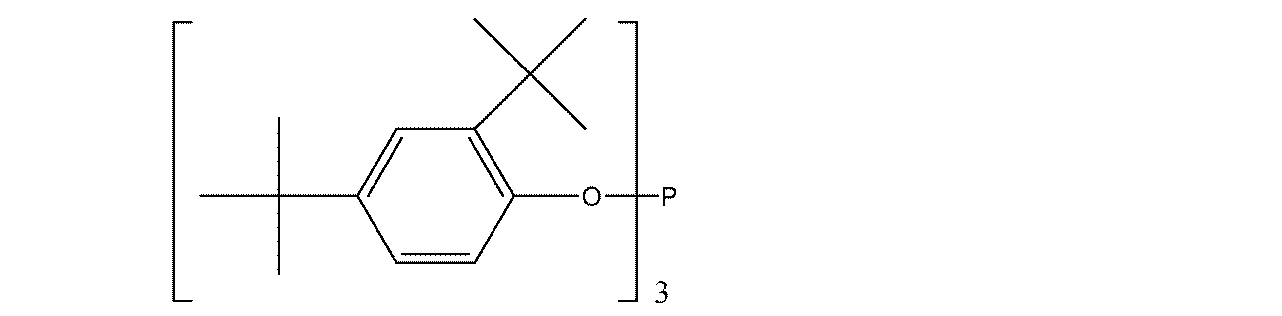
・塗布助剤(メガファックF-780F、DIC株式会社製、下記組成)
界面活性剤 30質量%
メチルエチルケトン 70質量%
界面活性剤 30質量%
メチルエチルケトン 70質量%
・アクリル樹脂溶液(下記組成)
ベンジルメタクリレート/メタクリル酸ランダム共重合体
(モル比78/22、重量平均分子量 38,000) 27質量%
プロピレングリコールモノメチルエーテルアセタート 73質量%
ベンジルメタクリレート/メタクリル酸ランダム共重合体
(モル比78/22、重量平均分子量 38,000) 27質量%
プロピレングリコールモノメチルエーテルアセタート 73質量%
・アクリルモノマー溶液(日本化薬株式会社製、下記組成)
ジペンタエリスリトールヘキサアクリレート 76質量%
プロピレングリコールモノメチルエーテルアセタート 24質量%
ジペンタエリスリトールヘキサアクリレート 76質量%
プロピレングリコールモノメチルエーテルアセタート 24質量%
・重合開始剤(IRGACURE379EG、BASF社製、下記化合物)
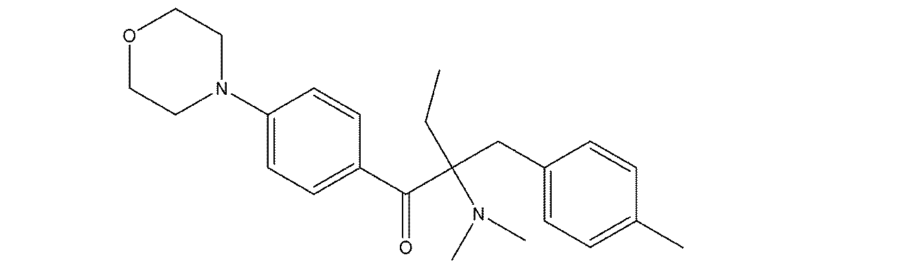
・重合禁止剤(フェノチアジン、下記化合物)

・有機溶媒1(プロピレングリコールモノメチルエーテルアセタート)
・有機溶媒2(メチルエチルケトン)
・有機溶媒3(シクロヘキサノン)
・有機溶媒2(メチルエチルケトン)
・有機溶媒3(シクロヘキサノン)
<加飾材形成用転写材料の作製>
厚さ75μmの仮支持体(ポリエチレンテレフタレートフィルム)の上に、スリット状ノズルを用いて、下記処方H1からなる熱可塑性樹脂層用塗布液を塗布、乾燥させた。次に、下記処方P1からなる中間層用塗布液を塗布、乾燥させた。
厚さ75μmの仮支持体(ポリエチレンテレフタレートフィルム)の上に、スリット状ノズルを用いて、下記処方H1からなる熱可塑性樹脂層用塗布液を塗布、乾燥させた。次に、下記処方P1からなる中間層用塗布液を塗布、乾燥させた。
(熱可塑性樹脂層用塗布液:処方H1)
・メタノール :11.1質量部
・プロピレングリコールモノメチルエーテルアセテート :6.36質量部
・メチルエチルケトン :52.4質量部
・メチルメタクリレート/2-エチルヘキシルアクリレート/ベンジル
メタクリレート/メタクリル酸共重合体(共重合組成比(モル比)=
55/11.7/4.5/28.8、分子量=10万、Tg≒70℃)
:5.83質量部
・スチレン/アクリル酸共重合体(共重合組成比(モル比)=63/37、
重量平均分子量=1万、Tg≒100℃) :13.6質量部
・モノマー1(商品名:BPE-500、新中村化学工業(株)製)
:9.1質量部
・塗布助剤 :0.54質量部
なお、熱可塑性樹脂層用塗布液H1の溶剤除去後の120℃の粘度は1500Pa・secであった。
・メタノール :11.1質量部
・プロピレングリコールモノメチルエーテルアセテート :6.36質量部
・メチルエチルケトン :52.4質量部
・メチルメタクリレート/2-エチルヘキシルアクリレート/ベンジル
メタクリレート/メタクリル酸共重合体(共重合組成比(モル比)=
55/11.7/4.5/28.8、分子量=10万、Tg≒70℃)
:5.83質量部
・スチレン/アクリル酸共重合体(共重合組成比(モル比)=63/37、
重量平均分子量=1万、Tg≒100℃) :13.6質量部
・モノマー1(商品名:BPE-500、新中村化学工業(株)製)
:9.1質量部
・塗布助剤 :0.54質量部
なお、熱可塑性樹脂層用塗布液H1の溶剤除去後の120℃の粘度は1500Pa・secであった。
(中間層用塗布液:処方P1)
・ポリビニルアルコール :32.2質量部
(商品名:PVA205、(株)クラレ製、鹸化度=88%、重合度550)
・ポリビニルピロリドン :14.9質量部
(商品名:K-30、アイエスピー・ジャパン(株)製)
・蒸留水 :524質量部
・メタノール :429質量部
・ポリビニルアルコール :32.2質量部
(商品名:PVA205、(株)クラレ製、鹸化度=88%、重合度550)
・ポリビニルピロリドン :14.9質量部
(商品名:K-30、アイエスピー・ジャパン(株)製)
・蒸留水 :524質量部
・メタノール :429質量部
中間層用塗布液を塗布、乾燥させた中間膜の上に、更に、上記表1中の、黒色着色液1~4、及び白色着色液1~2を、各々塗布、乾燥させて、遮光層および白色着色層を形成した。
仮支持体の上に乾燥膜厚が15.1μmの熱可塑性樹脂層と、乾燥膜厚が1.6μmの中間層と、乾燥膜厚が、1.6~2.7μmの遮光層、35μmの白色着色層を各々設けた後、白色着色層上に最後に保護フィルム(厚さ12μmポリプロピレンフィルム)を圧着した。
こうして仮支持体と熱可塑性樹脂層と中間層(酸素遮断膜)と遮光層および白色着色層とが一体となった下記表2に記載の白色転写材料1、2および黒色転写材料1~4を作製した。
各転写材料の白色着色層および遮光層の膜厚と光学濃度を測定した。結果を以下の表2に示す。膜厚測定は、テンコールインストルメンツ社製 P-10を用いて行った。光学濃度は、サカタインクス株式会社製 BMT-1を用いて測定を行った。
仮支持体の上に乾燥膜厚が15.1μmの熱可塑性樹脂層と、乾燥膜厚が1.6μmの中間層と、乾燥膜厚が、1.6~2.7μmの遮光層、35μmの白色着色層を各々設けた後、白色着色層上に最後に保護フィルム(厚さ12μmポリプロピレンフィルム)を圧着した。
こうして仮支持体と熱可塑性樹脂層と中間層(酸素遮断膜)と遮光層および白色着色層とが一体となった下記表2に記載の白色転写材料1、2および黒色転写材料1~4を作製した。
各転写材料の白色着色層および遮光層の膜厚と光学濃度を測定した。結果を以下の表2に示す。膜厚測定は、テンコールインストルメンツ社製 P-10を用いて行った。光学濃度は、サカタインクス株式会社製 BMT-1を用いて測定を行った。

<フィルム転写法による加飾材付基材の作製>
図2のような開口部(15mmΦ)が形成された強化処理ガラス(300mm×400mm×0.7mm)を、25℃に調整したガラス洗浄剤液をシャワーにより20秒間吹き付けながらナイロン毛を有する回転ブラシで洗浄した。このガラス基板を基材予備加熱装置で50℃、2分間予備加熱した。
図2のような開口部(15mmΦ)が形成された強化処理ガラス(300mm×400mm×0.7mm)を、25℃に調整したガラス洗浄剤液をシャワーにより20秒間吹き付けながらナイロン毛を有する回転ブラシで洗浄した。このガラス基板を基材予備加熱装置で50℃、2分間予備加熱した。
上記のガラス基板上に、作製例1の白色転写材料1をガラス基板の四辺に対応するサイズの額縁状に成形した後で転写した。詳細を以下に示す。
まず、作製例1の白色転写材料1を、ガラス基板の四辺に対応するサイズになるように、額縁状に裁断加工した。
次いで、裁断後の白色転写材料1から、保護フィルムを剥離した。
その後、保護フィルムを剥離することにより露出した白色着色層の表面と、前記50℃で予備加熱したガラス基板の表面とが接するように重ね合わせ、ラミネータ((株)日立インダストリイズ製(LamicII型))を用いて、ゴムローラー温度50℃、線圧100N/cm、搬送速度2.5m/分でラミネートした。続いて仮支持体を、熱可塑性樹脂層との界面で剥離し、仮支持体を除去した。
次に、トリエタノールアミン系現像液(トリエタノールアミン30質量%含有、商品名:T-PD2(富士フイルム(株)製)を純水で10倍に希釈した液)を用いて、30℃で60秒間、フラットノズル圧力0.1MPaでシャワー現像し、熱可塑性樹脂層と中間層とを除去して、白色着色層付基材を作成した。引き続き、得られた基材の上面にエアを吹きかけて液切りした後、純水をシャワーにより10秒間吹き付けて純水シャワー洗浄し、その後、エアを吹きかけて基材上の液だまりを減らした。
次いで、白色着色層を硬化するため、ガラス基板(基材)ごと、150℃30分加熱した。
まず、作製例1の白色転写材料1を、ガラス基板の四辺に対応するサイズになるように、額縁状に裁断加工した。
次いで、裁断後の白色転写材料1から、保護フィルムを剥離した。
その後、保護フィルムを剥離することにより露出した白色着色層の表面と、前記50℃で予備加熱したガラス基板の表面とが接するように重ね合わせ、ラミネータ((株)日立インダストリイズ製(LamicII型))を用いて、ゴムローラー温度50℃、線圧100N/cm、搬送速度2.5m/分でラミネートした。続いて仮支持体を、熱可塑性樹脂層との界面で剥離し、仮支持体を除去した。
次に、トリエタノールアミン系現像液(トリエタノールアミン30質量%含有、商品名:T-PD2(富士フイルム(株)製)を純水で10倍に希釈した液)を用いて、30℃で60秒間、フラットノズル圧力0.1MPaでシャワー現像し、熱可塑性樹脂層と中間層とを除去して、白色着色層付基材を作成した。引き続き、得られた基材の上面にエアを吹きかけて液切りした後、純水をシャワーにより10秒間吹き付けて純水シャワー洗浄し、その後、エアを吹きかけて基材上の液だまりを減らした。
次いで、白色着色層を硬化するため、ガラス基板(基材)ごと、150℃30分加熱した。
次いで、硬化した白色着色層の上に作製例2の黒色転写材料1を転写し、白色転写材料1と同様に仮支持体、熱可塑性樹脂層と中間層を除去した。次いで、ITOスパッタを想定した、280℃30分の加熱を行い、ガラス基板、白色着色層、遮光層がこの順で積層された実施例1の加飾材付き基材を得た。
実施例1において、用いた白色転写材料および黒色転写材料を下記表3に記載のとおりに変更した以外は実施例1と同様に、ガラス基板上に白色着色層および遮光層が形成された実施例2、3、及び比較例1の加飾材付き基材を得た。
<評価>
上記で得た各実施例および比較例の加飾材付き基材の特性の評価方法を以下に示す。
また、得られた結果を下記表3にそれぞれ記載した。
上記で得た各実施例および比較例の加飾材付き基材の特性の評価方法を以下に示す。
また、得られた結果を下記表3にそれぞれ記載した。
(高温処理後の明度および色味)
上記で作製した各実施例および比較例の加飾材付き基材に対し、280℃で30分間加熱した。
得られた高温処理後の加飾材付き基材の基材側から黒紙を下敷きとして、X-Rite社製938 Spectrodensitometerを用いて測定を行ない、L値を求めた。
また、高温処理後の加飾材付き基材の色味を、測色計(CM-700d、コニカミノルタセンシング株式会社製、SCIモード、D65光源、10°測定)を用いて、基材側から測定し、b値を求めた。
上記で作製した各実施例および比較例の加飾材付き基材に対し、280℃で30分間加熱した。
得られた高温処理後の加飾材付き基材の基材側から黒紙を下敷きとして、X-Rite社製938 Spectrodensitometerを用いて測定を行ない、L値を求めた。
また、高温処理後の加飾材付き基材の色味を、測色計(CM-700d、コニカミノルタセンシング株式会社製、SCIモード、D65光源、10°測定)を用いて、基材側から測定し、b値を求めた。
(光学濃度)
上記で作製した各実施例および比較例の加飾材付き基材の光学濃度を、サカタインクス株式会社製 BMT-1を用いて測定した。
上記で作製した各実施例および比較例の加飾材付き基材の光学濃度を、サカタインクス株式会社製 BMT-1を用いて測定した。
(遮光層上の表面抵抗)
上記で作製した各実施例および比較例の加飾材付き基材の遮光層上の表面抵抗を、株式会社アドバンテスト製、R8340A ULTRA HIGH RESISTANCE METERを用いて測定した。
上記で作製した各実施例および比較例の加飾材付き基材の遮光層上の表面抵抗を、株式会社アドバンテスト製、R8340A ULTRA HIGH RESISTANCE METERを用いて測定した。
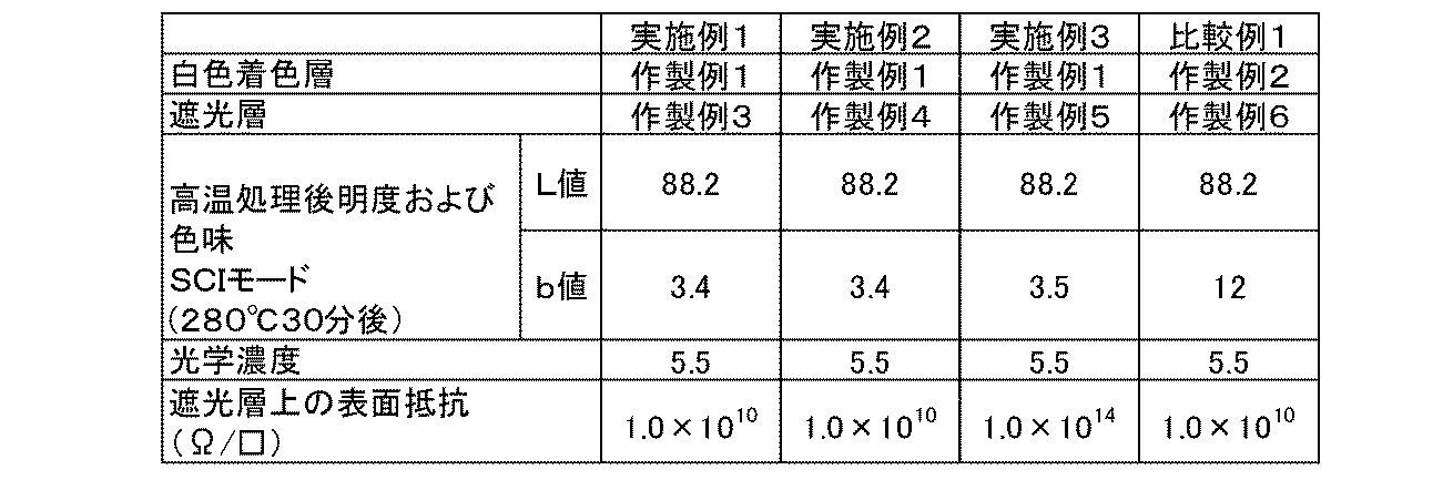
上記表3より、シロキサン結合を主鎖に有する樹脂を白色着色層および遮光層のいずれにも用いた加飾材付き基材(実施例1~3)では、高温処理後のb値が小さく、見栄えとして黄色味が目立たず、白色加飾材として好ましいものであった。
対してシロキサン結合を主鎖に有する樹脂を含まない加飾材付き基材(比較例1)では、高温処理後のb値が大きく、見栄えとして黄色味が目立ち、白色加飾材として好ましくないものであった。
対してシロキサン結合を主鎖に有する樹脂を含まない加飾材付き基材(比較例1)では、高温処理後のb値が大きく、見栄えとして黄色味が目立ち、白色加飾材として好ましくないものであった。
[実施例101:タッチパネルの作製]
《第一の透明電極パターンの形成》
<透明電極層の形成>
各実施例の加飾材付き基材を、真空チャンバー内に導入し、SnO2含有率が10質量%のITOターゲット(インジウム:錫=95:5(モル比))を用いて、DCマグネトロンスパッタリング(条件:基材の温度250℃、アルゴン圧0.13Pa、酸素圧0.01Pa)により、厚さ40nmのITO薄膜を形成し、透明電極層を形成した前面板を得た。ITO薄膜の表面抵抗は80Ω/□であった。
《第一の透明電極パターンの形成》
<透明電極層の形成>
各実施例の加飾材付き基材を、真空チャンバー内に導入し、SnO2含有率が10質量%のITOターゲット(インジウム:錫=95:5(モル比))を用いて、DCマグネトロンスパッタリング(条件:基材の温度250℃、アルゴン圧0.13Pa、酸素圧0.01Pa)により、厚さ40nmのITO薄膜を形成し、透明電極層を形成した前面板を得た。ITO薄膜の表面抵抗は80Ω/□であった。
<エッチング用転写フィルムE1の調製>
前記作製例1の白色転写材料1の調製において、前記白色着色液1を、下記処方E1からなるエッチング用光硬化性樹脂層用塗布液に代えた以外は作製例1の白色転写材料1の調製と同様にして、仮支持体、熱可塑性樹脂層、中間層(酸素遮断膜)、エッチング用光硬化性樹脂層および保護フィルムとが一体となった、エッチング用転写フィルムE1を得た(エッチング用光硬化性樹脂層の膜厚は2.0μmであった)。
前記作製例1の白色転写材料1の調製において、前記白色着色液1を、下記処方E1からなるエッチング用光硬化性樹脂層用塗布液に代えた以外は作製例1の白色転写材料1の調製と同様にして、仮支持体、熱可塑性樹脂層、中間層(酸素遮断膜)、エッチング用光硬化性樹脂層および保護フィルムとが一体となった、エッチング用転写フィルムE1を得た(エッチング用光硬化性樹脂層の膜厚は2.0μmであった)。
(エッチング用光硬化性樹脂層用塗布液:処方E1)
・メチルメタクリレート/スチレン/メタクリル酸共重合体
(共重合体組成(質量%):31/40/29、質量平均分子量60000、
酸価163mgKOH/g) :16質量部
・モノマー1(商品名:BPE-500、新中村化学工業(株)製) :5.6質量部
・ヘキサメチレンジイソシアネートのテトラエチレンオキシドモノ
メタクリレート0.5モル付加物 :7質量部
・分子中に重合性基を1つ有する化合物としてのシクロヘキサンジ
メタノールモノアクリレート :2.8質量部
・2-クロロ-N-ブチルアクリドン :0.42質量部
・2,2-ビス(o-クロロフェニル)-4,4’,5,5’-テトラフェニル
ビイミダゾール :2.17質量部
・ロイコクリスタルバイオレット :0.26質量部
・フェノチアジン :0.013質量部
・界面活性剤(商品名:メガファックF-780F、大日本インキ(株)製)
:0.03質量部
・メチルエチルケトン :40質量部
・1-メトキシ-2-プロパノール :20質量部
・メチルメタクリレート/スチレン/メタクリル酸共重合体
(共重合体組成(質量%):31/40/29、質量平均分子量60000、
酸価163mgKOH/g) :16質量部
・モノマー1(商品名:BPE-500、新中村化学工業(株)製) :5.6質量部
・ヘキサメチレンジイソシアネートのテトラエチレンオキシドモノ
メタクリレート0.5モル付加物 :7質量部
・分子中に重合性基を1つ有する化合物としてのシクロヘキサンジ
メタノールモノアクリレート :2.8質量部
・2-クロロ-N-ブチルアクリドン :0.42質量部
・2,2-ビス(o-クロロフェニル)-4,4’,5,5’-テトラフェニル
ビイミダゾール :2.17質量部
・ロイコクリスタルバイオレット :0.26質量部
・フェノチアジン :0.013質量部
・界面活性剤(商品名:メガファックF-780F、大日本インキ(株)製)
:0.03質量部
・メチルエチルケトン :40質量部
・1-メトキシ-2-プロパノール :20質量部
<第一の透明電極パターンの形成>
白色着色層、遮光層、透明電極層を形成した前面板を、25℃に調整したガラス洗浄剤液をシャワーにより20秒間吹き付けながらナイロン毛を有する回転ブラシで洗浄した。次いで、洗浄後の前面板に、保護フィルムを除去したエッチング用転写フィルムE1をラミネートした(基材温度:130℃、ゴムローラー温度120℃、線圧100N/cm、搬送速度2.2m/分)。仮支持体を剥離後、露光マスク(透明電極パターンを有す石英露光マスク)面と該エッチング用光硬化性樹脂層との間の距離を200μmに設定し、露光量50mJ/cm2(i線)でパターン露光した。
次に、トリエタノールアミン系現像液(トリエタノールアミン30質量%含有、商品名:T-PD2(富士フイルム(株)製)を純水で10倍に希釈した液)を用いて25℃で100秒間処理した。続いて、界面活性剤含有洗浄液(商品名:T-SD3(富士フイルム(株)製)を純水で10倍に希釈した液)を用いて33℃で20秒間処理して残渣除去を行い、さらに130℃、30分間のポストベーク処理を行って、白色着色層、遮光層、透明電極層とエッチング用光硬化性樹脂層パターンとを形成した前面板を得た。
白色着色層、遮光層、透明電極層を形成した前面板を、25℃に調整したガラス洗浄剤液をシャワーにより20秒間吹き付けながらナイロン毛を有する回転ブラシで洗浄した。次いで、洗浄後の前面板に、保護フィルムを除去したエッチング用転写フィルムE1をラミネートした(基材温度:130℃、ゴムローラー温度120℃、線圧100N/cm、搬送速度2.2m/分)。仮支持体を剥離後、露光マスク(透明電極パターンを有す石英露光マスク)面と該エッチング用光硬化性樹脂層との間の距離を200μmに設定し、露光量50mJ/cm2(i線)でパターン露光した。
次に、トリエタノールアミン系現像液(トリエタノールアミン30質量%含有、商品名:T-PD2(富士フイルム(株)製)を純水で10倍に希釈した液)を用いて25℃で100秒間処理した。続いて、界面活性剤含有洗浄液(商品名:T-SD3(富士フイルム(株)製)を純水で10倍に希釈した液)を用いて33℃で20秒間処理して残渣除去を行い、さらに130℃、30分間のポストベーク処理を行って、白色着色層、遮光層、透明電極層とエッチング用光硬化性樹脂層パターンとを形成した前面板を得た。
白色着色層、遮光層、透明電極層とエッチング用光硬化性樹脂層パターンとを形成した前面板を、ITOエッチャント(塩酸、塩化カリウム水溶液。液温30℃)を入れたエッチング槽に浸漬し、100秒処理し、エッチング用光硬化性樹脂層で覆われていない露出した領域の透明電極層を溶解除去し、白色着色層、遮光層、エッチング用光硬化性樹脂層パターンのついた透明電極層パターン付の前面板を得た。
次に、エッチング用光硬化性樹脂層パターンのついた透明電極層パターン付の前面板を、レジスト剥離液(N-メチル-2-ピロリドン、モノエタノールアミン、界面活性剤(商品名:サーフィノール465、エアープロダクツ製)液温45℃)を入れたレジスト剥離槽に浸漬し、200秒処理し、エッチング用光硬化性樹脂層を除去し、白色着色層と、遮光層と、前記前面板の非接触面および前記遮光層の前記前面板側とは逆側の面の両方の領域にまたがって図1Aのように設置された第一の透明電極パターンとを形成した前面板を得た。
《絶縁層の形成》
<絶縁層形成用転写フィルムW1の調製>
作製例1の白色転写材料1の調製において、前記白色着色液1を、下記処方W1からなる絶縁層形成用塗布液に代えた以外は作製例1の白色転写材料1の調製と同様にして、仮支持体、熱可塑性樹脂層、中間層(酸素遮断膜)、絶縁層用光硬化性樹脂層および保護フィルムとが一体となった、絶縁層形成用転写フィルムW1を得た(絶縁層用光硬化性樹脂層の膜厚は1.4μm)。
<絶縁層形成用転写フィルムW1の調製>
作製例1の白色転写材料1の調製において、前記白色着色液1を、下記処方W1からなる絶縁層形成用塗布液に代えた以外は作製例1の白色転写材料1の調製と同様にして、仮支持体、熱可塑性樹脂層、中間層(酸素遮断膜)、絶縁層用光硬化性樹脂層および保護フィルムとが一体となった、絶縁層形成用転写フィルムW1を得た(絶縁層用光硬化性樹脂層の膜厚は1.4μm)。
(絶縁層形成用塗布液:処方W1)
・バインダー3(シクロヘキシルメタクリレート(a)/メチルメタクリレート(b)/メタクリル酸共重合体(c)のグリシジルメタクリレート付加物(d)(組成(質量%):a/b/c/d=46/1/10/43、質量平均分子量:36000、酸価66mgKOH/g)の1-メトキシ-2-プロパノール、メチルエチルケトン溶液(固形分:45%)) :12.5質量部
・DPHA(ジペンタエリスリトールヘキサアクリレート、日本化薬(株)製)
のプロピレングリコールモノメチルエーテルアセテート溶液(76質量%)
:1.4質量部
・ウレタン系モノマー(商品名:NKオリゴUA-32P、新中村化学(株)製
:不揮発分75%、プロピレングリコールモノメチルエーテルアセテート:
25%) :0.68質量部
・トリペンタエリスリトールオクタアクリレート(商品名:V#802、
大阪有機化学工業(株)製) :1.8質量部
・ジエチルチオキサントン :0.17質量部
・2-(ジメチルアミノ)-2-[(4-メチルフェニル)メチル]-1-
[4-(4-モルホリニル)フェニル]-1-ブタノン
(商品名:Irgacure379、BASF製) :0.17質量部
・分散剤(商品名:ソルスパース20000、アビシア製) :0.19質量部
・界面活性剤(商品名:メガファックF-780F、大日本インキ製)
:0.05質量部
・メチルエチルケトン :23.3質量部
・MMPGAc(ダイセル化学(株)製) :59.8質量部
なお、絶縁層形成用塗布液W1の溶剤除去後の100℃の粘度は4000Pa・secであった。
・バインダー3(シクロヘキシルメタクリレート(a)/メチルメタクリレート(b)/メタクリル酸共重合体(c)のグリシジルメタクリレート付加物(d)(組成(質量%):a/b/c/d=46/1/10/43、質量平均分子量:36000、酸価66mgKOH/g)の1-メトキシ-2-プロパノール、メチルエチルケトン溶液(固形分:45%)) :12.5質量部
・DPHA(ジペンタエリスリトールヘキサアクリレート、日本化薬(株)製)
のプロピレングリコールモノメチルエーテルアセテート溶液(76質量%)
:1.4質量部
・ウレタン系モノマー(商品名:NKオリゴUA-32P、新中村化学(株)製
:不揮発分75%、プロピレングリコールモノメチルエーテルアセテート:
25%) :0.68質量部
・トリペンタエリスリトールオクタアクリレート(商品名:V#802、
大阪有機化学工業(株)製) :1.8質量部
・ジエチルチオキサントン :0.17質量部
・2-(ジメチルアミノ)-2-[(4-メチルフェニル)メチル]-1-
[4-(4-モルホリニル)フェニル]-1-ブタノン
(商品名:Irgacure379、BASF製) :0.17質量部
・分散剤(商品名:ソルスパース20000、アビシア製) :0.19質量部
・界面活性剤(商品名:メガファックF-780F、大日本インキ製)
:0.05質量部
・メチルエチルケトン :23.3質量部
・MMPGAc(ダイセル化学(株)製) :59.8質量部
なお、絶縁層形成用塗布液W1の溶剤除去後の100℃の粘度は4000Pa・secであった。
前記白色着色層、遮光層、第一の透明電極パターン付の前面板を、25℃に調整したガラス洗浄剤液をシャワーにより20秒間吹き付けながらナイロン毛を有する回転ブラシで洗浄した。次いで、洗浄後の前面板に、保護フィルムを除去した絶縁層形成用転写フィルムW1をラミネートした(基材温度:100℃、ゴムローラー温度120℃、線圧100N/cm、搬送速度2.3m/分)。仮支持体を剥離後、露光マスク(絶縁層用パターンを有す石英露光マスク)面と該絶縁層形成用光硬化性樹脂層との間の距離を100μmに設定し、露光量30mJ/cm2(i線)でパターン露光した。
次に、トリエタノールアミン系現像液(トリエタノールアミン30質量%含有、商品名:T-PD2(富士フイルム(株)製)を純水で10倍に希釈した液)を用いて33℃で60秒間処理し、続いて、炭酸ナトリウム/炭酸水素ナトリウム系現像液(商品名:T-CD1(富士フイルム(株)製)を純水で5倍に希釈した液)を用いて25℃で50秒間処理した。その後、界面活性剤含有洗浄液(商品名:T-SD3(富士フイルム(株)製)を純水で10倍に希釈した液)を用いて33℃で20秒間処理して残渣除去を行い、さらに230℃、60分間のポストベーク処理を行って、白色着色層、遮光層、第一の透明電極パターン、絶縁層パターンを形成した前面板を得た。
《第二の透明電極パターンの形成》
<透明電極層の形成>
前記第一の透明電極パターンの形成と同様にして、白色着色層、遮光層、第一の透明電極パターン、絶縁層パターンを形成した前面板をDCマグネトロンスパッタリング処理し(条件:基材の温度50℃、アルゴン圧0.13Pa、酸素圧0.01Pa)、厚さ80nmのITO薄膜を形成し、白色着色層、遮光層、第一の透明電極パターン、絶縁層パターン、透明電極層を形成した前面板を得た。ITO薄膜の表面抵抗は110Ω/□であった。
<透明電極層の形成>
前記第一の透明電極パターンの形成と同様にして、白色着色層、遮光層、第一の透明電極パターン、絶縁層パターンを形成した前面板をDCマグネトロンスパッタリング処理し(条件:基材の温度50℃、アルゴン圧0.13Pa、酸素圧0.01Pa)、厚さ80nmのITO薄膜を形成し、白色着色層、遮光層、第一の透明電極パターン、絶縁層パターン、透明電極層を形成した前面板を得た。ITO薄膜の表面抵抗は110Ω/□であった。
第一の透明電極パターンの形成と同様にして、エッチング用転写フィルムE1を用いて、白色着色層、遮光層、第一の透明電極パターン、絶縁層パターン、透明電極層、エッチング用光硬化性樹脂層パターンを形成した前面板を得た(ポストベーク処理;130℃、30分間)。
さらに、第一の透明電極パターンの形成と同様にして、エッチング(30℃、50秒間)して、エッチング用光硬化性樹脂層を除去(45℃、200秒間)することにより、白色着色層、遮光層、第一の透明電極パターン、絶縁層パターン、前記前面板の非接触面および前記遮光層の前記前面板側とは逆側の面の両方の領域にまたがって図1Aのように設置された第二の透明電極パターンを形成した前面板を得た。
さらに、第一の透明電極パターンの形成と同様にして、エッチング(30℃、50秒間)して、エッチング用光硬化性樹脂層を除去(45℃、200秒間)することにより、白色着色層、遮光層、第一の透明電極パターン、絶縁層パターン、前記前面板の非接触面および前記遮光層の前記前面板側とは逆側の面の両方の領域にまたがって図1Aのように設置された第二の透明電極パターンを形成した前面板を得た。
《第一および第二の透明電極パターンとは別の導電性要素の形成》
前記第一、および第二の透明電極パターンの形成と同様にして、白色着色層、遮光層、第一の透明電極パターン、絶縁層パターン、第二の透明電極パターンを形成した前面板をDCマグネトロンスパッタリング処理し、厚さ200nmのアルミニウム(Al)薄膜を形成した前面板を得た。
前記第一、および第二の透明電極パターンの形成と同様にして、白色着色層、遮光層、第一の透明電極パターン、絶縁層パターン、第二の透明電極パターンを形成した前面板をDCマグネトロンスパッタリング処理し、厚さ200nmのアルミニウム(Al)薄膜を形成した前面板を得た。
前記第一、および第二の透明電極パターンの形成と同様にして、エッチング用転写フィルムE1を用いて、白色着色層、遮光層、第一の透明電極パターン、絶縁層パターン、第二の透明電極パターン、アルミニウム薄膜、エッチング用光硬化性樹脂層パターンを形成した前面板を得た(ポストベーク処理;130℃、30分間)。
さらに、第一の透明電極パターンの形成と同様にして、エッチング(30℃、50秒間)して、エッチング用光硬化性樹脂層を除去(45℃、200秒間)することにより、白色着色層、遮光層、第一の透明電極パターン、絶縁層パターン、第二の透明電極パターン、第一および第二の透明電極パターンとは別の導電性要素(アルミニウム薄膜)を形成した前面板を得た。
さらに、第一の透明電極パターンの形成と同様にして、エッチング(30℃、50秒間)して、エッチング用光硬化性樹脂層を除去(45℃、200秒間)することにより、白色着色層、遮光層、第一の透明電極パターン、絶縁層パターン、第二の透明電極パターン、第一および第二の透明電極パターンとは別の導電性要素(アルミニウム薄膜)を形成した前面板を得た。
《透明保護層の形成》
絶縁層の形成と同様にして、前記第一および第二の透明電極パターンとは別の導電性要素まで形成した前面板に、保護フィルムを除去した絶縁層形成用転写フィルムW1をラミネートし、仮支持体を剥離後、露光マスクを介さずに露光量50mJ/cm2(i線)で前面露光し、現像、ポスト露光(1000mJ/cm2)、ポストベーク処理を行って、白色着色層、遮光層、第一の透明電極パターン、絶縁層パターン、第二の透明電極パターン、第一および第二の透明電極パターンとは別の導電性要素の全てを覆うように絶縁層(透明保護層)を図1Aのように積層した前面板1を得た。得られた前面板1を実施例1の静電容量型入力装置とした。
絶縁層の形成と同様にして、前記第一および第二の透明電極パターンとは別の導電性要素まで形成した前面板に、保護フィルムを除去した絶縁層形成用転写フィルムW1をラミネートし、仮支持体を剥離後、露光マスクを介さずに露光量50mJ/cm2(i線)で前面露光し、現像、ポスト露光(1000mJ/cm2)、ポストベーク処理を行って、白色着色層、遮光層、第一の透明電極パターン、絶縁層パターン、第二の透明電極パターン、第一および第二の透明電極パターンとは別の導電性要素の全てを覆うように絶縁層(透明保護層)を図1Aのように積層した前面板1を得た。得られた前面板1を実施例1の静電容量型入力装置とした。
《画像表示装置(タッチパネル)の作製》
特開2009-47936公報に記載の方法で製造した液晶表示素子に、先に製造した前面板1(実施例1の静電容量型入力装置)を貼り合せ、公知の方法で静電容量型入力装置を構成要素として備えた実施例1の画像表示装置1を作製した。
特開2009-47936公報に記載の方法で製造した液晶表示素子に、先に製造した前面板1(実施例1の静電容量型入力装置)を貼り合せ、公知の方法で静電容量型入力装置を構成要素として備えた実施例1の画像表示装置1を作製した。
《前面板1、および画像表示装置1の全体評価》
上述の各工程において、白色着色層、遮光層、第一の透明電極パターン、絶縁層パターン、第二の透明電極パターン、第一および第二の透明電極パターンとは別の導電性要素を形成した前面板1(実施例1の静電容量型入力装置)は、開口部、および裏面に汚れがなく、洗浄が容易であり、かつ、他部材の汚染の問題がなかった。
また、白色着色層にはピンホールがなく、白色度、ムラも問題なかった。遮光層には同様にピンホールがなく、光遮蔽性に優れていた。
そして、第一の透明電極パターン、第二の透明電極パターン、およびこれらとは別の導電性要素の、各々の導電性には問題がなく、一方で、第一の透明電極パターンと第二の透明電極パターンの間では絶縁性を有していた。
さらに、透明保護層にも気泡等の欠陥がなく、表示特性に優れた画像表示装置が得られた。
上述の各工程において、白色着色層、遮光層、第一の透明電極パターン、絶縁層パターン、第二の透明電極パターン、第一および第二の透明電極パターンとは別の導電性要素を形成した前面板1(実施例1の静電容量型入力装置)は、開口部、および裏面に汚れがなく、洗浄が容易であり、かつ、他部材の汚染の問題がなかった。
また、白色着色層にはピンホールがなく、白色度、ムラも問題なかった。遮光層には同様にピンホールがなく、光遮蔽性に優れていた。
そして、第一の透明電極パターン、第二の透明電極パターン、およびこれらとは別の導電性要素の、各々の導電性には問題がなく、一方で、第一の透明電極パターンと第二の透明電極パターンの間では絶縁性を有していた。
さらに、透明保護層にも気泡等の欠陥がなく、表示特性に優れた画像表示装置が得られた。
(白色着色層、遮光層の積層転写材料)
実施例1~3で作製した仮支持体、熱可塑性樹脂層、中間層上に、実施例1~3で黒色着色液を塗布、乾燥するときと同様に、下記表4に記載の黒色着色液5から9を、ODが4.5となるように、塗布、乾燥した。更に、各々に前記表1に記載の白色着色液1を、乾燥後の膜厚が35μmとなるように塗布、乾燥し、下記表5の白色着色層/遮光層の積層転写材料1から5を得た。
実施例1~3で作製した仮支持体、熱可塑性樹脂層、中間層上に、実施例1~3で黒色着色液を塗布、乾燥するときと同様に、下記表4に記載の黒色着色液5から9を、ODが4.5となるように、塗布、乾燥した。更に、各々に前記表1に記載の白色着色液1を、乾燥後の膜厚が35μmとなるように塗布、乾燥し、下記表5の白色着色層/遮光層の積層転写材料1から5を得た。
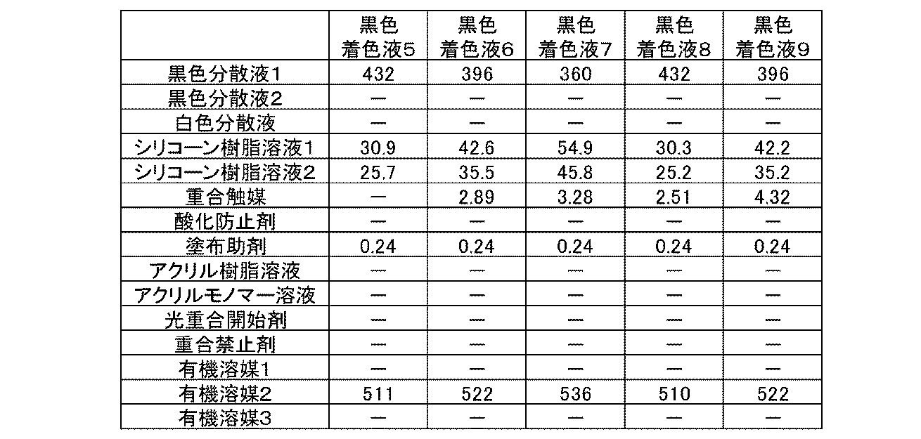
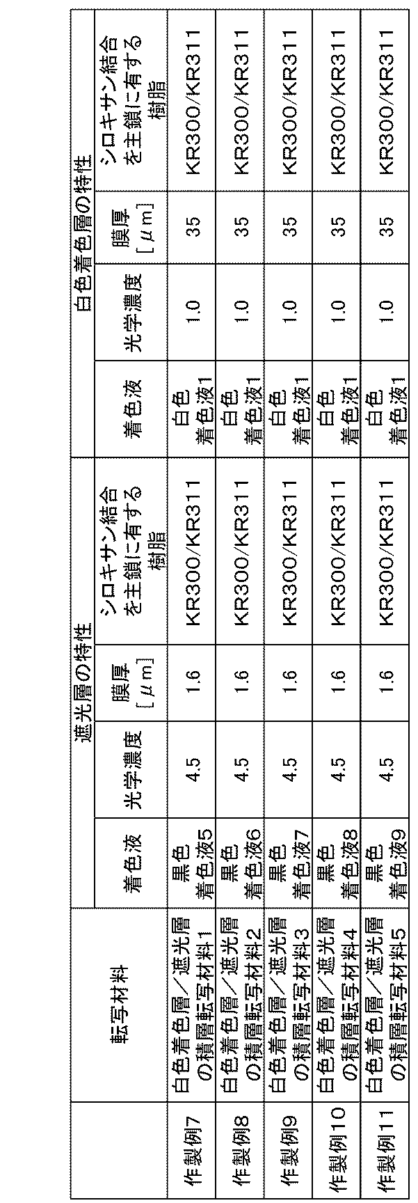
実施例1~3と同様に、ガラス基板上に白色着色層/遮光層の積層転写材料1から5を転写して、ITOスパッタを想定した280℃30分の加熱を行い、実施例4から8の加飾材付き基材を得た。
得られた加飾材付き基材の評価を実施例1~3と同様に行い、下記表6に記載の結果を得た。
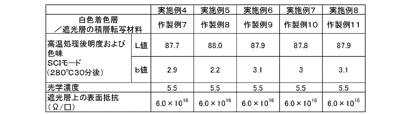
上記表6より、実施例4から8で得られた加飾材付き基材は、何れも好ましいものであった。
[実施例106]
実施例1の加飾材付き基材の代わりに実施例6の加飾材付き基材を用いた以外は実施例101と同様の操作を行い、実施例106の前面板を得た。この前面板は、他の実施例の前面板同様に、好ましいものであった。
実施例1の加飾材付き基材の代わりに実施例6の加飾材付き基材を用いた以外は実施例101と同様の操作を行い、実施例106の前面板を得た。この前面板は、他の実施例の前面板同様に、好ましいものであった。
[実施例201、比較例201]
(熱転写印刷法)
片面に耐熱滑性層を有する厚さ15μmのPETフィルムの、該耐熱滑性層と反対側の面に白色着色液1および2と黒色着色液1および4を、各々乾燥膜厚が9.0μm、9.0μm、1.6μm、2.0μmとなるように塗布乾燥し、熱転写リボン白1および白2、黒1および黒4を得た。
(熱転写印刷法)
片面に耐熱滑性層を有する厚さ15μmのPETフィルムの、該耐熱滑性層と反対側の面に白色着色液1および2と黒色着色液1および4を、各々乾燥膜厚が9.0μm、9.0μm、1.6μm、2.0μmとなるように塗布乾燥し、熱転写リボン白1および白2、黒1および黒4を得た。
ガラス基板上に、熱転写リボン白1を押し当て白色着色液1由来の白色着色層を転写した。これを4回繰り返し、厚さ36μmの白色着色層1を得た。これを、150℃で30分加熱し、硬膜した。この白色着色層1の上に、熱転写リボン黒1を押し当て黒色着色液1由来の遮光層を転写し、実施例201の加飾材付き基材を得た。
また、ガラス基板上に、熱転写リボン白2を押し当て白色着色液2由来の白色着色層を転写した。次に高圧水銀ランプを光源に、i線で100mJ/cm2となるよう露光した。これを4回繰り返し、厚さ36μmの白色着色層2を得た。これを、150℃で30分加熱し、硬膜した。この白色着色層2の上に、熱転写リボン黒2を押し当て黒色着色液4由来の遮光層を転写し、比較例201の加飾材付き基材を得た。
実施例1と同様に、ITOスパッタを想定して、実施例201および比較例201の加飾材付き基材を、窒素雰囲気下、280℃で30分加熱し、高温処理後の色味としてb値を測定した。
実施例201の加飾材付き基材のb値は3.2、比較例201の加飾材付き基材のb値は12であり、(A1)は高温処理後に有意に着色していないことがわかった。
実施例201の加飾材付き基材のb値は3.2、比較例201の加飾材付き基材のb値は12であり、(A1)は高温処理後に有意に着色していないことがわかった。
[実施例301、比較例301]
(インクジェット印刷法)
吐出量1.8pLのインクジェットヘッドを用い、白色着色液1をガラス基板上にインクジェット印刷し、印刷物を150℃30分乾燥した。この操作を、さらに5回繰り返し、厚さ36μmの白色着色層1bを作製した。この白色着色層1bの上に、白色着色層1bの形成と同様にして、黒色着色液1を印刷し、次いで150℃30分乾燥する操作を繰り返して、厚さ2.0μmの遮光層1bを形成し、実施例301の加飾材付き基材を得た。
(インクジェット印刷法)
吐出量1.8pLのインクジェットヘッドを用い、白色着色液1をガラス基板上にインクジェット印刷し、印刷物を150℃30分乾燥した。この操作を、さらに5回繰り返し、厚さ36μmの白色着色層1bを作製した。この白色着色層1bの上に、白色着色層1bの形成と同様にして、黒色着色液1を印刷し、次いで150℃30分乾燥する操作を繰り返して、厚さ2.0μmの遮光層1bを形成し、実施例301の加飾材付き基材を得た。
インク吐出量を調整し、白色着色液2と黒色着色液4を用い、ガラス基板上に厚さ36μmの白色着色層2bと、厚さ2.0μmの遮光層4bよりなる、比較例301の加飾材付き基材を得た。
実施例1と同様に、ITOスパッタを想定して、実施例301および比較例301の加飾材付き基材を、窒素雰囲気下、280℃で30分加熱し、高温処理後の色味としてb値を測定した。
実施例301の加飾材付き基材のb値は3.2、比較例301の加飾材付き基材のb値は12であり、実施例301の加飾材付き基材は高温処理後に有意に着色していないことがわかった。
[実施例401、比較例401]
(スクリーン印刷法)
白色着色液1、2を、各々の有機溶媒1~3の割合を減らすことで、1000mPa・sに調整し、白色着色液1a、2aを調整した。次いで、黒色着色液1、4を、各々の有機溶媒1~3の割合を減らすことで、200mPa・sに調整し、黒色着色液1a、4aを調製した。
(スクリーン印刷法)
白色着色液1、2を、各々の有機溶媒1~3の割合を減らすことで、1000mPa・sに調整し、白色着色液1a、2aを調整した。次いで、黒色着色液1、4を、各々の有機溶媒1~3の割合を減らすことで、200mPa・sに調整し、黒色着色液1a、4aを調製した。
ガラス基板上に、225メッシュ(オープニング径、65μm)、紗厚72μmのポリエステル製スクリーンを用い、白色着色液1aで厚さ18μmの白色着色層1aを作製した。これを繰り返し、厚さ36μmの白色着色層1aを作製した。これを、150℃で30分加熱し、硬膜した。この白色着色層1aの上に、黒色着色液1aを用いて厚さ1.6mmの遮光層1aを積層し、実施例401の加飾材付き基材を得た。
白色着色液1aの代わりに白色着色液2aを用いて36.0μmの白色着色層2aを作製し、黒色着色液1aの代わりに黒色着色液4aを用いて、厚さ1.6μmの遮光層1aの代わりに厚さ2.0μmの遮光層4aを積層することで、比較例401の加飾材付き基材を得た。
実施例1と同様に、ITOスパッタを想定して、実施例401および比較例401の加飾材付き基材を、窒素雰囲気下、280℃で30分加熱し、高温処理後の色味としてb値を測定した。
実施例401の加飾材付き基材のb値は3.2、比較例401の加飾材付き基材のb値は12であり、実施例401の加飾材付き基材は高温処理後に有意に着色していないことがわかった。
1 基材(フィルム基材。フィルム基材のみを前面板としてもよい)
1’ ガラス(カバーガラス。カバーガラスのみを前面板としてもよく、基材とガラスの積層体を前面板としてもよい)
2a 白色着色層
2b 遮光層
3 導電性層(第一の透明電極パターン)
4 導電性層(第二の電極パターン)
5 絶縁層
6 導電性層(他の導電性要素)
7 透明保護層
10 静電容量型入力装置
1’ ガラス(カバーガラス。カバーガラスのみを前面板としてもよく、基材とガラスの積層体を前面板としてもよい)
2a 白色着色層
2b 遮光層
3 導電性層(第一の透明電極パターン)
4 導電性層(第二の電極パターン)
5 絶縁層
6 導電性層(他の導電性要素)
7 透明保護層
10 静電容量型入力装置
Claims (18)
- 基材、白色着色層および遮光層をこの順で含み、
前記白色着色層と前記遮光層がいずれもシロキサン結合を主鎖に有する樹脂を含むことを特徴とする加飾材付き基材。 - 前記遮光層上に、さらに導電性層を有することを特徴とする請求項1に記載の加飾材付き基材。
- 前記導電性層が、インジウムを含むことを特徴とする請求項2に記載の加飾材付き基材。
- 前記遮光層の表面抵抗が、1.0×10¹⁰Ω/□以上であることを特徴とする請求項1~3のいずれか一項に記載の加飾材付き基材。
- 前記白色着色層と前記遮光層がいずれも顔料を含むことを特徴とする請求項1~4のいずれか一項に記載の加飾材付き基材。
- 前記白色着色層中に含まれる前記顔料以外の全成分に対する前記シロキサン結合を主鎖に有する樹脂の割合が90質量%以上であり、かつ、
前記遮光層中に含まれる前記顔料以外の全成分に対する前記シロキサン結合を主鎖に有する樹脂の割合が70質量%以上であることを特徴とする請求項5に記載の加飾材付き基材。 - 前記白色着色層が、酸化チタンを含むことを特徴とする請求項1~6のいずれか一項に記載の加飾材付き基材。
- 前記白色着色層の膜厚が、10μm~40μmであることを特徴とする請求項1~7のいずれか一項に記載の加飾材付き基材。
- 前記遮光層が、酸化チタンおよびカーボンブラックのうち少なくとも一つを含むことを特徴とする請求項1~8のいずれか一項に記載の加飾材付き基材。
- 前記遮光層の膜厚が、1.0μm~5.0μmであることを特徴とする請求項1~9のいずれか一項に記載の加飾材付き基材。
- 加飾材付き基材の光学濃度が、3.5~6.0であることを特徴とする請求項1~10のいずれか一項に記載の加飾材付き基材。
- 加飾材付き基材の前記基材側の色味が、SCI指標で、L値が85~95、b値が1.5~4.0であることを特徴とする請求項1~11のいずれか一項に記載の加飾材付き基材。
- 前記基材が、ガラス、シクロオレフィンポリマーまたはシリコーン樹脂からなることを特徴とする請求項1~12のいずれか一項に記載の加飾材付き基材。
- 前記シリコーン樹脂が籠型ポリオルガノシルセスキオキサンを主成分とすることを特徴とする請求項13に記載の加飾材付き基材。
- 基材上に白色着色層および遮光層をこの順で積層する工程を含み、
前記白色着色層および前記遮光層が、それぞれ下記の方法から選択される方法で作成され、該方法において用いる白色着色層、遮光層、白色着色層形成用組成物および遮光層形成用組成物が、いずれもシロキサン結合を主鎖に有する樹脂を含むことを特徴とする加飾材付き基材の製造方法。
仮支持体上に少なくとも白色着色層および遮光層の一方を含むフィルム転写材料から少なくとも該白色着色層および該遮光層の一方を転写した後に該仮支持体を取り除く方法
仮支持体上に少なくとも白色着色層および遮光層の一方を含む熱転写材料の該仮支持体側を加熱して、該仮支持体から少なくとも該白色着色層および該遮光層の一方を転写する熱転写印刷
白色着色層形成用組成物または遮光層形成用組成物のスクリーン印刷、および、
白色着色層形成用組成物または遮光層形成用組成物のインクジェット印刷 - 前記白色着色層および前記遮光層を、
少なくとも仮支持体、遮光層および白色着色層の順に含むフィルム転写材料から該遮光層および該白色着色層を、前記基材上に転写した後に該仮支持体を取り除くこと、あるいは、
仮支持体および白色着色層を有するフィルム転写材料から該白色着色層を基材上に転写した後に該仮支持体を取り除き、さらに少なくとも仮支持体および遮光層を含むフィルム転写材料から該遮光層を前記白色着色層上に転写した後に該仮支持体を取り除くこと、
により形成することを特徴とする請求項15に記載の加飾材付き基材の製造方法。 - 請求項1~14のいずれか一項に記載の加飾材付き基材を含むことを特徴とするタッチパネル。
- 請求項17に記載のタッチパネルを有することを特徴とする情報表示装置。
Priority Applications (1)
| Application Number | Priority Date | Filing Date | Title |
|---|---|---|---|
| CN201380057274.8A CN104756052B (zh) | 2012-12-20 | 2013-11-20 | 带有装饰材料的基材以及其制造方法、触摸屏以及信息显示装置 |
Applications Claiming Priority (4)
| Application Number | Priority Date | Filing Date | Title |
|---|---|---|---|
| JP2012278387 | 2012-12-20 | ||
| JP2012-278387 | 2012-12-20 | ||
| JP2013184469A JP5857013B2 (ja) | 2012-12-20 | 2013-09-05 | 加飾材付き基材およびその製造方法、タッチパネルならびに情報表示装置 |
| JP2013-184469 | 2013-09-05 |
Publications (1)
| Publication Number | Publication Date |
|---|---|
| WO2014097803A1 true WO2014097803A1 (ja) | 2014-06-26 |
Family
ID=50978146
Family Applications (1)
| Application Number | Title | Priority Date | Filing Date |
|---|---|---|---|
| PCT/JP2013/081232 Ceased WO2014097803A1 (ja) | 2012-12-20 | 2013-11-20 | 加飾材付き基材およびその製造方法、タッチパネルならびに情報表示装置 |
Country Status (4)
| Country | Link |
|---|---|
| JP (1) | JP5857013B2 (ja) |
| CN (1) | CN104756052B (ja) |
| TW (1) | TWI587187B (ja) |
| WO (1) | WO2014097803A1 (ja) |
Cited By (5)
| Publication number | Priority date | Publication date | Assignee | Title |
|---|---|---|---|---|
| WO2015133599A1 (ja) * | 2014-03-07 | 2015-09-11 | 富士フイルム株式会社 | 加飾材付き基材およびその製造方法、タッチパネル、ならびに情報表示装置 |
| JP2016021238A (ja) * | 2014-07-15 | 2016-02-04 | ティーピーケイ タッチ ソリューションズ(シアメン)インコーポレーテッド | タッチ表示装置 |
| WO2016039037A1 (ja) * | 2014-09-12 | 2016-03-17 | 富士フイルム株式会社 | 加飾用着色組成物、加飾材、加飾材付き基材、転写材料、タッチパネル、及び、情報表示装置 |
| JPWO2014103519A1 (ja) * | 2012-12-26 | 2017-01-12 | 京セラ株式会社 | 入力装置、表示装置、および電子機器 |
| JP2017156411A (ja) * | 2016-02-29 | 2017-09-07 | 大日本印刷株式会社 | 加飾部材および有機エレクトロルミネッセンス素子 |
Families Citing this family (8)
| Publication number | Priority date | Publication date | Assignee | Title |
|---|---|---|---|---|
| JP6221427B2 (ja) * | 2013-07-05 | 2017-11-01 | 大日本印刷株式会社 | 表示装置用前面保護板及び表示装置 |
| JP6286912B2 (ja) * | 2013-07-26 | 2018-03-07 | 大日本印刷株式会社 | 表示装置用前面保護板及び表示装置 |
| JP6255107B2 (ja) * | 2014-08-28 | 2017-12-27 | 富士フイルム株式会社 | 加飾材付き基材、加飾層形成用転写材料、タッチパネル、及び、情報表示装置 |
| JP2016194685A (ja) * | 2015-03-31 | 2016-11-17 | 大日本印刷株式会社 | 表示装置用前面板および加飾層用組成物 |
| JP6631269B2 (ja) * | 2016-01-19 | 2020-01-15 | 大日本印刷株式会社 | 加飾部材、表示装置および有機エレクトロルミネッセンス表示装置の製造方法 |
| JP6969156B2 (ja) * | 2016-05-30 | 2021-11-24 | Agc株式会社 | 印刷層付き板およびその製造方法、および表示装置 |
| JP6323594B2 (ja) * | 2017-04-26 | 2018-05-16 | 大日本印刷株式会社 | 表示装置用前面保護板及び表示装置 |
| JP6864774B1 (ja) * | 2020-09-28 | 2021-04-28 | 東京インキ株式会社 | 遮光印刷物、積層体、遮光印刷物の製造方法、積層体の製造方法および包装袋、蓋材、ラベル |
Citations (12)
| Publication number | Priority date | Publication date | Assignee | Title |
|---|---|---|---|---|
| JP2008233455A (ja) * | 2007-03-20 | 2008-10-02 | Epson Imaging Devices Corp | 電気光学装置及び電子機器 |
| JP2009025472A (ja) * | 2007-07-18 | 2009-02-05 | Shin Etsu Polymer Co Ltd | 視野角制御シート |
| JP2009192792A (ja) * | 2008-02-14 | 2009-08-27 | Seiko Instruments Inc | 液晶表示装置 |
| JP3153971U (ja) * | 2009-07-15 | 2009-09-24 | 洋華光電股▲ふん▼有限公司 | タッチパッド |
| JP2010039621A (ja) * | 2008-08-01 | 2010-02-18 | Micro Gijutsu Kenkyusho:Kk | タッチパネル |
| JP2011526023A (ja) * | 2008-06-27 | 2011-09-29 | ワールドビジョン カンパニー リミテッド | ウィンドウパネル一体型静電容量式タッチセンサー及び製造方法 |
| JP2011197709A (ja) * | 2010-03-17 | 2011-10-06 | Sony Corp | タッチパネルおよびその製造方法 |
| JP2012083718A (ja) * | 2010-09-17 | 2012-04-26 | Obikawa Kk | 保護体及び保護体の製造方法 |
| JP2012088934A (ja) * | 2010-10-20 | 2012-05-10 | Alps Electric Co Ltd | 入力装置及び入力装置の製造方法 |
| JP2013152639A (ja) * | 2012-01-25 | 2013-08-08 | Dainippon Printing Co Ltd | 表示装置用前面保護板、及び表示装置 |
| JP2013200450A (ja) * | 2012-03-26 | 2013-10-03 | Dainippon Printing Co Ltd | 表示装置用前面保護板、及び表示装置 |
| JP2013218010A (ja) * | 2012-04-05 | 2013-10-24 | Dainippon Printing Co Ltd | 表示装置用前面保護板、及び表示装置 |
Family Cites Families (9)
| Publication number | Priority date | Publication date | Assignee | Title |
|---|---|---|---|---|
| JP2885780B1 (ja) * | 1998-03-31 | 1999-04-26 | 大日本塗料株式会社 | インクジェット印刷用インク組成物 |
| JP2001282454A (ja) * | 2000-03-31 | 2001-10-12 | Nissha Printing Co Ltd | 周縁部に遮光性を有するタッチパネル |
| FR2868066B1 (fr) * | 2004-03-26 | 2006-06-23 | Snc Eurokera Soc En Nom Collec | Plaques en vitroceramique et en verre, plaques de chauffe, preparation |
| KR100569220B1 (ko) * | 2004-04-06 | 2006-04-10 | 한국과학기술원 | 플라즈마 디스플레이 패널용 유전체 조성물 |
| US20070077410A1 (en) * | 2005-09-30 | 2007-04-05 | Guangda Shi | Plastic films |
| DE102005046570B4 (de) * | 2005-10-01 | 2010-01-21 | Schott Ag | Unterseitig beschichtete Glaskeramikplatte |
| JP4667471B2 (ja) * | 2007-01-18 | 2011-04-13 | 日東電工株式会社 | 透明導電性フィルム、その製造方法及びそれを備えたタッチパネル |
| DE102008058318B3 (de) * | 2008-11-21 | 2010-06-17 | Schott Ag | Kratzfeste Silikonbeschichtung für Kochflächen aus Glas oder Glaskeramik |
| JP5500355B2 (ja) * | 2010-03-30 | 2014-05-21 | Dic株式会社 | 熱成形用加飾シート及び加飾成形品 |
-
2013
- 2013-09-05 JP JP2013184469A patent/JP5857013B2/ja active Active
- 2013-11-20 CN CN201380057274.8A patent/CN104756052B/zh active Active
- 2013-11-20 WO PCT/JP2013/081232 patent/WO2014097803A1/ja not_active Ceased
- 2013-12-13 TW TW102146001A patent/TWI587187B/zh active
Patent Citations (12)
| Publication number | Priority date | Publication date | Assignee | Title |
|---|---|---|---|---|
| JP2008233455A (ja) * | 2007-03-20 | 2008-10-02 | Epson Imaging Devices Corp | 電気光学装置及び電子機器 |
| JP2009025472A (ja) * | 2007-07-18 | 2009-02-05 | Shin Etsu Polymer Co Ltd | 視野角制御シート |
| JP2009192792A (ja) * | 2008-02-14 | 2009-08-27 | Seiko Instruments Inc | 液晶表示装置 |
| JP2011526023A (ja) * | 2008-06-27 | 2011-09-29 | ワールドビジョン カンパニー リミテッド | ウィンドウパネル一体型静電容量式タッチセンサー及び製造方法 |
| JP2010039621A (ja) * | 2008-08-01 | 2010-02-18 | Micro Gijutsu Kenkyusho:Kk | タッチパネル |
| JP3153971U (ja) * | 2009-07-15 | 2009-09-24 | 洋華光電股▲ふん▼有限公司 | タッチパッド |
| JP2011197709A (ja) * | 2010-03-17 | 2011-10-06 | Sony Corp | タッチパネルおよびその製造方法 |
| JP2012083718A (ja) * | 2010-09-17 | 2012-04-26 | Obikawa Kk | 保護体及び保護体の製造方法 |
| JP2012088934A (ja) * | 2010-10-20 | 2012-05-10 | Alps Electric Co Ltd | 入力装置及び入力装置の製造方法 |
| JP2013152639A (ja) * | 2012-01-25 | 2013-08-08 | Dainippon Printing Co Ltd | 表示装置用前面保護板、及び表示装置 |
| JP2013200450A (ja) * | 2012-03-26 | 2013-10-03 | Dainippon Printing Co Ltd | 表示装置用前面保護板、及び表示装置 |
| JP2013218010A (ja) * | 2012-04-05 | 2013-10-24 | Dainippon Printing Co Ltd | 表示装置用前面保護板、及び表示装置 |
Cited By (8)
| Publication number | Priority date | Publication date | Assignee | Title |
|---|---|---|---|---|
| JPWO2014103519A1 (ja) * | 2012-12-26 | 2017-01-12 | 京セラ株式会社 | 入力装置、表示装置、および電子機器 |
| WO2015133599A1 (ja) * | 2014-03-07 | 2015-09-11 | 富士フイルム株式会社 | 加飾材付き基材およびその製造方法、タッチパネル、ならびに情報表示装置 |
| JP2016021238A (ja) * | 2014-07-15 | 2016-02-04 | ティーピーケイ タッチ ソリューションズ(シアメン)インコーポレーテッド | タッチ表示装置 |
| US9857895B2 (en) | 2014-07-15 | 2018-01-02 | Tpk Touch Solutions (Xiamen) Inc. | Touch display device |
| WO2016039037A1 (ja) * | 2014-09-12 | 2016-03-17 | 富士フイルム株式会社 | 加飾用着色組成物、加飾材、加飾材付き基材、転写材料、タッチパネル、及び、情報表示装置 |
| JPWO2016039037A1 (ja) * | 2014-09-12 | 2017-04-27 | 富士フイルム株式会社 | 加飾用着色組成物、加飾材、加飾材付き基材、転写材料、タッチパネル、及び、情報表示装置 |
| US10035927B2 (en) | 2014-09-12 | 2018-07-31 | Fujifilm Corporation | Coloring composition for decoration, decorative material, base material having decorative material, transfer material, touch panel, and information display device |
| JP2017156411A (ja) * | 2016-02-29 | 2017-09-07 | 大日本印刷株式会社 | 加飾部材および有機エレクトロルミネッセンス素子 |
Also Published As
| Publication number | Publication date |
|---|---|
| TWI587187B (zh) | 2017-06-11 |
| CN104756052B (zh) | 2018-05-01 |
| CN104756052A (zh) | 2015-07-01 |
| TW201426456A (zh) | 2014-07-01 |
| JP5857013B2 (ja) | 2016-02-10 |
| JP2014139770A (ja) | 2014-07-31 |
Similar Documents
| Publication | Publication Date | Title |
|---|---|---|
| JP5857013B2 (ja) | 加飾材付き基材およびその製造方法、タッチパネルならびに情報表示装置 | |
| JP6225053B2 (ja) | 感光性積層体、転写材料、パターン化された感光性積層体及びその製造方法、タッチパネル、並びに画像表示装置 | |
| JP6407249B2 (ja) | 加飾材付き基材およびその製造方法、タッチパネル、ならびに情報表示装置 | |
| KR101754302B1 (ko) | 전사 필름 및 투명 적층체, 그 제조 방법, 정전 용량형 입력 장치 및 화상 표시 장치 | |
| US9292146B2 (en) | Photosensitive film, method for producing capacitance type input device, capacitance type input device, and image display apparatus using the same | |
| JP5901451B2 (ja) | 透明積層体、静電容量型入力装置および画像表示装置 | |
| WO2014175312A1 (ja) | 転写材料、転写層付き基材及びタッチパネル、それらの製造方法、並びに情報表示装置 | |
| JP6255107B2 (ja) | 加飾材付き基材、加飾層形成用転写材料、タッチパネル、及び、情報表示装置 | |
| JP6030966B2 (ja) | 透明積層体およびその製造方法 | |
| WO2015125853A1 (ja) | 転写フィルム、転写フィルムの製造方法、透明積層体、透明積層体の製造方法、静電容量型入力装置および画像表示装置 | |
| JP6121204B2 (ja) | タッチパネル用積層体およびタッチパネル用積層体の製造方法 | |
| JP6306162B2 (ja) | 顔料分散液、加飾材、加飾材形成用の転写材料、加飾材付き基材、タッチパネル、情報表示装置、グラフト型シリコーンポリマー | |
| WO2014203707A1 (ja) | 加飾材パターン付き基板およびその製造方法、加飾材形成用積層材料ならびに加飾材パターン含有加飾材形成用積層材料 | |
| KR101608291B1 (ko) | 광경화성 수지층이 형성된 기판과 그 형성 방법, 정전용량형 입력 장치 및 화상 표시 장치 | |
| JP6282499B2 (ja) | 顔料分散液、白色加飾材、白色加飾材形成用の転写材料、タッチパネル及びこれらの応用 | |
| JP2016047879A (ja) | 加飾材形成用熱硬化性樹脂組成物、加飾材、加飾材付き基材、転写材料、タッチパネル、及び、情報表示装置 |
Legal Events
| Date | Code | Title | Description |
|---|---|---|---|
| 121 | Ep: the epo has been informed by wipo that ep was designated in this application |
Ref document number: 13865921 Country of ref document: EP Kind code of ref document: A1 |
|
| NENP | Non-entry into the national phase |
Ref country code: DE |
|
| 122 | Ep: pct application non-entry in european phase |
Ref document number: 13865921 Country of ref document: EP Kind code of ref document: A1 |