WO2014091740A1 - 有機半導体素子及びそれを備えたcmis半導体装置 - Google Patents
有機半導体素子及びそれを備えたcmis半導体装置 Download PDFInfo
- Publication number
- WO2014091740A1 WO2014091740A1 PCT/JP2013/007229 JP2013007229W WO2014091740A1 WO 2014091740 A1 WO2014091740 A1 WO 2014091740A1 JP 2013007229 W JP2013007229 W JP 2013007229W WO 2014091740 A1 WO2014091740 A1 WO 2014091740A1
- Authority
- WO
- WIPO (PCT)
- Prior art keywords
- layer region
- organic semiconductor
- electrode portion
- active layer
- insulating film
- Prior art date
- Legal status (The legal status is an assumption and is not a legal conclusion. Google has not performed a legal analysis and makes no representation as to the accuracy of the status listed.)
- Ceased
Links
Images

Classifications
-
- H—ELECTRICITY
- H10—SEMICONDUCTOR DEVICES; ELECTRIC SOLID-STATE DEVICES NOT OTHERWISE PROVIDED FOR
- H10K—ORGANIC ELECTRIC SOLID-STATE DEVICES
- H10K19/00—Integrated devices, or assemblies of multiple devices, comprising at least one organic element specially adapted for rectifying, amplifying, oscillating or switching, covered by group H10K10/00
- H10K19/10—Integrated devices, or assemblies of multiple devices, comprising at least one organic element specially adapted for rectifying, amplifying, oscillating or switching, covered by group H10K10/00 comprising field-effect transistors
-
- H—ELECTRICITY
- H10—SEMICONDUCTOR DEVICES; ELECTRIC SOLID-STATE DEVICES NOT OTHERWISE PROVIDED FOR
- H10K—ORGANIC ELECTRIC SOLID-STATE DEVICES
- H10K10/00—Organic devices specially adapted for rectifying, amplifying, oscillating or switching; Organic capacitors or resistors having potential barriers
- H10K10/40—Organic transistors
- H10K10/46—Field-effect transistors, e.g. organic thin-film transistors [OTFT]
- H10K10/462—Insulated gate field-effect transistors [IGFETs]
- H10K10/468—Insulated gate field-effect transistors [IGFETs] characterised by the gate dielectrics
- H10K10/474—Insulated gate field-effect transistors [IGFETs] characterised by the gate dielectrics the gate dielectric comprising a multilayered structure
- H10K10/476—Insulated gate field-effect transistors [IGFETs] characterised by the gate dielectrics the gate dielectric comprising a multilayered structure comprising at least one organic layer and at least one inorganic layer
-
- H—ELECTRICITY
- H10—SEMICONDUCTOR DEVICES; ELECTRIC SOLID-STATE DEVICES NOT OTHERWISE PROVIDED FOR
- H10K—ORGANIC ELECTRIC SOLID-STATE DEVICES
- H10K85/00—Organic materials used in the body or electrodes of devices covered by this subclass
- H10K85/60—Organic compounds having low molecular weight
- H10K85/615—Polycyclic condensed aromatic hydrocarbons, e.g. anthracene
- H10K85/623—Polycyclic condensed aromatic hydrocarbons, e.g. anthracene containing five rings, e.g. pentacene
Definitions
- the present invention relates to an organic semiconductor element and a CMIS semiconductor device including the same.
- Organic semiconductors generally have superiority in flexibility, lightness, impact resistance, thinness, low cost, and large area, except for carrier mobility, compared to silicon single crystal semiconductors. ing. Particularly, in terms of area cost, the advantage becomes more remarkable as the area becomes larger. For this reason, it is suitable for large-area electronic devices such as self-luminous display devices and solar cells, so the industry has high expectations.
- TFT Thin Film Transistor
- organic semiconductors are not materials of n-type semiconductors and p-type semiconductors, but most of them are genuine (i-type) semiconductors or similar materials.
- impurities are added (doping) like ordinary inorganic semiconductors such as silicon (Si) to make the semiconductor itself n-type / p-type, and n-type semiconductor operation / p-type semiconductor operation
- the n-type operation and the p-type operation are performed by controlling the electrode / organic semiconductor interface and the insulator / organic semiconductor interface. The reason is that n-type and p-type organic semiconductors that can be effectively doped and can be used practically like inorganic semiconductors have not yet been realized.
- the electrode is made of a material having a large work function so as to match the HOMO (Highest Occupied Molecular Orbital) of the selected organic semiconductor material as much as possible.
- HOMO Highest Occupied Molecular Orbital
- the electrode is made of a material with a small work function so that it matches the LUMO (Lowest Unoccupied Molecular Molecular) of the selected organic semiconductor material as much as possible, and electrons are injected into the LUMO of the organic semiconductor material. Make it easy to do.
- pentacene which is one of ambipolar organic semiconductor materials
- the carrier mobility is about 0.1 to 1 cm 2 / Vsec, which is equivalent to amorphous silicon (hereinafter sometimes abbreviated as “A-Si”)
- A-Si amorphous silicon
- electrons Is as small as 0.05 cm 2 / Vsec.
- pMOSTr pMOS transistor
- nMOSTr nMOS transistor
- Non-patent Document 1 a metal layer with a small work function such as Ca (calcium) (2.8 eV) is introduced as an electron supply layer at the interface between the active layer region made of pentacene and the gate insulating film.
- a metal layer with a small work function such as Ca (calcium) (2.8 eV) is introduced as an electron supply layer at the interface between the active layer region made of pentacene and the gate insulating film.
- Ca calcium
- Oxidide (Ca) in particular reacts with oxygen, water, and carbon dioxide when left in the air and corrodes. Especially, it reacts violently with water to generate hydrogen, and it reacts directly with halogen in the gas phase.
- chemical reactivity such as generation of halides
- handling on the production line tends to become complicated.
- the present invention has been made by diligent research in view of the above points, and an object thereof is to improve n-type operating characteristics of an organic semiconductor element.
- Another object of the present invention is to improve the n-type operating characteristics of pentacene, to provide an organic semiconductor element having an n-type operating characteristic equivalent to or higher than that of a p-type operating electronic element using pentacene, and the element as a constituent electronic element
- One aspect of the present invention is an organic semiconductor device comprising a source electrode portion, a drain electrode portion, an organic semiconductor active layer region, a gate insulating film, and a gate electrode portion, wherein the organic semiconductor is pentacene,
- An organic semiconductor element characterized in that a layer region (A) containing lanthanum boride (hereinafter also referred to as “LaB 6 ”) is provided on the side of the gate insulating film in contact with the active layer region. Invention).
- Another aspect of the present invention is the organic semiconductor device according to the first invention, wherein the layer region contains nitrogen (second invention).
- the source electrode portion includes a layer region (A) containing lanthanum boride electrically connected directly to the active layer region.
- Another aspect of the present invention is a source electrode portion, a drain electrode portion, an active layer region of pentacene, and a nitrogen-containing lanthanum boride (hereinafter referred to as “LaB 6 (N)”) in direct contact with the active layer region.
- An organic semiconductor element comprising a layer region (A) including a gate insulating film and a gate electrode portion (fourth invention).
- Still another aspect of the present invention is an organic semiconductor element selected from the first to fourth inventions, wherein the active layer region includes a first layer made of polyvinylphenol and An organic semiconductor element characterized by being sandwiched between the second layer (fifth invention).
- Another aspect of the present invention is an organic semiconductor device comprising a source electrode portion, a drain electrode portion, an organic semiconductor active layer region, a gate insulating film, and a gate electrode portion, in contact with the active layer region,
- An organic semiconductor device having n-type operating characteristics is characterized in that a layer region (A) containing lanthanum boride for supplying electrons to the active layer region is provided on the gate insulating film side.
- an n-type operation electronic element configuring the CMIS circuit is selected from the first to sixth inventions.
- the organic semiconductor element is a CMIS semiconductor device (seventh invention).
- Another aspect of the present invention is an organic semiconductor device comprising a source electrode portion, a drain electrode portion, an organic semiconductor active layer region, a gate insulating film, and a gate electrode portion.
- An organic semiconductor element exhibiting p-type operating characteristics is characterized in that a layer region containing lanthanum boride is provided at least partially on the active layer region side (eighth invention).
- an organic semiconductor element and a CMIS semiconductor device having high device operation characteristics and excellent operation stability, high production efficiency of device manufacture, and suitable for mass production.
- an organic semiconductor element and a CMIS semiconductor device that can be driven at a high speed and a low voltage can be obtained.
- FIG. 1 is a schematic structural explanatory view for explaining the structure of an nMOSTr which is one of preferred embodiments of the present invention.
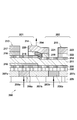
- FIG. 2 is a schematic structural explanatory view for explaining the structure of a semiconductor device having a CMOS circuit structure which is one of preferred embodiments of the present invention.
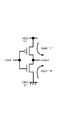
- FIG. 3 is a circuit diagram of the semiconductor device of FIG.
- FIG. 1 is a schematic structural explanatory diagram for explaining the structure of an nMOSTr which is one of the preferred embodiments of the present invention.
- the nMOSTr 100 of FIG. 1 shows n-type conduction characteristics, and a gate electrode 102, a gate insulating film 103, an active layer region 104 of an organic semiconductor (preferably pentacene), a source electrode region 105, and a drain electrode region 106 are formed on a substrate 101.
- the stacked structure is superposed in this order.
- the feature is that the layer region (A) including lanthanum boride (hereinafter also referred to as “LaB 6 ”) sandwiched between the active layer region 104 and the gate insulating film 103 in contact with the active layer region 104. 107 is provided.
- the layer region (A) 107 has a function of increasing the mobility of the active layer region 104 by supplying electrons to the active layer region 104 when the nMOS Tr 100 operates. That is, the layer region (A) 107 functions as an electron supply layer.
- Lanthanum boride (LaB 6 ) is a low work function material by itself, but the work function can be further reduced by adding nitrogen (N) during the manufacturing process of the active layer region 104.
- the nMOSTr 100 in FIG. 1 has the above-described structure as a basic structure, but if necessary, a first interface control layer is provided between the gate insulating film 103 and the layer region (A) 107 according to the purpose. 108 is provided. Furthermore, the source electrode portion 105 and the drain electrode portion 106 are provided with a second interface control layer 109 on the active layer region 104 side so as to be in direct contact with the active layer region 104.
- the interface control layer 108 is provided as necessary to improve the characteristics of the interface between the gate insulating film 103 and the active layer region 104 (particularly, to improve the generation of interface states).
- the interface control layers 108 and 109 are preferably made of a heat resistant material in consideration of the process temperature in the subsequent manufacturing process.
- a material polyvinylphenol (hereinafter sometimes abbreviated as “PVPh”) may be mentioned as a material suitably employed in the present invention.
- the threshold voltage can be stabilized by providing the interface control layer 108.
- the interface control layer 108 is formed by vapor deposition of PVPh, the layer thickness can be made extremely thin without pinholes, and the threshold voltage can be stabilized and the operating voltage can be greatly reduced.
- the interface control layer 109 is provided as necessary in order to improve the interface characteristics between the source electrode portion 105 / drain electrode portion 106 and the active layer region 104.
- the interface control layer 109 is composed of vapor deposition type PVPh, the interface state that causes carrier trapping can be greatly reduced. Therefore, in the present invention, the setting of the interface control layer 109 of PVPh is performed. Is a preferred embodiment.
- the interface control layer 109 is preferably made of a heat resistant material in consideration of the process temperature in the subsequent manufacturing process.
- a planarization region 110 (110a) is formed with a resin or the like so as to be flat with the upper surface 111 of the gate electrode 102. 110b).
- the planarization region 110 is made of a resin, it is desirable to use a heat-resistant resin so that high-temperature treatment can be easily applied in the subsequent process steps.
- various materials can be used as the substrate 101, but heat-resistant plastic, glass, metal, ceramics, etc. are preferably employed.
- examples of such materials include quartz, blue plate glass, alkali metal-less glass, silicon (silicon) substrate, metal substrate such as aluminum and stainless steel, semiconductor substrate such as gallium arsenide (GaAs), and thermoplastic or thermosetting.
- GaAs gallium arsenide
- thermoplastic or thermosetting A plastic substrate or the like is used. If heat resistance is not so required (process temperature 200 ° C.
- polyolefin such as polyethylene, polypropylene, ethylene-propylene copolymer, ethylene-vinyl acetate copolymer (EVA), cyclic polyolefin, modified Polyolefin, polyvinyl chloride, polyvinylidene chloride, polystyrene, polyamide, polyimide, polyamideimide, polycarbonate, poly- (4-methylbenten-1), ionomer, acrylic resin, polymethyl methacrylate, acrylic-styrene copolymer (AS Resin), butadiene-styrene copolymer, polio copolymer (EVOH), polyethylene terephthalate, polybutylene terephthalate, polyethylene naphthalate, precyclohexane terephthalate (PCT), etc.
- polyolefin such as polyethylene, polypropylene, ethylene-propylene copolymer, ethylene-vinyl acetate copolymer (EVA
- thermoplastic elastomers such as resin, styrene, polyolefin, polyvinyl chloride, polyurethane, fluoro rubber, chlorinated polyethylene, epoxy resin, phenol resin, urea resin, melamine resin, unsaturated polyester, silicone resin
- the plastic substrate material include polyurethane and the like, copolymers and blends mainly composed of these, and polymer alloys.
- stacked 2 or more types of the said material can also be used.
- the electrode material constituting the gate electrode 102 almost any material can be adopted as long as it is a material normally used in the semiconductor field.
- the substrate 101 is required to have a heat resistance of a certain level or more. Material selection is made.
- the electrode material constituting the gate electrode 102 is desirably selected from the following conductor materials.
- the following conductor materials For example, Cr, Al, Ta, Mo, Nb, Cu, Ag, Au (4.9 eV), Pt, Pd, In, Ni, Nd, Ca, Ti, Ta, Ir, Ru, W And metals such as Mo and Ru-Mo alloys and alloys of these metals.
- conductive oxides such as InO 2 , SnO 2 , ITO, conductive nitrides such as TiN and TaN, conductive polymers such as polyaniline, polypyrrole, polythiophene, or polyacetylene, graphene, carbon nanotubes, charge transfer complexes Molecular conductors such as those, and their laminated structure members.
- dopants such as acids such as hydrochloric acid, sulfuric acid, sulfonic acid, Lewis acids such as PF 6 , AsF 5 , FeCl 3 , halogen atoms such as iodine, and metal atoms such as sodium and potassium are added to the conductive polymer.
- a thing may be used.
- a conductive composite material in which carbon black or metal particles are dispersed may be used.
- the gate electrode 102 be formed as thin as possible within a range in which an electrode function is exhibited in consideration of flatness of a layer (or film) formed thereon and no pinhole is generated. Specifically, it is desirable that the film is formed with a thickness of usually 100 nm or less, preferably 50 nm or less, more preferably 10 nm or less.
- the planarization region 110 is preferably made of a heat-resistant material, but if the heat resistance is not required so much (process temperature of 200 ° C. or less), the material preferably selected as the material constituting the planarization region 110 The selection range is further expanded.
- a resin material having excellent coating properties is desirable.
- a resin most resins can be used as long as they are solvent-soluble among thermoplastic resins, thermosetting resins, and photocurable resins.
- PPS polyphenylene sulfide
- PAR polyarylate
- PAR polysulfone or polysulfone
- PES polyethersulfone
- PEI polyetherimide
- PAI polyamideimide
- PEEK polyetheretherketone
- LCP liquid crystal polyester
- PP polypropylene
- PVDC polyvinylidene chloride
- PET polyethylene terephthalate
- PC polycarbonate
- fluororesin PTFE
- melamine resin melamine resin
- PF phenol resin
- Examples thereof include an epoxy resin (EP), an unsaturated polyester resin (UP), and polyvinylphenol (PVPh).
- heat resistant temperature is more than 150 ° C
- resins with higher heat resistance include polyarylate (PAR), polysulfone (PSF), polyphenylene sulfide (PPS), polyetheretherketone (PEEK), A polyimide resin, a fluororesin, etc. are preferable.
- Polyamideimide (PAI), polyetheretherketone (PEEK) and the like are particularly preferable materials in the present invention because they have a heat resistance of 250 ° C. or more and can be used for a long time.
- polyvinylphenol (PVPh) that can form an ultra-thin film without pinholes is also a particularly preferable material in the present invention.
- the planarization region 110 is made of resin, and is made of an inorganic insulating material such as silicon oxide (SiO 2 ), silicon nitride (Si 3 N 4 ), silicon oxynitride (SiNO), or silicon carbonitride (SiCN). Also good.
- the gate insulating film 103 needs to be formed by selecting a material and a manufacturing process that can ensure gate capacitance and leakage current prevention.
- the gate insulating film 103 is preferably made of a heat-resistant material so that high-temperature processing can be performed in a process step applied after film formation. Examples of such materials include inorganic insulating materials such as silicon oxide (SiO 2 ), silicon nitride (Si 3 N 4 ), silicon oxynitride (SiNO), and silicon carbonitride (SiCN).
- the gate insulating film 103 should be selected from a material having a higher dielectric constant and excellent electrical matching with the adjacent layer (low interface state). It is desirable to form with an appropriate manufacturing process and manufacturing conditions. As such a material, there is a material called a so-called high-k material, and it is desirable to select and use the material according to the design requirements of the electronic device.
- high-k materials include oxides of transition metals such as HfO 2 and ZrO 2 from the viewpoint of leakage current, mobility, heat resistance, defects in the film and interface, impurity diffusion, and the like.
- Silicate HfSi x O y , ZrSi x O y
- Al 2 O 3 and their complex oxides Hf 1-x Al x O y , Zr 1-x Al x O y
- mixed oxides composed of various elements of Si, Hf, Ti and La, rutile type TiO 2 (relative permittivity about 80), (Ba, Sr) TiO 3 (perovskite), SrBi 4 Ti 4 O 15 , SrBi 2 Ta 2 O 9 , Ta 2 O 3 , La 2 O 3 , Dy 2 O 3 , rare earth oxides based on La 2 O 3 , HfSiON, and the like can also be used.
- the gate insulating film 103 may be formed of a laminated structure member having a structure in which a plurality of these materials are appropriately selected and each is laminated in a layered form.
- a laminated structure member for example, a two-layer structure such as HfSiON / SiO 2 , HfO 2 / Al 2 O 3 , TiO 2 / La 2 O 3 , HfLaSiO / SiO 2 , HfO 2 / Y 2 O 3 / al 2 O 3, TiO 2 / HfSiO / SiO 2, include a three-layer structure such as.
- the present invention is suitable for forming the gate insulating film 103. Material.
- the gate insulating film 103 is preferably a film made of an Hf-based material.
- the Hf-based high-k film can add La to shift the effective work function of the metal electrode to the low energy side.
- the addition amount of La and the distribution in the film thickness direction are important, it is desirable to form the film with sufficient consideration in this respect in the film design.
- increasing the amount of La added is promising because it is close to the La-based oxide and the relative dielectric constant is as high as about 27.
- the La-based oxide is hygroscopic and reacts with moisture in the atmosphere, it is vacuum. Therefore, it is necessary to consider the use of integrated production without breaking the process, or placing it in a rare gas atmosphere such as Ar or He in the process of forming an electronic device.
- the gate insulating film 103 for adding La, it is desirable to form the gate insulating film 103 by co-sputtering using an HfTi target and an HfLa target.
- the amount of La added may be adjusted by changing the composition ratio of La in the HfLa target as desired.
- the amount of La added in the gate insulating film 103 can be adjusted by intermittently shielding the HfLa target from the plasma.
- HfO 2 is a preferable material for forming the gate insulating film 103 because the dielectric constant can be significantly improved by adding yttrium (Y) and silicon (Si).
- the gate insulating film 103 a self-assembled monolayer (SAM) can be used.
- the gate insulating film 103 may be formed of the SAM itself or may have a multilayer structure of SAM.
- the multilayer structure film of SAM include a Langmuir film.
- it can be adopted as a film having a composite laminate structure of an Al 2 O 3 thin film and n-octadecylphosphonic acid SAM.
- a preferable combination of materials constituting the gate electrode 102 and the gate insulating film 103 can be appropriately selected from the materials described above.
- Mo / HfSiON / SiO 2 Metal / HfLaSiO / SiO 2 combinations such as Mo-O-Hf / HfSiON / SiO 2 , TiN / HfSiON combinations, Metal / HfSiO / TiO 2 combinations, TiN / TiO 2 / A combination of HfSiO and the like can be given.
- the interface characteristics between the gate electrode 102 and the gate insulating film 103 have a great influence on the device (semiconductor element) characteristics. Therefore, it is preferable to form the gate electrode 102 and the gate insulating film 103 by caution and contrivance more than selection of materials so as to suppress formation of an interface state for trapping carriers and formation of an energy barrier. .
- the gate electrode 102 and the gate insulating film 103 are formed in a consistent vacuum.
- the vacuum consistent interfacial solid phase reaction method is a solid phase interface reaction (SPIR) method based on physical vapor deposition (Physical Vapor Deposition) (H. Watanabe et al., Appl. , 449, 2004.).
- SPIR solid phase interface reaction
- the layer region (A) 107 is composed of lanthanum boride (LaB 6 : lanthanum hexaboride), and is preferably composed of nitrogen-containing lanthanum boride (LaB 6 (N)). Is desirable.
- a more preferable LaB 6 (N) film employed for the layer region (A) 107 has a crystal structure and contains 0.3 to 0.5 atomic% of nitrogen atoms, In the crystal, the proportion of crystals in the particle size range of 10 to 250 nm is 20 to 90%, and the crystallinity of the film is 20% or more. More preferable is a film in which the maximum peak of the crystal grain size distribution in the range of 10 to 250 nm is in the range of 15 to 150 nm.
- the inventors presume that by setting the above numerical range, not only a LaB 6 film having a low work function of 2.4 eV but also an interface affinity with the active layer region 104 is excellent. It seems that the film has good characteristics and good adhesion. Therefore, the desired adhesion is maintained even when the cumulative usage time of the device is considerably long, and a LaB 6 film excellent in resistance to change with time can be obtained without causing film floating or film peeling.
- the proportion of the crystals in the particle size range of 10 to 250 nm in all the crystals in the film is preferably in the above numerical range, more preferably 50 to 90%, still more preferably 80%. It is desirable to be ⁇ 90%. Even more preferably, the proportion of crystals in the particle size range of 30 to 200 nm is desirably 50 to 90%. Further, it is particularly desirable that the proportion of crystals in the particle size range of 50 to 150 nm is 50 to 90%.
- the crystallinity of the film is also important.
- the degree of crystallinity is preferably 20% or more as described above, more preferably 30% or more, and still more preferably 50% or more.
- the peak position of the crystal grain size distribution is also an important parameter for obtaining a more suitable LaB 6 (N) film of the present invention.
- the maximum of the grain size distribution peak in the range of 10 to 250 nm is desirably within 15 to 150 nm, more preferably 15 to 120 nm, and still more preferably 20 It is desirable to be in the range of ⁇ 100 nm.
- the source electrode portion 105 and the drain electrode portion 106 are made of a material appropriately selected in relation to the material constituting the active layer region 104 so that the contact with the active layer region 104 is electrically smooth. desirable. That is, in the case of the nMOSTr 100, since the active layer region 104 has n-type operating characteristics, the source electrode portion 105 is made of a material having a small work function. When the active layer region 104 is made of pentacene and has n-type operating characteristics, the material is appropriately selected so as to be as consistent as possible with pentacene LUMO (Lowest Unoccupied Molecular Orbital) 3.2 eV.
- LUMO Large Unoccupied Molecular Orbital
- the drain electrode portion 106 has the same material selection criteria. However, in the case of the drain electrode portion 106, electrons are easily released from the LUMO of the material constituting the active layer region 104 to the drain electrode portion 106.
- an organic semiconductor element having p-type operating characteristics is also used. Therefore, it is desirable that materials constituting the source electrode portion and the drain electrode portion in that case are appropriately selected from the following viewpoints. That is, when the active layer region 104 is made of an organic semiconductor material and has p-type operating characteristics, the organic semiconductor material HOMO (Highest Occupied Molecular Orbital) (5.0 eV in the case of pentacene) is matched as much as possible. The material is appropriately selected so that the properties can be obtained.
- HOMO Highest Occupied Molecular Orbital
- the source electrode portion 105 may have a stacked structure of, for example, an upper electrode region 105a made of an inexpensive and easy-to-handle material and a lower electrode region 105b made of a material having a small work function.
- the upper electrode region 105a is made of a metal such as Al or Cu
- the lower electrode region 105b is made of lanthanum boride or the like.
- the lower electrode region 105b is preferably composed of LaB 6 (N) having the characteristics described above.
- the upper electrode region 106a is made of Al and the lower electrode region 106b is made of Ni.
- the composite layer structure of the electrode parts 105 and 106 is preferable.
- a film forming method in the case of forming a film with an organic material, various film forming methods are adopted depending on the characteristics and application of the electronic element to be formed and the film forming material to be used.
- the film forming method that can be employed in the present invention include a coating method, a vacuum deposition method, CVD (Chemical Vapor Deposition), PCVD (Plasma Chemical Vapor Deposition), and the like.
- the coating method include spin coating, casting, and printing.
- the printing method include offset printing, letterpress printing, intaglio printing, gravure printing, screen printing, ink jet printing, and micro contact printing.
- ink jet printing or micro contact printing In the case of fineness of 10 ⁇ m or less, it is preferable to employ ink jet printing or micro contact printing.
- ink jet printing or micro contact printing In particular, in an organic TFT, it is known that the switching characteristics of the element are improved by reducing the distance between the source electrode and the drain electrode (channel length: L). It is desirable to employ microcontact printing that allows area patterning.
- the present invention is not limited to this, and any electronic device can be used as long as the electron supply layer provided in direct contact with the active layer region is lanthanum boride. Applies to For example, it can be applied to a top gate type nMOSTr.
- Al gate electrode is formed on a plastic or glass substrate (deposition method, 10 ⁇ 6 Pa).
- a transparent heat-resistant plastic film is formed (coating method, heat treatment at 250 ° C.).
- High dielectric constant nitride film HfNx (relative dielectric constant 26) 10 nm is formed (sputtering method, 0.2 Pa).
- FIG. 2 is a schematic structural explanatory diagram for explaining the structure of a semiconductor device having a CMOS circuit structure which is one of preferred embodiments of the present invention.
- FIG. 3 is a circuit diagram of the semiconductor device of FIG.
- the CMOS semiconductor device 200 includes nMOSTr 201 and pMOSTr 202.
- the nMOSTr 201 has the same configuration as that of the nMOSTr 100 shown in FIG.
- the CMOS semiconductor device 200 has input terminals 203 a and 203 b and an output terminal 204. As shown in FIG. 3, the input terminals 203a and 203b are connected on the input upstream side.
- the nMOSTr 201 operates when an “L” level signal is input
- the pMOSTr 202 operates when an “H” level signal is input.
- the first common interface control layer 209 and the second common interface control layer 212 are provided in a more preferred embodiment example, and the interface with the common active layer region 211 has sufficient characteristics in device design. If there is, it is not necessarily provided.
- the electron supply layer region 210 is provided only on the nMOSTr 201 side as shown in the drawing, and supplies electrons to a portion of the active layer region on the nMOSTr 201 side of the common active layer region 211.
- the electron supply layer region 210 is the same as the layer region (A) 107 and is formed by the same material and manufacturing method as described in the layer region (A) 107.
- Flattened regions 207a, 207b, and 207c are provided on both sides of the gate electrodes 206a and 206b as in the case of FIG.
- the source electrode portion 213 is essentially the same as the source electrode portion 105 shown in FIG. 1, the upper electrode region 217 is essentially the same as the upper electrode region 105a, and the lower electrode region 216 is essentially the same as the lower electrode region 105b. .
- the source electrode portion 215 is essentially the same as the drain electrode portion 106 shown in FIG. 1, the upper electrode region 223 is essentially the same as the upper electrode region 106a, and the lower electrode region 222 is essentially the same as the lower electrode region 106b. .
- the drain electrode portion 214 is provided with a structure in which the drain electrode portion of the nMOSTr 201 and the drain electrode portion of the pMOSTr 202 are partially separated. That is, the lower electrode region 218 of the drain electrode portion of the nMOSTr 201 and the lower electrode region 219 of the drain electrode portion of the pMOSTr 202 are electrically separated by the separation region 220.
- the lower electrode region 218 is made of Ni, for example, like the lower electrode region 106b.
- the lower electrode region 219 is made of a low work function material, for example, lanthanum boride, like the lower electrode region 105b. In particular, it is desirable to use LaB 6 (N) having the characteristics described above.
- the upper electrode region 221 is made of, for example, a metal such as Al.
- the common active layer region 211 is the same as the active layer region 104, and is formed by the same material and manufacturing method as described in the active layer region 104.
- the substrate 205 is the same as the substrate 101.
- the gate insulating film 208 is the same as the gate insulating film 103.
- the gate electrodes 206a and 206b are the same as the gate electrode 102.
- the first common interface control layer 209 and the second common interface control layer 212 are the same as the first interface control layer 108 and the second interface control layer 109, respectively.
- Al gate electrode 1 ⁇ m Al gate electrode is formed on a plastic or glass substrate (deposition method, 10 ⁇ 6 Pa).
- B2 A transparent heat-resistant plastic film is formed (coating method, heat treatment at 250 ° C.).
- B3) High dielectric constant nitride film HfNx (relative dielectric constant 26) 10 nm is formed (sputtering method, 0.2 Pa).
- B4) Forming 2-3 nm of polyvinylphenol (PVPh) as an ultra-thin interface control layer (deposition method, 10 ⁇ 4 Pa).
- NiB added (0.4%) LaB 6 is formed to 1 nm in the nMOSTr region (sputtering method, 1 Pa).
- PVP (2 nm) / pentacene (20 nm) is formed in the nMOSTr and pMOSTr regions (evaporation method, 10 ⁇ 4 Pa).
- Au (5.2 eV) and Ni (5.2 eV) are formed to a thickness of 20 nm as a source of pMOSTr and a drain of nMOSTr (deposition method, 10 ⁇ 6 Pa).
- Nitrogen-added LaB 6 is formed to a thickness of 20 nm as a drain of pMOSTr and a source of nMOSTr (deposition method, 1 Pa).
- a 20-nm PVP thin film was formed between the drain electrodes of pMOSTr and nMOSTr (evaporation method, 10 ⁇ 4 Pa).
- Al electrode is formed with a thickness of 1 ⁇ m (evaporation method, 10 ⁇ 6 Pa).
- Al between source / drain electrodes is dry-etched (chlorine gas).
Landscapes
- Chemical & Material Sciences (AREA)
- Inorganic Chemistry (AREA)
- Thin Film Transistor (AREA)
- Electroluminescent Light Sources (AREA)
- Metal-Oxide And Bipolar Metal-Oxide Semiconductor Integrated Circuits (AREA)
Abstract
有機半導体素子は、ソース電極部105と、ドレイン電極部106と、有機半導体の活性層領域104と、ゲート絶縁膜103と、ゲート電極部102と、前記活性層領域に接して前記ゲート絶縁膜側に硼化ランタンを含む層領域107とを有している。
Description
本発明は、有機半導体素子及びそれを備えたCMIS半導体装置に関するものである。
有機半導体は、一般にシリコン単結晶半導体に比べ、キャリア移動度の点を除けば、可撓性、軽量性、耐衝撃性、薄型性、低コスト性、大面積性に於いて優位性を有している。特に、面積コストにおいては、面積が大きくなればなるほどその優位性は顕著になる。その為、自発光表示装置、太陽電池などの大面積エレクトロニクスデバイスに向くので産業界の期待は大きい。
しかし、一方、有機半導体には、それなりのホール移動度を有するものもあるが、大概は単結晶のものであり、有機半導体の特徴である大面積化(大面積に亘って多数の薄膜トランジスタ(以後「Thin Film Transistor:TFT」と記すこともある)を活かしきれない状況にある。
しかも、有機半導体の場合は、n型半導体・p型半導体という材料ではなく其の殆どが真正(i型)半導体若しくはそれに近いものである。即ち、有機半導体の場合は、シリコン(Si)のような一般的な無機半導体のように不純物を添加(ドーピング)して半導体そのものをn型・p型にしてn型半導体動作・p型半導体動作をさせるものではなく、電極/有機半導体の界面及び絶縁体/有機半導体の界面を制御することによりn型動作・p型動作をさせるようにしているのが実情である。その理由は、無機半導体のように効率よくドーピングして実用に耐えるn型・p型の有機半導体がまだ実現されていないことにある。
有機半導体をn型動作・p型動作させるには、次のようなことが考えられ研究レベルでは一部実現している。即ち、p型動作させるためには、選択した有機半導体材料のHOMO(Highest Occupied Molecular Orbital)と出来るだけ整合するように仕事関数の大きな材料で電極を構成し、該有機半導体材料のHOMOへの正孔注入をしやすくする。n型動作させるためには、選択した有機半導体材料のLUMO(Lowest Unoccupied Molecular Orbital)と出来るだけ整合するように仕事関数の小さな材料で電極を構成し、該有機半導体材料のLUMOへの電子注入をしやすくする。
しかし、大面積化に向く薄膜状(非晶質若しくは多結晶、微結晶)のものとなると、一般に、伝導特性がp型動作のものに比べ、n型動作のものには実用に十分供される移動度(移動度そのものを大きくするのではなく、電極より注入されるキャリア濃度を十分とすることで、キャリア蓄積層にキャリアを十分に蓄積することで、移動度を見掛け上大きくする)を安定的に有するものがないのが実情である。況してや、電子移動度とホール移動度が実用に供される値を有する両極性の材料となると皆無である。そのため、CMOS回路構成に代表されるCMIS回路構成の半導体装置を作成するとなると、p型とn型で材料を別々に選択しなければならず、製造プロセスの煩雑さに加え工数増を招き生産の効率低下とコスト向上という不都合が生ずる。
その中でも、両極性有機半導体材料の一つであるペンタセンは、有望視されている材料の一つである。しかし、そのキャリア移動度が、ホールの場合は、アモルファスシリコン(以後「A-Si」と略記することもある)並みの0.1~1cm2/Vsec程度が得られているのに対し、電子の場合は、精々0.05cm2/Vsec程度と極めて小さい。そのために、消費電力の点で優れているCMOS半導体装置へ適用しようとすると、pMOSトランジスタ(以後「pMOSTr」と記すこともある)とnMOSトランジスタ(以後「nMOSTr」と記すこともある)との間で特性上の極端な不整合性が生じ、有機半導体の優位性を十分活かしきれていない。
この課題を解決するために、ペンタセンからなる活性層領域とゲート絶縁膜の界面に、電子供給層としてCa(カルシウム)(2.8eV)などの仕事関数の小さい金属層を導入して見掛け上の電子の移動度を向上させる(実際は、活性領域をソース側からドレイン側に流れる電流を増大させる)ことで、ペンタセンのn型動作特性の改善を図るという報告がある(非特許文献1)。
Japanese Journal of Applied Physics 51 (2012) 04DK01.
しかし、Caなどの金属は酸化しやすく、デバイス動作特性及びデバイス製造の生産効率・量産性に課題が存在している。特にカルシウム(Ca)は、空気中で放置すると酸素・水・二酸化炭素と反応して腐食する、殊に水とは激しく反応して水素を発生する、また、ハロゲンとは気相中で直接反応し、ハロゲン化物を生成する、など化学反応性に富むため生産ラインでの取り扱いも煩雑になる傾向にある。
本発明は上記点に鑑み鋭意研究することによりなされたものであって、その目的は、有機半導体素子のn型動作特性の改善を図ることにある。
本発明のもう一つの目的は、ペンタセンのn型動作特性の改善を図り、ペンタセンを使用するp型動作電子素子と同等以上のn型動作特性を有する有機半導体素子並びにその素子を構成電子素子として備えたCMIS回路構成、特にCMOS回路構成を有する半導体装置を提供することである。
本発明の一つの側面は、ソース電極部、ドレイン電極部、有機半導体の活性層領域、ゲート絶縁膜、ゲート電極部、を備えた有機半導体素子に於いて、前記有機半導体はペンタセンであり、前記活性層領域に接して前記ゲート絶縁膜側に硼化ランタン(以後「LaB6」と記すこともある)を含む層領域(A)を設けたことを特徴とする有機半導体素子にある(第一の発明)。
本発明のもう一つの側面は、上記第一の発明に於いて、前記層領域が窒素を含むことを特徴とする有機半導体素子にある(第二の発明)。
本発明の別の側面は、前記第一の発明に於いて、前記ソース電極部は、前記活性層領域に電気的に直接接続している硼化ランタンを含む層領域(A)を備えていることを特徴とする有機半導体素子にある(第三の発明)。
本発明の別の側面は、ソース電極部、ドレイン電極部、ペンタセンの活性層領域、該活性層領域に直接接している、窒素含有硼化ランタン(以後「LaB6(N)」と記すこともある)を含む層領域(A)、ゲート絶縁膜、ゲート電極部、を備えていることを特徴とする有機半導体素子にある(第四の発明)。
本発明の更に別の側面は、前記第一の発明乃至前記第四の発明の中から選択される有機半導体素子であって、前記活性層領域は、ポリビニルフェノールで構成された第一の層と第二の層とに挟持されていることを特徴とする有機半導体素子にある(第五の発明)。
本発明のもう一つの側面は、ソース電極部、ドレイン電極部、有機半導体の活性層領域、ゲート絶縁膜、ゲート電極部、を備えた有機半導体素子に於いて、前記活性層領域に接して、前記ゲート絶縁膜側に、前記活性層領域に電子を供給するための硼化ランタンを含む層領域(A)が設けてあることを特徴とするn型動作特性を示す有機半導体素子にある(第六の発明)。
本発明の更に別の側面は、CMIS回路構成を備えたCMIS半導体装置において、前記CMIS回路を構成するn型動作の電子素子が、前記第一の発明乃至前記第六の発明の中から選択される有機半導体素子であることを特徴とするCMIS半導体装置にある(第七の発明)。
本発明のもう一つ別の側面は、ソース電極部、ドレイン電極部、有機半導体の活性層領域、ゲート絶縁膜、ゲート電極部、を備えた有機半導体素子に於いて、前記ドレイン電極部の前記活性層領域側の少なくとも一部に硼化ランタンを含む層領域が設けてあることを特徴とするp型動作特性を示す有機半導体素子にある(第八の発明)。
本発明によれば、デバイス動作特性が高く動作安定性に優れ、デバイス製造の生産効率が高く量産に向いた有機半導体素子及びCMIS半導体装置が得られる。又、本発明によれば、高速で低電圧駆動できる有機半導体素子及びCMIS半導体装置が得られる。
本発明のその他の特徴及び利点は、添付図面を参照とした以下の説明により明らかになるであろう。なお、添付図面においては、同じ若しくは同様の構成には、同じ参照番号を付す。
添付図面は明細書に含まれ、その一部を構成し、本発明の実施の形態を示し、その記述と共に本発明の原理を説明するために用いられる。
図1は、本発明の好適な実施態様例の一つであるnMOSTrの構造を説明するための模式的構造説明図である。
図2は、本発明の好適な実施態様例の一つであるCMOS回路構造を備えた半導体装置の構造を説明するための模式的構造説明図である。
図3は、図2の半導体装置の回路図である。
図1は、本発明の好適な実施態様例の一つであるnMOSTrの構造を説明するための模式的構造説明図である。
図1のnMOSTr100は、n型伝導特性を示し、基体101上に、ゲート電極102、ゲート絶縁膜103、有機半導体(好ましくはペンタセン)の活性層領域104、ソース電極領域105、ドレイン電極領域106が、この順で重畳された積層構造を有する。そして、その特徴は、前記活性層領域104に接して該活性層領域104とゲート絶縁膜103に挟持され、硼化ランタン(以後「LaB6」と記すこともある)を含む層領域(A)107が設けられた構造を有していることである。
前記層領域(A)107は、前記nMOSTr100が動作する際、前記活性層領域104に電子を供給して前記活性層領域104の移動度を高める機能を有する。即ち、層領域(A)107は、電子供給層として機能する。硼化ランタン(LaB6)は、それだけでも低仕事関数の材料であるが、前記活性層領域104の製造プロセス過程で窒素(N)を添加することで仕事関数をより小さくすることができる。
図1のnMOSTr100は、上記の構造が基本構造であるが、更に必要であれば、その目的に応じて、ゲート絶縁膜103と層領域(A)107の間には、第一の界面制御層108が設けられる。更には、ソース電極部105・ドレイン電極部106には、活性層領域104側に、該活性層領域104に直接接して第二の界面制御層109が設けられる。界面制御層108は、ゲート絶縁膜103と活性層領域104との界面の特性向上(特に界面準位の発生抑制の向上)のために必要に応じて設けられる。
界面制御層108、109は、その後の製造プロセスにおけるプロセス温度を考慮して耐熱性の材料で構成するのが望ましい。その様な材料として、本発明に於いて好適に採用される材料には、ポリビニルフェノール(以後、「PVPh」と略記することもある)が挙げられる。
ゲート絶縁膜103と活性層領域104との界面の特性は、特にnMOSTr100の閾値電圧の安定化に影響を及ぼすが、界面制御層108を設けることで閾値電圧の安定化を図ることが出来る。特に、界面制御層108を、PVPhの蒸着によって形成すれば、その層厚をピンホールなく極薄化することができ、閾値電圧の安定化と動作電圧の低減化を大幅に図ることが出来る。
また、界面制御層109は、ソース電極部105・ドレイン電極部106と活性層領域104との間の界面特性を改善するために必要に応じて設けられる。特に、界面制御層109を蒸着系のPVPhで構成することで、キャリアトラップの元になる界面準位を大いに低減させることが出来るので、本発明に於いては、PVPhの界面制御層109の設定は好ましい態様である。界面制御層109についても、界面制御層108と同様、その後の製造プロセスにおけるプロセス温度を考慮して耐熱性の材料で構成するのが望ましい。
基体101上に設けたゲート電極102の周囲には、ゲート電極102上にゲート絶縁膜103を設けるために、ゲート電極102の上面111と平坦にするために、樹脂などで平坦化領域110(110a、110b)が設けられる。平坦化領域110を樹脂で構成する場合は、その後のプロセス工程で高温処理が適用され易くするために耐熱性樹脂を用いるのが望ましい。
本発明に於いて基体101としては、様々な材料を用いることが可能であるが、好ましく採用されるのは、耐熱プラスチック、ガラス、金属、セラミックスなどである。その様な材料としては、例えば、石英、青板ガラス、アルカリ金属レスガラス、シリコン(ケイ素)基板、アルミニウム、ステンレス等の金属基板、ガリウムヒ素(GaAs)等の半導体基板、及び熱可塑性又は熱硬化性のプラスチック基板等が用いられる。また、耐熱性がそれ程要求されない(プロセス温度200℃以下)のであれば、例えば、ポリエチレン、ポリプロピレン、エチレン-プロピレン共重合体、エチレン-酢酸ビニル共重合体(EVA)等のポリオレフィン、環状ポリオレフィン、変性ポリオレフィン、ポリ塩化ビニル、ポリ塩化ビニリデン、ポリスチレン、ポリアミド、ポリイミド、ポリアミドイミド、ポリカーボネート、ポリ-(4-メチルベンテン-1)、アイオノマー、アクリル系樹脂、ポリメチルメタクリレート、アクリル-スチレン共重合体(AS樹脂)、ブタジエン-スチレン共重合体、ポリオ共重合体(EVOH)、ポリエチレンテレフタレート、ポリブチレンテレフタレート、ポリエチレンナフタレート、プリシクロヘキサンテレフタレート(PCT)等のポリエステル、ポリエーテル、ポリエーテルケトン、ポリエーテルエーテルケトン、ポリエーテルイミド、ポリアセタール、ポリフェニレンオキシド、変形ポリフェニレンオキシド、ポリアリレート、芳香族ポリエステル(液晶ポリマー)、ポリテトラフルオロエチレン、ポリフッ化ビニリデン、その他フッ素系樹脂、スチレン系、ポリオレフィン系、ポリ塩化ビニル系、ポリウレタン系、フッ素ゴム系、塩素化ポリエチレン系等の各種熱可塑性エラストマー、エポキシ樹脂、フェノール樹脂、ユリア樹脂、メラミン樹脂、不飽和ポリエステル、シリコーン樹脂、ポリウレタン等、またはこれらを主とする共重合体やブレンド体、ポリマーアロイ等がプラスチック基板の材料として挙げられる。また、上記材料のうちの2種以上を積層した複合積層体とした基体も用いることができる。
ゲート電極102を構成する電極材料としては、半導体分野で通常に使用されている材料であれば、大概の材料が採用され得る。
図1に示すようなボトムゲートタイプの電界効果トランジスタ(以後「FET」と記す場合もある)の場合は、基体101はある程度以上の耐熱性を要求されるので、設計上の所望の耐熱性に従って材料の選択がなされる。
本発明に於いてゲート電極102を構成する電極材料として望ましくは、以下の導電体材料から選択されるのが好ましい。その導電体材料としては、例えば、Cr、Al、Ta、Mo、Nb、Cu、Ag、Au(4.9eV)、Pt、Pd、In、Ni、Nd、Ca、Ti、Ta、Ir、Ru、W、Mo、Ru-Mo合金などの金属及びこれら金属の合金が挙げられる。その他、InO2、SnO2、ITO等の導電性の酸化物、TiN、TaNなどの導電性窒化物、ポリアニリン、ポリピロール、ポリチオフェン、またはポリアセチレン等の導電性高分子、グラフェン、カーボンナノチューブ、電荷移動錯体などの分子性導体、それらの積層構造部材が挙げられる。また、上記導電性高分子に塩酸、硫酸、スルホン酸等の酸、PF6、AsF5、FeCl3等のルイス酸、ヨウ素等のハロゲン原子、ナトリウムやカリウム等の金属原子等のドーパントを添加したものを用いてもよい。更に、カーボンブラックまたは金属粒子を分散した導電性の複合材料を用いてもよい。
ゲート電極102は、その上に形成される層(又は膜)の平坦性を考慮して電極機能が発揮され、ピンホールが発生しない範囲に於いて出来る限り薄く形成されるのが望ましい。具体的には、通常は100nm以下、好ましくは、50nm以下、より好ましくは、10nm以下の厚さで形成されるのが望ましい。
平坦化領域110は、好ましくは、耐熱材料で構成するのが望ましいが、耐熱性がそれ程要求されない(プロセス温度200℃以下)のであれば、平坦化領域110を構成する材料として好ましく選択される材料の選択範囲は、一段と拡大される。
平坦化領域110を構成する材料としては、好ましくは、塗膜性に優れた樹脂材料が望ましい。そのような樹脂としては、熱可塑性樹脂、熱硬化性樹脂、光硬化性樹脂の中で溶媒可溶性であれば大概の樹脂が使用できる。具体的には、ポリフェニレンスルフィド(PPS)、ポリアリレート(PAR)、ポリサルフォン又はポリスルホン(PSF)、ポリエーテルサルフォン(PES)、ポリエーテルイミド(PEI)、ポリアミドイミド(PAI)、ポリエーテルエーテルケトン(PEEK)、液晶ポリエステル(LCP)、ポリプロピレン(PP)、ポリ塩化ビニリデン(PVDC)、ポリエチレンテレフタレート(PET)、ポリカーボネート(PC)、フッ素樹脂(PTFE)、メラミン樹脂(MF)、フェノール樹脂(PF)、エポキシ樹脂(EP)、不飽和ポリエステル樹脂(UP)、ポリビニルフェノール(PVPh)等が挙げられる。これらの樹脂の中で、耐熱温度が150℃以上もあり、より高い耐熱性をもつ樹脂として、ポリアリレート(PAR)、ポリスルホン(PSF)、ポリフェニレンスルフィド(PPS)、ポリエーテルエーテルケトン(PEEK)、ポリイミド樹脂、フッ素樹脂などが好ましい。ポリアミドイミド(PAI)、ポリエーテルエーテルケトン(PEEK)などは、250℃以上の耐熱性があり、しかも長時間の使用も可能であるので、本発明に於いては、特に好ましい材料である。この他、ピンホールなく超極薄化膜の形成ができるポリビニルフェノール(PVPh)も、本発明に於いて特に好ましい材料である。平坦化領域110は樹脂で構成される他、酸化シリコン(SiO2)、窒化シリコン(Si3N4)、酸窒化シリコン(SiNO)、炭窒化シリコン(SiCN)などの無機絶縁材料で構成しても良い。
ゲート絶縁膜103は、ゲート容量とリーク電流防止を担保できる材料と製造プロセスが選択されて形成される必要がある。また、ゲート絶縁膜103は、成膜後に適用されるプロセス工程で高温処理が出来るように望ましくは耐熱性の材料で構成するのが好ましい。その様なものとしては、例えば、酸化シリコン(SiO2)、窒化シリコン(Si3N4)、酸窒化シリコン(SiNO)、炭窒化シリコン(SiCN)などの無機絶縁材料が挙げられる。
電子素子のより微細化・高性能化を実現するためには、ゲート絶縁膜103は、より高誘電率で隣接層との電気的整合性(低界面準位)に優れた材料を選択して適切な製造プロセスと製造条件で形成するのが望ましい。そのような材料としては、所謂、high-k材料として呼ばれている材料があり、その中から電子素子の設計上の所望に応じて選択して使用するのが望ましい。その様なhigh-k材料としては、リーク電流、移動度、耐熱性、膜中や界面に於ける欠陥、不純物拡散などの観点から、HfO2やZrO2などの遷移金属の酸化物、及びそれらのシリケート(HfSixOy、ZrSixOy)、Al2O3やそれらの複合酸化物(Hf1-xAlxOy、Zr1-xAlxOy)などが挙げられる。これらの他には、Si、Hf、Ti、Laの多種元素からなる混合酸化物、ルチル型TiO2(比誘電率約80)、(Ba、Sr)TiO3(ペロブスカイト)、SrBi4Ti4O15、SrBi2Ta2O9、Ta2O3、La2O3、Dy2O3、La2O3をベースにした希土類酸化物、HfSiON、なども使用し得る。
また、これらの材料の中から複数を適宜選択して夫々を層状にして積層(スタック)した構造の積層構造部材でゲート絶縁膜103を構成しても良い。そのよう積層構造部材としては、例えば、HfSiON/SiO2、HfO2/Al2O3、TiO2/La2O3、HfLaSiO/SiO2、などの2層構造、HfO2/Y2O3/Al2O3、TiO2/HfSiO/SiO2、などの3層構造のものが挙げられる。
上記に挙げた材料の大半は、EOT(Equivalent Oxide Thickness:酸化膜換算膜厚)1nm以下においてリーク電流を大幅に低減することができるので、本発明において、ゲート絶縁膜103を構成するのに好適な材料である。
本発明においては、その中でも、ゲート絶縁膜103としては、Hf系の材料で構成する膜が好ましい。Hf系high-k膜は、Laを添加してメタル電極の実効仕事関数を低エネルギー側にシフトさせることが出来る。この方法は、Laの添加量と膜厚方向の分布が重要であるので、膜設計においてはこの点を十分配慮して膜形成するのが望ましい。
また、Laの添加量を多くするとLa系酸化物に近き比誘電率が約27と高くなるので有望となるが、La系酸化物は吸湿性がるため大気中の水分と反応するので、真空を破ることなく一貫生産を採用するなり、あるいは電子素子形成過程では、Ar、Heなどの希ガス雰囲気中に置くなどの配慮が必要である。
また、Laの添加量を多くするとLa系酸化物に近き比誘電率が約27と高くなるので有望となるが、La系酸化物は吸湿性がるため大気中の水分と反応するので、真空を破ることなく一貫生産を採用するなり、あるいは電子素子形成過程では、Ar、Heなどの希ガス雰囲気中に置くなどの配慮が必要である。
また、Laの添加には、HfTiターゲットとHfLaターゲットを使用してCo-sputterすることで、ゲート絶縁膜103を形成するのが望ましい。その際のLaの添加量の調節は、HfLaターゲト中のLaの組成比を所望に従って変えれば良い。また、HfLaターゲットをプラズマから断続的に遮蔽したりして成膜することでゲート絶縁膜103中の、Laの添加量を調整することが出来る。
HfO2は、イットリウム(Y)、シリコン(Si)を添加することで誘電率を大幅に改善できるので、ゲート絶縁膜103を形成するには好ましい材料である。
ゲート絶縁膜103に、自己組織化単分子膜(Self-Assembled Monolayer:SAM)を採用することも出来る。その場合、ゲート絶縁膜103をSAMそのもので構成しても良いし、SAMの多層構造としても良い。SAMの多層構造膜としては、例えば、Langmuir膜なども挙げられる。或いは、例えば、Al2O3薄膜とn-オクタデシルホスホン酸のSAMの複合積層構造の膜として採用することも出来る。
本発明において、ゲート電極102とゲート絶縁膜103を構成する好ましい材料の組み合わせは、前述した材料の中から適宜選択することが出来る。譬えば、Mo/HfSiON/SiO2、Mo-O-Hf/HfSiON/SiO2などのMetal/HfLaSiO/SiO2の組合せ、TiN/HfSiONの組合せ、Metal/HfSiO/TiO2の組合せ、TiN/TiO2/HfSiOの組合せ、などが挙げられる。
ゲート電極102とゲート絶縁膜103の界面特性は、デバイス(半導体素子)特性に影響大である。従って、キャリアをトラップする界面準位の形成やエネルギー障壁の形成が抑制されるように、ゲート電極102とゲート絶縁膜103の形成には材料の選択以上の注意と工夫により製膜するのが好ましい。例えば、好ましくは、ゲート電極102とゲート絶縁膜103を真空一貫形成するのは望ましい。更に、例えば、TiN/HfSiOのような場合には、真空一貫界面固相反応法で形成するのも好ましい。真空一貫界面固相反応法は、物理蒸着(Physical Vapor Deposition)をベースとした界面固相反応(Solid Phase Interface Reaction:SPIR)法である(H.Watanabe et al., Appl. Phys. Lett. 85, 449, 2004.参照)。
層領域(A)107は、前述したように、硼化ランタン(LaB6:六硼化ランタン)で構成されるが、好ましくは、窒素含有硼化ランタン(LaB6(N))で構成するのが望ましい。
本発明において、層領域(A)107に採用されるより好ましいLaB6(N)膜は、結晶構造を有すると共に窒素原子を0.3~0.5原子%含み、且つ、該膜中における全結晶中の10~250nmの粒径範囲にある結晶の割合が20~90%であって、該膜の結晶化度が20%以上である膜である。更に好ましいのは、粒径が10~250nmの範囲における結晶粒径分布のピークの最大が、15~150nmの範囲にある膜である。
本発明者等が推測するには、上記の数値範囲とすることで、2.4eVという低仕事関数のLaB6膜とすることだけでなく、活性層領域104との界面親和性に優れるため界面特性が良好で、且つ密着性も良い膜になるものと思われる。そのため、デバイスの累積使用時間がかなり長時間になっても所期の密着性が維持され、膜の浮きや膜剥がれを起こさず経時変化対抗特性に優れたLaB6膜が得られる。
膜中における全結晶中の10~250nmの粒径範囲にある結晶の割合は、好ましくは、上記の数値範囲であるのが望ましいが、より好ましくは、50~90%、更により好ましくは、80~90%であるのが望ましい。より一層好ましくは、30~200nmの粒径範囲にある結晶の割合が50~90%であるのが望ましい。更には、50~150nmの粒径範囲にある結晶の割合が50~90%であるのが格段に望ましいものである。
本発明において、より良好な窒素含有六硼化ランタン(LaB6(N))膜を得るには、膜の結晶化度も重要である。結晶化度としては、好ましくは、上記した様に20%以上であるのが望ましいが、より好ましくは30%以上、更により好ましくは、50%以上であるのが望ましい。
結晶粒径分布のピーク位置も本発明のより好適なLaB6(N)膜を得るには重要なパラメーターである。本発明に於いては、粒径が10~250nmの範囲における結晶粒径分布のピークの最大が、15~150nm内にあるのが望ましく、より好ましくは、15~120nm、より一層好ましくは、20~100nmの範囲にあるのが望ましい。
ソース電極部105とドレイン電極部106は、活性層領域104とのコンタクトが電気的にスムーズになるように活性層領域104を構成する材料との関係において適宜選択される材料で構成されるのが望ましい。即ち、nMOSTr100の場合、活性層領域104はn型動作特性とされるため、ソース電極部105は、仕事関数の小さな材料で構成される。活性層領域104をペンタセンで構成しn型動作特性とする場合は、ペンタセンのLUMO(Lowest Unoccupied Molecular Orbital)3.2eVとできる限り整合性が取れるように材料の選択が適宜される。その結果、ソース電極部105から活性層領域104を構成する材料のLUMOへの電子の注入をしやすくする。ドレイン電極部106も材料の選択基準は同様であるが、ドレイン電極部106の場合は、活性層領域104を構成する材料のLUMOからドレイン電極部106への電子の放出をしやすくする。
後述するCMOS半導体装置の場合は、p型動作特性の有機半導体素子も使用されるので、その場合のソース電極部とドレイン電極部を構成する材料は以下の視点で適宜選択されるのが望ましい。即ち、活性層領域104を有機半導体材料で構成しp型動作特性とする場合は、該有機半導体材料のHOMO(Highest Occupied Molecular Orbital)(ペンタセンの場合は、5.0eV)とできる限りエネルギーレベルの整合性が取れるように材料の選択が適宜される。
図1に示すnMOSTr100の場合、ソース電極部105は、例えば、安価で取り扱い易い材料で構成した上部電極領域105aと仕事関数の小さな材料で構成した下部電極領域105bとの積層構造としても良い。例えば、上部電極領域105aは、Al、Cuなどの金属で、下部電極領域105bは、硼化ランタンなどで構成される。特に、下部電極領域105bは、好ましくは、前述した特性のLaB6(N)で構成するのが望ましい。ドレイン電極部106は、例えば、上部電極領域106aをAlで、下部電極領域106bをNiで構成される。この様に電極部105,106を複合層構造とすることにより、電極材料の選択範囲を広げられるので電極部105,106の複合層構造は好ましい。
本発明に於いて、有機材料で製膜する場合の製膜法には、形成する電子素子の特性や用途、採用する成膜材料に応じて種々の製膜法が採用される。本発明に於いて採用され得る製膜法には、塗布法、真空蒸着法、CVD(Chemical Vapor Deposition)、PCVD(Plasma Chemical Vapor Deposition)などが挙げられる。塗布法としては、スピンコート法、キャスト法、印刷法などが挙げられる。印刷法としては、オフセット印刷、凸版印刷、凹版印刷、グラビア印刷、スクリーン印刷、インクジェットプリント、マイクロコンタクトプリントなどが挙げられる。精細度において、10μm以下の場合は、インクジェットプリント、マイクロコンタクトプリントを採用するのが好ましい。特に、有機TFTにおいては、ソース電極とドレイン電極の間隔(チャネル長:L)を小さくすることで、素子のスイッチング特性が良くなることが知られているので、好ましくは、サブμmオーダーでの大面積パターニングも可能なマイクロコンタクトプリントの採用が望ましい。
図1では、ボトムゲートタイプのnMOSTrで説明したが、本発明はこれに限定されるものではなく、活性層領域に直接接して設けられた電子供給層が硼化ランタンであればすべての電子素子に適用される。例えば、トップゲートタイプのnMOSTrにも適用出来る。
以下に、図1に示すnMOSTrの作製の工程と作成条件の好適な例の一つの概略を示す。
(A1)プラスチックやガラス基板上にAlゲート電極を1μm形成(蒸着法、10-6Pa)。
(A2)透明耐熱性プラスチック膜を形成(塗布法、250℃で熱処理)。
(A3)高誘電率窒化膜HfNx(比誘電率26)10nmを形成(スパッタ法、0.2Pa)。
(A4)極薄界面制御層としてポリビニルフェノール(PVPh)を2~3nm形成(蒸着法、10-4Pa)。
(A5)窒素添加(0.4%)LaB6を1nm形成(スパッタ法、1Pa)。
(A6)PVP(2nm)/ペンタセン(20nm)を形成(蒸着法、10-4Pa)。
(A7)ドレイン電極部としてAu(5.2eV)、Ni(5.2eV)を20nm形成(蒸着法、10-6Pa)。
(A8)ソースとして窒素添加LaB6を20nm形成(蒸着法、1Pa)。
(A9)Al電極を1μm形成(蒸着法、10-6Pa)。
図2には、本発明の好適な実施態様例の一つであるCMOS回路構造を備えた半導体装置の構造を説明するための模式的構造説明図が示される。図3は、図2の半導体装置の回路図である。
CMOS半導体装置200は、nMOSTr201、pMOSTr202で構成されている。nMOSTr201は、図1に示すnMOSTr100と同等の構成をしている。
CMOS半導体装置200は、入力端子203a、203b、出力端子204を有している。入力端子203a、203bは、図3に示す様に、入力上流側で結線されている。
図2に示すCMOS半導体装置200は、「L」レベルの信号が入力されると、nMOSTr201が動作し、「H」レベルの信号が入力されるとpMOSTr202が動作する。
基体205上には、ゲート電極206a、206b、ゲート絶縁膜208、第一の共通界面制御層209、電子供給層領域210、共通活性層領域211、第二の共通界面制御層212、ソース電極部213、215、共通ドレイン電極部214のそれぞれが重畳されている。第一の共通界面制御層209、第二の共通界面制御層212は、より好ましい実施態様例において設けられるもので、共通活性層領域211との界面が素子設計上の特性を十分備えているのであれば、必ずしも設けられるものではない。
電子供給層領域210は、図示のようにnMOSTr201側のみに設けられるもので、共通活性層領域211のnMOSTr201側に於ける部分の活性層領域に電子を供給する。電子供給層領域210は、層領域(A)107と同様のもので、層領域(A)107で説明したのと同様の材料、製法で作成される。
ゲート電極206a、206bの両サイドには、図1の場合と同じように平坦化領域207a、207b、207cが設けてある。
ソース電極部213は、図1に示すソース電極部105と本質的に同じであり、上部電極領域217は上部電極領域105aと、下部電極領域216は下部電極領域105bとそれぞれ本質的に同じである。ソース電極部215は、図1に示すドレイン電極部106と本質的に同じであり、上部電極領域223は上部電極領域106aと、下部電極領域222は下部電極領域106bとそれぞれ本質的に同じである。
ドレイン電極部214には、nMOSTr201のドレイン電極部とpMOSTr202のドレイン電極部とを構造的に一部分離した構造が設けられている。即ち、nMOSTr201のドレイン電極部の下部電極領域218とpMOSTr202のドレイン電極部の下部電極領域219は、分離領域220で電気的空間的に分離されている。
下部電極領域218は、下部電極領域106bと同様、例えば、Niで構成される。下部電極領域219は、下部電極領域105bと同様、低仕事関数の材料、例えば、硼化ランタンで構成される。特に、好ましくは、前述した特性のLaB6(N)で構成するのが望ましい。上部電極領域221は、上部電極領域106aと同様に、例えば、Alなどの金属で構成される。共通活性層領域211は、活性層領域104と同様のもので、活性層領域104で説明したのと同様の材料、製法で作成される。
基体205は、基体101と同様のものである。また、ゲート絶縁膜208は、ゲート絶縁膜103と同様のものである。また、ゲート電極206a、206bはゲート電極102と同様のものである。さらに、第一の共通界面制御層209及び第二の共通界面制御層212はそれぞれ、第一の界面制御層108及び第二の界面制御層109と同様のものである。
以下に、図2に示すCMOS半導体装置の作製の工程と作成条件の好適な例の一つの概略を示す。
(B1)プラスチックやガラス基板上にAlゲート電極を1μm形成(蒸着法、10-6Pa)。
(B2)透明耐熱性プラスチック膜を形成(塗布法、250℃で熱処理)。
(B3)高誘電率窒化膜HfNx(比誘電率26)10nmを形成(スパッタ法、0.2Pa)。
(B4)極薄界面制御層としてポリビニルフェノール(PVPh)を2~3nm形成(蒸着法、10-4Pa)。
(B5)nMOSTr領域に窒素添加(0.4%)LaB6を1nm形成(スパッタ法、1Pa)。
(B6)nMOSTrおよびpMOSTr領域にPVP(2nm)/ペンタセン(20nm)を形成(蒸着法、10-4Pa)。
(B7)pMOSTrのソースおよびnMOSTrのドレインとしてAu(5.2eV)、Ni(5.2eV)を20nm形成(蒸着法、10-6Pa)。
(B8)pMOSTrのドレインおよびnMOSTrのソースとして窒素添加LaB6を20nm形成(蒸着法、1Pa)。
(B9)pMOSTrとnMOSTrのドレイン電極間にPVP薄膜を20nm形成(蒸着法、10-4Pa)。
(B10)Al電極を1μm形成(蒸着法、10-6Pa)。
(B11)ソース/ドレイン電極間のAlをドライエッチング(塩素ガス)。
本発明は上記実施の形態に制限されるものではなく、本発明の精神及び範囲から離脱することなく、様々な変更及び変形が可能である。従って、本発明の範囲を公にするために、以下の請求項を添付する。
本願は、2012年12月12日提出の日本国特許出願特願2012-271769を基礎として優先権を主張するものであり、その記載内容の全てを、ここに援用する。
100 nMOSTr
101、205 基体
102、206 ゲート電極
103、208 ゲート絶縁膜
104 活性層領域
105、213、215 ソ-ス電極部
106、214 ドレイン電極部
107、210 電子供給層領域
108、109、209、212 界面制御層
110、207 平坦化領域
200 CMOS半導体装置
201 nMOSTr
202 pMOSTr
203 入力端子
204 出力端子
211 共通活性層領域
216、218、219、222 下部電極領域
217、221、223 上部電極領域
220 分離領域
101、205 基体
102、206 ゲート電極
103、208 ゲート絶縁膜
104 活性層領域
105、213、215 ソ-ス電極部
106、214 ドレイン電極部
107、210 電子供給層領域
108、109、209、212 界面制御層
110、207 平坦化領域
200 CMOS半導体装置
201 nMOSTr
202 pMOSTr
203 入力端子
204 出力端子
211 共通活性層領域
216、218、219、222 下部電極領域
217、221、223 上部電極領域
220 分離領域
Claims (8)
- ソース電極部、ドレイン電極部、有機半導体の活性層領域、ゲート絶縁膜、ゲート電極部、を備えた有機半導体素子に於いて、前記有機半導体はペンタセンであり、前記活性層領域に接して前記ゲート絶縁膜側に硼化ランタンを含む層領域を設けたことを特徴とする有機半導体素子。
- 前記層領域が窒素を含む請求項1に記載の有機半導体素子。
- 前記ソース電極部は、前記活性層領域に電気的に直接接続している硼化ランタンを含む層領域を備えている請求項1に記載の有機半導体素子。
- ソース電極部、ドレイン電極部、ペンタセンの活性層領域、該活性層領域に直接接している、窒素含有硼化ランタンを含む層領域、ゲート絶縁膜、ゲート電極部、を備えていることを特徴とする有機半導体素子。
- 前記活性層領域は、ポリビニルフェノールで構成された第一の層と第二の層とに挟持されている請求項1乃至4の何れか1項に記載の有機半導体素子。
- ソース電極部、ドレイン電極部、有機半導体の活性層領域、ゲート絶縁膜、ゲート電極部、を備えた有機半導体素子に於いて、前記活性層領域に接して、前記ゲート絶縁膜側に、前記活性層領域に電子を供給するための硼化ランタンを含む層領域が設けてあることを特徴とするn型動作特性を示す有機半導体素子。
- CMIS回路構成を備えたCMIS半導体装置において、前記CMIS回路を構成するn型動作の電子素子が、請求項1乃至6の何れか1項に記載の有機半導体素子であることを特徴とするCMIS半導体装置。
- ソース電極部、ドレイン電極部、有機半導体の活性層領域、ゲート絶縁膜、ゲート電極部、を備えた有機半導体素子に於いて、前記ドレイン電極部の前記活性層領域側の少なくとも一部に硼化ランタンを含む層領域が設けてあることを特徴とするp型動作特性を示す有機半導体素子。
Applications Claiming Priority (2)
| Application Number | Priority Date | Filing Date | Title |
|---|---|---|---|
| JP2012271769A JP2014116564A (ja) | 2012-12-12 | 2012-12-12 | 有機半導体素子及びそれを備えたcmis半導体装置 |
| JP2012-271769 | 2012-12-12 |
Publications (1)
| Publication Number | Publication Date |
|---|---|
| WO2014091740A1 true WO2014091740A1 (ja) | 2014-06-19 |
Family
ID=50934048
Family Applications (1)
| Application Number | Title | Priority Date | Filing Date |
|---|---|---|---|
| PCT/JP2013/007229 Ceased WO2014091740A1 (ja) | 2012-12-12 | 2013-12-09 | 有機半導体素子及びそれを備えたcmis半導体装置 |
Country Status (2)
| Country | Link |
|---|---|
| JP (1) | JP2014116564A (ja) |
| WO (1) | WO2014091740A1 (ja) |
Cited By (1)
| Publication number | Priority date | Publication date | Assignee | Title |
|---|---|---|---|---|
| EP3297031A4 (en) * | 2015-05-11 | 2018-12-26 | BOE Technology Group Co., Ltd. | Thin-film transistor, array substrate and preparation methods therefor, and display device |
Families Citing this family (2)
| Publication number | Priority date | Publication date | Assignee | Title |
|---|---|---|---|---|
| WO2017130836A1 (ja) | 2016-01-25 | 2017-08-03 | 東レ株式会社 | n型半導体素子と相補型半導体装置およびその製造方法ならびにそれを用いた無線通信装置 |
| JP7657767B2 (ja) * | 2020-02-20 | 2025-04-07 | 株式会社ニコン | トランジスタ、電子デバイス及びトランジスタの製造方法 |
Citations (8)
| Publication number | Priority date | Publication date | Assignee | Title |
|---|---|---|---|---|
| JP2003258265A (ja) * | 2001-12-28 | 2003-09-12 | National Institute Of Advanced Industrial & Technology | 有機薄膜トランジスタ |
| JP2005129279A (ja) * | 2003-10-22 | 2005-05-19 | Canon Inc | 有機発光素子 |
| US20060186398A1 (en) * | 2005-02-18 | 2006-08-24 | Cheng-Chung Hsieh | Organic semiconductor device with multiple protective layers and the method of making the same |
| JP2008091680A (ja) * | 2006-10-03 | 2008-04-17 | Hitachi Ltd | 単分子膜を利用した有機トランジスタ |
| JP2008218795A (ja) * | 2007-03-06 | 2008-09-18 | National Institute Of Advanced Industrial & Technology | 光情報入出力記録素子 |
| JP2009146886A (ja) * | 2007-11-22 | 2009-07-02 | Tohoku Univ | 有機el素子、有機el表示装置、及びその製造方法 |
| US20100006826A1 (en) * | 2008-07-11 | 2010-01-14 | Weyerhaeuser Company | Increasing yield in ofets by using a high-k dielectric layer in a dual dielectric layer |
| JP2012214374A (ja) * | 2011-03-29 | 2012-11-08 | Sumitomo Osaka Cement Co Ltd | 六ホウ化ランタン微粒子の製造方法、六ホウ化ランタン微粒子、六ホウ化ランタン焼結体、六ホウ化ランタン膜及び有機半導体デバイス |
-
2012
- 2012-12-12 JP JP2012271769A patent/JP2014116564A/ja active Pending
-
2013
- 2013-12-09 WO PCT/JP2013/007229 patent/WO2014091740A1/ja not_active Ceased
Patent Citations (8)
| Publication number | Priority date | Publication date | Assignee | Title |
|---|---|---|---|---|
| JP2003258265A (ja) * | 2001-12-28 | 2003-09-12 | National Institute Of Advanced Industrial & Technology | 有機薄膜トランジスタ |
| JP2005129279A (ja) * | 2003-10-22 | 2005-05-19 | Canon Inc | 有機発光素子 |
| US20060186398A1 (en) * | 2005-02-18 | 2006-08-24 | Cheng-Chung Hsieh | Organic semiconductor device with multiple protective layers and the method of making the same |
| JP2008091680A (ja) * | 2006-10-03 | 2008-04-17 | Hitachi Ltd | 単分子膜を利用した有機トランジスタ |
| JP2008218795A (ja) * | 2007-03-06 | 2008-09-18 | National Institute Of Advanced Industrial & Technology | 光情報入出力記録素子 |
| JP2009146886A (ja) * | 2007-11-22 | 2009-07-02 | Tohoku Univ | 有機el素子、有機el表示装置、及びその製造方法 |
| US20100006826A1 (en) * | 2008-07-11 | 2010-01-14 | Weyerhaeuser Company | Increasing yield in ofets by using a high-k dielectric layer in a dual dielectric layer |
| JP2012214374A (ja) * | 2011-03-29 | 2012-11-08 | Sumitomo Osaka Cement Co Ltd | 六ホウ化ランタン微粒子の製造方法、六ホウ化ランタン微粒子、六ホウ化ランタン焼結体、六ホウ化ランタン膜及び有機半導体デバイス |
Non-Patent Citations (3)
| Title |
|---|
| M. AHLES ET AL.: "Complementary inverter based on interface doped pentacene", APPLIED PHYSICS LETTERS, vol. 87, 12 September 2005 (2005-09-12), pages 113505 * |
| T. YASUDA ET AL.: "Ambipolar pentacene field-effect transistors with calcium source-drain electrodes", APPLIED PHYSICS LETTERS, vol. 85, 13 September 2004 (2004-09-13), pages 2098 - 2100 * |
| Y. SONG ET AL.: "Investigation of n-type pentacene based MOS diodes with ultra-thin metal interface layer", IEICE TECHNICAL REPORT SDM, SILICON ZAIRYO - DEVICE, vol. 110, June 2010 (2010-06-01), pages 43 - 46 * |
Cited By (1)
| Publication number | Priority date | Publication date | Assignee | Title |
|---|---|---|---|---|
| EP3297031A4 (en) * | 2015-05-11 | 2018-12-26 | BOE Technology Group Co., Ltd. | Thin-film transistor, array substrate and preparation methods therefor, and display device |
Also Published As
| Publication number | Publication date |
|---|---|
| JP2014116564A (ja) | 2014-06-26 |
Similar Documents
| Publication | Publication Date | Title |
|---|---|---|
| JP5557304B1 (ja) | 有機半導体素子及びそれを備えたcmis半導体装置 | |
| Mizukami et al. | Flexible organic light-emitting diode displays driven by inkjet-printed high-mobility organic thin-film transistors | |
| JP5551366B2 (ja) | 半導体,半導体装置及び相補型トランジスタ回路装置 | |
| KR100858821B1 (ko) | 박막 트랜지스터와 그 제조 방법 및 상기 박막트랜지스터를 포함하는 유기 발광 표시 장치와 그 제조방법 | |
| CN103855194B (zh) | 半导体材料、包括其的晶体管和包括晶体管的电子装置 | |
| CN101884108B (zh) | 有机半导体装置 | |
| CN101527321B (zh) | 薄膜晶体管及包括该薄膜晶体管的平板显示装置 | |
| TW200908410A (en) | Semiconductor device, method for manufacturing semiconductor device, and display | |
| US20190006450A1 (en) | Method of manufacturing a semiconductor element, organic light emitting display device including a semiconductor element, and method of manufacturing an organic light emitting display device | |
| CN104362176A (zh) | 高开关比的自对准双栅小带隙半导体晶体管及制备方法 | |
| US8269211B2 (en) | Organic electronic device with an organic semiconductor layer | |
| CN102683383A (zh) | 显示装置和电子设备 | |
| JP2010192477A (ja) | 縦型論理素子 | |
| TWI726026B (zh) | 電晶體以及半導體裝置 | |
| CN113690300B (zh) | 具有局域底栅的晶体管及其制作方法 | |
| JP2014116564A (ja) | 有機半導体素子及びそれを備えたcmis半導体装置 | |
| CN104350600A (zh) | 薄膜晶体管及其制造方法、显示装置和电子设备 | |
| JP2005286329A (ja) | 有機電界効果トランジスタ、それを具備する平板ディスプレイ装置、及び有機電界効果トランジスタの製造方法 | |
| JP6308583B2 (ja) | 薄膜トランジスタ、薄膜トランジスタの製造方法および半導体装置 | |
| JP5403614B2 (ja) | 二重自己整合プロセスによる多重チャネル自己整合トランジスタ及びその製造方法 | |
| Yun et al. | Enhanced Performance of Thiophene-Rich Heteroacene, Dibenzothiopheno [6, 5-b: 6’, 5’-f] Thieno [3, 2-b] Thiophene Thin-Film Transistor With MoO x Hole Injection Layers | |
| US20250160002A1 (en) | Low temperature plasma treatment based metal transfer method and high-quality source-drain formation method | |
| US20250160001A1 (en) | Low temperature etch-based metal transfer method and high-quality source-drain formation method | |
| JP2006237271A (ja) | 有機半導体装置 | |
| CN102544051A (zh) | 有机互补反相器及其制备方法 |
Legal Events
| Date | Code | Title | Description |
|---|---|---|---|
| 121 | Ep: the epo has been informed by wipo that ep was designated in this application |
Ref document number: 13863630 Country of ref document: EP Kind code of ref document: A1 |
|
| NENP | Non-entry into the national phase |
Ref country code: DE |
|
| 122 | Ep: pct application non-entry in european phase |
Ref document number: 13863630 Country of ref document: EP Kind code of ref document: A1 |