WO2014077370A1 - 半導体基板の洗浄方法、及び半導体基板の製造方法 - Google Patents
半導体基板の洗浄方法、及び半導体基板の製造方法 Download PDFInfo
- Publication number
- WO2014077370A1 WO2014077370A1 PCT/JP2013/080939 JP2013080939W WO2014077370A1 WO 2014077370 A1 WO2014077370 A1 WO 2014077370A1 JP 2013080939 W JP2013080939 W JP 2013080939W WO 2014077370 A1 WO2014077370 A1 WO 2014077370A1
- Authority
- WO
- WIPO (PCT)
- Prior art keywords
- cleaning
- semiconductor substrate
- cleaning agent
- agent
- acid
- Prior art date
- Legal status (The legal status is an assumption and is not a legal conclusion. Google has not performed a legal analysis and makes no representation as to the accuracy of the status listed.)
- Ceased
Links
Classifications
-
- C—CHEMISTRY; METALLURGY
- C11—ANIMAL OR VEGETABLE OILS, FATS, FATTY SUBSTANCES OR WAXES; FATTY ACIDS THEREFROM; DETERGENTS; CANDLES
- C11D—DETERGENT COMPOSITIONS; USE OF SINGLE SUBSTANCES AS DETERGENTS; SOAP OR SOAP-MAKING; RESIN SOAPS; RECOVERY OF GLYCEROL
- C11D3/00—Other compounding ingredients of detergent compositions covered in group C11D1/00
- C11D3/43—Solvents
-
- C—CHEMISTRY; METALLURGY
- C11—ANIMAL OR VEGETABLE OILS, FATS, FATTY SUBSTANCES OR WAXES; FATTY ACIDS THEREFROM; DETERGENTS; CANDLES
- C11D—DETERGENT COMPOSITIONS; USE OF SINGLE SUBSTANCES AS DETERGENTS; SOAP OR SOAP-MAKING; RESIN SOAPS; RECOVERY OF GLYCEROL
- C11D7/00—Compositions of detergents based essentially on non-surface-active compounds
- C11D7/02—Inorganic compounds
- C11D7/04—Water-soluble compounds
- C11D7/06—Hydroxides
-
- C—CHEMISTRY; METALLURGY
- C11—ANIMAL OR VEGETABLE OILS, FATS, FATTY SUBSTANCES OR WAXES; FATTY ACIDS THEREFROM; DETERGENTS; CANDLES
- C11D—DETERGENT COMPOSITIONS; USE OF SINGLE SUBSTANCES AS DETERGENTS; SOAP OR SOAP-MAKING; RESIN SOAPS; RECOVERY OF GLYCEROL
- C11D7/00—Compositions of detergents based essentially on non-surface-active compounds
- C11D7/02—Inorganic compounds
- C11D7/04—Water-soluble compounds
- C11D7/08—Acids
-
- C—CHEMISTRY; METALLURGY
- C11—ANIMAL OR VEGETABLE OILS, FATS, FATTY SUBSTANCES OR WAXES; FATTY ACIDS THEREFROM; DETERGENTS; CANDLES
- C11D—DETERGENT COMPOSITIONS; USE OF SINGLE SUBSTANCES AS DETERGENTS; SOAP OR SOAP-MAKING; RESIN SOAPS; RECOVERY OF GLYCEROL
- C11D7/00—Compositions of detergents based essentially on non-surface-active compounds
- C11D7/22—Organic compounds
- C11D7/26—Organic compounds containing oxygen
- C11D7/265—Carboxylic acids or salts thereof
-
- C—CHEMISTRY; METALLURGY
- C11—ANIMAL OR VEGETABLE OILS, FATS, FATTY SUBSTANCES OR WAXES; FATTY ACIDS THEREFROM; DETERGENTS; CANDLES
- C11D—DETERGENT COMPOSITIONS; USE OF SINGLE SUBSTANCES AS DETERGENTS; SOAP OR SOAP-MAKING; RESIN SOAPS; RECOVERY OF GLYCEROL
- C11D7/00—Compositions of detergents based essentially on non-surface-active compounds
- C11D7/22—Organic compounds
- C11D7/36—Organic compounds containing phosphorus
-
- C—CHEMISTRY; METALLURGY
- C11—ANIMAL OR VEGETABLE OILS, FATS, FATTY SUBSTANCES OR WAXES; FATTY ACIDS THEREFROM; DETERGENTS; CANDLES
- C11D—DETERGENT COMPOSITIONS; USE OF SINGLE SUBSTANCES AS DETERGENTS; SOAP OR SOAP-MAKING; RESIN SOAPS; RECOVERY OF GLYCEROL
- C11D2111/00—Cleaning compositions characterised by the objects to be cleaned; Cleaning compositions characterised by non-standard cleaning or washing processes
- C11D2111/10—Objects to be cleaned
- C11D2111/14—Hard surfaces
- C11D2111/22—Electronic devices, e.g. PCBs or semiconductors
-
- C—CHEMISTRY; METALLURGY
- C11—ANIMAL OR VEGETABLE OILS, FATS, FATTY SUBSTANCES OR WAXES; FATTY ACIDS THEREFROM; DETERGENTS; CANDLES
- C11D—DETERGENT COMPOSITIONS; USE OF SINGLE SUBSTANCES AS DETERGENTS; SOAP OR SOAP-MAKING; RESIN SOAPS; RECOVERY OF GLYCEROL
- C11D2111/00—Cleaning compositions characterised by the objects to be cleaned; Cleaning compositions characterised by non-standard cleaning or washing processes
- C11D2111/40—Specific cleaning or washing processes
- C11D2111/44—Multi-step processes
-
- H—ELECTRICITY
- H10—SEMICONDUCTOR DEVICES; ELECTRIC SOLID-STATE DEVICES NOT OTHERWISE PROVIDED FOR
- H10H—INORGANIC LIGHT-EMITTING SEMICONDUCTOR DEVICES HAVING POTENTIAL BARRIERS
- H10H20/00—Individual inorganic light-emitting semiconductor devices having potential barriers, e.g. light-emitting diodes [LED]
- H10H20/01—Manufacture or treatment
- H10H20/011—Manufacture or treatment of bodies, e.g. forming semiconductor layers
- H10H20/013—Manufacture or treatment of bodies, e.g. forming semiconductor layers having light-emitting regions comprising only Group III-V materials
- H10H20/0133—Manufacture or treatment of bodies, e.g. forming semiconductor layers having light-emitting regions comprising only Group III-V materials with a substrate not being Group III-V materials
- H10H20/01335—Manufacture or treatment of bodies, e.g. forming semiconductor layers having light-emitting regions comprising only Group III-V materials with a substrate not being Group III-V materials the light-emitting regions comprising nitride materials
Definitions
- the present invention relates to a semiconductor substrate cleaning method and a semiconductor substrate manufacturing method.
- a thin film is formed on the semiconductor substrate.
- the semiconductor substrate on which the thin film is formed is used for manufacturing a semiconductor device. In order to improve the function and yield of the semiconductor device, it is necessary to form a thin film uniformly. For this reason, the semiconductor substrate is required to have a flat surface and be clean.
- a single crystal sapphire substrate (hereinafter sometimes simply referred to as a sapphire substrate) which is a semiconductor substrate for a light emitting diode (LED) is manufactured as follows.
- a sapphire substrate is obtained by slicing a sapphire block called an ingot.
- the sapphire substrate is polished with an abrasive such as colloidal silica (polishing step).
- polishing step On the sapphire substrate that has been subjected to the polishing treatment, fine particles such as an abrasive and polishing residue are adhered. Therefore, the surface is cleaned by cleaning the sapphire substrate (cleaning step).
- a thin film such as GaN or GaAs is formed on the surface of the sapphire substrate thus obtained.
- a sapphire substrate on which a thin film is formed is used for an LED or the like.
- the sapphire substrate is fixed to a polishing jig, and the sapphire substrate is polished.
- a method of fixing the sapphire substrate to the polishing jig wax is used to fix the sapphire substrate on the base of the polishing jig (wax fixing method), and sapphire is formed in the recess formed in the polishing jig.
- fitting fixing method There is a method of fitting and fixing the substrate (fitting fixing method). Wax adheres to the sapphire substrate that has been polished by the wax fixing method. Therefore, it is necessary to remove fine particle dirt and wax in the cleaning process. Particulate dirt is adhered to both surfaces of the sapphire substrate that has been subjected to the polishing process by the fitting and fixing method. That is, there is a large amount of particulate contamination. Therefore, it is necessary to remove a large amount of fine particle dirt in the cleaning process.
- an appropriate cleaning method is selected according to the fixing method of the sapphire substrate in the polishing process.
- the sapphire substrate is cleaned with an organic solvent such as acetone or isopropyl alcohol (solvent cleaning).
- solvent cleaning an organic solvent
- ammonia, hydrofluoric acid, hydrochloric acid, nitric acid, sulfuric acid, hydrogen peroxide, and the like are appropriately combined to clean the sapphire substrate in multiple stages (RCA cleaning).
- RCA cleaning RCA cleaning
- RCA cleaning is complicatedly combined with cleaning components such as ammonia, hydrofluoric acid, hydrochloric acid, nitric acid, sulfuric acid, and hydrogen peroxide, the cleaning process is complicated. Further, RCA cleaning has a problem that handling of the cleaning components is complicated.
- a third washing step containing a quaternary ammonium hydroxide, a chelating agent containing nitrogen and a carboxyl group, and water, a first washing step, a second washing step, a third washing step There has been proposed a semiconductor substrate cleaning method in which the semiconductor substrate is cleaned in the order of the cleaning steps (for example, Patent Document 1).
- an object of the present invention is to provide a method for cleaning a semiconductor substrate, which can more easily increase the cleanliness of the semiconductor substrate.
- the semiconductor substrate cleaning method of the present invention uses the following cleaning agent (A) or the following cleaning agent (B), a first cleaning operation for cleaning the semiconductor substrate that has been subjected to the polishing treatment, After the first cleaning operation, a second cleaning operation for cleaning the semiconductor substrate using the following cleaning agent (C) is provided.
- Cleaning agent (A) Liquid cleaning agent containing a hydrocarbon compound, a glycol ether, and a surfactant.
- the semiconductor substrate cleaning method of the present invention includes a third cleaning operation for cleaning the semiconductor substrate using the cleaning agent (A) or the cleaning agent (B) after the second cleaning operation. It is preferable to further include a fourth cleaning operation for cleaning the semiconductor substrate with the cleaning agent (C) newly after the third cleaning operation.
- the cleaning agent (B) is used for the first cleaning operation, and the cleaning agent (B) is used for the third cleaning operation. More preferred.
- the semiconductor substrate may be a single crystal sapphire substrate.
- the method for manufacturing a semiconductor substrate of the present invention includes a cleaning step of cleaning the semiconductor substrate by the semiconductor substrate cleaning method of the present invention.
- the method for manufacturing a semiconductor substrate of the present invention includes a substrate manufacturing step of slicing an ingot to create a substrate, A polishing step of applying a polishing process to the substrate using an abrasive; And a cleaning step of cleaning the polished semiconductor substrate using the semiconductor substrate cleaning method of the present invention.
- the semiconductor substrate cleaning method of the present invention it is possible to more easily manufacture a semiconductor substrate with higher cleanliness.
- the method for manufacturing a semiconductor substrate of the present invention includes a cleaning step of cleaning the semiconductor substrate that has been subjected to the polishing treatment by the method for cleaning a semiconductor substrate of the present invention (hereinafter sometimes simply referred to as a cleaning method).
- the cleaning step is a step of cleaning the semiconductor substrate that has been subjected to the polishing treatment, and includes a first cleaning operation described later and a second cleaning operation described later.
- Cleaning agent (A) Liquid cleaning agent containing a hydrocarbon compound, a glycol ether, and a surfactant.
- the cleaning agent (A) is a liquid cleaning agent containing a hydrocarbon compound, a glycol ether, and a surfactant.
- the cleaning agent (A) has a high detergency against fine particle stains and a particularly high detergency against oily and fat stains such as wax.
- the cleaning agent (A) contains a hydrocarbon compound, it can satisfactorily remove dirt such as wax adhering to the semiconductor substrate. Therefore, when the semiconductor substrate that has been subjected to the polishing treatment by the wax fixing method is cleaned, it is preferable to use the cleaning agent (A).
- the hydrocarbon compound may be a saturated hydrocarbon compound or an unsaturated hydrocarbon compound.
- examples include paraffinic hydrocarbon compounds, olefinic hydrocarbon compounds, aromatic hydrocarbon compounds, alkylbenzene hydrocarbon compounds, alkylnaphthalene hydrocarbon compounds, and the like. These hydrocarbons may be used alone or in combination of two or more.
- hydrocarbon compound for example, one or more compounds selected from a saturated hydrocarbon compound represented by the following general formula (a1) and an unsaturated hydrocarbon compound represented by the following general formula (a2) are preferable. .
- m is preferably 8 to 20, more preferably 10 to 18, and still more preferably 10 to 14. If m is less than the lower limit, the flammability is high. When m exceeds the above upper limit, the blending stability of the cleaning agent (A) decreases, and the cleaning agent (A) tends to become cloudy.
- n is preferably 8 to 20, and more preferably 10 to 18. If n is less than the above lower limit, the flammability is high. When n exceeds the above upper limit, the blending stability of the cleaning agent (A) is lowered, and the cleaning agent (A) tends to become cloudy.
- Examples of commercially available hydrocarbon compounds include Cactus normal paraffin N12D (trade name, dodecane having m of 12 in the formula (a1), manufactured by JX Nippon Oil & Energy Corporation), liquid paraffin No. 30 (trade name, compound (m1) in formula (a1), Chuo Kasei Co., Ltd.), linearene 14 (trade name, compound (n) in formula (a2), 14; made by Idemitsu Kosan Co., Ltd.) Etc.
- Cactus normal paraffin N12D trade name, dodecane having m of 12 in the formula (a1), manufactured by JX Nippon Oil & Energy Corporation
- liquid paraffin No. 30 trade name, compound (m1) in formula (a1), Chuo Kasei Co., Ltd.
- linearene 14 trade name, compound (n) in formula (a2), 14; made by Idemitsu Kosan Co., Ltd.
- the content of the hydrocarbon compound in the cleaning agent (A) is determined in consideration of the type of the hydrocarbon compound and the like, and is preferably 1 to 20% by mass, and more preferably 3 to 10% by mass.
- the cleaning agent (A) contains glycol ether
- the hydrocarbon compound and the surfactant are solubilized in the dispersion medium, and the liquid stability is improved.
- glycol ether the compound represented by the following general formula (a10) is mentioned, for example.
- R 1 is a linear or branched alkyl group having 4 to 8 carbon atoms, a linear or branched alkenyl group having 4 to 8 carbon atoms, a phenyl group, or a benzyl group.
- a linear or branched alkyl group is preferred.
- R 3 O is an oxyalkylene group having 2 to 4 carbon atoms and contains at least one unit of oxyethylene group in the structure.
- p is a number of 1 to 4 indicating the average number of repetitions of R 3 O.
- R 2 is a hydrogen group, a linear or branched alkyl group having 1 to 4 carbon atoms, or a linear or branched alkenyl group having 1 to 4 carbon atoms.
- glycol ether examples include diethylene glycol monohexyl ether (C 6 H 13 O (CH 2 CH 2 O) 2 H, for example, hexyl diglycol (trade name) manufactured by Nippon Emulsifier Co., Ltd.), dipropylene glycol monobutoxy ethyl ether (C 4 H 9 OC 2 H 4 O (C 3 H 6 O) 2 H, e.g. Lion Co.
- Reosorubu 703B (trade name)
- diethylene glycol dibutyl ether (C 4 H 9 O (C 2 H 4 O) 2 C 4 H 9
- dibutyl diglycol (trade name) manufactured by Nippon Emulsifier Co., Ltd.
- triethylene glycol monobutyl ether (C 4 H 9 O (CH 2 CH 2 O) 3 H, for example, butisenol 30 manufactured by KH Neochem Co., Ltd. (Trade name)
- ethylene glycol mono (2-ethylhexyl) ester Ether (C 8 H 17 O (CH 2 CH 2 O) 2 H, e.g. Japanese hexyl diglycol to 2-ethyl manufactured emulsifier Ltd.
- glycol monobutyl ether C 4 H 9 O (C 2 H 4 O) 2 H
- butyl diglycol (trade name) manufactured by Nippon Emulsifier Co., Ltd.).
- butyl diglycol (trade name) manufactured by Nippon Emulsifier Co., Ltd.).
- butyl diglycol dibutyl diglycol, and 2-ethylhexyl diglycol are preferable.
- These glycol ethers may be used alone or in combination of two or more.
- the content of the glycol ether in the cleaning agent (A) is determined in consideration of the type of glycol ether and the like, and is preferably 5 to 50% by mass, and more preferably 15 to 40% by mass.
- the cleaning agent (A) contains a surfactant, fine particle dirt, wax and the like adhering to the semiconductor substrate to be cleaned can be removed better.
- the surfactant include an anionic surfactant and a nonionic surfactant. Among these, an anionic surfactant is preferable.
- a dialkyl sulfosuccinate is preferable.
- the type of alkyl group and the type of salt in the dialkyl sulfosuccinate are not particularly limited.
- the dialkylsulfosuccinate include sodium dialkylsulfosuccinate and ammonium dialkylsulfosuccinate.
- dialkylsulfosuccinic acid sodium salt is preferable, and dioctylsulfosuccinic acid sodium salt is more preferable because it is inexpensive and easily available.
- These anionic surfactants may be used alone or in a combination of two or more. Examples of commercially available dioctyl sulfosuccinic acid sodium salt include Lipal 870P (trade name, manufactured by Lion Corporation).
- nonionic surfactants examples include compounds represented by the following general formula (a20).
- R 11 is a linear or branched alkyl group having 8 to 20 carbon atoms, or a linear or branched alkenyl group having 8 to 20 carbon atoms, a phenyl group, or a benzyl group.
- R 11 is preferably an alkyl group or an alkenyl group.
- R 11 preferably has 8 to 14 carbon atoms, more preferably 8 to 10 carbon atoms.
- R 12 O is an oxyalkylene group having 2 to 4 carbon atoms and contains at least one unit of oxyethylene group in the structure.
- R 12 O is preferably an oxyalkylene group having 2 to 3 carbon atoms.
- r is a number from 8 to 20, which represents the average number of repetitions of R 12 O, preferably from 12 to 20, and more preferably from 14 to 20.
- Examples of the compound represented by the formula (a20) include polyoxyalkylene alkyl ether, polyoxyalkylene alkyl phenyl ether, polyoxyalkylene allyl phenyl ether, and the like.
- Commercially available products of the compound represented by the formula (a20) include Dovanox series (trade name, manufactured by Lion Corporation), Leocoal series (trade name, manufactured by Lion Corporation), Leox series (trade name, Lion Corporation) Company name), New Coal series (trade name, manufactured by Nippon Emulsifier Co., Ltd.), Softanol series (trade name, manufactured by Nippon Shokubai Co., Ltd.), Neugen series (trade name, manufactured by Daiichi Kogyo Seiyaku Co., Ltd.) It is done.
- C 10 H 21 O CH 2 O
- C 8 H 17 O CH 2 O 20 compounds represented by H
- H e.g. Nippon emulsifier Newcol Co., Ltd. 1020 (trade name)
- nonionic surfactants may be used individually by 1 type, and may be used in combination of 2 or more type.
- the above-mentioned surfactants may be used alone or in combination of two or more.
- the content of the surfactant in the cleaning agent (A) is determined in consideration of the type of the surfactant and the like, and is preferably 1 to 20% by mass, and more preferably 3 to 15% by mass.
- the cleaning agent (A) can contain optional components such as water as a dispersion medium, a chelating agent, an antioxidant, a rust inhibitor, an antifoaming agent, and a pH adjuster.
- the content of water in the cleaning agent (A) is preferably, for example, 30 to 80% by mass.
- chelating agents include citric acid, tartaric acid, malic acid, ethylenediaminetetraacetic acid (EDTA), triethylenetetraacetic acid (TTHA), methylglycine diacetic acid (MGDA), 1,3-propane-2-diaminetetraacetic acid (PDTA) , Hydroxyethylethylenediaminetriacetic acid (HEDTA), hydroxyethyliminodiacetic acid (HIDA), nitrilotriacetic acid (NTA), diethylenetriaminepentaacetic acid (DTPA), propylenediaminetetraacetic acid, ethylenediaminetetrapropionic acid, cyclohexane-1,2-diaminetetra
- Examples include acetic acid, iminodisuccinic acid, aspartic acid diacetate, ⁇ -alanine diacetate, hydroxyiminodisuccinic acid, and salts of these acids.
- the base that forms a salt include sodium, potassium
- antioxidants examples include phenol-based antioxidants such as 2,6-di-t-butylphenol, 2-t-butyl-4-methoxyphenol, or 2,4-dimethyl-6-t-butylphenol; Monoalkyldiphenylamine such as octyldiphenylamine or monononyldiphenylamine, dialkyldiphenylamine such as 4,4′-dibutyldiphenylamine or 4,4′-dipentyldiphenylamine, polyalkyldiphenylamine such as tetrabutyldiphenylamine or tetrahexyldiphenylamine, ⁇ -naphthylamine or phenyl Amine-based antioxidants such as naphthylamine such as ⁇ -naphthylamine; phenothiazine, pentaerythritol-tetrakis- (3-laurylthiopropionate), or bis (3,5- sulfur-based compounds
- rust preventive examples include benzotriazole, tolyltriazole, benzotriazole having a hydrocarbon group having 2 to 10 carbon atoms, benzimidazole, imidazole having a hydrocarbon group having 2 to 20 carbon atoms, and 2 to 20 carbon atoms.
- Nitrogen-containing organic rust preventive agent such as thiazole having a hydrocarbon group or 2-mercaptobenzothiazole; alkyl succinic acid and alkenyl succinic acid such as dodecenyl succinic acid half ester, octadecenyl succinic anhydride, or dodecenyl succinic acid amide; And polyhydric alcohol partial esters such as sorbitan monooleate, glycerin monooleate, or pentaerythritol monooleate.
- antifoaming agent examples include silicone antifoaming agents including dimethyl silicone, fluorosilicone, or polyether silicone.
- Examples of the acidic pH adjusting agent include phosphoric acid and carboxylic acid other than those described for the chelating agent.
- Examples of the carboxylic acid include aliphatic carboxylic acids such as butanoic acid, pentanoic acid, hexanoic acid, heptanoic acid, octanoic acid, nonanoic acid, decanoic acid, and dodecanoic acid; and benzoic acid, paratertiary butylbenzoic acid, phthalic acid Aromatic carboxylic acids such as acid, isophthalic acid or terephthalic acid are preferred.
- Examples of the alkaline pH adjuster include alkanolamine, quaternary ammonium hydroxide, and inorganic salt.
- alkanolamine examples include monoethanolamine, diethanolamine, and triethanolamine.
- examples of the quaternary ammonium hydroxide include tetramethylammonium hydroxide, trimethylhydroxyethylammonium hydroxide, methyltrihydroxyethylammonium hydroxide, dimethyldihydroxyethylammonium hydroxide, tetraethylammonium hydroxide, and trimethylethylammonium hydroxide.
- examples include oxides.
- examples of the inorganic salt include sodium hydroxide and potassium hydroxide. The content of the pH adjusting agent in the cleaning agent (A) is determined according to the type of the pH adjusting agent.
- the pH of the cleaning agent (A) is appropriately determined in consideration of the composition of the cleaning agent (A), the material of the semiconductor substrate, and the like.
- the cleaning agent (A) is prepared according to a conventionally known method for preparing a liquid cleaning agent.
- the cleaning agent (A) can be prepared by dispersing a hydrocarbon compound, a glycol ether, a surfactant and, if necessary, an optional component in water as a dispersion medium.
- the cleaning agent (B) is a liquid cleaning agent containing an alkali metal hydroxide, a hydroxycarboxylic acid (salt), and 1-hydroxyethane-1,1-diphosphonic acid (salt).
- the cleaning agent (B) has a particularly high detergency against fine particle stains because it can favorably remove fine particle stains from the semiconductor substrate and prevent re-adhesion of fine particle stains.
- the cleaning agent (B) is suitable for cleaning a semiconductor substrate having a large amount of particulate contamination. Therefore, it is preferable to use the cleaning agent (B) when cleaning the semiconductor substrate that has been subjected to the polishing process by the fitting and fixing method.
- alkali metal hydroxide examples include sodium hydroxide and potassium hydroxide.
- Alkali metal hydroxides can be improved in detergency by a synergistic effect with hydroxycarboxylic acid (salt) or 1-hydroxyethane-1,1-diphosphonic acid (salt) described later.
- the content of the alkali metal hydroxide in the cleaning agent (B) is preferably 0.1 to 15% by mass, and more preferably 1 to 10% by mass.
- Hydroxylcarboxylic acid has an enhanced detergency due to a synergistic effect with an alkali metal hydroxide and 1-hydroxyethane-1,1-diphosphonic acid (salt) described later.
- hydroxycarboxylic acid (salt) citric acid, salicylic acid, gluconic acid, glycolic acid, lactic acid, hydroxybutyric acid, malic acid, tartaric acid, gallic acid, hydroxyiminodiacetic acid (HIDA), hydroxyiminodisuccinic acid (HIDS), Examples thereof include hydroxyethylethylenediaminetriacetic acid (HEDTA), dihydroxyethylglycine (DHEG), 1,3-diamino-2-hydroxypropanetetraacetic acid (DTPA-OH), heptogluconic acid, and salts thereof.
- HEDTA hydroxyethylethylenediaminetriacetic acid
- DHEG dihydroxyethylglycine
- DTPA-OH 1,3
- Examples of the salt constituting the hydroxycarboxylate include sodium and potassium. Among these, citric acid or a salt thereof is preferable, and sodium citrate is more preferable. These hydroxycarboxylic acids (salts) may be used alone or in combination of two or more.
- the content of the hydroxycarboxylic acid (salt) in the cleaning agent (B) is preferably 0.1 to 15% by mass, and more preferably 1 to 10% by mass.
- 1-hydroxyethane-1,1-diphosphonic acid is enhanced by a synergistic effect with an alkali metal hydroxide or hydroxycarboxylic acid (salt).
- 1-hydroxyethane-1,1-diphosphonic acid (salt) include, for example, 1-hydroxyethane-1,1-diphosphonic acid, and sodium salt, potassium salt of 1-hydroxyethane-1,1-diphosphonic acid, Examples thereof include ammonium salts, monoethanolamine salts, diethanolamine salts, and triethanolamine salts. Among them, sodium salt of 1-hydroxyethane-1,1-diphosphonic acid is preferable.
- the content of 1-hydroxyethane-1,1-diphosphonic acid (salt) in the cleaning agent (B) is preferably 0.1 to 20% by mass, and more preferably 1 to 15% by mass.
- the cleaning agent (B), like the cleaning agent (A), is water as a dispersion medium, a pH adjuster (excluding alkali metal hydroxide), a chelating agent (however, hydroxycarboxylic acid (salt)) And 1-hydroxy-1,1-diphosphonic acid (salt)), a surfactant, an antioxidant, a rust inhibitor, or an antifoaming agent.
- a pH adjuster excluding alkali metal hydroxide
- a chelating agent however, hydroxycarboxylic acid (salt)
- surfactant an antioxidant
- a rust inhibitor a rust inhibitor
- antifoaming agent an antifoaming agent.
- the content of water in the cleaning agent (B) is preferably, for example, 30 to 80% by mass.
- the pH of the cleaning agent (B) is appropriately determined in consideration of the composition of the cleaning agent (B), the material of the semiconductor substrate, and the like.
- the cleaning agent (B) is prepared according to a conventionally known method for preparing a liquid cleaning agent. For example, washing is performed by dispersing an alkali metal hydroxide, hydroxycarboxylic acid (salt), 1-hydroxyethane-1,1-diphosphonic acid (salt), and optional components as necessary in water as a dispersion medium. Agent (B) can be prepared.
- the first cleaning operation may be, for example, a semiconductor substrate (hereinafter referred to as a polished substrate) in which a cleaning liquid (first cleaning liquid) containing the cleaning agent (A) or the cleaning agent (B) is subjected to polishing treatment. ), A method of applying ultrasonic waves while immersing the polished substrate in the first cleaning liquid (ultrasonic application method), a method of spraying the first cleaning liquid on the polished substrate, and then wiping the surface. Can be mentioned.
- a method of applying ultrasonic waves while immersing the polished substrate in the first cleaning liquid is preferable.
- Examples of the polished substrate include those obtained by polishing an unpolished semiconductor substrate (hereinafter sometimes referred to as an original plate) with an abrasive such as colloidal silica (polishing step).
- Examples of the polished substrate include a single crystal sapphire substrate, a silicon substrate, and a SiC substrate. Among these, a single crystal sapphire substrate is preferable.
- Examples of the polishing method of the original plate in the polishing step include a method of fixing the original plate by a wax fixing method or a fitting fixing method, and polishing the original plate with a polishing machine while supplying slurry containing an abrasive to the original plate.
- the content of the cleaning agent in the first cleaning liquid is appropriately determined in consideration of the type of cleaning agent and the like.
- the cleaning agent (A) it is preferable to use the cleaning agent (A) as it is as the first cleaning liquid.
- the cleaning agent (B) it is preferable to dilute with water so that the content of the cleaning agent (B) is 1 to 20% by mass to obtain the first cleaning liquid.
- An apparatus used for the ultrasonic wave application method is not particularly limited, and examples thereof include UO300FB-PY (manufactured by Hitachi Kokusai Electric).
- the temperature condition in the first cleaning operation is determined according to the type of cleaning agent and the like.
- the temperature condition when using the cleaning agent (A) is preferably 40 to 60 ° C., for example.
- the temperature condition when using the cleaning agent (B) is preferably 25 to 60 ° C., for example.
- the time in the first cleaning operation is appropriately determined according to the cleaning method and the like, and in the ultrasonic application method, for example, 5 to 20 minutes is preferable.
- the first cleaning operation may include a first rinsing process of rinsing the polished substrate with water after the polished substrate is cleaned with the first cleaning liquid.
- Cleaning agent (C) A liquid cleaning agent containing sulfuric acid and hydrogen peroxide and having a sulfuric acid concentration of 50% by mass or more.
- the cleaning agent (C) contains sulfuric acid and hydrogen peroxide.
- the content of sulfuric acid in the cleaning agent (C) is 50% by mass or more, preferably 75% by mass or more, and more preferably 80% by mass or more. If it is less than the said lower limit, the cleaning power with respect to fine particle dirt cannot be improved.
- the content of hydrogen peroxide in the cleaning agent (C) is preferably 1 to 30% by mass, more preferably 1 to 20% by mass, particularly preferably 1 to 10% by mass, and more preferably 5 to 20% by mass. If it is less than the said lower limit, there exists a possibility that the cleaning power with respect to fine particle dirt may fall because there is too little hydrogen peroxide. Above the upper limit, sulfuric acid and hydrogen peroxide may react vigorously.
- the cleaning agent (C) may contain water as an optional component.
- Examples of the cleaning method in the second cleaning operation include a method of immersing the polished substrate (primary cleaned substrate) cleaned in the first cleaning operation in the second cleaning liquid containing the cleaning agent (C). .
- the cleaning agent (C) is used without being diluted.
- the second cleaning operation includes, for example, a method in which sulfuric acid and hydrogen peroxide are mixed in advance to form a second cleaning solution, and the substrate that has been subjected to primary cleaning in the second cleaning solution is immersed in sulfuric acid. Examples include a method of immersing the primary cleaned substrate in sulfuric acid in a container and then adding hydrogen peroxide to sulfuric acid. When hydrogen peroxide is added to sulfuric acid, caroic acid (perooxosulfuric acid) is produced.
- the primary cleaning substrate is preferably used for the second cleaning operation without drying. When the primary cleaning substrate is dried, dirt remaining on the primary cleaning substrate may adhere to the substrate, making it difficult to remove the adhered dirt.
- the temperature condition in the second washing operation is preferably 90 to 130 ° C, more preferably 110 to 130 ° C. If it is less than the said lower limit, there exists a possibility that cleaning power may fall, and if it exceeds the said upper limit, the container used for 2nd washing
- the washing time in the second washing operation is preferably 5 to 10 minutes, more preferably 7 to 10 minutes. If it is less than the lower limit, the cleaning power may be reduced, and if it exceeds the upper limit, the time required for the second cleaning operation becomes too long, and the productivity of the semiconductor substrate may be reduced.
- the second cleaning operation may include a rinsing process in which the primary cleaning substrate is cleaned with the second cleaning liquid and then the primary cleaning substrate is rinsed with water.
- the semiconductor substrate cleaned by the first cleaning operation and the second cleaning operation is dried, and a thin film is formed on the surface of the semiconductor substrate with GaN, GaAs or the like.
- the semiconductor substrate on which the thin film is formed is used for manufacturing a semiconductor device.
- the semiconductor substrate cleaning method of the present embodiment after the first cleaning operation, the second cleaning operation is performed in a simple manner, and fine particles adhered to the semiconductor substrate are satisfactorily removed. The cleanliness of the substrate can be further increased.
- the first cleaning operation is followed by the second cleaning operation, and then the particulate substrate adhered to the semiconductor substrate is satisfactorily removed and cleaned.
- a semiconductor substrate with a higher degree can be obtained.
- the number of residual particles is preferably 1000 particles / sheet or less, more preferably 500 particles / sheet or less, and more preferably 200 particles / sheet or less.
- the number is preferably 100 pieces / sheet or less.
- the lower limit value of the number of residual particles is ideally 0, but may be about 10 or more.
- the present invention is not limited to the embodiment described above.
- the cleaning process is configured by the first cleaning operation and the second cleaning operation, but the present invention is not limited to this, and the cleaning agent (A) or the cleaning agent (B) is used.
- the cleaning operation and the cleaning operation using the cleaning agent (C) may be provided in this order.
- a third cleaning operation similar to the first cleaning operation and a fourth cleaning operation similar to the second cleaning operation may be provided.
- the semiconductor substrate may be cleaned by repeating the cleaning process in the above-described embodiment.
- the number of repetitions of the cleaning process is not particularly limited.
- the third cleaning operation may use the same cleaning agent as the first cleaning operation, or may use a different cleaning agent.
- the cleaning agent (A) is used for the first cleaning operation
- the cleaning agent (B) is used for the third cleaning operation.
- the cleaning agent (B) for the first cleaning operation and the third cleaning operation.
- a cleaning operation similar to the first cleaning operation may be provided before the first cleaning operation.
- Preparation Example 2 Preparation of Cleaning Agent A′-1 (Comparative Product of Cleaning Agent (A)) According to the composition shown in Table 1, each raw material was dispersed in water to obtain Cleaning Agent A′-1.
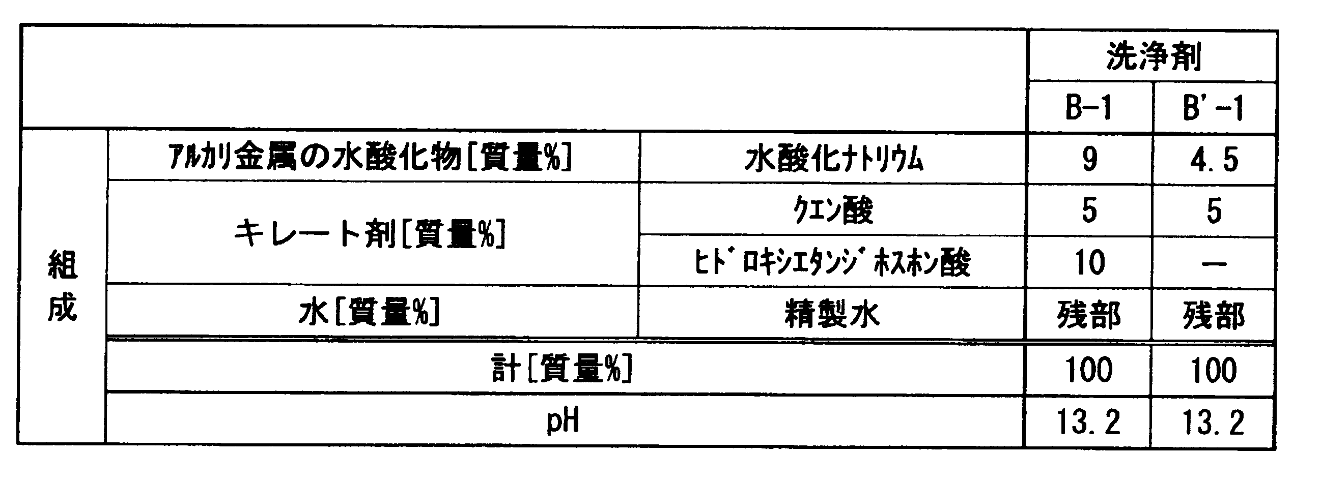
- Preparation Example 4 Preparation of Cleaning Agent B′-1 (Comparative Product of Cleaning Agent (B)) According to the composition shown in Table 2, each raw material was dispersed in water to obtain Cleaning Agent B′-1.
- a semiconductor substrate cleaned by the cleaning method of each example is placed in a class 1000 environment (in a clean room where the size of particles of 0.5 ⁇ m or more is controlled to 1000 or less per cubic foot of the substrate surface). ) And rotated at 1000 rpm and dried (spin drying).
- a wafer surface inspection apparatus Candela CS10 manufactured by KLA Tencor
- the number of particles of 0.5 ⁇ m or more remaining on the surface of the semiconductor substrate after drying was measured in a class 1000 environment. .
- the measured number of residual particles was classified into the following evaluation criteria to evaluate the cleanliness.
- a sapphire lump was sliced to obtain an original plate.
- the obtained original plate is fixed to a polishing jig with wax (hot melt adhesive) (wax fixing method), polished using colloidal silica as an abrasive, and a semiconductor substrate having a diameter of 4 inches (10 cm). I was obtained.
- a polishing machine was used for the polishing process.
- Examples 1 and 4 Comparative Examples 11 to 12, 15 to 16
- a semiconductor substrate of the type shown in Tables 4 and 5 is immersed in 10 L of “cleaning agent for first cleaning operation” in Tables 4 and 5, and ultrasonic waves are applied to the cleaning agent (50 ° C.) for 10 minutes (frequency) 36 kHz) (first cleaning operation).
- 10 L of “cleaning agent for second cleaning operation” in Tables 4 and 5 was set to 130 ° C., and the semiconductor substrate cleaned by the first cleaning operation was immersed in this for 10 minutes (second cleaning operation). The cleanliness of the semiconductor substrate cleaned by the second cleaning operation was evaluated, and the results are shown in Tables 4 and 5.
- Examples 2 to 3, Comparative Examples 13 to 14, 17 to 18 Except that the “cleaning agent for the first cleaning operation” in Tables 4 and 5 was diluted 20 times with pure water to obtain a cleaning solution, and the first cleaning operation was performed using 10 L (50 ° C.) of this cleaning solution.
- the semiconductor substrate was cleaned in the same manner as in Example 1. The cleanliness of the cleaned semiconductor substrate was evaluated, and the results are shown in Tables 4 and 5.
- Examples 5 to 6 In the same manner as in Example 1, the types of semiconductor substrates shown in Table 4 were cleaned by the first cleaning operation and the second cleaning operation.
- the semiconductor substrate cleaned in the second cleaning operation is immersed in 10 L of “cleaning agent for third cleaning operation” in Table 4, and ultrasonic waves are applied to the cleaning liquid (50 ° C.) for 10 minutes (frequency 36 kHz) (first frequency).
- Third washing operation 10 L of “the cleaning agent for the fourth cleaning operation” in Table 4 was set to 130 ° C., and the semiconductor substrate cleaned by the third cleaning operation was immersed in this for 10 minutes (fourth cleaning operation). The cleanliness of the semiconductor substrate cleaned by the fourth cleaning operation was evaluated, and the results are shown in Table 4.
- Examples 7 to 8 In the same manner as in Example 2, the types of semiconductor substrates shown in Table 4 were cleaned by the first cleaning operation and the second cleaning operation.
- the “cleaning agent for the third cleaning operation” in Table 4 was diluted 20 times with pure water to obtain a cleaning solution, and the semiconductor substrate cleaned by the second cleaning operation was immersed in this cleaning solution 10 L (50 ° C.), An ultrasonic wave was applied to the cleaning liquid for 10 minutes (frequency: 36 kHz) (third cleaning operation).
- 10 L of “the cleaning agent for the fourth cleaning operation” in Table 4 was set to 130 ° C., and the semiconductor substrate cleaned by the third cleaning operation was immersed in this for 10 minutes (fourth cleaning operation). The cleanliness of the semiconductor substrate cleaned by the fourth cleaning operation was evaluated, and the results are shown in Table 4.
- Example 9 Example 3 except that “cleaning agent for third cleaning operation” in Table 4 was diluted 20 times with pure water to obtain a cleaning solution, and the third cleaning operation was performed using 10 L (50 ° C.) of this cleaning solution.
- the semiconductor substrate was washed in the same manner as in FIG. The cleanliness of the cleaned semiconductor substrate was evaluated, and the results are shown in Table 4.
- Example 11 to 12 The “cleaning agent for the third cleaning operation” in Table 4 was used as a cleaning solution without diluting, and the third cleaning operation was performed using 10 L of this cleaning solution (50 ° C.).
- the semiconductor substrate was cleaned.
- the cleanliness of the cleaned semiconductor substrate was evaluated, and the results are shown in Table 4.
- Example 13 to 14 The semiconductor substrate was cleaned in the same manner as in Examples 9 to 10 except that the cleaning agent C-1 was changed to the cleaning agent C-2.
- the cleanliness of the cleaned semiconductor substrate was evaluated, and the results are shown in Table 4.
- Example 15 The semiconductor substrate was cleaned in the same manner as in Example 7 except that the cleaning agent C-1 was changed to the cleaning agent C-2.
- the cleanliness of the cleaned semiconductor substrate was evaluated, and the results are shown in Table 4.
- Comparative Examples 9 to 10 The same as in Comparative Example 7 except that the “cleaning agent for the second cleaning operation” in Table 5 was diluted 20 times with pure water to obtain a cleaning solution, and the second cleaning operation was performed using 10 L of this cleaning solution. The semiconductor substrate was cleaned. The cleanliness of the cleaned semiconductor substrate was evaluated, and the results are shown in Table 5.
- the semiconductor substrate I was cleaned by the following method. First, a semiconductor substrate was immersed in 10 L of acetone (EL grade reagent, manufactured by Kanto Chemical Co., Ltd.), and ultrasonic waves were applied to acetone at 25 ° C. for 10 minutes (first solvent cleaning). The semiconductor substrate cleaned by the first solvent cleaning was immersed in 10 L of isopropyl alcohol (EL grade reagent, manufactured by Kanto Chemical Co., Ltd.), and ultrasonic waves were applied to isopropyl alcohol at 25 ° C. for 5 minutes (second solvent cleaning). .
- acetone EL grade reagent, manufactured by Kanto Chemical Co., Ltd.
- the evaluation was 2 points (the number of residual particles was 2000).
- Comparative Example 20 The semiconductor substrate was cleaned in the same manner as in Comparative Example 19 except that the semiconductor substrate I was replaced with the semiconductor substrate II. When the cleanliness of the cleaned semiconductor substrate was evaluated, the evaluation was 2 points (the number of residual particles was 3500).
- Example 9 in which the cleaning agent A-1 was used for the first cleaning operation and the cleaning agent B-1 was used for the third cleaning operation, the cleanliness of the semiconductor substrate I could be improved more than in Examples 1 and 5. It was.
- Example 7 in which the cleaning agent B-1 was used in the first cleaning operation and the third cleaning operation, the cleanliness of the semiconductor substrate II was higher than that in Examples 2 and 12.
- Comparative Examples 1 to 6 having only the operation of cleaning with the cleaning agent A-1, the cleaning agent B-1 or the cleaning agent C-1, the evaluation of cleanliness was 1 point.
- Comparative Examples 7 to 10 where the cleaning agent C-1 was used for the first cleaning operation and the cleaning agent A-1 or the cleaning agent B-1 was used for the second cleaning operation, the cleanliness evaluation was one point. It was. Comparative Examples 11 to 14 using the cleaning agent C′-1 for the second cleaning operation, Comparative Examples 15 to 18 using the cleaning agent A′-1 or the cleaning agent B′-1 for the first cleaning operation, The evaluation of cleanliness was 2 points or less.
- Comparative Examples 19 to 20 are conventional cleaning methods for a semiconductor substrate, and are a combination of solvent cleaning (first and second solvent cleaning) and RCA cleaning (SPM cleaning to HPM cleaning). In Comparative Examples 19 to 20, the evaluation of cleanliness was 2 points. From these results, it was found that the cleanliness of the semiconductor substrate can be further increased by applying the present invention.
Landscapes
- Chemical & Material Sciences (AREA)
- Life Sciences & Earth Sciences (AREA)
- Engineering & Computer Science (AREA)
- Chemical Kinetics & Catalysis (AREA)
- Oil, Petroleum & Natural Gas (AREA)
- Wood Science & Technology (AREA)
- Organic Chemistry (AREA)
- Inorganic Chemistry (AREA)
- Health & Medical Sciences (AREA)
- Emergency Medicine (AREA)
- Cleaning Or Drying Semiconductors (AREA)
- Detergent Compositions (AREA)
Abstract
本発明の半導体基板の洗浄方法は、下記洗浄剤(A)又は下記洗浄剤(B)を用いて、研磨処理が施された半導体基板を洗浄する第一の洗浄操作と、前記第一の洗浄操作の後、下記洗浄剤(C)を用いて、前記半導体基板を洗浄する第二の洗浄操作とを備える。洗浄剤(A):炭化水素化合物と、グリコールエーテルと、界面活性剤とを含有する液体洗浄剤。洗浄剤(B):アルカリ金属の水酸化物と、ヒドロキシカルボン酸及びその塩から選択される1種以上と、1-ヒドロキシエタン-1,1-ジホスホン酸及びその塩から選択される1種以上とを含有する液体洗浄剤。洗浄剤(C):硫酸と過酸化水素とを含有し、硫酸濃度が50質量%以上である液体洗浄剤。
Description
本発明は、半導体基板の洗浄方法、及び半導体基板の製造方法に関する。
本願は、2012年11月16日に、日本に出願された特願2012-251819号に基づき優先権を主張し、その内容をここに援用する。
本願は、2012年11月16日に、日本に出願された特願2012-251819号に基づき優先権を主張し、その内容をここに援用する。
半導体基板の上には、薄膜が形成される。薄膜が形成された半導体基板は、半導体装置の製造に供される。半導体装置の機能の向上や歩留まりの向上を図るためには、薄膜を均一に形成する必要がある。このため、半導体基板には、表面が平坦でありかつ清浄であることが求められる。
例えば、発光ダイオード(LED)用の半導体基板である単結晶サファイア基板(以下、単にサファイア基板ということがある)は、次のように製造される。
まず、インゴットと呼ばれるサファイア塊をスライスすることによってサファイア基板を得る。このサファイア基板に、コロイダルシリカ等の研磨材で研磨処理を施す(研磨工程)。研磨処理が施されたサファイア基板には、研磨材や研磨カス等の微粒子汚れが付着している。そのため、サファイア基板を洗浄して表面を清浄化する(洗浄工程)。
こうして得られたサファイア基板の表面には、GaN、GaAs等の薄膜が形成される。薄膜が形成されたサファイア基板は、LED等に用いられる。
まず、インゴットと呼ばれるサファイア塊をスライスすることによってサファイア基板を得る。このサファイア基板に、コロイダルシリカ等の研磨材で研磨処理を施す(研磨工程)。研磨処理が施されたサファイア基板には、研磨材や研磨カス等の微粒子汚れが付着している。そのため、サファイア基板を洗浄して表面を清浄化する(洗浄工程)。
こうして得られたサファイア基板の表面には、GaN、GaAs等の薄膜が形成される。薄膜が形成されたサファイア基板は、LED等に用いられる。
上記研磨工程においては、サファイア基板を研磨治具に固定し、サファイア基板に研磨処理を施す。サファイア基板を研磨治具に固定する方法としては、ワックスを用いて、サファイア基板を研磨治具の台座に貼り付けて固定する方法(ワックス固定法)と、研磨治具に形成された窪みにサファイア基板を嵌め込んで固定する方法(嵌合固定法)とがある。
ワックス固定法で研磨処理が施されたサファイア基板には、ワックスが付着している。そのため、洗浄工程で微粒子汚れ及びワックスを除去する必要がある。
嵌合固定法で研磨処理が施されたサファイア基板の両面には、微粒子汚れが付着している。即ち、微粒子汚れの付着量が多い。そのため、洗浄工程で多量の微粒子汚れを除去する必要がある。
洗浄工程においては、研磨工程におけるサファイア基板の固定方法等に応じて、適切な洗浄方法が選択される。
ワックス固定法で研磨処理が施されたサファイア基板には、ワックスが付着している。そのため、洗浄工程で微粒子汚れ及びワックスを除去する必要がある。
嵌合固定法で研磨処理が施されたサファイア基板の両面には、微粒子汚れが付着している。即ち、微粒子汚れの付着量が多い。そのため、洗浄工程で多量の微粒子汚れを除去する必要がある。
洗浄工程においては、研磨工程におけるサファイア基板の固定方法等に応じて、適切な洗浄方法が選択される。
一般に、洗浄工程においては、例えば、アセトンやイソプロピルアルコール等の有機溶剤でサファイア基板を洗浄する(溶剤洗浄)。次いで、アンモニア、フッ酸、塩酸、硝酸、硫酸及び過酸化水素等を適宜組み合わせ、サファイア基板を多段階に洗浄する(RCA洗浄)。
しかし、溶剤洗浄とRCA洗浄との組み合わせにおいては、洗浄中にサファイア基板から脱離した微粒子汚れが、再びサファイア基板に付着して、サファイア基板の清浄度を高めにくいという問題がある。
加えて、RCA洗浄は、アンモニア、フッ酸、塩酸、硝酸、硫酸及び過酸化水素等の洗浄成分による洗浄処理を複雑に組み合わせるため、洗浄工程が煩雑である。
さらに、RCA洗浄には、前記洗浄成分の取り扱いが煩雑であるという問題がある。
しかし、溶剤洗浄とRCA洗浄との組み合わせにおいては、洗浄中にサファイア基板から脱離した微粒子汚れが、再びサファイア基板に付着して、サファイア基板の清浄度を高めにくいという問題がある。
加えて、RCA洗浄は、アンモニア、フッ酸、塩酸、硝酸、硫酸及び過酸化水素等の洗浄成分による洗浄処理を複雑に組み合わせるため、洗浄工程が煩雑である。
さらに、RCA洗浄には、前記洗浄成分の取り扱いが煩雑であるという問題がある。
こうした問題に対し、例えば、炭化水素化合物、グリコールエーテル、アニオン界面活性剤及び水を含有する洗浄剤組成物により半導体基板を洗浄する第1の洗浄工程と;水により半導体基板を洗浄する第2の洗浄工程と;水酸化第4級アンモニウム、窒素とカルボキシル基とを含むキレート剤、及び水を含有する第3の洗浄工程とを含み、第1の洗浄工程、第2の洗浄工程、第3の洗浄工程の順に半導体基板を洗浄する、半導体基板の洗浄方法が提案されている(例えば、特許文献1)。
しかしながら、半導体基板の洗浄方法には、より簡便に、半導体基板の清浄度をより高めることが求められている。
そこで、本発明は、より簡便に、半導体基板の清浄度をより高めることができる半導体基板の洗浄方法を提供することを目的とする。
そこで、本発明は、より簡便に、半導体基板の清浄度をより高めることができる半導体基板の洗浄方法を提供することを目的とする。
本発明の半導体基板の洗浄方法は、下記洗浄剤(A)又は下記洗浄剤(B)を用いて、研磨処理が施された半導体基板を洗浄する第一の洗浄操作と、
前記第一の洗浄操作の後、下記洗浄剤(C)を用いて、前記半導体基板を洗浄する第二の洗浄操作とを備える。
洗浄剤(A):炭化水素化合物と、グリコールエーテルと、界面活性剤とを含有する液体洗浄剤。
洗浄剤(B):アルカリ金属の水酸化物と、ヒドロキシカルボン酸及びその塩から選択される1種以上と、1-ヒドロキシエタン-1,1-ジホスホン酸及びその塩から選択される1種以上とを含有する液体洗浄剤。
洗浄剤(C):硫酸と過酸化水素とを含有し、硫酸濃度が50質量%以上である液体洗浄剤。
本発明の半導体基板の洗浄方法は、前記第二の洗浄操作の後、新たに前記洗浄剤(A)又は前記洗浄剤(B)を用いて、前記半導体基板を洗浄する第三の洗浄操作と、前記第三の洗浄操作の後、新たに前記洗浄剤(C)を用いて、前記半導体基板を洗浄する第四の洗浄操作とをさらに備えることが好ましい。
本発明の半導体基板の洗浄方法においては、前記第一の洗浄操作には、前記洗浄剤(A)を用い、前記第三の洗浄操作には、前記洗浄剤(B)を用いることがより好ましい。
また、本発明の半導体基板の洗浄方法においては、前記第一の洗浄操作には、前記洗浄剤(B)を用い、前記第三の洗浄操作には、前記洗浄剤(B)を用いることがより好ましい。
また、本発明の半導体基板の洗浄方法においては、前記半導体基板は、単結晶サファイア基板であってもよい。
前記第一の洗浄操作の後、下記洗浄剤(C)を用いて、前記半導体基板を洗浄する第二の洗浄操作とを備える。
洗浄剤(A):炭化水素化合物と、グリコールエーテルと、界面活性剤とを含有する液体洗浄剤。
洗浄剤(B):アルカリ金属の水酸化物と、ヒドロキシカルボン酸及びその塩から選択される1種以上と、1-ヒドロキシエタン-1,1-ジホスホン酸及びその塩から選択される1種以上とを含有する液体洗浄剤。
洗浄剤(C):硫酸と過酸化水素とを含有し、硫酸濃度が50質量%以上である液体洗浄剤。
本発明の半導体基板の洗浄方法は、前記第二の洗浄操作の後、新たに前記洗浄剤(A)又は前記洗浄剤(B)を用いて、前記半導体基板を洗浄する第三の洗浄操作と、前記第三の洗浄操作の後、新たに前記洗浄剤(C)を用いて、前記半導体基板を洗浄する第四の洗浄操作とをさらに備えることが好ましい。
本発明の半導体基板の洗浄方法においては、前記第一の洗浄操作には、前記洗浄剤(A)を用い、前記第三の洗浄操作には、前記洗浄剤(B)を用いることがより好ましい。
また、本発明の半導体基板の洗浄方法においては、前記第一の洗浄操作には、前記洗浄剤(B)を用い、前記第三の洗浄操作には、前記洗浄剤(B)を用いることがより好ましい。
また、本発明の半導体基板の洗浄方法においては、前記半導体基板は、単結晶サファイア基板であってもよい。
本発明の半導体基板の製造方法は、前記の本発明の半導体基板の洗浄方法で半導体基板を洗浄する洗浄工程を備える。
言い換えると、本発明の半導体基板の製造方法は、インゴットをスライスして基板を作成する基板製造工程と、
基板に研磨材を用いて研磨処理を施す研磨工程と、
研磨処理が施された半導体基板を本発明の半導体基板の洗浄方法を用いて洗浄する洗浄工程とを備える。
言い換えると、本発明の半導体基板の製造方法は、インゴットをスライスして基板を作成する基板製造工程と、
基板に研磨材を用いて研磨処理を施す研磨工程と、
研磨処理が施された半導体基板を本発明の半導体基板の洗浄方法を用いて洗浄する洗浄工程とを備える。
本発明の半導体基板の洗浄方法によれば、清浄度がより高められた半導体基板をより簡便に製造できる。
(半導体基板の製造方法)
本発明の半導体基板の製造方法は、研磨処理が施された半導体基板を本発明の半導体基板の洗浄方法(以下、単に洗浄方法ということがある)で洗浄する洗浄工程を備える。
本発明の半導体基板の製造方法は、研磨処理が施された半導体基板を本発明の半導体基板の洗浄方法(以下、単に洗浄方法ということがある)で洗浄する洗浄工程を備える。
<洗浄工程>
洗浄工程は、研磨処理が施された半導体基板を洗浄する工程であり、後述する第一の洗浄操作と後述する第二の洗浄操作とを備える。
洗浄工程は、研磨処理が施された半導体基板を洗浄する工程であり、後述する第一の洗浄操作と後述する第二の洗浄操作とを備える。
≪第一の洗浄操作≫
第一の洗浄操作においては、下記洗浄剤(A)又は下記洗浄剤(B)を用いて、研磨処理が施された半導体基板を洗浄する。
洗浄剤(A):炭化水素化合物と、グリコールエーテルと、界面活性剤とを含有する液体洗浄剤。
洗浄剤(B):アルカリ金属の水酸化物と、ヒドロキシカルボン酸及びその塩から選択される1種以上(ヒドロキシカルボン酸(塩))と、1-ヒドロキシエタン-1,1-ジホスホン酸及びその塩から選択される1種以上(1-ヒドロキシエタン-1,1-ジホスホン酸(塩))とを含有する液体洗浄剤。
第一の洗浄操作においては、下記洗浄剤(A)又は下記洗浄剤(B)を用いて、研磨処理が施された半導体基板を洗浄する。
洗浄剤(A):炭化水素化合物と、グリコールエーテルと、界面活性剤とを含有する液体洗浄剤。
洗浄剤(B):アルカリ金属の水酸化物と、ヒドロキシカルボン酸及びその塩から選択される1種以上(ヒドロキシカルボン酸(塩))と、1-ヒドロキシエタン-1,1-ジホスホン酸及びその塩から選択される1種以上(1-ヒドロキシエタン-1,1-ジホスホン酸(塩))とを含有する液体洗浄剤。
[洗浄剤(A)]
洗浄剤(A)は、炭化水素化合物と、グリコールエーテルと、界面活性剤とを含有する液体洗浄剤である。洗浄剤(A)は、微粒子汚れに対して高い洗浄力を有し、かつワックス等の油脂汚れに対して特に高い洗浄力を有する。
洗浄剤(A)は、炭化水素化合物と、グリコールエーテルと、界面活性剤とを含有する液体洗浄剤である。洗浄剤(A)は、微粒子汚れに対して高い洗浄力を有し、かつワックス等の油脂汚れに対して特に高い洗浄力を有する。
洗浄剤(A)は、炭化水素化合物を含有することで、半導体基板に付着したワックス等の汚れを良好に除去できる。
従って、ワックス固定法により研磨処理が施された半導体基板を洗浄する場合には、洗浄剤(A)を用いることが好ましい。
従って、ワックス固定法により研磨処理が施された半導体基板を洗浄する場合には、洗浄剤(A)を用いることが好ましい。
炭化水素化合物は、飽和炭化水素化合物でもよく、不飽和炭化水素化合物でもよい。例えば、パラフィン系炭化水素化合物、オレフィン系炭化水素化合物、芳香族炭化水素化合物、アルキルベンゼン系炭化水素化合物、アルキルナフタレン系炭化水素化合物等が挙げられる。これらの炭化水素は、1種単独で用いられてもよいし、2種以上が組み合わされて用いられてもよい。
炭化水素化合物としては、例えば、下記一般式(a1)で表される飽和炭化水素化合物、及び下記一般式(a2)で表される不飽和炭化水素化合物から選択される1種以上の化合物が好ましい。
CmH2m+2 (a1)
式(a1)中、mは8~20が好ましく、10~18がより好ましく、10~14がさらに好ましい。mが上記下限値未満では、引火性が高くなる。mが上記上限値超では、洗浄剤(A)の配合安定性が低下し、洗浄剤(A)が白濁しやすい。
CnH2n (a2)
式(a2)中、nは8~20が好ましく、10~18がより好ましい。nが上記下限値未満では、引火性が高くなる。nが上記上限値超では、洗浄剤(A)の配合安定性が低下し、洗浄剤(A)が白濁しやすい。
炭化水素化合物の市販品としては、例えば、カクタスノルマルパラフィンN12D(商品名、(a1)式中のmが12であるドデカン、JX日鉱日石エネルギー株式会社製)、流動パラフィンNo.30(商品名、(a1)式中のmが12~14の化合物、中央化成株式会社製)、リニアレン14(商品名、(a2)式中のnが14の化合物、出光興産株式会社製)等が挙げられる。
洗浄剤(A)中の炭化水素化合物の含有量は、炭化水素化合物の種類等を勘案して決定され、例えば、1~20質量%が好ましく、3~10質量%がより好ましい。
洗浄剤(A)は、グリコールエーテルを含有することで、炭化水素化合物及び界面活性剤が分散媒に可溶化されて、液安定性が高められる。
グリコールエーテルとしては、例えば、下記一般式(a10)で表される化合物が挙げられる。
グリコールエーテルとしては、例えば、下記一般式(a10)で表される化合物が挙げられる。
R1-O-(R3O)p-R2 (a10)
式(a10)中、R1は、炭素数4~8の直鎖もしくは分岐鎖のアルキル基、炭素数4~8の直鎖もしくは分岐鎖のアルケニル基、フェニル基又はベンジル基であり、中でも、直鎖もしくは分岐鎖のアルキル基が好ましい。
R3Oは、炭素数2~4のオキシアルキレン基であり、構造中に少なくとも1単位のオキシエチレン基を含む。
pはR3Oの平均繰り返し数を示す1~4の数である。
R2は水素基、炭素数1~4の直鎖もしく分岐鎖のアルキル基、又は炭素数1~4の直鎖もしく分岐鎖のアルケニル基である。
R3Oは、炭素数2~4のオキシアルキレン基であり、構造中に少なくとも1単位のオキシエチレン基を含む。
pはR3Oの平均繰り返し数を示す1~4の数である。
R2は水素基、炭素数1~4の直鎖もしく分岐鎖のアルキル基、又は炭素数1~4の直鎖もしく分岐鎖のアルケニル基である。
グリコールエーテルとしては、ジエチレングリコールモノヘキシルエーテル(C6H13O(CH2CH2O)2H、例えば日本乳化剤株式会社製のヘキシルジグリコール(商品名))、ジプロピレングリコールモノブトキシエチルエーテル(C4H9OC2H4O(C3H6O)2H、例えばライオン株式会社製のレオソルブ703B(商品名))、ジエチレングリコールジブチルエーテル(C4H9O(C2H4O)2C4H9、例えば日本乳化剤株式会社製のジブチルジグリコール(商品名))、トリエチレングリコールモノブチルエーテル(C4H9O(CH2CH2O)3H、例えばKHネオケム株式会社製のブチセノール30(商品名))、エチレングリコールモノ(2-エチルヘキシル)エーテル(C8H17O(CH2CH2O)2H、例えば日本乳化剤株式会社製の2エチルへキシルジグリコール(商品名))、及びジエチレングリコールモノブチルエーテル(C4H9O(C2H4O)2H、例えば日本乳化剤株式会社製のブチルジグリコール(商品名))等が挙げられる。中でも、ブチルジグリコール、ジブチルジグリコール、及び2エチルへキシルジグリコールが好ましい。これらのグリコールエーテルは、1種単独で用いられてもよいし、2種以上が組み合わされて用いられてもよい。
洗浄剤(A)中のグリコールエーテルの含有量は、グリコールエーテルの種類等を勘案して決定され、例えば、5~50質量%が好ましく、15~40質量%がより好ましい。
洗浄剤(A)は界面活性剤を含有することで、洗浄対象である半導体基板に付着した微粒子汚れやワックス等をより良好に除去できる。
界面活性剤としては、アニオン界面活性剤及びノニオン界面活性剤等が挙げられ、中でも、アニオン界面活性剤が好ましい。
界面活性剤としては、アニオン界面活性剤及びノニオン界面活性剤等が挙げられ、中でも、アニオン界面活性剤が好ましい。
アニオン界面活性剤としては、特に限定されないが、例えば、ジアルキルスルホコハク酸塩が好ましい。ジアルキルスルホコハク酸塩におけるアルキル基の種類及び塩の種類は、特に限定されない。ジアルキルスルホコハク酸塩としては、例えば、ジアルキルスルホコハク酸ナトリウム塩及びジアルキルスルホコハク酸アンモニウム塩等が挙げられる。中でも、ジアルキルスルホコハク酸ナトリウム塩が好ましく、安価である点及び入手しやすい点から、ジオクチルスルホコハク酸ナトリウム塩がより好ましい。これらのアニオン界面活性剤は、1種単独で用いられてもよいし、2種以上が組み合わされて用いられてもよい。
ジオクチルスルホコハク酸ナトリウム塩の市販品としては、リパール870P(商品名、ライオン株式会社製)等が挙げられる。
ジオクチルスルホコハク酸ナトリウム塩の市販品としては、リパール870P(商品名、ライオン株式会社製)等が挙げられる。
ノニオン界面活性剤としては、下記一般式(a20)で表される化合物が挙げられる。
R11-O-(R12O)r-H ・・・(a20)
式(a20)中、R11は炭素数8~20の直鎖もしくは分岐鎖のアルキル基、又は炭素数8~20の直鎖もしくは分岐鎖のアルケニル基、フェニル基又はベンジル基である。
R11は、アルキル基又はアルケニル基が好ましい。
R11の炭素数は、8~14が好ましく、8~10がより好ましい。
R12Oは炭素数2~4のオキシアルキレン基であり、構造中に少なくとも1単位のオキシエチレン基を含む。R12Oは、炭素数2~3のオキシアルキレン基が好ましい。
rはR12Oの平均繰り返し数を示す8~20の数であり、12~20が好ましく、14~20がより好ましい。
R11は、アルキル基又はアルケニル基が好ましい。
R11の炭素数は、8~14が好ましく、8~10がより好ましい。
R12Oは炭素数2~4のオキシアルキレン基であり、構造中に少なくとも1単位のオキシエチレン基を含む。R12Oは、炭素数2~3のオキシアルキレン基が好ましい。
rはR12Oの平均繰り返し数を示す8~20の数であり、12~20が好ましく、14~20がより好ましい。
式(a20)で表される化合物としては、ポリオキシアルキレンアルキルエーテル、ポリオキシアルキレンアルキルフェニルエーテル、ポリオキシアルキレンアリルフェニルエーテル等が挙げられる。
式(a20)で表される化合物の市販品としては、ドバノックスシリーズ(商品名、ライオン株式会社製)、レオコールシリーズ(商品名、ライオン株式会社製)、レオックスシリーズ(商品名、ライオン株式会社製)、ニューコールシリーズ(商品名、日本乳化剤株式会社製)、ソフタノールシリーズ(商品名、株式会社日本触媒製)、ノイゲンシリーズ(商品名、第一工業製薬株式会社製)等が挙げられる。中でも、C10H21O(CH2CH2O)14Hで表される化合物(例えば、第一工業製薬株式会社製のノイゲンXL-140(商品名))、及びC8H17O(CH2CH2O)20Hで表される化合物(例えば日本乳化剤株式会社製のニューコール1020(商品名))が好ましい。これらのノニオン界面活性剤は、1種単独で用いられてもよいし、2種以上が組み合わされて用いられてもよい。
式(a20)で表される化合物の市販品としては、ドバノックスシリーズ(商品名、ライオン株式会社製)、レオコールシリーズ(商品名、ライオン株式会社製)、レオックスシリーズ(商品名、ライオン株式会社製)、ニューコールシリーズ(商品名、日本乳化剤株式会社製)、ソフタノールシリーズ(商品名、株式会社日本触媒製)、ノイゲンシリーズ(商品名、第一工業製薬株式会社製)等が挙げられる。中でも、C10H21O(CH2CH2O)14Hで表される化合物(例えば、第一工業製薬株式会社製のノイゲンXL-140(商品名))、及びC8H17O(CH2CH2O)20Hで表される化合物(例えば日本乳化剤株式会社製のニューコール1020(商品名))が好ましい。これらのノニオン界面活性剤は、1種単独で用いられてもよいし、2種以上が組み合わされて用いられてもよい。
洗浄剤(A)中、上述の界面活性剤は、1種単独で用いられてもよいし、2種以上が組み合わされて用いられてもよい。
洗浄剤(A)中の界面活性剤の含有量は、界面活性剤の種類等を勘案して決定され、例えば、1~20質量%が好ましく、3~15質量%がより好ましい。
洗浄剤(A)中の界面活性剤の含有量は、界面活性剤の種類等を勘案して決定され、例えば、1~20質量%が好ましく、3~15質量%がより好ましい。
洗浄剤(A)は、分散媒である水、キレート剤、酸化防止剤、防錆剤、消泡剤、pH調整剤等の任意成分を含有できる。
洗浄剤(A)中の水の含有量は、例えば、30~80質量%が好ましい。
洗浄剤(A)中の水の含有量は、例えば、30~80質量%が好ましい。
キレート剤としては、クエン酸、酒石酸、リンゴ酸、エチレンジアミンテトラ酢酸(EDTA)、トリエチレンテトラ酢酸(TTHA)、メチルグリシン二酢酸(MGDA)、1,3-プロパン-2-ジアミン四酢酸(PDTA)、ヒドロキシエチルエチレンジアミントリ酢酸(HEDTA)、ヒドロキシエチルイミノジ酢酸(HIDA)、ニトリロトリ酢酸(NTA)、ジエチレントリアミンペンタ酢酸(DTPA)、プロピレンジアミンテトラ酢酸、エチレンジアミンテトラプロピオン酸、シクロヘキサン-1,2-ジアミンテトラ酢酸、イミノジコハク酸、アスパラギン酸ジ酢酸、β-アラニンジ酢酸、ヒドロキシイミノジコハク酸及びこれらの酸の塩が挙げられる。塩を形成する塩基としては、ナトリウム、カリウム、カルシウム、マグネシウム等が挙げられる。
酸化防止剤としては、例えば、2,6-ジ-t-ブチルフェノール、2-t-ブチル-4-メトキシフェノール、又は2,4-ジメチル-6-t-ブチルフェノール等のフェノール系酸化防止剤;モノオクチルジフェニルアミン又はモノノニルジフェニルアミン等のモノアルキルジフェニルアミン、4,4’-ジブチルジフェニルアミン又は4,4’-ジペンチルジフェニルアミン等のジアルキルジフェニルアミン、テトラブチルジフェニルアミン又はテトラヘキシルジフェニルアミン等のポリアルキルジフェニルアミン、α-ナフチルアミン又はフェニル-α-ナフチルアミン等のナフチルアミン等のアミン系酸化防止剤;フェノチアジン、ペンタエリスリトール-テトラキス-(3-ラウリルチオプロピオネート)、又はビス(3,5-tert-ブチル-4-ヒドロキシベンジル)スルフィド等の硫黄系化合物;及びビス(2,4-ジ-t-ブチルフェニル)ペンタエリスリトールジホスファイト、フェニルジイソデシルホスフィト、ジフェニルジイソオクチルホスファイト、又はトリフェニルホスファイト等のリン系酸化防止剤等が挙げられる。
防錆剤としては、例えば、ベンゾトリアゾール、トリルトリアゾール、炭素数2~10の炭化水素基を有するベンゾトリアゾール、ベンゾイミダゾール、炭素数2~20の炭化水素基を有するイミダゾール、炭素数2~20の炭化水素基を有するチアゾール、又は2-メルカプトベンゾチアゾール等の含窒素有機防錆剤;ドデセニルコハク酸ハーフエステル、オクタデセニルコハク酸無水物、又はドデセニルコハク酸アミド等のアルキルコハク酸及びアルケニルコハク酸;並びにソルビタンモノオレエート、グリセリンモノオレエート、又はペンタエリスリトールモノオレエート等の多価アルコール部分エステル等が挙げられる。
消泡剤としては、例えば、ジメチルシリコーン、フルオロシリコーン、又はポリエーテルシリコーン等を含むシリコーン消泡剤等が挙げられる。
酸性のpH調整剤としては、上記キレート剤で記載した以外のリン酸及びカルボン酸等が挙げられる。
カルボン酸としては、例えば、ブタン酸、ペンタン酸、ヘキサン酸、ヘプタン酸、オクタン酸、ノナン酸、デカン酸、又はドデカン酸等の脂肪族カルボン酸類;及び安息香酸、パラターシャリーブチル安息香酸、フタル酸、イソフタル酸、又はテレフタル酸等の芳香族カルボン酸類が好ましい。
アルカリ性のpH調整剤としては、アルカノールアミン、第4級アンモニウム水酸化物、及び無機塩が挙げられる。
アルカノールアミンとしては、例えば、モノエタノールアミン、ジエタノールアミン、及びトリエタノールアミンが挙げられる。
第4級アンモニウム水酸化物としては、例えば、テトラメチルアンモニウムハイドロオキサイド、トリメチルヒドロキシエチルアンモニウムハイドロオキサイド、メチルトリヒドロキシエチルアンモニウムハイドロオキサイド、ジメチルジヒドロキシエチルアンモニウムハイドロオキサイド、テトラエチルアンモニウムハイドロオキサイド、及びトリメチルエチルアンモニウムハイドロオキサイド等が挙げられる。
無機塩としては、例えば、水酸化ナトリウム及び水酸化カリウム等が挙げられる。
洗浄剤(A)中のpH調整剤の含有量は、pH調整剤の種類等に応じて決定される。
カルボン酸としては、例えば、ブタン酸、ペンタン酸、ヘキサン酸、ヘプタン酸、オクタン酸、ノナン酸、デカン酸、又はドデカン酸等の脂肪族カルボン酸類;及び安息香酸、パラターシャリーブチル安息香酸、フタル酸、イソフタル酸、又はテレフタル酸等の芳香族カルボン酸類が好ましい。
アルカリ性のpH調整剤としては、アルカノールアミン、第4級アンモニウム水酸化物、及び無機塩が挙げられる。
アルカノールアミンとしては、例えば、モノエタノールアミン、ジエタノールアミン、及びトリエタノールアミンが挙げられる。
第4級アンモニウム水酸化物としては、例えば、テトラメチルアンモニウムハイドロオキサイド、トリメチルヒドロキシエチルアンモニウムハイドロオキサイド、メチルトリヒドロキシエチルアンモニウムハイドロオキサイド、ジメチルジヒドロキシエチルアンモニウムハイドロオキサイド、テトラエチルアンモニウムハイドロオキサイド、及びトリメチルエチルアンモニウムハイドロオキサイド等が挙げられる。
無機塩としては、例えば、水酸化ナトリウム及び水酸化カリウム等が挙げられる。
洗浄剤(A)中のpH調整剤の含有量は、pH調整剤の種類等に応じて決定される。
洗浄剤(A)のpHは、洗浄剤(A)の組成や、半導体基板の材質等を勘案して、適宜決定される。
洗浄剤(A)は、従来公知の液体洗浄剤の調製方法に準じて調製される。
例えば、分散媒である水に炭化水素化合物、グリコールエーテル、界面活性剤及び必要に応じて任意成分を分散することで、洗浄剤(A)を調製できる。
例えば、分散媒である水に炭化水素化合物、グリコールエーテル、界面活性剤及び必要に応じて任意成分を分散することで、洗浄剤(A)を調製できる。
[洗浄剤(B)]
洗浄剤(B)は、アルカリ金属の水酸化物と、ヒドロキシカルボン酸(塩)と、1-ヒドロキシエタン-1,1-ジホスホン酸(塩)とを含有する液体洗浄剤である。洗浄剤(B)は、半導体基板から微粒子汚れを良好に剥離し、かつ微粒子汚れの再付着をより良好に防止できるため、微粒子汚れに対する洗浄力が特に高い。即ち、洗浄剤(B)は、微粒子汚れの付着量が多い半導体基板を洗浄するのに好適である。
従って、嵌合固定法により研磨処理が施された半導体基板を洗浄する場合には、洗浄剤(B)を用いることが好ましい。
洗浄剤(B)は、アルカリ金属の水酸化物と、ヒドロキシカルボン酸(塩)と、1-ヒドロキシエタン-1,1-ジホスホン酸(塩)とを含有する液体洗浄剤である。洗浄剤(B)は、半導体基板から微粒子汚れを良好に剥離し、かつ微粒子汚れの再付着をより良好に防止できるため、微粒子汚れに対する洗浄力が特に高い。即ち、洗浄剤(B)は、微粒子汚れの付着量が多い半導体基板を洗浄するのに好適である。
従って、嵌合固定法により研磨処理が施された半導体基板を洗浄する場合には、洗浄剤(B)を用いることが好ましい。
アルカリ金属の水酸化物としては、例えば、水酸化ナトリウム及び水酸化カリウムが挙げられる。アルカリ金属の水酸化物は、後述するヒドロキシカルボン酸(塩)又は1-ヒドロキシエタン-1,1-ジホスホン酸(塩)との相乗効果により、洗浄力を高められる。
洗浄剤(B)中におけるアルカリ金属の水酸化物の含有量は、0.1~15質量%が好ましく、1~10質量%がより好ましい。
洗浄剤(B)中におけるアルカリ金属の水酸化物の含有量は、0.1~15質量%が好ましく、1~10質量%がより好ましい。
ヒドロキシカルボン酸(塩)は、アルカリ金属の水酸化物、後述する1-ヒドロキシエタン-1,1-ジホスホン酸(塩)との相乗効果により、洗浄力を高められる。
ヒドロキシカルボン酸(塩)としては、クエン酸、サリチル酸、グルコン酸、グリコール酸、乳酸、ヒドロキシ酪酸、リンゴ酸、酒石酸、没食子酸、ヒドロキシイミノジ酢酸(HIDA)、ヒドロキシイミノジコハク酸(HIDS)、ヒドロキシエチルエチレンジアミン三酢酸(HEDTA)、ジヒドロキシエチルグリシン(DHEG)、1,3-ジアミノ-2-ヒドロキシプロパン四酢酸(DTPA-OH)、ヘプトグルコン酸及びこれらの塩等が挙げられる。ヒドロキシカルボン酸塩を構成する塩としては、ナトリウム、カリウム等が挙げられる。中でも、クエン酸又はその塩が好ましく、クエン酸ナトリウムがより好ましい。これらのヒドロキシカルボン酸(塩)は、1種単独で用いられてもよいし、2種以上が組み合わされて用いられてもよい。
洗浄剤(B)中のヒドロキシカルボン酸(塩)の含有量は、0.1~15質量%が好ましく、1~10質量%がより好ましい。
ヒドロキシカルボン酸(塩)としては、クエン酸、サリチル酸、グルコン酸、グリコール酸、乳酸、ヒドロキシ酪酸、リンゴ酸、酒石酸、没食子酸、ヒドロキシイミノジ酢酸(HIDA)、ヒドロキシイミノジコハク酸(HIDS)、ヒドロキシエチルエチレンジアミン三酢酸(HEDTA)、ジヒドロキシエチルグリシン(DHEG)、1,3-ジアミノ-2-ヒドロキシプロパン四酢酸(DTPA-OH)、ヘプトグルコン酸及びこれらの塩等が挙げられる。ヒドロキシカルボン酸塩を構成する塩としては、ナトリウム、カリウム等が挙げられる。中でも、クエン酸又はその塩が好ましく、クエン酸ナトリウムがより好ましい。これらのヒドロキシカルボン酸(塩)は、1種単独で用いられてもよいし、2種以上が組み合わされて用いられてもよい。
洗浄剤(B)中のヒドロキシカルボン酸(塩)の含有量は、0.1~15質量%が好ましく、1~10質量%がより好ましい。
1-ヒドロキシエタン-1,1-ジホスホン酸(塩)は、アルカリ金属の水酸化物又はヒドロキシカルボン酸(塩)との相乗効果により、洗浄力を高められる。
1-ヒドロキシエタン-1,1-ジホスホン酸(塩)としては、例えば、1-ヒドロキシエタン-1,1-ジホスホン酸、及び1-ヒドロキシエタン-1,1-ジホスホン酸のナトリウム塩、カリウム塩、アンモニウム塩、モノエタノールアミン塩、ジエタノールアミン塩又はトリエタノールアミン塩等が挙げられ、中でも、1-ヒドロキシエタン-1,1-ジホスホン酸のナトリウム塩が好ましい。
洗浄剤(B)中の1-ヒドロキシエタン-1,1-ジホスホン酸(塩)の含有量は、0.1~20質量%が好ましく、1~15質量%がより好ましい。
1-ヒドロキシエタン-1,1-ジホスホン酸(塩)としては、例えば、1-ヒドロキシエタン-1,1-ジホスホン酸、及び1-ヒドロキシエタン-1,1-ジホスホン酸のナトリウム塩、カリウム塩、アンモニウム塩、モノエタノールアミン塩、ジエタノールアミン塩又はトリエタノールアミン塩等が挙げられ、中でも、1-ヒドロキシエタン-1,1-ジホスホン酸のナトリウム塩が好ましい。
洗浄剤(B)中の1-ヒドロキシエタン-1,1-ジホスホン酸(塩)の含有量は、0.1~20質量%が好ましく、1~15質量%がより好ましい。
洗浄剤(B)は、洗浄剤(A)と同様に、分散媒である水や、pH調整剤(但し、アルカリ金属の水酸化物を除く)、キレート剤(但し、ヒドロキシカルボン酸(塩)及び1-ヒドロキシー1,1-ジホスホン酸(塩)を除く)、界面活性剤、酸化防止剤、防錆剤、又は消泡剤等の任意成分を含有できる。
洗浄剤(B)中の水の含有量は、例えば、30~80質量%が好ましい。
洗浄剤(B)中の水の含有量は、例えば、30~80質量%が好ましい。
洗浄剤(B)のpHは、洗浄剤(B)の組成や、半導体基板の材質等を勘案して、適宜決定される。
洗浄剤(B)は、従来公知の液体洗浄剤の調製方法に準じて調製される。
例えば、分散媒である水にアルカリ金属の水酸化物、ヒドロキシカルボン酸(塩)、1-ヒドロキシエタン-1,1-ジホスホン酸(塩)及び必要に応じて任意成分を分散することで、洗浄剤(B)を調製できる。
例えば、分散媒である水にアルカリ金属の水酸化物、ヒドロキシカルボン酸(塩)、1-ヒドロキシエタン-1,1-ジホスホン酸(塩)及び必要に応じて任意成分を分散することで、洗浄剤(B)を調製できる。
第一の洗浄操作は、例えば、洗浄剤(A)又は洗浄剤(B)を含有する洗浄液(第一の洗浄液)に、研磨処理が施された半導体基板(以下、研磨済基板ということがある)を浸漬する方法、第一の洗浄液に研磨済基板を浸漬しつつ、超音波を印加する方法(超音波印加法)、及び研磨済基板に第一の洗浄液を吹き付け、その後に拭き取る方法等が挙げられる。
中でも、第一の洗浄操作としては、第一の洗浄液に研磨済基板を浸漬しつつ、超音波を印加する方法が好ましい。
中でも、第一の洗浄操作としては、第一の洗浄液に研磨済基板を浸漬しつつ、超音波を印加する方法が好ましい。
研磨済基板としては、例えば、未研磨の半導体基板(以下、原板ということがある)に、コロイダルシリカ等の研磨材で研磨処理が施された(研磨工程)ものが挙げられる。研磨済基板としては、単結晶サファイア基板、シリコン基板、及びSiC基板等が挙げられ、中でも、単結晶サファイア基板が好ましい。
研磨工程における原板の研磨方法としては、ワックス固定法又は嵌合固定法によって原板を固定し、研磨材を含むスラリーを原板に供給しつつ研磨機で原板を研磨する方法が挙げられる。
研磨工程における原板の研磨方法としては、ワックス固定法又は嵌合固定法によって原板を固定し、研磨材を含むスラリーを原板に供給しつつ研磨機で原板を研磨する方法が挙げられる。
第一の洗浄液中の洗浄剤の含有量は、洗浄剤の種類等を勘案して適宜決定される。洗浄剤(A)を用いる場合、洗浄剤(A)をそのまま第一の洗浄液として用いることが好ましい。洗浄剤(B)を用いる場合、洗浄剤(B)の含有量が1~20質量%となるように水で希釈して、第一の洗浄液とすることが好ましい。
超音波印加法に用いられる装置としては、特に限定されないが、例えば、UO300FB-PY(株式会社日立国際電気製)等が挙げられる。
第一の洗浄操作における温度条件は、洗浄剤の種類等に応じて決定される。洗浄剤(A)を用いる場合の温度条件としては、例えば、40~60℃が好ましい。洗浄剤(B)を用いる場合の温度条件としては、例えば、25~60℃が好ましい。
第一の洗浄操作における時間としては、洗浄方法等に応じて適宜決定され、超音波印加法においては、例えば、5~20分間が好ましい。
第一の洗浄操作における温度条件は、洗浄剤の種類等に応じて決定される。洗浄剤(A)を用いる場合の温度条件としては、例えば、40~60℃が好ましい。洗浄剤(B)を用いる場合の温度条件としては、例えば、25~60℃が好ましい。
第一の洗浄操作における時間としては、洗浄方法等に応じて適宜決定され、超音波印加法においては、例えば、5~20分間が好ましい。
第一の洗浄操作は、研磨済基板を第一の洗浄液で洗浄した後、研磨済基板を水で濯ぐ第一の濯ぎ処理を備えてもよい。
≪第二の洗浄操作≫
第二の洗浄操作においては、下記洗浄剤(C)を用いて、第一の洗浄操作で洗浄された半導体基板を洗浄する。
洗浄剤(C):硫酸と過酸化水素とを含有し、硫酸濃度が50質量%以上である液体洗浄剤。
第一の洗浄操作の後に第二の洗浄操作を設けることで、半導体基板に付着した微粒子汚れ等をより良好に除去できる。
第二の洗浄操作においては、下記洗浄剤(C)を用いて、第一の洗浄操作で洗浄された半導体基板を洗浄する。
洗浄剤(C):硫酸と過酸化水素とを含有し、硫酸濃度が50質量%以上である液体洗浄剤。
第一の洗浄操作の後に第二の洗浄操作を設けることで、半導体基板に付着した微粒子汚れ等をより良好に除去できる。
[洗浄剤(C)]
洗浄剤(C)は、硫酸と過酸化水素とを含有する。
洗浄剤(C)中の硫酸の含有量は、50質量%以上であり、75質量%以上が好ましく、80質量%以上がさらに好ましい。上記下限値未満では、微粒子汚れに対する洗浄力の向上が図れない。
洗浄剤(C)は、硫酸と過酸化水素とを含有する。
洗浄剤(C)中の硫酸の含有量は、50質量%以上であり、75質量%以上が好ましく、80質量%以上がさらに好ましい。上記下限値未満では、微粒子汚れに対する洗浄力の向上が図れない。
洗浄剤(C)中の過酸化水素の含有量は、1~30質量%が好ましく、1~20質量%がより好ましく、1~10質量%が特に好ましく、5~20質量%がより好ましい。上記下限値未満では、過酸化水素が少なすぎて微粒子汚れに対する洗浄力が低下するおそれがある。上記上限値超では、硫酸と過酸化水素とが激しく反応するおそれがある。
洗浄剤(C)は、任意成分として水を含んでもよい。
第二の洗浄操作における洗浄方法としては、洗浄剤(C)を含有する第二の洗浄液に、第一の洗浄操作で洗浄された研磨済基板(一次洗浄済基板)を浸漬する方法が挙げられる。第二の洗浄液としては、洗浄剤(C)が希釈されずに用いられる。第二の洗浄操作は、例えば、硫酸と過酸化水素とを予め混合して第二の洗浄液とし、この第二の洗浄液に一次洗浄済基板を浸漬する方法、及び、容器に硫酸を入れ、この容器中の硫酸に一次洗浄済基板を浸漬し、次いで、硫酸に過酸化水素を加える方法等が挙げられる。硫酸に過酸化水素を加えると、カロ酸(ペロオキソ硫酸)が生成される。このカロ酸は酸化力が強いため、一次洗浄済基板に付着している有機物を容易に酸化分解して、CO2として除去する。第二の洗浄操作において、カロ酸の生成が少なくなってきた際には、硫酸に過酸化水素を適宜加えることが好ましい。
なお、本工程において、一次洗浄基板を乾燥せずに、第二の洗浄操作に供することが好ましい。一次洗浄基板を乾燥すると、一次洗浄基板に残留した汚れが基板に固着して、固着した汚れを除去しにくくなるおそれがある。
なお、本工程において、一次洗浄基板を乾燥せずに、第二の洗浄操作に供することが好ましい。一次洗浄基板を乾燥すると、一次洗浄基板に残留した汚れが基板に固着して、固着した汚れを除去しにくくなるおそれがある。
第二の洗浄操作における温度条件としては、90~130℃が好ましく、110~130℃がより好ましい。上記下限値未満では、洗浄力が低下するおそれがあり、上記上限値超では、第二の洗浄操作に用いる容器が劣化しやすくなる。
第二の洗浄操作における洗浄時間としては、5~10分間が好ましく、7~10分間がより好ましい。上記下限値未満では、洗浄力が低下するおそれがあり、上記上限値超では、第二の洗浄操作に要する時間が長くなりすぎて、半導体基板の生産性が低下するおそれがある。
第二の洗浄操作における洗浄時間としては、5~10分間が好ましく、7~10分間がより好ましい。上記下限値未満では、洗浄力が低下するおそれがあり、上記上限値超では、第二の洗浄操作に要する時間が長くなりすぎて、半導体基板の生産性が低下するおそれがある。
第二の洗浄操作は、一次洗浄済基板を第二の洗浄液で洗浄した後、一次洗浄基板を水で濯ぐ濯ぎ処理を備えてもよい。
第一の洗浄操作と第二の洗浄操作とで洗浄された半導体基板は、乾燥され、半導体基板の表面にGaN、GaAs等で薄膜が形成される。薄膜が形成された半導体基板は、半導体装置の製造に供される。
本実施形態の半導体基板の洗浄方法によれば、第一の洗浄操作の後、第二の洗浄操作を行うという簡便な方法で、半導体基板に付着した微粒子汚れ等を良好に除去して、半導体基板の清浄度をより高められる。
本実施形態の半導体基板の製造方法によれば、第一の洗浄操作の後、第二の洗浄操作を行うという簡便な方法で、半導体基板に付着した微粒子汚れ等を良好に除去して、清浄度がより高められた半導体基板を得られる。
なお、本発明で製造される半導体基板においては、残留パーティクル数が1000個/枚以下であることが好ましく、500個/枚以下であることがより好ましく、200個/枚以下であることがさらに好ましく、100個/枚以下であることが特に好ましい。
残留パーティクル数の下限値は0であることが理想的であるが、10個程度以上となってもよい。
本実施形態の半導体基板の製造方法によれば、第一の洗浄操作の後、第二の洗浄操作を行うという簡便な方法で、半導体基板に付着した微粒子汚れ等を良好に除去して、清浄度がより高められた半導体基板を得られる。
なお、本発明で製造される半導体基板においては、残留パーティクル数が1000個/枚以下であることが好ましく、500個/枚以下であることがより好ましく、200個/枚以下であることがさらに好ましく、100個/枚以下であることが特に好ましい。
残留パーティクル数の下限値は0であることが理想的であるが、10個程度以上となってもよい。
(その他の実施形態)
本発明は、上述の実施形態に限定されるものではない。
上述の実施形態では、第一の洗浄操作と第二の洗浄操作とで洗浄工程が構成されているが、本発明はこれに限定されず、洗浄剤(A)又は洗浄剤(B)を用いて洗浄する操作と、洗浄剤(C)を用いて洗浄する操作とをこの順で備えていればよい。
例えば、第一の洗浄操作、第二の洗浄操作に続き、第一の洗浄操作と同様の第三の洗浄操作、及び第二の洗浄操作と同様の第四の洗浄操作を備えていてもよい。即ち、上述の実施形態における洗浄工程を繰り返して、半導体基板を洗浄してもよい。洗浄工程の繰り返し回数は、特に限定されない。
第三の洗浄操作は、第一の洗浄操作と同じ洗浄剤を用いてもよいし、異なる洗浄剤を用いてもよい。
例えば、ワックス固定法で研磨処理が施された半導体基板を洗浄する場合には、第一の洗浄操作に洗浄剤(A)を用い、第三の洗浄操作に洗浄剤(B)を用いるのが好ましい。
かかる構成とすることで、第一の洗浄操作で半導体基板に付着したワックスを除去し、第三の洗浄操作で微粒子汚れを除去できる。
また、例えば、嵌合固定法で研磨処理が施された半導体基板を洗浄する場合には、第一の洗浄操作及び第三の洗浄操作に洗浄剤(B)を用いることが好ましい。かかる構成とすることで、半導体基板に付着した多量の微粒子汚れをより良好に除去できる。
あるいは、例えば、第一の洗浄操作の前に第一の洗浄操作と同様の洗浄操作を備えていてもよい。
本発明は、上述の実施形態に限定されるものではない。
上述の実施形態では、第一の洗浄操作と第二の洗浄操作とで洗浄工程が構成されているが、本発明はこれに限定されず、洗浄剤(A)又は洗浄剤(B)を用いて洗浄する操作と、洗浄剤(C)を用いて洗浄する操作とをこの順で備えていればよい。
例えば、第一の洗浄操作、第二の洗浄操作に続き、第一の洗浄操作と同様の第三の洗浄操作、及び第二の洗浄操作と同様の第四の洗浄操作を備えていてもよい。即ち、上述の実施形態における洗浄工程を繰り返して、半導体基板を洗浄してもよい。洗浄工程の繰り返し回数は、特に限定されない。
第三の洗浄操作は、第一の洗浄操作と同じ洗浄剤を用いてもよいし、異なる洗浄剤を用いてもよい。
例えば、ワックス固定法で研磨処理が施された半導体基板を洗浄する場合には、第一の洗浄操作に洗浄剤(A)を用い、第三の洗浄操作に洗浄剤(B)を用いるのが好ましい。
かかる構成とすることで、第一の洗浄操作で半導体基板に付着したワックスを除去し、第三の洗浄操作で微粒子汚れを除去できる。
また、例えば、嵌合固定法で研磨処理が施された半導体基板を洗浄する場合には、第一の洗浄操作及び第三の洗浄操作に洗浄剤(B)を用いることが好ましい。かかる構成とすることで、半導体基板に付着した多量の微粒子汚れをより良好に除去できる。
あるいは、例えば、第一の洗浄操作の前に第一の洗浄操作と同様の洗浄操作を備えていてもよい。
以下、実施例を示して本発明を詳細に説明するが、本発明は以下の記載によって限定されるものではない。
(使用原料)
<洗浄剤(A)>
≪炭化水素化合物≫
・ドデカン(C12H26):カクタスノルマルパラフィンN12D(商品名)、JX日鉱日石エネルギー株式会社製。
≪グリコールエーテル≫
・ブチルジグリコール(C4H9O(C2H4O)2H):日本乳化剤株式会社製。
・ジブチルジグリコール(C4H9O(C2H4O)2C4H9):日本乳化剤株式会社製。
・2エチルへキシルジグリコール(C8H17(OCH2CH2)2OH):日本乳化剤株式会社製。
≪界面活性剤≫
・ジオクチルスルホコハク酸ナトリウム(C20H38O7SNa):リパール870P(商品名)、ライオン株式会社製。
<洗浄剤(A)>
≪炭化水素化合物≫
・ドデカン(C12H26):カクタスノルマルパラフィンN12D(商品名)、JX日鉱日石エネルギー株式会社製。
≪グリコールエーテル≫
・ブチルジグリコール(C4H9O(C2H4O)2H):日本乳化剤株式会社製。
・ジブチルジグリコール(C4H9O(C2H4O)2C4H9):日本乳化剤株式会社製。
・2エチルへキシルジグリコール(C8H17(OCH2CH2)2OH):日本乳化剤株式会社製。
≪界面活性剤≫
・ジオクチルスルホコハク酸ナトリウム(C20H38O7SNa):リパール870P(商品名)、ライオン株式会社製。
<洗浄剤(B)>
≪アルカリ金属の水酸化物≫
・水酸化ナトリウム:徳山曹達株式会社製。
≪ヒドロキシカルボン酸(塩)≫
・クエン酸(C6H8O7):小松屋化学株式会社製。
≪1-ヒドロキシエタン-1,1-ジホスホン酸(塩)≫
・1-ヒドロキシエタン-1,1-ジホスホン酸(C2H8O7P2)(表中、ヒドロキシエタンジホスホン酸と記載):フェリオックス115A(商品名)、ライオン株式会社製。
≪アルカリ金属の水酸化物≫
・水酸化ナトリウム:徳山曹達株式会社製。
≪ヒドロキシカルボン酸(塩)≫
・クエン酸(C6H8O7):小松屋化学株式会社製。
≪1-ヒドロキシエタン-1,1-ジホスホン酸(塩)≫
・1-ヒドロキシエタン-1,1-ジホスホン酸(C2H8O7P2)(表中、ヒドロキシエタンジホスホン酸と記載):フェリオックス115A(商品名)、ライオン株式会社製。
<洗浄剤(C)>
・濃硫酸:ELグレード試薬(硫酸純分96質量%)、関東化学株式会社製。
・過酸化水素水:ELグレード試薬(過酸化水素純分30質量%)、関東化学株式会社製。
・濃塩酸(硫酸の比較品):ELグレード試薬(塩酸純分35質量%)、関東化学株式会社製。
・濃硫酸:ELグレード試薬(硫酸純分96質量%)、関東化学株式会社製。
・過酸化水素水:ELグレード試薬(過酸化水素純分30質量%)、関東化学株式会社製。
・濃塩酸(硫酸の比較品):ELグレード試薬(塩酸純分35質量%)、関東化学株式会社製。
(調製例1)洗浄剤A-1(洗浄剤(A)に相当)の調製
表1の組成に従い、各原料を水に分散して、洗浄剤A-1を得た。表中の配合量は、特に指定がない限り、純分換算値(a pure content equivalent)である(以降において同じ)。
表1の組成に従い、各原料を水に分散して、洗浄剤A-1を得た。表中の配合量は、特に指定がない限り、純分換算値(a pure content equivalent)である(以降において同じ)。
(調製例2)洗浄剤A’-1(洗浄剤(A)の比較品)の調製
表1の組成に従い、各原料を水に分散して、洗浄剤A’-1を得た。
表1の組成に従い、各原料を水に分散して、洗浄剤A’-1を得た。
(調製例3)洗浄剤B-1(洗浄剤(B)に相当)の調製
表2の組成に従い、各原料を水に分散して、洗浄剤B-1を得た。
表2の組成に従い、各原料を水に分散して、洗浄剤B-1を得た。
(調製例4)洗浄剤B’-1(洗浄剤(B)の比較品)の調製
表2の組成に従い、各原料を水に分散して、洗浄剤B’-1を得た。
表2の組成に従い、各原料を水に分散して、洗浄剤B’-1を得た。
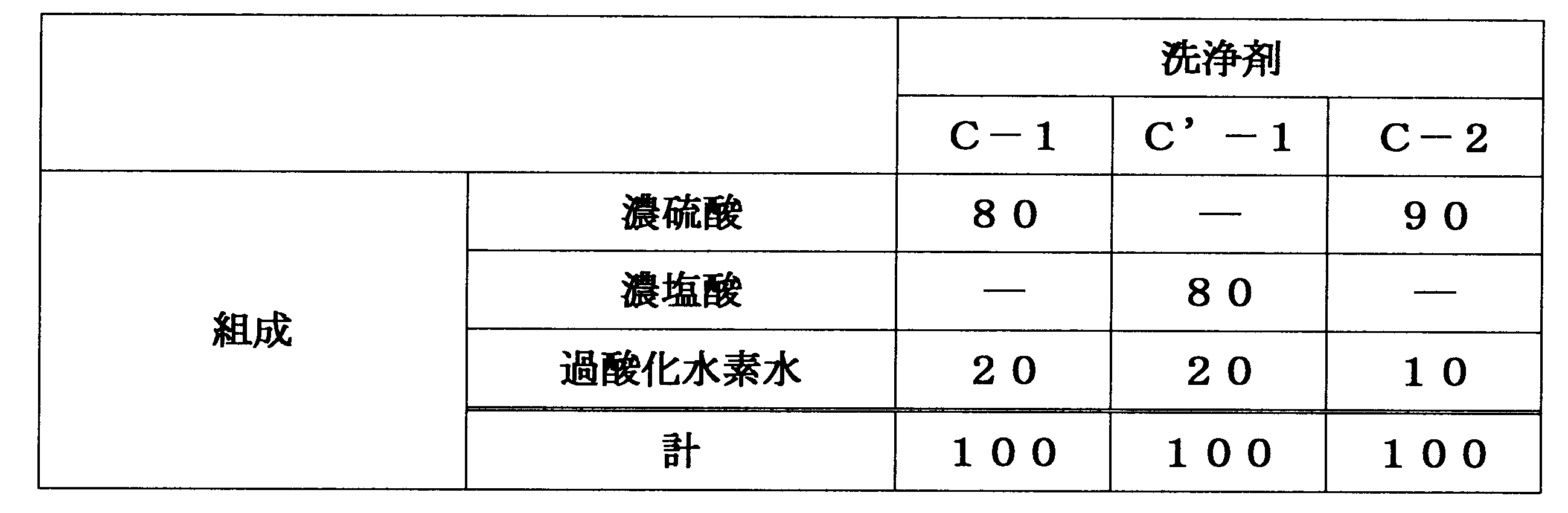
(調製例5)洗浄剤C-1(洗浄剤(C)に相当)の調製
表3の組成(ただし、組成中の硫酸の純分は77質量%であり、過酸化水素の純分は6質量%である。)に従い、各原料を混合して、洗浄剤C-1を得た。
表3の組成(ただし、組成中の硫酸の純分は77質量%であり、過酸化水素の純分は6質量%である。)に従い、各原料を混合して、洗浄剤C-1を得た。
(調製例6)洗浄剤C’-1(洗浄剤(C)の比較品)の調製
表3の組成(ただし、組成中の塩酸の純分は28質量%であり、過酸化水素の純分は6質量%である。)に従い、各原料を混合して、洗浄剤C’-1を得た。
(調製例7)洗浄剤C-2(洗浄剤(C)に相当)の調製
表3の組成(ただし、組成中の硫酸の純分は86質量%であり、過酸化水素の純分は3質量%である。)に従い、各原料を混合して、洗浄剤C-2を得た。
表3の組成(ただし、組成中の塩酸の純分は28質量%であり、過酸化水素の純分は6質量%である。)に従い、各原料を混合して、洗浄剤C’-1を得た。
(調製例7)洗浄剤C-2(洗浄剤(C)に相当)の調製
表3の組成(ただし、組成中の硫酸の純分は86質量%であり、過酸化水素の純分は3質量%である。)に従い、各原料を混合して、洗浄剤C-2を得た。

(清浄度の評価方法)
各例の洗浄方法で洗浄された半導体基板を、クラス1000の環境下(基板表面の1立方フィート当たりに、0.5μm以上の大きさの粒子が1000個以下になるように管理されたクリーンルーム内)で、回転数1000rpmで回転させ、乾燥した(スピン乾燥)。ウェハ表面検査装置Candela CS10(KLA Tencor社製)を用い、クラス1000の環境下で、乾燥後の半導体基板の表面に残留している0.5μm以上のパーティクルの数(残留パーティクル数)を測定した。測定された残留パーティクル数を下記評価基準に分類して、清浄度を評価した。
各例の洗浄方法で洗浄された半導体基板を、クラス1000の環境下(基板表面の1立方フィート当たりに、0.5μm以上の大きさの粒子が1000個以下になるように管理されたクリーンルーム内)で、回転数1000rpmで回転させ、乾燥した(スピン乾燥)。ウェハ表面検査装置Candela CS10(KLA Tencor社製)を用い、クラス1000の環境下で、乾燥後の半導体基板の表面に残留している0.5μm以上のパーティクルの数(残留パーティクル数)を測定した。測定された残留パーティクル数を下記評価基準に分類して、清浄度を評価した。
<評価基準>
1点:残留パーティクル数が10000個/枚超。
2点:残留パーティクル数が1000個/枚超、10000個/枚以下。
3点:残留パーティクル数が500個/枚超、1000個/枚以下。
4点:残留パーティクル数が200個/枚超、500個/枚以下。
5点:残留パーティクル数が100個/枚超、200個/枚以下。
6点:残留パーティクル数が100個/枚以下。
1点:残留パーティクル数が10000個/枚超。
2点:残留パーティクル数が1000個/枚超、10000個/枚以下。
3点:残留パーティクル数が500個/枚超、1000個/枚以下。
4点:残留パーティクル数が200個/枚超、500個/枚以下。
5点:残留パーティクル数が100個/枚超、200個/枚以下。
6点:残留パーティクル数が100個/枚以下。
(半導体基板Iの作製)
サファイア塊をスライスして原板を得た。得られた原板をワックス(ホットメルト系接着剤)で研磨治具に固定し(ワックス固定法)、研磨材であるコロイダルシリカを用いて研磨処理を施して、直径4インチ(10cm)の半導体基板Iを得た。研磨処理には、研磨機として片面ポリッシングマシンを用いた。
サファイア塊をスライスして原板を得た。得られた原板をワックス(ホットメルト系接着剤)で研磨治具に固定し(ワックス固定法)、研磨材であるコロイダルシリカを用いて研磨処理を施して、直径4インチ(10cm)の半導体基板Iを得た。研磨処理には、研磨機として片面ポリッシングマシンを用いた。
(半導体基板IIの作製)
サファイア塊をスライスして原板を得た。得られた原板をセラミック製のテンプレートに嵌め込んで固定し(嵌合固定法)、研磨材であるコロイダルシリカを用いて研磨処理を施して、直径4インチ(10cm)の半導体基板IIを得た。研磨処理には、研磨機として片面ポリッシングマシンを用いた。
サファイア塊をスライスして原板を得た。得られた原板をセラミック製のテンプレートに嵌め込んで固定し(嵌合固定法)、研磨材であるコロイダルシリカを用いて研磨処理を施して、直径4インチ(10cm)の半導体基板IIを得た。研磨処理には、研磨機として片面ポリッシングマシンを用いた。
(実施例1、4、比較例11~12、15~16)
表4及び表5に示す種類の半導体基板を、表4及び表5中の「第一の洗浄操作の洗浄剤」10Lに浸漬し、洗浄剤(50℃)に超音波を10分間印加(周波数36kHz)した(第一の洗浄操作)。
表4及び表5中の「第二の洗浄操作の洗浄剤」10Lを130℃とし、これに第一の洗浄操作で洗浄された半導体基板を10分間浸漬した(第二の洗浄操作)。
第二の洗浄操作で洗浄された半導体基板について、清浄度を評価し、その結果を表4及び表5に示す。
表4及び表5に示す種類の半導体基板を、表4及び表5中の「第一の洗浄操作の洗浄剤」10Lに浸漬し、洗浄剤(50℃)に超音波を10分間印加(周波数36kHz)した(第一の洗浄操作)。
表4及び表5中の「第二の洗浄操作の洗浄剤」10Lを130℃とし、これに第一の洗浄操作で洗浄された半導体基板を10分間浸漬した(第二の洗浄操作)。
第二の洗浄操作で洗浄された半導体基板について、清浄度を評価し、その結果を表4及び表5に示す。
(実施例2~3、比較例13~14、17~18)
表4及び表5中の「第一の洗浄操作の洗浄剤」を純水で20倍に希釈して洗浄液とし、この洗浄液10L(50℃)を用いて第一の洗浄操作を行った以外は、実施例1と同様にして半導体基板を洗浄した。洗浄された半導体基板について、清浄度を評価し、その結果を表4及び表5に示す。
表4及び表5中の「第一の洗浄操作の洗浄剤」を純水で20倍に希釈して洗浄液とし、この洗浄液10L(50℃)を用いて第一の洗浄操作を行った以外は、実施例1と同様にして半導体基板を洗浄した。洗浄された半導体基板について、清浄度を評価し、その結果を表4及び表5に示す。
(実施例5~6)
実施例1と同様にして、第一の洗浄操作と第二の洗浄操作とにより表4に示す種類の半導体基板を洗浄した。
第二の洗浄操作で洗浄された半導体基板を表4中の「第三の洗浄操作の洗浄剤」10Lに浸漬し、洗浄液(50℃)に超音波を10分間印加(周波数36kHz)した(第三の洗浄操作)。
表4中の「第四の洗浄操作の洗浄剤」10Lを130℃とし、これに第三の洗浄操作で洗浄された半導体基板を10分間浸漬した(第四の洗浄操作)。
第四の洗浄操作で洗浄された半導体基板について、清浄度を評価し、その結果を表4に示す。
実施例1と同様にして、第一の洗浄操作と第二の洗浄操作とにより表4に示す種類の半導体基板を洗浄した。
第二の洗浄操作で洗浄された半導体基板を表4中の「第三の洗浄操作の洗浄剤」10Lに浸漬し、洗浄液(50℃)に超音波を10分間印加(周波数36kHz)した(第三の洗浄操作)。
表4中の「第四の洗浄操作の洗浄剤」10Lを130℃とし、これに第三の洗浄操作で洗浄された半導体基板を10分間浸漬した(第四の洗浄操作)。
第四の洗浄操作で洗浄された半導体基板について、清浄度を評価し、その結果を表4に示す。
(実施例7~8)
実施例2と同様にして、第一の洗浄操作と第二の洗浄操作とにより表4に示す種類の半導体基板を洗浄した。
表4中の「第三の洗浄操作の洗浄剤」を純水で20倍に希釈して洗浄液とし、この洗浄液10L(50℃)に第二の洗浄操作で洗浄された半導体基板を浸漬し、洗浄液に超音波を10分間印加(周波数36kHz)した(第三の洗浄操作)。
表4中の「第四の洗浄操作の洗浄剤」10Lを130℃とし、これに第三の洗浄操作で洗浄された半導体基板を10分間浸漬した(第四の洗浄操作)。
第四の洗浄操作で洗浄された半導体基板について、清浄度を評価し、その結果を表4に示す。
実施例2と同様にして、第一の洗浄操作と第二の洗浄操作とにより表4に示す種類の半導体基板を洗浄した。
表4中の「第三の洗浄操作の洗浄剤」を純水で20倍に希釈して洗浄液とし、この洗浄液10L(50℃)に第二の洗浄操作で洗浄された半導体基板を浸漬し、洗浄液に超音波を10分間印加(周波数36kHz)した(第三の洗浄操作)。
表4中の「第四の洗浄操作の洗浄剤」10Lを130℃とし、これに第三の洗浄操作で洗浄された半導体基板を10分間浸漬した(第四の洗浄操作)。
第四の洗浄操作で洗浄された半導体基板について、清浄度を評価し、その結果を表4に示す。
(実施例9~10)
表4中の「第三の洗浄操作の洗浄剤」を純水で20倍に希釈して洗浄液とし、この洗浄液10L(50℃)を用いて第三の洗浄操作を行った以外は、実施例5と同様にして半導体基板を洗浄した。洗浄された半導体基板について、清浄度を評価し、その結果を表4に示す。
表4中の「第三の洗浄操作の洗浄剤」を純水で20倍に希釈して洗浄液とし、この洗浄液10L(50℃)を用いて第三の洗浄操作を行った以外は、実施例5と同様にして半導体基板を洗浄した。洗浄された半導体基板について、清浄度を評価し、その結果を表4に示す。
(実施例11~12)
表4中の「第三の洗浄操作の洗浄剤」を希釈せずに洗浄液とし、この洗浄液10L(50℃)を用いて第三の洗浄操作を行った以外は、実施例7と同様にして半導体基板を洗浄した。洗浄された半導体基板について、清浄度を評価し、その結果を表4に示す。
(実施例13~14)
洗浄剤C-1を洗浄剤C-2に変更したこと以外は、実施例9~10と同様にして半導体基板を洗浄した。洗浄された半導体基板について、清浄度を評価し、その結果を表4に示す。
(実施例15)
洗浄剤C-1を洗浄剤C-2に変更したこと以外は、実施例7と同様にして半導体基板を洗浄した。洗浄された半導体基板について、清浄度を評価し、その結果を表4に示す。
表4中の「第三の洗浄操作の洗浄剤」を希釈せずに洗浄液とし、この洗浄液10L(50℃)を用いて第三の洗浄操作を行った以外は、実施例7と同様にして半導体基板を洗浄した。洗浄された半導体基板について、清浄度を評価し、その結果を表4に示す。
(実施例13~14)
洗浄剤C-1を洗浄剤C-2に変更したこと以外は、実施例9~10と同様にして半導体基板を洗浄した。洗浄された半導体基板について、清浄度を評価し、その結果を表4に示す。
(実施例15)
洗浄剤C-1を洗浄剤C-2に変更したこと以外は、実施例7と同様にして半導体基板を洗浄した。洗浄された半導体基板について、清浄度を評価し、その結果を表4に示す。
(比較例1~2)
第二の洗浄操作を行わなかった以外は、実施例1と同様にして半導体基板を洗浄した。
洗浄された半導体基板について、清浄度を評価し、その結果を表5に示す。
第二の洗浄操作を行わなかった以外は、実施例1と同様にして半導体基板を洗浄した。
洗浄された半導体基板について、清浄度を評価し、その結果を表5に示す。
(比較例3~4)
第二の洗浄操作を行わなかった以外は、実施例2と同様にして半導体基板を洗浄した。
洗浄された半導体基板について、清浄度を評価し、その結果を表5に示す。
第二の洗浄操作を行わなかった以外は、実施例2と同様にして半導体基板を洗浄した。
洗浄された半導体基板について、清浄度を評価し、その結果を表5に示す。
(比較例5~6)
表5中の「第一の洗浄操作の洗浄剤」10Lを130℃とし、これに表5に示す種類の半導体基板を10分間浸漬した。即ち、比較例5~6においては、実施例1における第一の洗浄操作が省略された。洗浄された半導体基板について、清浄度を評価し、その結果を表5に示す。
表5中の「第一の洗浄操作の洗浄剤」10Lを130℃とし、これに表5に示す種類の半導体基板を10分間浸漬した。即ち、比較例5~6においては、実施例1における第一の洗浄操作が省略された。洗浄された半導体基板について、清浄度を評価し、その結果を表5に示す。
(比較例7~8)
表5中の「第一の洗浄操作の洗浄剤」10Lを130℃とし、表5に示す種類の半導体基板を10分間浸漬した(第一の洗浄操作)。
第一の洗浄操作で洗浄された半導体基板を表5中の「第二の洗浄操作の洗浄剤」10Lに浸漬し、洗浄剤(50℃)に超音波を10分間印加(周波数36kHz)した(第二の洗浄操作)。
第二の洗浄操作で洗浄された半導体基板について、清浄度を評価し、その結果を表4に示す。
表5中の「第一の洗浄操作の洗浄剤」10Lを130℃とし、表5に示す種類の半導体基板を10分間浸漬した(第一の洗浄操作)。
第一の洗浄操作で洗浄された半導体基板を表5中の「第二の洗浄操作の洗浄剤」10Lに浸漬し、洗浄剤(50℃)に超音波を10分間印加(周波数36kHz)した(第二の洗浄操作)。
第二の洗浄操作で洗浄された半導体基板について、清浄度を評価し、その結果を表4に示す。
(比較例9~10)
表5中の「第二の洗浄操作の洗浄剤」を純水で20倍に希釈して洗浄液とし、この洗浄液10Lを用いて第二の洗浄操作を行った以外は、比較例7と同様にして半導体基板を洗浄した。洗浄された半導体基板について、清浄度を評価し、その結果を表5に示す。
表5中の「第二の洗浄操作の洗浄剤」を純水で20倍に希釈して洗浄液とし、この洗浄液10Lを用いて第二の洗浄操作を行った以外は、比較例7と同様にして半導体基板を洗浄した。洗浄された半導体基板について、清浄度を評価し、その結果を表5に示す。
(比較例19)
半導体基板Iを下記の方法により洗浄した。
まず、アセトン(ELグレード試薬、関東化学株式会社製)10Lに半導体基板を浸漬し、25℃でアセトンに超音波を10分間印加した(第一の溶剤洗浄)。
第一の溶剤洗浄で洗浄された半導体基板をイソプロピルアルコール(ELグレード試薬、関東化学株式会社製)10Lに浸漬し、25℃でイソプロピルアルコールに超音波を5分間印加した(第二の溶剤洗浄)。
第二の溶剤洗浄で洗浄された半導体基板を濃硫酸(ELグレード試薬、関東化学株式会社製):過酸化水素水(ELグレード試薬、関東化学株式会社製)=4:1の混合液10L(120℃)に10分間浸漬した(硫酸過酸化水素水(SPM)洗浄)。
SPM洗浄で洗浄された半導体基板をアンモニア水(ELグレード試薬、関東化学株式会社製):過酸化水素水(ELグレード試薬、関東化学株式会社製):水=1:1:5の混合液10L(80℃)に5分間浸漬した(アンモニア過酸化水素水(APM)洗浄)。
APM洗浄で洗浄された半導体基板をフッ酸(ELグレード試薬、関東化学株式会社製):水=1:5の混合液10L(25℃)に5分間浸漬した(希フッ酸(DHF)洗浄)。
DHF洗浄で洗浄された半導体基板を濃塩酸(ELグレード試薬、関東化学株式会社製):過酸化水素水(ELグレード試薬、関東化学株式会社製):水=1:1:5の混合液10L(25℃)に5分間浸漬した(塩酸過酸化水素水(HPM)洗浄)。
HPM洗浄を終えた半導体基板の清浄度を評価したところ、評価は2点(残留パーティクル数が2000個)であった。
半導体基板Iを下記の方法により洗浄した。
まず、アセトン(ELグレード試薬、関東化学株式会社製)10Lに半導体基板を浸漬し、25℃でアセトンに超音波を10分間印加した(第一の溶剤洗浄)。
第一の溶剤洗浄で洗浄された半導体基板をイソプロピルアルコール(ELグレード試薬、関東化学株式会社製)10Lに浸漬し、25℃でイソプロピルアルコールに超音波を5分間印加した(第二の溶剤洗浄)。
第二の溶剤洗浄で洗浄された半導体基板を濃硫酸(ELグレード試薬、関東化学株式会社製):過酸化水素水(ELグレード試薬、関東化学株式会社製)=4:1の混合液10L(120℃)に10分間浸漬した(硫酸過酸化水素水(SPM)洗浄)。
SPM洗浄で洗浄された半導体基板をアンモニア水(ELグレード試薬、関東化学株式会社製):過酸化水素水(ELグレード試薬、関東化学株式会社製):水=1:1:5の混合液10L(80℃)に5分間浸漬した(アンモニア過酸化水素水(APM)洗浄)。
APM洗浄で洗浄された半導体基板をフッ酸(ELグレード試薬、関東化学株式会社製):水=1:5の混合液10L(25℃)に5分間浸漬した(希フッ酸(DHF)洗浄)。
DHF洗浄で洗浄された半導体基板を濃塩酸(ELグレード試薬、関東化学株式会社製):過酸化水素水(ELグレード試薬、関東化学株式会社製):水=1:1:5の混合液10L(25℃)に5分間浸漬した(塩酸過酸化水素水(HPM)洗浄)。
HPM洗浄を終えた半導体基板の清浄度を評価したところ、評価は2点(残留パーティクル数が2000個)であった。
(比較例20)
半導体基板Iを半導体基板IIに換えた以外は、比較例19と同様にして、半導体基板を洗浄した。洗浄された半導体基板の清浄度を評価したところ、評価は2点(残留パーティクル数が3500個)であった。
半導体基板Iを半導体基板IIに換えた以外は、比較例19と同様にして、半導体基板を洗浄した。洗浄された半導体基板の清浄度を評価したところ、評価は2点(残留パーティクル数が3500個)であった。
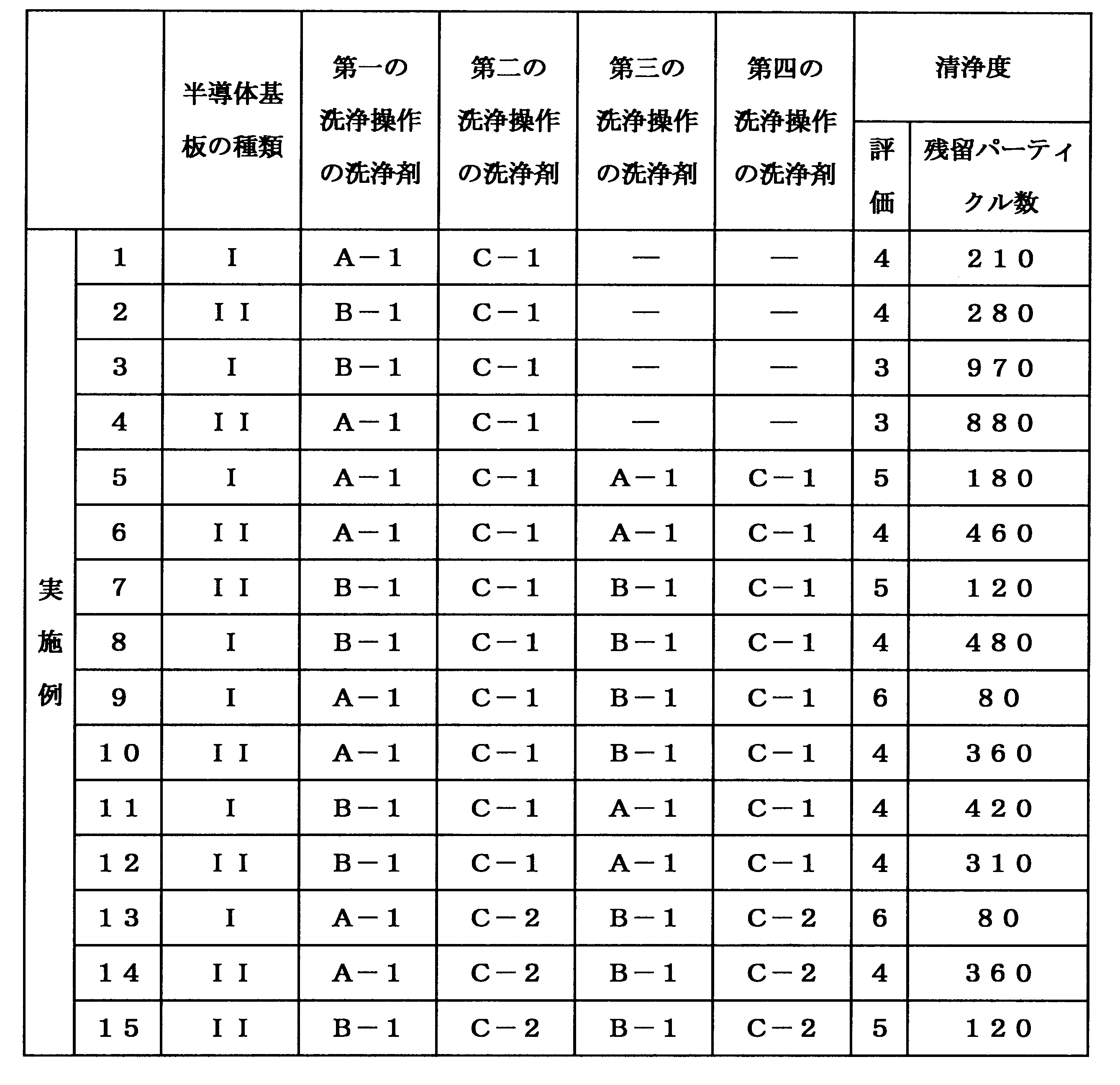
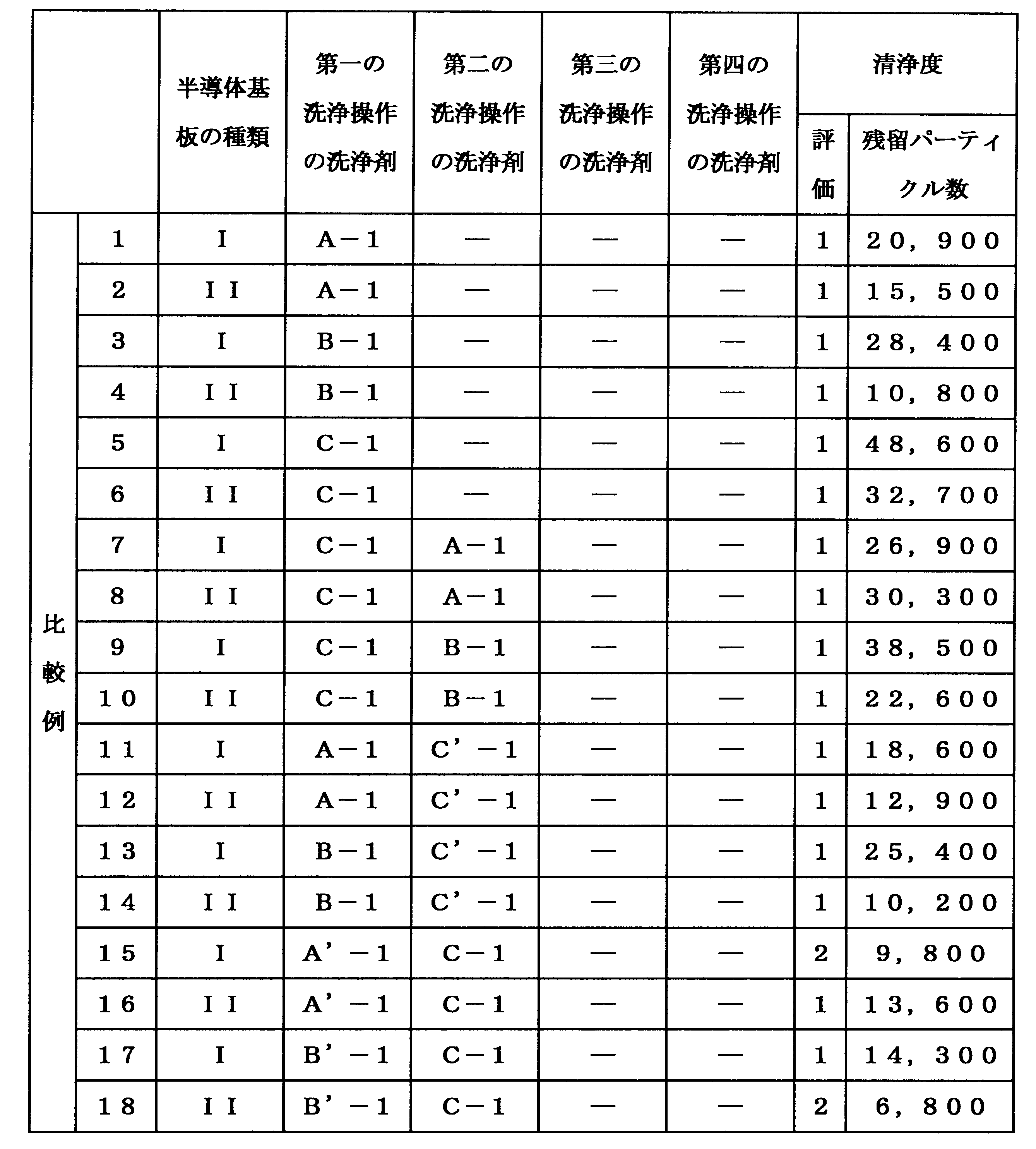
表4に示すように、本発明を適用した実施例1~12は、清浄度の評価が3点以上であった。中でも、第三~第四の洗浄操作を備える実施例5~12は、第三~第四の洗浄操作を備えない実施例1~4に比べて、総じて清浄度を高められた。
第一の洗浄操作に洗浄剤A-1を用い、第三の洗浄操作に洗浄剤B-1を用いた実施例9は、実施例1及び5よりも半導体基板Iの清浄度をより高められた。
第一の洗浄操作及び第三の洗浄操作に洗浄剤B-1を用いた実施例7は、実施例2及び12よりも半導体基板IIの清浄度をより高められた。
表5に示すように、洗浄剤A-1、洗浄剤B-1又は洗浄剤C-1で洗浄する操作のみを備える比較例1~6は、清浄度の評価が1点であった。
第一の洗浄操作に洗浄剤C-1を用い、第二の洗浄操作に洗浄剤A-1又は洗浄剤B-1を用いた比較例7~10は、清浄度の評価が1点であった。
第二の洗浄操作に洗浄剤C’-1を用いた比較例11~14、第一の洗浄操作に洗浄剤A’-1又は洗浄剤B’-1を用いた比較例15~18は、清浄度の評価が2点以下であった。
比較例19~20は、半導体基板に対する従来の洗浄方法であり、溶剤洗浄(第一及び第二の溶剤洗浄)とRCA洗浄(SPM洗浄~HPM洗浄)とを組み合わせたものである。この比較例19~20は、清浄度の評価が2点であった。
これらの結果から、本発明を適用することで、半導体基板の清浄度をより高められることが判った。
第一の洗浄操作に洗浄剤A-1を用い、第三の洗浄操作に洗浄剤B-1を用いた実施例9は、実施例1及び5よりも半導体基板Iの清浄度をより高められた。
第一の洗浄操作及び第三の洗浄操作に洗浄剤B-1を用いた実施例7は、実施例2及び12よりも半導体基板IIの清浄度をより高められた。
表5に示すように、洗浄剤A-1、洗浄剤B-1又は洗浄剤C-1で洗浄する操作のみを備える比較例1~6は、清浄度の評価が1点であった。
第一の洗浄操作に洗浄剤C-1を用い、第二の洗浄操作に洗浄剤A-1又は洗浄剤B-1を用いた比較例7~10は、清浄度の評価が1点であった。
第二の洗浄操作に洗浄剤C’-1を用いた比較例11~14、第一の洗浄操作に洗浄剤A’-1又は洗浄剤B’-1を用いた比較例15~18は、清浄度の評価が2点以下であった。
比較例19~20は、半導体基板に対する従来の洗浄方法であり、溶剤洗浄(第一及び第二の溶剤洗浄)とRCA洗浄(SPM洗浄~HPM洗浄)とを組み合わせたものである。この比較例19~20は、清浄度の評価が2点であった。
これらの結果から、本発明を適用することで、半導体基板の清浄度をより高められることが判った。
Claims (6)
- 下記洗浄剤(A)又は下記洗浄剤(B)を用いて、研磨処理が施された半導体基板を洗浄する第一の洗浄操作と、
前記第一の洗浄操作の後、下記洗浄剤(C)を用いて、前記半導体基板を洗浄する第二の洗浄操作とを備える半導体基板の洗浄方法。
洗浄剤(A):炭化水素化合物と、グリコールエーテルと、界面活性剤とを含有する液体洗浄剤。
洗浄剤(B):アルカリ金属の水酸化物と、ヒドロキシカルボン酸及びその塩から選択される1種以上と、1-ヒドロキシエタン-1,1-ジホスホン酸及びその塩から選択される1種以上とを含有する液体洗浄剤。
洗浄剤(C):硫酸と過酸化水素とを含有し、硫酸濃度が50質量%以上である液体洗浄剤。 - 前記第二の洗浄操作の後、新たに前記洗浄剤(A)又は前記洗浄剤(B)を用いて、前記半導体基板を洗浄する第三の洗浄操作と、
前記第三の洗浄操作の後、新たに前記洗浄剤(C)を用いて、前記半導体基板を洗浄する第四の洗浄操作とをさらに備える請求項1に記載の半導体基板の洗浄方法。 - 前記第一の洗浄操作には、前記洗浄剤(A)を用い、前記第三の洗浄操作には、前記洗浄剤(B)を用いる請求項2に記載の半導体基板の洗浄方法。
- 前記第一の洗浄操作には、前記洗浄剤(B)を用い、前記第三の洗浄操作には、前記洗浄剤(B)を用いる請求項2に記載の半導体基板の洗浄方法。
- 前記半導体基板は、単結晶サファイア基板である請求項1に記載の半導体基板の洗浄方法。
- 請求項1~5のいずれか1項に記載の半導体基板の洗浄方法で半導体基板を洗浄する洗浄工程を備える半導体基板の製造方法。
Priority Applications (1)
| Application Number | Priority Date | Filing Date | Title |
|---|---|---|---|
| JP2014547055A JPWO2014077370A1 (ja) | 2012-11-16 | 2013-11-15 | 半導体基板の洗浄方法、及び半導体基板の製造方法 |
Applications Claiming Priority (2)
| Application Number | Priority Date | Filing Date | Title |
|---|---|---|---|
| JP2012251819 | 2012-11-16 | ||
| JP2012-251819 | 2012-11-16 |
Publications (1)
| Publication Number | Publication Date |
|---|---|
| WO2014077370A1 true WO2014077370A1 (ja) | 2014-05-22 |
Family
ID=50731279
Family Applications (1)
| Application Number | Title | Priority Date | Filing Date |
|---|---|---|---|
| PCT/JP2013/080939 Ceased WO2014077370A1 (ja) | 2012-11-16 | 2013-11-15 | 半導体基板の洗浄方法、及び半導体基板の製造方法 |
Country Status (3)
| Country | Link |
|---|---|
| JP (1) | JPWO2014077370A1 (ja) |
| TW (1) | TW201439312A (ja) |
| WO (1) | WO2014077370A1 (ja) |
Cited By (2)
| Publication number | Priority date | Publication date | Assignee | Title |
|---|---|---|---|---|
| WO2022070969A1 (ja) * | 2020-09-30 | 2022-04-07 | 株式会社フジミインコーポレーテッド | 酸化ガリウム基板用洗浄剤 |
| WO2026018713A1 (ja) * | 2024-07-16 | 2026-01-22 | 花王株式会社 | フラックス残渣除去用洗浄剤組成物 |
Citations (6)
| Publication number | Priority date | Publication date | Assignee | Title |
|---|---|---|---|---|
| JP2008159789A (ja) * | 2006-12-22 | 2008-07-10 | Renesas Technology Corp | 半導体装置の製造方法 |
| JP2009021471A (ja) * | 2007-07-13 | 2009-01-29 | Renesas Technology Corp | 半導体装置の製造方法 |
| WO2009102004A1 (ja) * | 2008-02-15 | 2009-08-20 | Lion Corporation | 洗浄剤組成物および電子デバイス用基板の洗浄方法 |
| JP2010109329A (ja) * | 2008-10-02 | 2010-05-13 | Lion Corp | 電子デバイス基板用洗浄剤組成物、および電子デバイス基板の洗浄方法 |
| JP4887266B2 (ja) * | 2007-10-15 | 2012-02-29 | 株式会社荏原製作所 | 平坦化方法 |
| JP2012104371A (ja) * | 2010-11-10 | 2012-05-31 | Hitachi Cable Ltd | 発泡絶縁電線及びその製造方法 |
-
2013
- 2013-11-15 TW TW102141807A patent/TW201439312A/zh unknown
- 2013-11-15 JP JP2014547055A patent/JPWO2014077370A1/ja active Pending
- 2013-11-15 WO PCT/JP2013/080939 patent/WO2014077370A1/ja not_active Ceased
Patent Citations (6)
| Publication number | Priority date | Publication date | Assignee | Title |
|---|---|---|---|---|
| JP2008159789A (ja) * | 2006-12-22 | 2008-07-10 | Renesas Technology Corp | 半導体装置の製造方法 |
| JP2009021471A (ja) * | 2007-07-13 | 2009-01-29 | Renesas Technology Corp | 半導体装置の製造方法 |
| JP4887266B2 (ja) * | 2007-10-15 | 2012-02-29 | 株式会社荏原製作所 | 平坦化方法 |
| WO2009102004A1 (ja) * | 2008-02-15 | 2009-08-20 | Lion Corporation | 洗浄剤組成物および電子デバイス用基板の洗浄方法 |
| JP2010109329A (ja) * | 2008-10-02 | 2010-05-13 | Lion Corp | 電子デバイス基板用洗浄剤組成物、および電子デバイス基板の洗浄方法 |
| JP2012104371A (ja) * | 2010-11-10 | 2012-05-31 | Hitachi Cable Ltd | 発泡絶縁電線及びその製造方法 |
Cited By (2)
| Publication number | Priority date | Publication date | Assignee | Title |
|---|---|---|---|---|
| WO2022070969A1 (ja) * | 2020-09-30 | 2022-04-07 | 株式会社フジミインコーポレーテッド | 酸化ガリウム基板用洗浄剤 |
| WO2026018713A1 (ja) * | 2024-07-16 | 2026-01-22 | 花王株式会社 | フラックス残渣除去用洗浄剤組成物 |
Also Published As
| Publication number | Publication date |
|---|---|
| TW201439312A (zh) | 2014-10-16 |
| JPWO2014077370A1 (ja) | 2017-01-05 |
Similar Documents
| Publication | Publication Date | Title |
|---|---|---|
| JP5155121B2 (ja) | 電子材料用洗浄剤及び洗浄方法 | |
| CN101942667B (zh) | 用于cmp后清洗的配方和方法 | |
| KR101520917B1 (ko) | 웨이퍼의 표면 처리용 텍스쳐링 및 세정제 및 그것의 사용 | |
| CN1155055C (zh) | 清洗剂以及使用它的清洗方法 | |
| CN1639846A (zh) | 半导体器件用基板的清洗液及清洗方法 | |
| CN1918698A (zh) | 半导体装置用基板的洗涤液及洗涤方法 | |
| JP4207976B2 (ja) | 化合物半導体基板の表面処理方法、および化合物半導体結晶の製造方法 | |
| KR101956388B1 (ko) | 사파이어 웨이퍼 세정제 조성물 | |
| JP3624809B2 (ja) | 洗浄剤組成物、洗浄方法及びその用途 | |
| WO2018216203A1 (ja) | GaAs基板およびその製造方法 | |
| JP2008135576A (ja) | エレクトロニクス材料用洗浄剤 | |
| CN102560519B (zh) | 一种金属防腐清洗液 | |
| JP2013010888A (ja) | 半導体基板用洗浄剤組成物 | |
| WO2014077370A1 (ja) | 半導体基板の洗浄方法、及び半導体基板の製造方法 | |
| JP2003068696A (ja) | 基板表面洗浄方法 | |
| JP5324242B2 (ja) | 電子材料用洗浄剤及び洗浄方法 | |
| JP2003109930A (ja) | 半導体デバイス用基板の洗浄液及び洗浄方法 | |
| JP2003088817A (ja) | 基板表面洗浄方法 | |
| JP2014172964A (ja) | 洗浄剤組成物 | |
| JP6533030B2 (ja) | シリコンウエハ用洗浄剤組成物 | |
| JP2003100671A (ja) | 半導体結晶ウェハの研磨方法及び半導体結晶ウェハ | |
| JP2009182225A (ja) | 半導体デバイス用洗浄剤及びそれを用いた半導体デバイスの洗浄方法 | |
| KR102635269B1 (ko) | 전자재료용의 세정제 조성물, 세정제 원액, 및 전자재료의 세정방법 | |
| JP2003313584A (ja) | 洗浄剤組成物 | |
| JP4874772B2 (ja) | スライスしたシリコンウエハ又はインゴット用洗浄剤組成物 |
Legal Events
| Date | Code | Title | Description |
|---|---|---|---|
| 121 | Ep: the epo has been informed by wipo that ep was designated in this application |
Ref document number: 13855109 Country of ref document: EP Kind code of ref document: A1 |
|
| ENP | Entry into the national phase |
Ref document number: 2014547055 Country of ref document: JP Kind code of ref document: A |
|
| NENP | Non-entry into the national phase |
Ref country code: DE |
|
| 122 | Ep: pct application non-entry in european phase |
Ref document number: 13855109 Country of ref document: EP Kind code of ref document: A1 |