WO2014073191A1 - 電子デバイスの製造方法および該製造方法に用いられる積層体 - Google Patents
電子デバイスの製造方法および該製造方法に用いられる積層体 Download PDFInfo
- Publication number
- WO2014073191A1 WO2014073191A1 PCT/JP2013/006487 JP2013006487W WO2014073191A1 WO 2014073191 A1 WO2014073191 A1 WO 2014073191A1 JP 2013006487 W JP2013006487 W JP 2013006487W WO 2014073191 A1 WO2014073191 A1 WO 2014073191A1
- Authority
- WO
- WIPO (PCT)
- Prior art keywords
- flexible substrate
- adhesive
- light
- electronic device
- layer
- Prior art date
- Legal status (The legal status is an assumption and is not a legal conclusion. Google has not performed a legal analysis and makes no representation as to the accuracy of the status listed.)
- Ceased
Links
Images






Classifications
-
- H—ELECTRICITY
- H10—SEMICONDUCTOR DEVICES; ELECTRIC SOLID-STATE DEVICES NOT OTHERWISE PROVIDED FOR
- H10D—INORGANIC ELECTRIC SEMICONDUCTOR DEVICES
- H10D86/00—Integrated devices formed in or on insulating or conducting substrates, e.g. formed in silicon-on-insulator [SOI] substrates or on stainless steel or glass substrates
- H10D86/40—Integrated devices formed in or on insulating or conducting substrates, e.g. formed in silicon-on-insulator [SOI] substrates or on stainless steel or glass substrates characterised by multiple TFTs
- H10D86/411—Integrated devices formed in or on insulating or conducting substrates, e.g. formed in silicon-on-insulator [SOI] substrates or on stainless steel or glass substrates characterised by multiple TFTs characterised by materials, geometry or structure of the substrates
-
- H—ELECTRICITY
- H10—SEMICONDUCTOR DEVICES; ELECTRIC SOLID-STATE DEVICES NOT OTHERWISE PROVIDED FOR
- H10D—INORGANIC ELECTRIC SEMICONDUCTOR DEVICES
- H10D86/00—Integrated devices formed in or on insulating or conducting substrates, e.g. formed in silicon-on-insulator [SOI] substrates or on stainless steel or glass substrates
- H10D86/40—Integrated devices formed in or on insulating or conducting substrates, e.g. formed in silicon-on-insulator [SOI] substrates or on stainless steel or glass substrates characterised by multiple TFTs
- H10D86/60—Integrated devices formed in or on insulating or conducting substrates, e.g. formed in silicon-on-insulator [SOI] substrates or on stainless steel or glass substrates characterised by multiple TFTs wherein the TFTs are in active matrices
-
- H—ELECTRICITY
- H10—SEMICONDUCTOR DEVICES; ELECTRIC SOLID-STATE DEVICES NOT OTHERWISE PROVIDED FOR
- H10F—INORGANIC SEMICONDUCTOR DEVICES SENSITIVE TO INFRARED RADIATION, LIGHT, ELECTROMAGNETIC RADIATION OF SHORTER WAVELENGTH OR CORPUSCULAR RADIATION
- H10F39/00—Integrated devices, or assemblies of multiple devices, comprising at least one element covered by group H10F30/00, e.g. radiation detectors comprising photodiode arrays
- H10F39/10—Integrated devices
- H10F39/12—Image sensors
- H10F39/191—Photoconductor image sensors
-
- H—ELECTRICITY
- H10—SEMICONDUCTOR DEVICES; ELECTRIC SOLID-STATE DEVICES NOT OTHERWISE PROVIDED FOR
- H10F—INORGANIC SEMICONDUCTOR DEVICES SENSITIVE TO INFRARED RADIATION, LIGHT, ELECTROMAGNETIC RADIATION OF SHORTER WAVELENGTH OR CORPUSCULAR RADIATION
- H10F77/00—Constructional details of devices covered by this subclass
- H10F77/10—Semiconductor bodies
- H10F77/16—Material structures, e.g. crystalline structures, film structures or crystal plane orientations
- H10F77/169—Thin semiconductor films on metallic or insulating substrates
- H10F77/1698—Thin semiconductor films on metallic or insulating substrates the metallic or insulating substrates being flexible
-
- H—ELECTRICITY
- H10—SEMICONDUCTOR DEVICES; ELECTRIC SOLID-STATE DEVICES NOT OTHERWISE PROVIDED FOR
- H10F—INORGANIC SEMICONDUCTOR DEVICES SENSITIVE TO INFRARED RADIATION, LIGHT, ELECTROMAGNETIC RADIATION OF SHORTER WAVELENGTH OR CORPUSCULAR RADIATION
- H10F77/00—Constructional details of devices covered by this subclass
- H10F77/10—Semiconductor bodies
- H10F77/16—Material structures, e.g. crystalline structures, film structures or crystal plane orientations
- H10F77/169—Thin semiconductor films on metallic or insulating substrates
- H10F77/1698—Thin semiconductor films on metallic or insulating substrates the metallic or insulating substrates being flexible
- H10F77/1699—Thin semiconductor films on metallic or insulating substrates the metallic or insulating substrates being flexible the films including Group I-III-VI materials, e.g. CIS or CIGS on metal foils or polymer foils
-
- H—ELECTRICITY
- H10—SEMICONDUCTOR DEVICES; ELECTRIC SOLID-STATE DEVICES NOT OTHERWISE PROVIDED FOR
- H10K—ORGANIC ELECTRIC SOLID-STATE DEVICES
- H10K71/00—Manufacture or treatment specially adapted for the organic devices covered by this subclass
- H10K71/80—Manufacture or treatment specially adapted for the organic devices covered by this subclass using temporary substrates
-
- H—ELECTRICITY
- H10—SEMICONDUCTOR DEVICES; ELECTRIC SOLID-STATE DEVICES NOT OTHERWISE PROVIDED FOR
- H10K—ORGANIC ELECTRIC SOLID-STATE DEVICES
- H10K59/00—Integrated devices, or assemblies of multiple devices, comprising at least one organic light-emitting element covered by group H10K50/00
- H10K59/10—OLED displays
- H10K59/12—Active-matrix OLED [AMOLED] displays
-
- Y—GENERAL TAGGING OF NEW TECHNOLOGICAL DEVELOPMENTS; GENERAL TAGGING OF CROSS-SECTIONAL TECHNOLOGIES SPANNING OVER SEVERAL SECTIONS OF THE IPC; TECHNICAL SUBJECTS COVERED BY FORMER USPC CROSS-REFERENCE ART COLLECTIONS [XRACs] AND DIGESTS
- Y02—TECHNOLOGIES OR APPLICATIONS FOR MITIGATION OR ADAPTATION AGAINST CLIMATE CHANGE
- Y02E—REDUCTION OF GREENHOUSE GAS [GHG] EMISSIONS, RELATED TO ENERGY GENERATION, TRANSMISSION OR DISTRIBUTION
- Y02E10/00—Energy generation through renewable energy sources
- Y02E10/50—Photovoltaic [PV] energy
- Y02E10/541—CuInSe2 material PV cells
-
- Y—GENERAL TAGGING OF NEW TECHNOLOGICAL DEVELOPMENTS; GENERAL TAGGING OF CROSS-SECTIONAL TECHNOLOGIES SPANNING OVER SEVERAL SECTIONS OF THE IPC; TECHNICAL SUBJECTS COVERED BY FORMER USPC CROSS-REFERENCE ART COLLECTIONS [XRACs] AND DIGESTS
- Y02—TECHNOLOGIES OR APPLICATIONS FOR MITIGATION OR ADAPTATION AGAINST CLIMATE CHANGE
- Y02P—CLIMATE CHANGE MITIGATION TECHNOLOGIES IN THE PRODUCTION OR PROCESSING OF GOODS
- Y02P70/00—Climate change mitigation technologies in the production process for final industrial or consumer products
- Y02P70/50—Manufacturing or production processes characterised by the final manufactured product
Definitions
- the present invention relates to a liquid crystal / organic EL display having a thin transistor, electronic paper, an X-ray sensor, and other electronic devices such as solar cells, in particular, a method for manufacturing a flexible electronic device, and a laminate used in the manufacturing method. It is about.
- a glass substrate is generally used as a substrate for forming a TFT, and the electronic device is made flexible, lightweight, and thin. In response to this requirement, the thickness of the glass substrate is being reduced.
- a resin film such as a plastic substrate or a thin metal substrate as a substrate on which a TFT is formed has been studied.
- metal substrates are useful as flexible substrates applicable to devices that require high-temperature processes because they have higher heat resistance than resin films and are not brittle (cracked) compared to thin glass substrates. It is.
- a functional element structure As a method for manufacturing an electronic device including a structure (hereinafter referred to as a functional element structure) including an element having a specific function such as a TFT on a flexible substrate, a functional element structure is directly formed on the flexible substrate. And a method of forming a functional element structure on a rigid substrate such as a glass substrate, and peeling the functional element structure from the substrate and transferring it onto a flexible substrate (indirect method or Transfer method).
- the indirect method or transfer method requires an additional process of peeling the functional element structure from the substrate and transferring it onto a flexible substrate, and the yield of the process is poor, so it is unsuitable for manufacturing. From the viewpoint of the above, it is preferable to produce by a direct method.
- the flexible substrate can be a roll-to-roll method in which a long substrate wound in a roll is continuously unwound and wound after at least one step, which is suitable for mass production.
- this system is a new manufacturing facility, and various roll-to-roll manufacturing apparatuses are required depending on electronic devices.
- a rigid substrate such as a conventional glass or silicon wafer
- an established batch type manufacturing apparatus is commercially available. By using this, it is possible to quickly manufacture electronic devices at low cost. Is possible.
- a flexible substrate is used in a state of being fixed to a rigid support body (hereinafter referred to as a support body) such as silicon or glass.
- a support body such as silicon or glass.
- the support when the support is peeled off from the flexible substrate after the functional element is manufactured, it is preferable that the support can be peeled off as easily as possible.
- the flexible substrate and the support are not peeled off during the functional element manufacturing process, but are pasted so that they can be easily peeled off after the end of the process.
- the support cannot be peeled off from the flexible substrate.
- the functional element manufacturing process for example, when amorphous silicon is formed by plasma CVD, it is necessary to raise the substrate temperature to a high temperature of about 350 ° C. At this time, the adhesive force is lowered and the support is flexible. There is a problem that the substrate peels off, or the curing of the adhesive proceeds at a high temperature, and the support cannot be peeled off from the flexible substrate after the process is completed.
- Patent Document 1 a resin film substrate or a thin metal substrate is bonded to a fixing support using an adhesive layer to form a light emitting element on the substrate, and laser light is irradiated from the fixed substrate side after the light emitting element is formed.
- a method for manufacturing a semiconductor device is disclosed in which a part or all of an adhesive layer is vaporized to separate a fixing support.
- the present invention has been made in view of the above circumstances, a method for manufacturing a high-performance flexible electronic device on a flexible metal substrate by a batch method, and a flexible substrate and a support suitable for the method. It is an object to provide a laminated laminate.
- a structure including an element having a specific function is formed on the porous anodized insulating film of a flexible substrate having a porous anodized insulating film on an aluminum material.
- An electronic device manufacturing method comprising: Prepare a flexible substrate and a light transmissive support, Adding an adhesive having heat resistance during the formation process of the structure including an element having a specific function in the pasting region to which the flexible substrate is pasted on the surface of the light-transmitting support; The surface opposite to the structure forming surface of the flexible substrate is attached to the light transmissive support via an adhesive, Forming a structure including an element having a specific function on the porous anodized insulating film; By irradiating a laser beam from the back side of the light transmissive support, the adhesive strength of the adhesive is reduced and the light transmissive support is peeled off from the flexible substrate.
- the light-transmitting support is peeled off by irradiating laser light from one end to the other end while two-dimensionally scanning, thereby reducing the adhesive strength of the adhesive. It is preferable to carry out gradually from one end side where irradiation is started.
- the one end and the other end of the pasting region may be spot-like or line-like depending on the mode of the laser light source.
- the irradiated laser beam is spot-shaped, two-dimensional scanning is performed by scanning in both directions of the main scanning direction and the sub-scanning direction.
- scanning is performed in a direction substantially orthogonal to the line.
- the difference in linear expansion coefficient between the flexible substrate and the light transmissive support is preferably 4 ppm / K or less.
- the linear expansion coefficient of the light-transmitting support is 3 to 9 ppm / K.
- the linear expansion coefficient of the light transmissive support is from 6 to It is preferably 13 ppm / K.
- the first laminate of the present invention can be suitably used for the method for producing an electronic device of the present invention,
- a laminated body in which a light-transmitting support having a linear expansion coefficient of 3 to 9 ppm / K and a flexible substrate having a porous anodized insulating film on an aluminum material are laminated via an adhesive.
- the adhesive strength of the adhesive is reduced, and the light transmissive support can be peeled from the flexible substrate.
- the second laminate of the present invention can also be suitably used in the method for producing an electronic device of the present invention,
- the light transmissive support having a linear expansion coefficient of 3 to 9 ppm / K is preferably non-alkali glass or borosilicate glass, and the light transmissive support having a linear expansion coefficient of 6 to 13 ppm / K is soda. Lime glass or white plate potash glass is preferred.
- the “light-transmitting support” means a support having a transmittance of 10% or more with respect to laser light irradiated from the back side of the light-transmitting transparent support.
- the term “heat-resistant adhesive” refers to the ability to maintain a state in which an object is bonded at that temperature, and “decreases the adhesive strength of the adhesive” It means that the adhesive strength of the adhesive is reduced to such an extent that the adhesive bonding between the flexible substrate and the light-transmitting support can be released.
- “Aluminum material” means a metal material mainly composed of aluminum, which may be pure aluminum, a material in which inevitable impurities are dissolved in a small amount in pure aluminum, or an alloy material of aluminum and other metal elements. But you can. Specifically, it means a metal material having an aluminum content of 90% by mass or more. In particular, a metal material with few impurities and an aluminum content of 99 mass% or more is preferable.
- the linear expansion coefficient of the flexible substrate and the light-transmitting support is a value measured as follows. A sample is placed on a temperature-variable hot plate, the distance between the scores on the sample surface at each temperature is measured without load, and the rate of change in the distance between scores from room temperature to 500 ° C. is defined as the linear expansion coefficient (CTE).
- CTE linear expansion coefficient
- the method of manufacturing an electronic device includes an electronic device in which an element having a specific function is formed on a flexible substrate having a porous anodized insulating film on an aluminum material.
- a high-performance flexible electronic device can be manufactured on a flexible metal substrate by a batch method.
- FIG. 2B is a schematic cross-sectional view showing a method for manufacturing the flexible substrate of the embodiment shown in FIG. 2A. It is a figure which shows the thermal expansion characteristic of the flexible metal substrate with an insulating layer of this invention.
- Sectional drawing which shows the principal part of the thin film compound solar cell manufactured by the manufacturing method of the electronic device of this invention
- FIG. 1 is a view schematically showing an aspect of a main part (peeling step) of the method for manufacturing an electronic device of the present invention.
- 2A to 2C are schematic cross-sectional views respectively showing the configurations of Embodiments 1A, 1B, and 1C of laminates suitable for the electronic device manufacturing method of the present invention. In order to facilitate visual recognition, the scale of each part is appropriately changed and shown.
- the electronic device manufacturing method of the present invention has a specific function on the porous anodized insulating film 102 of the flexible substrate 10 provided with the porous anodized insulating film 102 on the aluminum material 101.
- a method for manufacturing an electronic device 3 in which a structure 2 including an element having an optical element is formed comprising: preparing a flexible substrate 10 and a light transmissive support 12; and providing a surface of the light transmissive support 12. Then, a heat-resistant adhesive 11 is added to the pasting region to which the flexible substrate 10 is pasted in the process of forming the structure 2 including the element having a specific function, and the structure 2 of the flexible substrate 10 is obtained.
- the surface opposite to the formation surface is attached to the light transmissive support 12 with an adhesive 11 to form the structure 2 including an element having a specific function on the porous anodic oxide insulating film 102, Irradiate the laser beam L from the back side of the transparent support 12 Is characterized in that by lowering the adhesive force of the adhesive 11 is peeled off the light transmissive support 12 from the flexible substrate 10 by.
- the flexible substrate 10 is provided with a porous anodized insulating film 102 on the side where the structure 2 is formed. In FIG. 1, the configuration of the flexible substrate 10 is not shown.
- irradiation is performed by reducing the adhesive force of the adhesive 11 by irradiating the laser light L from the laser light source while two-dimensionally scanning the substrate in-plane direction (xy direction). The mode which peels gradually from the one end side which started is shown.
- the laser light L is not particularly limited as long as it is light that can reduce the adhesive force of the adhesive 11 without adversely affecting the structure 2 by irradiating the adhesive 11.
- the laser beam L is preferably irradiated so as to be focused on the adhesive surface of the flexible substrate 10 with the light-transmissive support 12.
- the condensing means of the laser beam L is not shown.
- the laser light L is preferably light having a high light absorption rate in the adhesive 11, and the energy density is selected as the intensity required to reduce the adhesive strength of the adhesive.
- the adhesive 11 is a cured silicone resin used in the examples described later, YAG laser light is preferable.
- the laser light source either a pulse oscillation type or continuous light can be used, but the laser light L is preferably pulsed light so that heat is not easily transmitted to the structure 2 side as much as possible.
- a gas laser such as an excimer laser, a solid-state laser such as YAG or YVO 4 and their harmonics, triple wave drive, semiconductor laser or fiber amplifier drive, or the like can be used.
- the laser light L is preferably an ultraviolet laser represented by an excimer laser.
- FIG. 1 illustrates an aspect in which the laser light L is spot light
- the laser light L is scanned in a direction orthogonal to the line light source using a line light source extending in the x direction or the y direction in FIG. It is good.
- the inventor made a functional element using a flexible metal substrate (stainless steel substrate) by the method described in Patent Document 1. In this case, when peeling from the glass fixed substrate with laser light, it was confirmed that part of the element deteriorated and the characteristic uniformity of the element deteriorated.
- Patent Document 1 As a result of investigations by the present inventors on the factors of element deterioration and uniformity deterioration, when a stainless steel substrate is used, the laser beam used for peeling is separated from the upper functional layer by the light shielding property of the stainless steel substrate.
- the flexible substrate has sufficient light shielding properties and can sufficiently suppress the heat conduction to the upper functional layer, although it does not reach the upper limit of the upper functional layer due to heat conduction. The structure of was examined.
- the flexible substrate 10A to 10C having the porous anodic oxide insulating film 102 on the surface of the aluminum material 101 is used as a substrate, and the upper functional layer structure 2 is formed.
- Bodies 1A to 1C are formed, and the upper functional layer structure 2 is formed on the porous anodic oxide insulating film 102 using the laminates 1A to 1C.
- the heat diffuses in the plane rather than the heat reaches the porous anodic oxide insulating film 102 and the temperature rises. Therefore, it is considered that the temperature does not rise easily.
- the thermal conductivity of aluminum is 237 W / (m ⁇ K)
- SUS430 is 25 W / (m ⁇ K)
- the porous anodic oxide film is separately measured and is about 6 W / (m ⁇ K). Therefore, in the case of a metal substrate with an insulating layer having aluminum and a porous anodic oxide film, it is possible to prevent deterioration of the characteristics of the element at the time of peeling and to provide a high-performance flexible electronic device having uniform characteristics.
- this substrate has an insulating layer unlike a simple metal substrate, an electronic device in which a large number of electronic elements are integrated can be formed.
- the aluminum material Since the aluminum material has good heat conduction, the local temperature rise due to the laser beam is immediately diffused in the surface, and the local high-temperature portion does not appear. Furthermore, since the insulating film having poor heat conduction is present, the element can be peeled off with almost no thermal damage. In particular, the porous film has a good structure for preventing thermal damage to the element because the heat conduction can be worse than the bulk film.
- the thickness of the aluminum material is 2 ⁇ m or more and the thickness of the porous anodic oxide film Is preferably 2 ⁇ m or more.
- the insulating film of several ⁇ m is formed on a flexible substrate such as a stainless steel substrate, the insulating film is peeled off or cracked due to stress, but the porous insulating film formed by anodic oxidation is such a film.
- An insulating film having a thickness of several ⁇ m can be formed without peeling off or cracking, and the thermal conductivity can be reduced as described above.
- a flexible substrate having a porous anodized insulating film formed on an aluminum material in this way satisfies the above conditions and is found to have very little damage to the element during laser peeling, and can be used with high performance. It has been found that a flexible electronic device can be made.
- a laminated body 1A shown in FIG. 2A has a flexible substrate 10A having a porous anodic oxide insulating film 102 on an aluminum material 101 on the surface opposite to the surface on which the structure 2 is formed with an adhesive 11 interposed therebetween.
- the light transmissive support 12 is laminated, and by irradiating the laser light L from the light transmissive support 12 side of the laminate, the adhesive strength of the adhesive 11 is reduced, and the light transmissive support 12 is formed. It can be peeled off from the flexible substrate 10A.
- Japanese Patent No. 4700130 discloses steel, iron-base alloy steel and Ti as a metal substrate with an insulating layer for solar cells having good insulating properties, mechanical strength and flexibility even after the solar cell manufacturing process.
- a metal base material made of any of the above, an aluminum material provided on at least one surface of the metal base material, and an insulating layer formed by anodizing the surface of the aluminum material. The structure which provided the alloy layer of the component of a metal base material and aluminum in the interface of this is disclosed.
- the porous anodized substrate is flexible and has a low thermal conductivity, but has a poor heat resistance, and is flexible and has a high heat resistance but a high thermal conductivity. It has the characteristics to complement both drawbacks of the metal substrate, which is a concern for thermal damage, that is, good in-plane thermal diffusivity of the aluminum material, which is a metal with high thermal conductivity, and a porous oxide layer It has been found that the anodic oxide film has high insulating properties.
- the laminated body 1B shown in FIG. 2B is the same as the laminated body 1A except that it is a clad material provided with a carbon steel or a ferritic steel material 103 on the surface of the aluminum material 101 on which the porous anodized insulating film 102 is not formed.
- the laminated body 1C shown in FIG. 2C is the same as the laminated body 1A except that the porous anodized insulating film 102 is provided on both surfaces of the aluminum material 101.
- the porous anodized insulating film 102 may be formed on one side of the aluminum material 101 or may be formed on both sides. However, if it is desired to suppress curling during use of the electronic device, it is formed on both sides. Is preferred.
- a protective layer may be provided immediately above the porous anodic oxide insulating film 102 forming the structure 2 as long as it does not impair heat resistance and insulation.
- a protective layer may be provided immediately above the porous anodic oxide insulating film 102 forming the structure 2 as long as it does not impair heat resistance and insulation.
- silica glass, SiN, and the like can be given.
- the thickness of the aluminum material 101 is not particularly limited, but if it is too thin, heat conduction in the above-described substrate surface is hindered. Therefore, the thickness of the aluminum material 101 is preferably 2 ⁇ m or more. Further, in the configurations of 10A and 10C, the thickness of the aluminum material 101 is more preferably 5 to 200 ⁇ m in consideration of both the self-supporting property and the flexibility of the substrate.
- the thickness of the porous anodic oxidation insulating film 102 is not particularly limited, but may be designed in consideration of the insulating performance and flexibility required for the electronic device. Generally, the thickness is selected in the range of 0.5 to 50 ⁇ m, but in order to suppress the heat flow to the substrate surface described above, 2 ⁇ m or more is preferable.
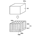
- a plurality of bottomed micropores 102b and an alumina (Al 2 O 3 ) layer are formed on the aluminum material 101 by electrolytic oxidation of the anodized aluminum material 101 from the surface 101s side to the middle.
- a flexible substrate 10A including the porous anodized insulating film 102 made of 102a can be formed.
- Electrolytic oxidation is carried out by using an anodized metal body 101 as an anode, carbon or aluminum as a cathode (counter electrode), immersing them in an anodizing electrolyte, and applying a voltage between the anode and the cathode. It can.
- the electrolytic solution is not limited, and an acidic electrolytic solution containing one or more acids such as sulfuric acid, phosphoric acid, chromic acid, oxalic acid, sulfamic acid, benzenesulfonic acid, and amidosulfonic acid is preferably used.
- the pitch between adjacent fine holes 102b can be controlled in the range of 10 to 500 nm, and the diameter of the fine holes can be controlled in the range of 5 to 400 nm.
- Japanese Patent Application Laid-Open Nos. 2001-9800 and 2001-138300 disclose methods for finely controlling the formation position and the hole diameter of fine holes. By using these methods, the fine holes 102b having an arbitrary hole diameter and depth within the above range can be arranged in a substantially regular manner.
- a flexible substrate 10B shown in FIG. 2B is a clad material provided with a carbon steel or a ferritic steel material 103 on the surface of the aluminum material 101 on which the porous anodic oxide insulating film 102 is not formed. Examples thereof include steel materials made of carbon steel and ferritic stainless steel described in JP2009-132996A.
- the flexible substrate 10B having such a configuration is a flexible and high-strength metal substrate with an insulating layer.
- the thickness of the steel material 103 is not particularly limited, but if it is too thick, the flexibility of the substrate is inhibited, and if it is too thin, the strength of the substrate is inhibited.
- the thickness is preferably 5 to 200 ⁇ m, more preferably 20 to 100 ⁇ m.
- the thickness of the aluminum material 101 is 2 ⁇ m or more in order to prevent the porous anodized insulating film 102 from directly contacting the steel material 103 and to ensure the above-described heat conduction in the substrate surface.
- the thickness refers to the interval between the center lines of the interface irregularities in the structure cross section.
- a symmetrical structure including the aluminum material 101 and the porous anodic oxide insulating film 102 formed on the surface thereof may be provided on both sides of the steel material 103 as in the flexible substrate 10C.
- the laminates 1A to 1C are used in a batch-type manufacturing process of the structure 2 including elements having specific functions, it is necessary to have durability in the manufacturing process of the structure 2.
- the element having a specific function is not particularly limited, but a device having a thin film transistor (TFT), such as a solar cell, an organic EL display, an X-ray flat panel detector (FPD), which is also listed in the “Background Art” section. ) And the like.
- TFT thin film transistor
- FPD X-ray flat panel detector
- the heat resistance of the substrate or the like required during production is preferably 350 ° C. or higher, more preferably 400 ° C. or higher, and further preferably 450 ° C. or higher.
- the adhesive 11 has heat resistance required in the manufacturing process of the structure 2, and the adhesive force is reduced by the irradiation of the laser light L, so that the flexible substrate 10 and the light transmissive support 12 are bonded. Although it will not be restrict
- Having heat resistance required in the manufacturing process means that the state in which the object is adhered can be maintained at the maximum process temperature during the manufacturing process, and the adhesive is not decomposed and no degassing component is generated.
- Suitable examples of the adhesive include an epoxy resin, an acrylic resin, a polyolefin resin, a polyurethane resin, and a silicone resin.
- a silicone resin is preferable.
- silicone resins they are classified into condensation reaction type silicone, addition reaction type silicone, ultraviolet ray curable type silicone and electron beam curable type silicone depending on the curing mechanism, and any of them can be used. Of these, addition-reactive silicone is preferred because of its easy curing reaction and high heat resistance.
- Silicone resins are classified into a solvent type, an emulsion type, and a solventless type, and any type can be used. Among these, a solventless type is preferable. This is because productivity, safety, and environmental characteristics are excellent. Further, since a solvent that causes foaming is not included at the time of curing when forming the resin layer, that is, at the time of heat curing, ultraviolet curing, or electron beam curing, bubbles are unlikely to remain in the resin layer.
- KNS-320A, KS-847, and TPR6700 are silicones that contain a main agent and a crosslinking agent in advance.
- organopolysiloxane adhesives which have heat resistance in a production process exceeding 450 ° C. described in JP 2012-86527 A and can be easily peeled off in a short time. .
- the method for adding the adhesive 11 is not particularly limited, but a coating method such as spin coating or bar coating is simple and preferable. What is necessary is just to design the application quantity of the adhesive material 11 suitably according to the physical property of the adhesive material 11 so that a peeling characteristic may become favorable.
- the adhesive 11 may be added to the pasting area on the surface of the light-transmitting support 12 where the flexible substrate 10 is pasted, but the flexible substrate 10 has a structure 2 including a specific functional element. It is added so as to be firmly fixed to the light transmissive support 12 in the manufacturing process.
- the affixing region is not shown and is shown as an aspect in which the adhesive 11 is uniformly applied to the entire surface of the light transmissive support 12, but in the manufacturing process of the structure 2. As long as it is firmly fixed, the size of the pasting amount area and the adhesive material adding area may be different.
- the light-transmitting support is a support having a transmittance of 10% or more with respect to laser light.
- the transmittance is preferably 60% or more, more preferably 80% or more.
- the light-transmitting support 12 is not particularly limited as long as it has heat resistance in the manufacturing process of the structure 2. However, the light-transmitting support 12 and the light-transmitting support 12 If the difference in linear expansion coefficient with the flexible substrate 10 is large, wrinkles may occur in the entire substrate or cracks may occur in the porous anodized insulating film 102.
- the linear expansion coefficients of the flexible substrate 10 and the light-transmissive support 12 are as close as possible, and the difference between these linear expansion coefficients (CTE: Coefficient of Temperature Expansion) is within 4 ppm / K. Is preferable, and it is more preferably within 2 ppm / K.
- the linear expansion coefficient of the flexible substrate 10 is determined by placing the sample (flexible substrate 10) on a temperature-variable hot plate and measuring the distance between the scores on the sample surface at each temperature without any weight.
- the rate of change in distance between ratings from room temperature to 500 ° C. is defined as the coefficient of linear expansion (CTE).
- FIG. 4 shows a flexible substrate 10C (Type A in the figure) having an anodized insulating film 102 on both surfaces of an aluminum material 101, and an anodized insulating film on a clad material of a ferritic stainless steel material 103 and an aluminum material 101.
- 10 is a diagram showing thermal expansion characteristics of a flexible substrate 10B (Type B in the figure) provided with 102 measured by the above method.
- the slope of the graph in FIG. 4 corresponds to the coefficient of linear expansion (CTE).
- the CTEs of the flexible substrate 10C and the flexible substrate 10B were about 5 ppm / K and 10 ppm / K, respectively.
- This numerical value is a result of the material combination of the porous anodized insulating film 102 and the aluminum material 101, and the porous anodized insulating film 102, the aluminum material 101, and the ferritic steel material 103.
- the present inventors have confirmed that there is almost no change within the range of This is because in the embodiment of the flexible substrate 10A provided with the porous anodic oxide insulating film 102 only on one side and also in the flexible substrate 10B, a symmetric structure, that is, the porous anodic oxide insulating film 102, the aluminum material 101, and ferrite. It has been confirmed that the CTE is about 5 and 10 ppm / K, respectively, in the metal substrate with an insulating layer made of the steel material 103, the aluminum material 101, and the porous anodized insulating film 102.
- the light transmissive support 12 includes CTE. Is preferably 3 to 9 ppm / K.
- borosilicate glass and alkali-free glass are preferably exemplified as the substrate having excellent transparency.
- the flexible substrate 10B that is, the flexible substrate 10 including the porous anodized insulating film 102 on the clad material of the ferritic stainless steel material 103 and the aluminum material 101, and the flexible substrate 10B.
- CTE is preferably 6 to 13 ppm / K, and among such supports, examples of the substrate having excellent transparency include white plate potash glass and soda lime glass.
- the thickness of the light-transmitting support 12 can be selected from any thickness that can be used in the manufacturing apparatus. However, if it is too thin, handling becomes difficult and the function of the support is not achieved. There is a risk of warping the whole. A typical thickness is 0.3 to 1.2 mm.
- the electronic device manufacturing method of the present invention has a specific function on the flexible substrate 10 (10A, 10B, 10C) provided with the porous anodized insulating film 102 on the aluminum material 101.
- an electronic device 3 formed with an element (structure 2) is formed by combining a flexible substrate 10 having a porous anodized insulating film 102 on an aluminum material 101 and a light transmissive support 12. Then, an element (structure 2) is formed on the porous anodic oxide insulating film 102 after the laminated body 1 (1A, 1B, 1C) attached through the heat-resistant adhesive 11 in FIG.
- a high-performance flexible electronic device can be manufactured on a flexible metal substrate by a batch method.
- the electronic device manufacturing method and laminate according to the present invention are suitable for manufacturing photoelectric conversion elements (thin film compound solar cells) (electronic devices 3), organic EL displays, X-ray detectors, and organic thin film solar cells described below. Can be used for manufacturing photoelectric conversion elements (thin film compound solar cells) (electronic devices 3), organic EL displays, X-ray detectors, and organic thin film solar cells described below. Can be used for manufacturing photoelectric conversion elements (thin film compound solar cells) (electronic devices 3), organic EL displays, X-ray detectors, and organic thin film solar cells described below. Can be used for manufacturing photoelectric conversion elements (thin film compound solar cells) (electronic devices 3), organic EL displays, X-ray detectors, and organic thin film solar cells described below. Can be used for manufacturing photoelectric conversion elements (thin film compound solar cells) (electronic devices 3), organic EL displays, X-ray detectors, and organic thin film solar cells described below. Can be used for manufacturing photoelectric conversion elements (thin film
- any electronic device first, a laminate 1 in which a flexible substrate 10 and a light transmissive substrate 12 are bonded together with an adhesive 11 is prepared, and the laminate 1 on the flexible substrate 10 ( An electronic device is formed on the porous anodized insulating film 102).
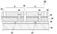
- FIG. 5 is a schematic cross-sectional view of a thin film compound photoelectric conversion element 3A manufactured by the method for manufacturing an electronic device of the present invention and a laminate.
- the photoelectric conversion element 3A is an element having a basic structure of a laminated structure in which a lower electrode (back electrode) 20, a photoelectric conversion semiconductor layer 30, a buffer layer 40, and an upper electrode 50 are sequentially laminated on a flexible substrate 10. is there.
- the photoelectric conversion element 3A includes a first groove portion 61 that penetrates only the lower electrode 20, a second groove portion 62 that penetrates the photoelectric conversion layer 30 and the buffer layer 40, and the photoelectric conversion layer 30 and the buffer.
- a third groove 63 that penetrates the layer 40 and the upper electrode 50 is formed.
- (Earth) A metal supply layer, a diffusion preventing layer for suppressing diffusion of the alkali metal and the like from the metal supply layer to the flexible substrate 10 side, and the like may be provided.
- a laminate 1 in which a flexible substrate 10 and a light transmissive substrate 12 are bonded together with an adhesive 11 is prepared, and the flexible substrate 10 of the laminate 1 (porous anodic oxide insulating film 102) is prepared.
- the upper electrode layer 20 made of a transition metal such as Mo having a thickness of 450 nm is formed by sputtering or the like.
- a part of the conductive layer 20 is removed by laser scribing to form the separation groove 61, and the compound semiconductor photoelectric conversion layer 30 is formed thereon by a vapor deposition method or the like.
- the photoelectric conversion layer 30 is preferably made of a II-VI group semiconductor such as CdTe or an I-III-VI group semiconductor represented by CuInGaSe 2 .
- the group I-III-VI semiconductor CuAlS 2, CuGaS 2, CuInS 2, CuAlSe 2, CuGaSe 2, AgAlS 2, AgGaS 2, AgInS 2, AgAlSe 2, AgGaSe 2, AgInSe 2, AgAlTe 2, AgInTe 2 , Cu (In, Al) Se 2 , Cu (In, Ga) (S, Se) 2 , Cu 1 -z In 1 -x Ga x Se 2 -y S y (where 0 ⁇ x ⁇ 1, 0 ⁇ y ⁇ 2, 0 ⁇ z ⁇ 1) (CI (G) S), Ag (In, Ga) Se 2 , Ag (In, Ga) (S, Se) 2 and the like.
- a multi-source simultaneous vapor deposition method is particularly suitable.
- a typical method is a three-step method (JRTuttle et.al, Mat. Res. Soc. Symp. Proc., Vol. 426 (1996) p. 143, etc.).
- In, Ga, and Se are co-deposited in a high vacuum at a substrate temperature of 400 ° C., then heated to 500 to 560 ° C., and Cu and Se are co-deposited, and then In, Ga, and Se are further co-deposited. To do.
- the substrate temperature in the second and third stages in the three-stage method is 550 ° C.
- K (In 0.7 Ga 0.3 ) Se 2 is 2 ⁇ m using a K cell (knudsen-Cell) as an evaporation source. Form a film.
- the buffer layer 40 is formed on the photoelectric conversion layer 30.
- the buffer layer 40 for example, CdS is formed with a thickness of, for example, 50 nm by a CBD method (chemical bath deposition method) or the like, and the layers from the predetermined position on the surface of the buffer layer 40 to the photoelectric conversion layer 30 are removed to form a separation groove. 62 is formed by mechanical scribing or the like.
- the transparent electrode 50 for example, an Al—ZnO layer is formed with a thickness of 300 nm by sputtering from the upper surfaces of the separation grooves 62 and the buffer layer 40, and further, the separation grooves 63 for dividing the cells are patterned by mechanical scribing or the like.
- the photoelectric conversion element structure 2 formed on the flexible substrate 10 of the laminate 1 is obtained.
- the laser beam L is irradiated from the back side of the laminate 1 to reduce the adhesive strength of the adhesive 11, and the light transmissive substrate 12 is peeled from the laminate 1, and photoelectric conversion is performed on the flexible substrate 10.
- a photoelectric conversion element 3A in which the element structure 2 is formed is obtained.
- FIG. 6 is a cross-sectional view schematically showing the main components of the organic EL display 3B manufactured by the method for manufacturing an electronic device of the present invention and the laminate.
- the organic EL display 3 ⁇ / b> B has a configuration in which a TFT 80 and an organic EL element 98 are stacked on the TFT 80 as the structure 2 including an element having a specific function on the flexible substrate 10. is doing.
- a laminate 1 in which a flexible substrate 10 and a light transmissive base material 12 are bonded together with an adhesive 11 is prepared, and a TFT 80 and a TFT 80 are provided on the laminate 1.
- An organic EL element 98 is formed thereon.
- a buffer layer (Si 3 N 4 ) 71 is formed on the porous anodic oxide insulating film 102 of the multilayer body 1 by plasma CVD, and further a thickness of 200 nm is formed on the buffer layer (Si 3 N 4 ) 71. Then, a SiO 2 layer (insulating film) 72 is formed on the entire surface by plasma CVD. The film formation temperature was 350 ° C. for both.
- a thin film transistor 80 (hereinafter referred to as TFT 80) is formed for each pixel.
- the capacitor 90 is formed at the same time.
- the gate electrode 81 of the TFT 80 and the lower electrode 91 of the capacitor 90 are formed by patterning by a photolithography method and an etching method.
- the material of the gate electrode 81 and the lower electrode 91 is not limited to Mo, and other known conductive materials can be used.
- metals such as Al, Cr, Ta, Ti, Au, Ag, alloys such as Al—Nd, APC, tin oxide, zinc oxide, indium oxide, indium tin oxide (ITO), indium zinc oxide (IZO), etc.
- metal conductive films organic conductive compounds such as polyaniline, polythiophene, and polypyrrole, or mixtures thereof.
- the film forming method and the patterning method may be appropriately selected depending on the material to be used, etc.
- the film forming method in addition to the sputtering method, for example, a physical method such as a vacuum evaporation method, an ion plating method, Examples include chemical methods such as CVD and plasma CVD, and wet methods such as a printing method and a coating method.
- patterning may be performed by a lift-off method, or a metal mask (shadow mask) having an opening corresponding to a pattern of a gate electrode to be formed may be used.
- a metal mask shadow mask
- an SiO 2 layer (thickness: 200 nm) is formed as the insulating layer 82.
- the insulating layer 82 functions as a gate insulating layer in the TFT 80, and functions as a dielectric filling the space between the electrodes in the capacitor 90.
- the SiO 2 film was formed by plasma CVD at a film forming temperature of 350 ° C.
- an InGaZnO 4 layer (thickness: 50 nm) is formed.
- the active layer is formed by sputtering or the like, and is patterned according to the shape.
- the gate insulating layer 82 may have a single layer structure made of an insulator such as SiN x , SiON, Al 2 O 3 , Y 2 O 3 , Ta 2 O 5 , HfO 2, or the insulation thereof.
- an insulator such as SiN x , SiON, Al 2 O 3 , Y 2 O 3 , Ta 2 O 5 , HfO 2, or the insulation thereof.
- a laminated structure in which two or more body compounds are laminated may be used.
- a polymer insulator such as polyimide may be used.
- the active layer 83 is preferably an amorphous oxide semiconductor from the viewpoint of mobility and property uniformity.
- the active layer 83 is an oxide containing at least one of In, Ga, and Zn, for example, an oxide containing In, In And an oxide containing Zn, and an oxide containing In, Ga and Zn, and the composition structure is preferably InGaO 3 (ZnO) m (m is a natural number of less than 6).
- ZnO Zinc
- m is a natural number of less than 6
- a p-type oxide semiconductor such as ZnO.Rh 2 O 3 , CuGaO 2 , or SrCu 2 O 2 may be used for the active layer, or an oxide semiconductor disclosed in JP-A-2006-165529 may be used. It may be used.
- amorphous silicon and polycrystalline silicon used for TFTs in liquid crystal displays can also be used.
- Amorphous silicon is deposited by plasma CVD at a deposition temperature of 350 ° C.
- Polycrystalline silicon can be obtained by laser annealing amorphous silicon using an excimer laser.
- the active layer is patterned by photolithography and etching, and AlNd (thickness: 100 nm) to be the source / drain electrodes 84 and 85 and the upper electrode 93 of the capacitor 90 is formed by sputtering to form the source / drain.
- the drain electrodes 84 and 85 and the upper electrode 93 are patterned.
- the formation of the source / drain electrodes 84 and 85 and the upper electrode 93 can be appropriately adopted from the materials exemplified in the formation of the gate electrode 81, the film forming method, the patterning method, and the like.
- the bottom contact type TFT 80 having the active layer 83 formed before the source / drain electrodes 84 and 85 is formed.
- the structure of the TFT 80 is not limited to the above, and may be selected as appropriate.
- a bottom contact type TFT in which an active layer is formed after a source / drain electrode may be used, or a top gate type TFT in which a source / drain electrode is formed before a gate electrode may be used.
- an interlayer insulating planarizing layer 88 is formed on the TFT 80 and the capacitor 90 to planarize the laminated surface.
- a resin layer thickness: 1.5 ⁇ m
- the interlayer insulating planarizing layer may have a two-layer structure such as an inorganic insulating layer / planarizing resin layer from the flexible substrate side.
- an inorganic insulating film such as SiO 2 , Si 3 N 4 , or SiON can be used, and the above-mentioned acrylic resin or the like can be used for the planarizing resin layer.
- a through hole (not shown) that exposes a part of the source electrode 84 and a through hole 94 that exposes a part of the upper electrode 93 are formed in the resin layer 88, and then the source electrode 84 is formed through the through hole 94.
- a pixel electrode 95 which is connected to a part and serves as an anode or a cathode is formed.
- the pixel electrode 95 is formed, for example, by forming a conductive film such as Al, Mo, IZO, or ITO by sputtering and then patterning by photolithography and etching. Further, the pixel electrode may be formed using a metal mask corresponding to the pattern of the pixel electrode to be formed.
- the organic EL layer 96 is a layer including at least a light emitting layer, and a hole injection layer, a hole transport layer, an electron injection layer, an electron transport layer, a block layer, and the like are formed as necessary.
- the configuration of the organic EL element 98 including the anode and the cathode for example, the following layer configuration can be adopted, but is not limited to these layer configurations, and may be appropriately determined according to the purpose and the like.
- a transparent electrode 97 is formed by depositing ITO over the entire surface as an electrode on the light extraction side.
- the electrode 97 on the light extraction side does not need to be divided for each pixel, and may be formed on the entire surface of the organic EL layer 96 by a sputtering method to be a common electrode.
- a barrier layer that blocks moisture and oxygen is formed to prevent the organic EL element from being deteriorated by moisture and oxygen.
- the barrier layer silicon nitride, silicon oxide, silicon oxynitride, oxide
- An inorganic substance such as aluminum can be used.
- Resin materials constituting the resin film 99 include polyesters such as polyethylene terephthalate, polybutylene phthalate, and polyethylene naphthalate, polystyrene, polycarbonate, polyethersulfone, polyarylate, polyimide, polycycloolefin, norbornene resin, and poly (chlorotrifluoro). And organic materials such as ethylene).
- the laser beam L is irradiated from the back side of the laminate 1 to reduce the adhesive strength of the adhesive 11, and the light transmissive substrate 12 is peeled from the laminate 1, and the light emitting element is formed on the flexible substrate 10.
- An organic EL display 3B in which the structure 2 is formed can be manufactured.
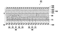
- FIG. 7 is a cross-sectional view schematically showing the main components of the FPD 3C manufactured by the manufacturing method and the laminate 1 of the present embodiment.
- the FPD 3C includes a TFT 80 having a-Si as a channel layer as a structure 2 including an element having a specific function on a flexible substrate 10, and a photodetector 100 made of an organic material on the TFT 80. And the scintillator 105 are stacked. Also in the manufacture of the FPD 3C, first, a laminated body 1 in which a flexible substrate 10 and a light transmissive substrate 12 are bonded together with an adhesive 11 is prepared, and a TFT 80 and a photo detector on the TFT 80 are prepared. 100 and a scintillator 105 are formed.
- a SiN film 73 is formed on the porous anodic oxidation insulating film 102 of the laminate 1 by plasma CVD, and then a Ge Ti / Al / Ti film is formed. Through a normal photolithography process, the gate electrode 81 and the capacitor 90 are formed. The lower electrode 91 is formed.
- a SiO 2 insulating film, an amorphous Si layer, and a SiN protective film are successively formed by plasma CVD.
- the film forming temperature is 350 ° C.
- An amorphous Si active layer (channel) 83 is formed by patterning the amorphous Si layer and the Si protective film in a normal photolithography process.
- the SiO 2 insulating film functions as a gate insulating layer 82 in the TFT 80, and functions as a dielectric that fills between the electrodes in the capacitor 90.
- a Mo film to be the source / drain electrodes 84 and 85 and the upper electrode 93 of the capacitor 90 is formed and patterned into the source / drain electrodes 84 and 85 and the upper electrode 93.
- the TFT 80 and the capacitor 90 are formed.
- a planarizing film 88 is applied and formed on the TFT 80 and the capacitor 90, and a through via for connection to the capacitor 90 is formed in the planarizing film 88, and then the lower electrode 101 for the photodetector is formed.
- An organic photoelectric conversion unit 102 made of a photosensitive organic material and an upper electrode 103 for the photodetector are formed thereon to form the photodetector 100.
- the sheet scintillator 105 is pasted on the photodetector 100.
- a material of the scintillator 105 CaWO 4 , Gd 2 O 2 S, CsI, or the like can be appropriately applied.
- a sealing film 108 is further attached on the scintillator 105.
- a protective film 109 (PET film) to be prevented can be attached to manufacture the X-ray FPD 3C in which the photoelectric conversion element structure 2 is formed on the flexible substrate 10.
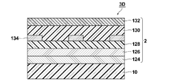
- FIG. 8 is sectional drawing which shows typically the structure principal part of organic thin-film solar cell 3D manufactured with the manufacturing method and laminated body of the said electronic device of this invention.
- the organic thin-film solar cell 3 ⁇ / b> D basically has a stacked structure in which a lower electrode 124, an organic photoelectric conversion semiconductor layer 126, a buffer layer 40, and an upper electrode 128 are sequentially stacked on a flexible substrate 10. It is an element to be configured. Also in the manufacture of the organic thin film solar cell 3D, first, the laminate 1 in which the flexible substrate 10 and the light transmissive base material 12 are bonded together with the adhesive 11 is prepared, and then 3.92 mass of pure water.
- the coating liquid mixed at a ratio of 15 parts by weight, 0.05 parts by weight of 35% hydrochloric acid, 12.53 parts by weight of ethanol, and 4.17 parts by weight of tetraethoxysilane was applied to the surface of the anodic oxide film of the flexible substrate 10. , Dried. Application was performed by dip coating. Then, the laminated body 1 which apply
- Titanium (thickness 5 nm) and silver (thickness 100 nm) were continuously vacuum-deposited on the protective layer surface of the laminate 1 produced in this manner to form the lower electrode 124. At this time, a shadow mask was used so that the element area was 16 cm 2 .
- the lower electrode 124 when functioning as a negative electrode, for example, metals such as magnesium, aluminum, calcium, titanium, chromium, manganese, iron, copper, zinc, strontium, silver, indium, tin, barium, bismuth, etc. And alloys thereof are preferably used.
- the lower electrode 124 functions as a positive electrode
- a metal such as chromium, cobalt, nickel, copper, molybdenum, palladium, silver, tantalum, tungsten, platinum, gold, or an alloy thereof
- TCO transparent conductive oxide
- Conductive polymers such as polyaniline, polythiophene, and polypyrrole are preferably used.
- the conductive polymer layer suitable for the lower electrode 124 is disclosed in detail in Japanese Patent Application Laid-Open No. 2012-43835, and a polythiophene derivative is preferable, and polyethylenedioxythiophene-polystyrenesulfonic acid (PEDOT-PSS) is more preferable.
- PEDOT-PSS polyethylenedioxythiophene-polystyrenesulfonic acid
- a PEDOT-PSS aqueous solution (manufactured by Heraeus Precious Metals, Clevios P VP.AI 4083) was spin-coated on the lower electrode 124 and heat-treated at 140 ° C. for 15 minutes. This formed a positive hole transport layer (film thickness 0.04 micrometer).
- a composition in which P3HT (manufactured by Merck, lisicon SP001) as an electron donating material and ICBA (manufactured by Sigma-Aldrich) as an electron accepting material are dissolved in dichlorobenzene at a weight ratio of 1: 1 on the hole transport layer, It spin-coated on the positive hole transport layer in dry nitrogen atmosphere, and heat-processed for 15 minutes at 140 degreeC.
- a bulk heterojunction photoelectric conversion layer 126 was formed.
- the film thickness of the photoelectric conversion layer 126 was 0.2 ⁇ m.
- the photoelectric conversion layer 126 After the photoelectric conversion layer 126 receives visible light such as sunlight and generates excitons (electron-hole pairs), the excitons dissociate into electrons and holes, and the electrons move to the negative electrode side.
- the material is selected from materials that exhibit a highly efficient photoelectric conversion process of being transported to the positive electrode side.
- a photoelectric conversion layer including an electron donating region (donor) made of an organic material is formed, and from the viewpoint of conversion efficiency, a bulk heterojunction photoelectric conversion layer 126 (hereinafter referred to as “to bulk”).
- the “terror layer” is also preferably applied.
- the bulk hetero layer is an organic photoelectric conversion layer in which an electron donating material (donor) and an electron accepting material (acceptor) are mixed.
- the mixing ratio of the electron-donating material and the electron-accepting material is adjusted so that the conversion efficiency is the highest, but is usually selected from the range of 10:90 to 90:10 by mass ratio.
- a co-evaporation method is used as a method for forming such a mixed layer.
- the film thickness of the bulk hetero layer is preferably 10 to 500 nm, particularly preferably 20 to 300 nm.
- the electron donating material (also referred to as a donor or hole transporting material) is a ⁇ electron conjugated compound having a highest occupied orbital (HOMO) level of 4.5 to 6.0 eV.
- conjugated polymers or phenylene vinylene polymers obtained by coupling various arenes (for example, thiophene, carbazole, fluorene, silafluorene, thienopyrazine, thienobenzothiophene, dithienosilole, quinoxaline, benzothiadiazole, thienothiophene).
- various arenes for example, thiophene, carbazole, fluorene, silafluorene, thienopyrazine, thienobenzothiophene, dithienosilole, quinoxaline, benzothiadiazole, thienothiophene.
- porphyrins and phthalocyanines for example, thiophene, carbazole, fluorene, silafluorene, thienopyrazine, thienobenzothiophene, dithienosilole, quinoxaline, benzothiadiazole,
- a conjugated polymer obtained by coupling a structural unit selected from the group consisting of thiophene, carbazole, fluorene, silafluorene, thienopyrazine, thienobenzothiophene, dithienosilole, quinoxaline, benzothiadiazole, and thienothiophene is particularly preferable.
- Specific examples include poly-3-hexylthiophene (P3HT), poly-3-octylthiophene (P3OT), various polythiophene derivatives described in Journal of the American Chemical Society Vol. 130, p.
- An electron-accepting material (also referred to as an acceptor or an electron-transporting material) is a ⁇ -electron conjugated compound whose lowest unoccupied orbital (LUMO) level is 3.5 to 4.5 eV.
- fullerene and derivatives thereof include fullerene and derivatives thereof, phenylene vinylene polymers, naphthalene tetracarboxylic imide derivatives, and perylene tetracarboxylic imide derivatives. Of these, fullerene derivatives are preferred. Specific examples of fullerene derivatives include C 60 , phenyl-C 61 -butyric acid methyl ester (fullerene derivatives referred to as PCBM, [60] PCBM, or PC61BM in the literature), C 70 , phenyl-C 71 -butyric acid methyl ester.
- PCBM Compactene derivatives referred to as PCBM, [70] PCBM, or PC71BM in many literatures
- fullerene derivatives described in Advanced Functional Materials Vol. 19, pages 779-788 (2009) Journal of the American Chemical Examples include fullerene derivatives SIMEF described in Society Vol. 131, page 16048 (2009), fullerene derivatives ICBA described in Journal of the American Chemical Society vol. 132, page 1377 (2010), and the like.
- Aluminum (film thickness 2 nm) and silver (film thickness 10 nm) were continuously vacuum-deposited on the photoelectric conversion layer 126. At this time, a shadow mask was used so that the element area was 16 cm 2 . Subsequently, silver (film thickness 0.4 ⁇ m) was vacuum deposited on the upper electrode 128 as the bus electrode 34. At this time, a striped bus electrode 134 having a line width of 0.3 mm and a pitch of 20 mm was formed using a shadow mask having a stripe pattern. Furthermore, ITO (film thickness 0.1 ⁇ m) is formed through a shadow mask with an opening of 16 cm 2 by high-frequency magnetron sputtering while heating the substrate to 160 ° C. in an atmosphere of 1 Pa with Ar gas and O 2 gas introduced. Then, an optically transparent upper electrode 128 having a three-layer laminated structure of aluminum / silver / ITO having a bus electrode 134 between the aluminum layer and the ITO layer was formed.
- the upper electrode 128 is preferably formed of a transparent conductive film in order to allow light to enter the photoelectric conversion layer.
- the transparent conductive film include metals, metal oxides, conductive polymers, mixtures thereof, and laminated structures. Specific examples include TCO such as tin oxide, zinc oxide, indium oxide, indium tin oxide (ITO), indium zinc oxide (IZO), indium tungsten oxide (IWO), metals and metals mentioned as the lower electrode 124 described above. Examples include ultrathin alloy films, conductive polymers such as polyaniline, polythiophene, and polypyrrole.
- TCO materials are ITO, IZO, tin oxide, antimony-doped tin oxide (ATO), fluorine-doped tin oxide (FTO), zinc oxide, antimony-doped zinc oxide (AZO), and gallium-doped zinc oxide (GZO). Any of the materials.
- the upper electrode 128 may be formed by a known method.
- PVD methods such as wet film formation methods by coating and printing, vacuum deposition methods, sputtering methods, ion plating methods, and dry film formation methods by CVD methods. What is necessary is just to form by the method selected suitably.
- an organic EL element manufacturing apparatus in which a vacuum deposition apparatus for forming aluminum and silver and a sputtering apparatus for forming ITO are directly connected to a cluster type vacuum transfer system having a degree of vacuum of 1 ⁇ 10 ⁇ 4 Pa or less. was done using.
- a PEN film in which a silicon nitride film and an acrylate polymer were laminated was prepared as the gas barrier film 132.
- This gas barrier film 132 was laminated by vacuum heating at 140 ° C. with an ethylene-vinyl acetate copolymer (EVA) film as a sealant interposed therebetween, and the gas barrier film 132 was laminated.
- EVA ethylene-vinyl acetate copolymer
- the laser beam L is irradiated from the back side of the laminate 1 to reduce the adhesive strength of the adhesive 11, and the light-transmitting base material 12 is peeled off from the laminate 1.
- An organic thin film solar cell 3D in which the conversion element structure 2 is formed can be manufactured.
- the electronic device to be manufactured may be selected according to the purpose.
- the present invention can be suitably applied to the manufacture of electronic paper and a liquid crystal display.
- the electrodes (wirings) formed on the resin films on both sides are arranged to face each other so that they intersect vertically and horizontally, and between these electrodes, the coloring materials and display materials used in organic EL elements and electronic paper
- the electronic device may be provided, or a passive device such as a color filter may be used.
- Example 1 to 15 and Comparative Example 1 Using the laminates of Examples 1 to 15 and Comparative Example 1 shown in Table 1, the electronic device manufacturing method and laminate of the present invention were evaluated.
- As the adhesive a cured silicone resin layer produced by the following method was used.
- component (A) linear vinylmethylpolysiloxane (“VDT-127”, viscosity at 25 ° C., 700-800 cP (centipoise): manufactured by Azumax, mol% of vinyl group in 1 mol of organopolysiloxane),
- component (B) linear methylhydropolysiloxane (“HMS-301”, viscosity 25-35 cP (centipoise) at 25 ° C .: manufactured by Azmax: 8 hydrogen atoms bonded to silicon atoms in one molecule)
- a molar ratio of all alkenyl groups to hydrogen atoms bonded to all silicon atoms (hydrogen atom / alkenyl group) is 0.9, and 100 parts by weight of this siloxane mixture, component (D)
- component (D) As a result, 0.3 part by mass of 1-ethynyl-1-cyclohexanol was added.
- a platinum-based catalyst (CAT-PL-56, manufactured by Shin-Etsu Silicone Co., Ltd.) is added so that the total amount of the component (A) and the component (B) is 1500 ppm in terms of platinum. A composition was obtained.
- the obtained composition was coated on the surface of the light-transmitting support by a spin coater (2000 rpm, 20 seconds, coating amount 20 g / m 2 ). Thereafter, the mixture coated on the transparent support was heat-cured at 180 ° C. for 60 minutes in the air to form an adhesive composed of a cured silicone resin layer having a thickness of 30 ⁇ m on the light-transmissive support.
- the surface tension of the cured silicone resin layer was 20.2 N / m.
- a SiO 2 film was sequentially formed on the surface of the anodized insulating film with a thickness of 1000 nm / Mo film 100 nm / Sn film 100 nm, and then from the back side of the light transmissive support, YAG The laser was irradiated and peeled off by two-dimensional scanning.
- the SiO 2 film was formed by spin coating (AZ Spinfi 1600) and then baked in an oven at 400 ° C. for 60 minutes.
- the Mo film and Sn film were formed by sputtering at room temperature.
- the YAG laser was irradiated by scanning successively with a beam width of 200 ⁇ m ⁇ 2.5 ⁇ m, an energy density of 100 kW / cm 2 and a scanning speed of 200 mm / s.
- the linear expansion coefficients of the flexible substrate and the light transmissive support were determined by the method described above.
- the evaluation was performed according to the state of the Sn film on the flexible substrate after peeling. Sn film has good melting and no cracks, wrinkles, etc. Sn film has some cracks and wrinkles, but melting is not seen, no problem is allowed, Sn film is melting Things were made impossible. The melting of the Sn film is considered to have risen to 231.9 ° C. or higher, which is the melting point of the film surface.
- Example 16 Using the laminate of Example 3, the organic EL display of the above embodiment was produced.
- the conditions of the laser peeling process were the same as in Example 3. Before and after the laser peeling process, no change was seen in the light emission efficiency of the organic EL element, and the acrylic resin of the interlayer insulating planarizing layer was also discolored. Thus, a flexible organic EL display having good characteristics could be produced.
Landscapes
- Engineering & Computer Science (AREA)
- Manufacturing & Machinery (AREA)
- Electroluminescent Light Sources (AREA)
- Laminated Bodies (AREA)
- Devices For Indicating Variable Information By Combining Individual Elements (AREA)
Abstract
【課題】バッチ式プロセスにより可撓性基板上に高性能な電子デバイスを製造する。 【解決手段】アルミニウム材(101)上に多孔質陽極酸化絶縁膜(102)を備えた可撓性基板(10)の多孔質陽極酸化絶縁膜(102)上に、特定の機能を有する素子を含む構造体(2)が形成されてなる電子デバイス(3)の製造方法であって、可撓性基板(10)と光透過性支持体(12)とを用意し、光透過性支持体(12)の表面の可撓性基板(10)が貼付される貼付領域に構造体(2)の形成工程中において耐熱性を有する接着剤(11)を付加し、可撓性基板(10)を光透過性支持体(12)に接着剤(11)を介して貼り付け、多孔質陽極酸化絶縁膜(102)上に構造体(2)を形成し、光透過性支持体(12)の裏面側からレーザー光(L)を照射することにより、接着剤(11)の接着力を低下させて光透過性支持体(12)を可撓性基板(10)から剥離する。
Description
本発明は、薄型トランジスタを備えた液晶・有機ELディスプレイ、電子ペーパーやX線センサ等、太陽電池等の電子デバイス、特に可撓性を有する電子デバイスの製造方法および該製造方法に用いられる積層体に関するものである。
薄膜トランジスタ(TFT)を備えた液晶ディスプレイ、有機ELディスプレイなどの電子デバイスにおいては、TFTを形成する基板として、一般的にガラス基板が用いられており、電子デバイスのフレキシブル化、軽量化、薄型化への要求に応じて、そのガラス基板の厚さの薄型化が進められている。また一方、更なるフレキシブル化、軽量化、薄膜化を実現するために、TFTを形成する基板としてプラスチック基板などの樹脂フィルムや薄型金属基板を用いることも検討されている。
特に金属基板は、樹脂フィルムに比して耐熱性が高いこと、また薄型ガラス基板に比して脆く(割れ)ないことから、高温プロセスが必要となるデバイスに適用可能な可撓性基板として有用である。
可撓性基板上にTFT等の特定の機能を有する素子を含む構造体(以下、機能素子構造体)を備えた電子デバイスの作製方法としては、可撓性基板上に直接、機能素子構造体を形成する方法(直接法)と、ガラス基板の様なリジッド基板上に機能素子構造体を形成し、機能素子構造体を基板から剥離して可撓性基板上に転写する方法(間接法あるいは転写法)とがある。
間接法あるいは転写法は、機能素子構造体を基板から剥離そして可撓性基板上に転写する、という追加の工程が必要であり、その工程の歩留まりが悪い為に製造には不向きであり、歩留まりの観点から直接法で製造することが好ましい。
直接法において、可撓性基板は、ロール状に巻いた長尺基板を連続的に巻出し、少なくとも1つの工程を経た後に巻取るというロールツーロール方式が可能であり、大量生産にも適している。しかしながら、この方式では新規の製造設備となり、電子デバイスにより様々なロールツーロール製造装置が必要となる。一方で、従来のガラスやシリコンウェハーの様なリジッド基板を用いる際には、確立したバッチ式の製造装置が市販されており、これを流用することにより、低コストで速やかに電子デバイスの製造が可能である。
可撓性基板をバッチ式の製造装置で使用するには、その膜薄性や可撓性のために、ハンドリング性が悪く、工程中に反りを発生したり、可撓性基板上に製膜した材料の影響で歪を生じたりするという問題がある。
かかる問題を解決する方法として、バッチ式の製造装置では、可撓性基板を、シリコンもしくはガラス等の剛性のある支持体(以下、支持体)に固定された状態で使用し、工程通過後に可撓性基板から支持体を剥離する方法が提案されている(特許文献1等)。
支持体に可撓性基板を固定してバッチ式の従来の製造プロセスに用いる場合、製造プロセス中に、可撓性基板と支持体との間に少しでも剥離部分が生じると、その箇所に歪みや反りを生じる恐れがある。従って、製造プロセスにおいて、可撓性基板に反りや歪みを生じさせないために、プロセス途中に部分的な剥離も生じないように、可撓性基板は支持体にしっかりと固定されている必要がある。
一方、機能素子の製造後に支持体を可撓性基板から剥離する際には、できるだけ容易に剥離できることが好ましい。
すなわち、可撓性基板と支持体とは、機能素子作製プロセス中は剥離することはないが、プロセス終了後には容易に剥離させることができるように貼り付けられていることが望まれる。
しかしながら、機能素子作製プロセス中は剥離することがないが、プロセス終了後に容易に剥離させることができるように、両者を接着させるのは非常に困難である。両者の接着力が弱すぎると機能素子作製プロセス中に剥離してしまい、逆に強すぎると支持体を剥離するのが困難となり、強引に剥離させると作製した機能素子や可撓性基板に損傷を生じさせる恐れがある。また、加熱やUV照射することで接着強度が低下する粘着剤で両者を接着させる方法も考えられるが、これらの方法でも、局所的に気泡が発生したり、粘着剤の粘着強度が完全になくなることがない為に上手く可撓性基板から支持体を剥離できないのが現状である。また、機能素子作製プロセスにおいて、例えばプラズマCVDでアモルファスシリコンを製膜する場合には基板温度を350℃程度の高温に上げる必要があり、この際に接着力が低下して支持体から可撓性基板が剥離してしまう、あるいは高温で接着剤の硬化が進行し、工程終了後に可撓性基板から支持体を剥離できなくなるという問題がある。
特許文献1には、樹脂フィルム基板や薄型金属基板を、接着層を用いて固定用支持体に貼りあわせて発光素子を基板上に形成し、発光素子形成後に固定基板側からレーザー光を照射することにより接着層の一部又は全部を気化させて固定用支持体を分離する半導体装置の作製方法が開示されている。
特許文献1では、段落[0018]にも記載されているように、固定用支持体に貼りあわせる際に用いる接着層として、分離に用いるレーザー光で全部又は一部が気化するものであり、また、素子形性工程における加熱により気化しない物性を併せ持つ接着層を採用することにより、基板の厚みが50~300μmの極薄基板を用いて信頼性の高い発光装置をバッチプロセスにより製造可能としている。
しかしながら、特許文献1に記載の方法により、実際にステンレス基板を用いて機能素子の作製を行った場合、レーザー光でガラス固定基板から剥離する際、素子の一部が劣化し、素子の特性均一性の悪化が確認された(後記比較例1を参照)。
本発明は上記事情に鑑みてなされたものであり、可撓性金属基板上に高性能なフレキシブル電子デバイスをバッチ方式で製造する方法、及び、その方法に適した、可撓性基板と支持体との貼りあわせ積層体を提供することを目的とするものである。
本発明の電子デバイスの製造方法は、アルミニウム材上に多孔質陽極酸化絶縁膜を備えた可撓性基板の前記多孔質陽極酸化絶縁膜上に、特定の機能を有する素子を含む構造体が形成されてなる電子デバイスの製造方法であって、
可撓性基板と、光透過性支持体とを用意し、
光透過性支持体の表面の、可撓性基板が貼付される貼付領域に特定の機能を有する素子を含む構造体の形成工程中において耐熱性を有する接着剤を付加し、
可撓性基板の構造体形成面と反対側の面を光透過性支持体に接着剤を介して貼り付け、
多孔質陽極酸化絶縁膜上に特定の機能を有する素子を含む構造体を形成し、
光透過性支持体の裏面側からレーザー光を照射することにより接着剤の接着力を低下させて光透過性支持体を可撓性基板から剥離することを特徴とするものである。
可撓性基板と、光透過性支持体とを用意し、
光透過性支持体の表面の、可撓性基板が貼付される貼付領域に特定の機能を有する素子を含む構造体の形成工程中において耐熱性を有する接着剤を付加し、
可撓性基板の構造体形成面と反対側の面を光透過性支持体に接着剤を介して貼り付け、
多孔質陽極酸化絶縁膜上に特定の機能を有する素子を含む構造体を形成し、
光透過性支持体の裏面側からレーザー光を照射することにより接着剤の接着力を低下させて光透過性支持体を可撓性基板から剥離することを特徴とするものである。
本発明の電子デバイスの製造方法において、光透過性支持体の剥離は、貼付領域の一端から他端に向けて、レーザー光を2次元走査しながら照射することにより、接着剤の接着力を低下させて、照射を開始した一端側から徐々に実施することが好ましい。
ここで、貼付領域の一端及び他端とは、レーザー光の光源の態様によってスポット状であってもライン状であってもよい。照射されるレーザー光がスポット状である場合、2次元走査は、主走査方向と副走査方向の双方向に走査して実施するが、ライン状である場合、ラインと略直交する方向に走査して実施する。
本発明の電子デバイスの製造方法において、可撓性基板と光透過性支持体とは、線膨張率の差が4ppm/K以下であることが好ましい。
本発明の電子デバイスの製造方法において、可撓性基板が、アルミニウム材と多孔質陽極酸化絶縁膜とからなる場合は、光透過性支持体の線膨張率が3~9ppm/Kであることが好ましく、可撓性基板が、アルミニウム材の表面に多孔質陽極酸化絶縁膜を備え、且つ裏面に炭素鋼又はフェライト系鋼材を備えてなる場合は、光透過性支持体の線膨張率が6~13ppm/Kであることが好ましい。
本発明の電子デバイスの製造方法において、可撓性基板と光透過性支持体とは、線膨張率の差が4ppm/K以下であることが好ましい。
本発明の電子デバイスの製造方法において、可撓性基板が、アルミニウム材と多孔質陽極酸化絶縁膜とからなる場合は、光透過性支持体の線膨張率が3~9ppm/Kであることが好ましく、可撓性基板が、アルミニウム材の表面に多孔質陽極酸化絶縁膜を備え、且つ裏面に炭素鋼又はフェライト系鋼材を備えてなる場合は、光透過性支持体の線膨張率が6~13ppm/Kであることが好ましい。
また、本発明の第1の積層体は、上記本発明の電子デバイスの製造方法に好適に用いることができるものであり、
線膨張率が3~9ppm/Kである光透過性支持体と、アルミニウム材上に多孔質陽極酸化絶縁膜を備えた可撓性基板とが接着剤を介して積層されてなる積層体であって、
この積層体の光透過性支持体側からレーザー光を照射することにより接着剤の接着力が低下して光透過性支持体を可撓性基板から剥離可能なものである。
線膨張率が3~9ppm/Kである光透過性支持体と、アルミニウム材上に多孔質陽極酸化絶縁膜を備えた可撓性基板とが接着剤を介して積層されてなる積層体であって、
この積層体の光透過性支持体側からレーザー光を照射することにより接着剤の接着力が低下して光透過性支持体を可撓性基板から剥離可能なものである。
また、本発明の第2の積層体は、同じく本発明の電子デバイスの製造方法に好適に用いることができるものであり、
線膨張率が6~13ppm/Kである光透過性支持体と、アルミニウム材の表面に多孔質陽極酸化絶縁膜を備え、且つ裏面に炭素鋼又はフェライト系鋼材を備えてなる可撓性基板とが接着剤を介して積層されてなる積層体であって、
この積層体の光透過性支持体側からレーザー光を照射することにより接着剤の接着力が低下して光透過性支持体を可撓性基板から剥離可能なものである。
線膨張率が6~13ppm/Kである光透過性支持体と、アルミニウム材の表面に多孔質陽極酸化絶縁膜を備え、且つ裏面に炭素鋼又はフェライト系鋼材を備えてなる可撓性基板とが接着剤を介して積層されてなる積層体であって、
この積層体の光透過性支持体側からレーザー光を照射することにより接着剤の接着力が低下して光透過性支持体を可撓性基板から剥離可能なものである。
線膨張率が3~9ppm/Kである光透過性支持体としては、無アルカリガラスまたはホウ珪酸ガラスが好ましく、前記線膨張率が6~13ppm/Kである光透過性支持体としては、ソーダライムガラスまたは白板カリガラスが好ましい。
本明細書において、「可撓性基板」とは、該基板を25℃の温度条件下で曲率半径R=100mmの円弧状に曲げても破壊されないものを言うものとする。同一の材質であっても、厚みによって可撓性は異なり、同一の材料であっても厚みの薄い基板は可撓性を持つが、厚みの厚い基板は可撓性を有しないものとなり得る。
本明細書において、「光透過性支持体」とは、光透過性透明支持体の裏面側から照射されるレーザー光に対する透過率が10%以上である支持体を意味する。
本明細書において、「耐熱性を有する接着剤」とは、その温度下において物を接着させた状態を維持できることを指し、また、「接着剤の接着力を低下させる」とは、接着剤が接着させている可撓性基板と光透過性支持体との接着接合が解除される状態となりうる程度に接着剤の接着力を低下させることを意味するものとする。
「アルミニウム材」とは、アルミニウムを主成分とする金属材を意味し、純アルミニウム、純アルミニウム中に不可避不純物が微量固溶しているものでもよいし、アルミニウムと他の金属元素との合金材でもよい。具体的には、アルミニウム含量90質量%以上の金属材を意味する。特に、不純物が少ない、アルミニウム含量99質量%以上の金属材であることが好ましい。
「アルミニウム材」とは、アルミニウムを主成分とする金属材を意味し、純アルミニウム、純アルミニウム中に不可避不純物が微量固溶しているものでもよいし、アルミニウムと他の金属元素との合金材でもよい。具体的には、アルミニウム含量90質量%以上の金属材を意味する。特に、不純物が少ない、アルミニウム含量99質量%以上の金属材であることが好ましい。
ここで、可撓性基板および光透過性支持体の線膨張率は、以下のようにして測定された値とする。温度可変のホットプレート上に試料を置き、各温度での試料表面の評点間距離を無加重で測定し、室温から500℃までの評点間距離変化率を線膨張係数(CTE)とする。
本発明の電子デバイスの製造方法は、アルミニウム材上に多孔質陽極酸化絶縁膜を備えた可撓性基板上に特定の機能を有する素子を形成してなる電子デバイスを、アルミニウム材上に多孔質陽極酸化絶縁膜を備えた可撓性基板と、光透過性支持体とを素子形成工程中において耐熱性を有する接着剤を介して貼り付けた積層体としてから、多孔質陽極酸化絶縁膜上に素子を形成し、素子形成後に、光透過性支持体の裏面側からレーザー光を照射することにより接着剤の接着力を低下させて光透過性支持体を可撓性基板から剥離することにより製造する。かかる製造方法及び積層体によれば、バッチプロセスによる素子形成において、良好なハンドリング性を維持し、プロセス中における可撓性基板の反りの発生及び、可撓性基板上に製膜した材料に起因する歪を生じることなく素子形性を実施し、素子形成後、素子の劣化、特性均一性が悪化を生じることなく光透過性支持体の剥離を実施することができる。従って、本発明によれば、可撓性金属基板上に高性能なフレキシブル電子デバイスをバッチ方式で製造することができる。
図面を参照して、本発明の電子デバイスの製造方法及びこの製造方法に好適な積層体について説明する。図1は、本発明の電子デバイスの製造方法の要部(剥離工程)の態様を模式的に示す図である。また、図2A~図2Cは、本発明の電子デバイスの製造方法に好適な積層体の実施形態1A,1B,1Cの構成をそれぞれ示す概略断面図である。視認しやすくするために、各部の縮尺は適宜変更して示してある。
図示されるように、本発明の電子デバイスの製造方法は、アルミニウム材101上に多孔質陽極酸化絶縁膜102を備えた可撓性基板10の多孔質陽極酸化絶縁膜102上に、特定の機能を有する素子を含む構造体2が形成されてなる電子デバイス3の製造方法であって、可撓性基板10と、光透過性支持体12とを用意し、光透過性支持体12の表面の、可撓性基板10が貼付される貼付領域に、特定の機能を有する素子を含む構造体2の形成工程中において耐熱性を有する接着剤11を付加し、可撓性基板10の構造体2の形成面と反対側の面を光透過性支持体12に接着剤11を介して貼り付け、多孔質陽極酸化絶縁膜102上に特定の機能を有する素子を含む構造体2を形成し、光透過性支持体12の裏面側からレーザー光Lを照射することにより接着剤11の接着力を低下させて光透過性支持体12を可撓性基板10から剥離することを特徴とするものである。ここで、図2A~図2Cに示されているように、可撓性基板10は、構造体2が形成されている側に多孔質陽極酸化絶縁膜102が備えられている。図1において、可撓性基板10の構成は図示していない。
また、図1に示される剥離工程では、レーザー光源からのレーザー光Lを基板面内方向(xy方向)に2次元走査しながら照射することにより、接着剤11の接着力を低下させて、照射を開始した一端側から徐々に剥離を実施する態様について示してある。
レーザー光Lは、接着剤11に照射されることにより、構造体2に悪影響を及ぼさずに接着剤11の接着力を低下させることが可能な光であれば特に制限されない。レーザー光Lは、図示されるように、可撓性基板10の光透過性支持体12との接着面に集光されるように照射されることが好ましい。図1にはレーザー光Lの集光手段は図示していない。
レーザー光Lは、接着剤11における光吸収率が高い光であることが好ましく、エネルギー密度は接着剤の接着力を低下させるのに必要な強度を選択する。接着剤11が後述の実施例に使われる硬化シリコーン樹脂の場合は、YAGレーザー光が好ましい。
レーザー光源は、パルス発振型や連続光の何れも用いることが出来るが、できるだけ構造体2側に熱が伝わりにくくするために、レーザー光Lはパルス光であることが好ましい。レーザー光源としては、エキシマレーザー等のガスレーザーや、YAG、YVO4等の固体レーザーおよびその倍波、3倍波駆動、半導体レーザーやそのファイバーアンプ駆動、等を用いることが出来る。
また、接着剤11が、紫外光により光分解するようなものである場合は、レーザー光Lはエキシマレーザーに代表される紫外線レーザーであることが好ましい。
図1では、レーザー光Lがスポット光である態様について図示しているが、レーザー光Lは図1におけるx方向又はy方向に延びるライン光源を用いて、ライン光源と直交する方向に走査する態様としてもよい。
「発明が解決しようとする課題」の項において記載したように、本発明者は、特許文献1に記載の方法により、可撓性金属基板を(ステンレス基板)を用いて機能素子の作製を行った場合、レーザー光でガラス固定基板から剥離する際、素子の一部が劣化し、素子の特性均一性が悪化することを確認した。
特許文献1の製造方法において、素子劣化、均一性の悪化の要因について本発明者らが検討した結果、ステンレス基板を用いた場合、剥離に用いるレーザー光は、ステンレス基板の遮光性により上部機能層に到達しないものの、熱伝導により上部機能層にも熱影響が及び易いためであると考え、充分な遮光性を有し、且つ上部機能層への熱伝導を充分に抑制可能な可撓性基板の構成について検討を行った。
その結果、図2A~図2Cに示されるように、アルミニウム材101の表面に多孔質陽極酸化絶縁膜102を備えた可撓性基板10A~10Cを基板とし、上部機能層構造体2の形成工程中において耐熱性を有する接着剤11を介して、可撓性基板10(10A,10B,10C)の構造体2の形成面と反対側の面と光透過性支持体12とを貼り付けた積層体1A~1Cを形成し、この積層体1A~1Cを用いて、多孔質陽極酸化絶縁膜102に上部機能層構造体2を形成し、その後、光透過性支持体12の裏面側からレーザー光Lを照射することにより接着剤11の接着力を低下させて光透過性支持体12を可撓性基板10から剥離することにより、剥離時に上部機能層に悪影響を及ぼすことなく、高性能なフレキシブル電子デバイス3をバッチ方式で製造できることを見出した。
上記した可撓性基板10A~10Cは、熱伝導の良好なアルミニウム材101が存在する為、熱が多孔質陽極酸化絶縁膜102上に到達して温度が上昇するよりも、面内に熱拡散して温度上昇し難いと考えられる。アルミニウムの熱伝導率は237W/(m・K)、SUS430は25W/(m・K)、一方多孔質陽極酸化膜は別途測定したところ6W/(m・K)程度である。従って、アルミニウムと多孔質陽極酸化膜を有する絶縁層付き金属基板の場合において、剥離時の素子の特性劣化が予防でき均一な特性を持つ高性能なフレキシブル電子デバイスが提供できる。更に本基板では単なる金属基板とは異なり、絶縁層を有している為、多数の電子素子を集積化した電子デバイスが形成可能である。
SUS430のようなやや熱伝導率が悪いステンレス基板を用いるとレーザー光による局所的な温度上昇を十分に緩和することで困難となり、局所的に高温な箇所が基板にできてしまいその熱が素子を劣化してしまう。
アルミニウム材は熱伝導が良い為にレーザー光による局所的は温度上昇もすぐに面内に熱拡散され、局所的な高温箇所は出現しなくなる。さらに熱伝導が悪い絶縁膜をあることにより、素子への熱ダメージはほとんどなく剥離できる。
特に多孔質膜はバルク膜と比べ熱伝導が悪くできるので、素子への熱ダメージを防ぐのに良い構造である。
特に多孔質膜はバルク膜と比べ熱伝導が悪くできるので、素子への熱ダメージを防ぐのに良い構造である。
局所的に加熱された熱を基板面内方向の熱流とし、デバイス層がある基板表面への熱流を抑制する為には、アルミニウム材の厚さが2μm以上でかつ多孔質陽極酸化膜の膜厚が2μm以上が好ましい。ステンレス基板のような可撓性基板上に数μmの絶縁膜を成膜すると、応力により絶縁膜が剥がれたり、クラックが生じてしまうが、陽極酸化で形成した多孔質絶縁膜はそのような膜剥がれやクラック無く数μmの絶縁膜が形成でき、また前述のように熱伝導率を小さく出来る効果もある。
このようにアルミニウム材上に多孔質陽極酸化絶縁膜を形成した可撓性基板は上記の条件を満たし、レーザー剥離時の素子へのダメージが非常に少ない構成であることが分かり、高性能な可撓性電子デバイスができることが判明した。
図2Aに示される積層体1Aは、アルミニウム材101上に多孔質陽極酸化絶縁膜102を備えた可撓性基板10Aの、構造体2の形成面と反対側の面に、接着剤11を介して光透過性支持体12が積層されてなり、この積層体の光透過性支持体12側からレーザー光Lを照射することにより接着剤11の接着力が低下して光透過性支持体12を可撓性基板10Aから剥離可能なものである。
本出願人は、これまでに、アルミニウム材の表面に多孔質陽極酸化絶縁膜を備えた可撓性基板(多孔質陽極酸化基板)について、特許4700130号公報等いくつかの出願を行っている。特許4700130号公報には、太陽電池の製造工程を経た後でも、良好な絶縁特性と機械的強度及び可撓性を有する太陽電池用の絶縁層付き金属基板として、鋼、鉄基合金鋼及びTiのいずれかからなる金属基材と、この金属基材の少なくとも一面に設けられたアルミニウム材と、このアルミニウム材の表面を陽極酸化してなる絶縁層とを有し、金属基材とアルミニウム材との界面に、金属基材の成分とアルミニウムとの合金層を備えた構成が開示されている。
しかしながら、本出願人らは、多孔質陽極酸化基板を量産性の高いロールツゥロールプロセスでの使用を対象として検討を重ねてきており、これまで出願してきた多孔質陽極酸化基板において、バッチプロセスでの使用についての検討は行っていない。
上記のように、本発明者は、多孔質陽極酸化基板が、フレキシブルで低熱伝導性を有するが耐熱性が乏しいプラスチックフィルム基板と、フレキシブルで耐熱性が高いが熱伝導性が高く上部機能層への熱ダメージが懸念される金属基板の双方の欠点を補完する特性を有すること、すなわち、熱伝導率の高い金属であるアルミニウム材の良好な面内方向熱拡散性と、多孔質な酸化物層である陽極酸化皮膜の高い絶縁性とを併せ持つことを見出した。
更に、電子デバイスの機能素子形成後のレーザー剥離工程時の応力による影響、接着材の特性を鋭意検討し、本発明者は、剥離時の素子の特性劣化が予防でき均一な特性を持つ高性能なフレキシブル電子デバイスを製造可能な電子デバイスの製造方法を確立するに至った。
図2Bに示される積層体1Bは、アルミニウム材101の多孔質陽極酸化絶縁膜102を形成しない側の面に炭素鋼又はフェライト系鋼材103を備えたクラッド材となっている以外は積層体1Aと同様であり、図2Cに示される積層体1Cは、アルミニウム材101の両方の面に多孔質陽極酸化絶縁膜102を備えている以外は積層体1Aと同様である。多孔質陽極酸化絶縁膜102は、アルミニウム材101の片面に形成されていてもよいし、両面に形成されていてもよいが、電子デバイスの使用時のカールを抑制したい場合は、両面に形成するほうが好ましい。
図2A~図2Cの態様において、構造体2を形成する多孔質陽極酸化絶縁膜102の直上には保護層を設けてもよく、耐熱性と絶縁性を阻害しないものであれば良い。一例を挙げれば、シリカガラスやSiN等が挙げられる。
可撓性基板10(10A、10B、10C)において、アルミニウム材101の厚さは特に制限されないが、薄すぎると、前述の基板面内の熱伝導を阻害する。よって、アルミニウム材101の厚さは、好ましくは2μm以上である。
さらに、10Aおよび10Cの構成においては、基板の自立性と可撓性との両立を考慮すると、アルミウム材101の厚さは5~200μmがより好ましい。
さらに、10Aおよび10Cの構成においては、基板の自立性と可撓性との両立を考慮すると、アルミウム材101の厚さは5~200μmがより好ましい。
また、多孔質陽極酸化絶縁膜102の厚さにも特に制限されないが、電子デバイスに要求される絶縁性能と可撓性を考慮して設計すればよい。一般的には0.5~50μmの範囲で選択されるが、前述の基板表面への熱流を抑制するためには、2μm以上が好ましい。
図3に示されるように、被陽極酸化アルミニウム材101を表面101s側から途中まで電解酸化することにより、アルミニウム材101上に、複数の有底の微細孔102bとアルミナ(Al2O3)層102aとからなる多孔質陽極酸化絶縁膜102を備えた可撓性基板10Aを形成することができる。
電解酸化は、被陽極酸化金属体101を陽極とし、カーボンやアルミニウム等を陰極(対向電極)として、これらを陽極酸化用電解液に浸漬させ、陽極と陰極の間に電圧を印加することで実施できる。電解液としては制限されず、硫酸、リン酸、クロム酸、シュウ酸、スルファミン酸、ベンゼンスルホン酸、アミドスルホン酸等の酸を、1種又は2種以上含む酸性電解液が好ましく用いられる。陽極酸化により生成される陽極酸化皮膜の構造は、益田秀樹、「陽極酸化法によるメソポーラスアルミナの調製と機能材料としての応用」、材料技術Vol.15, No.10、1997年、p.34等に記載されている。
通常、互いに隣接する微細孔102b同士のピッチは10~500nmの範囲で、また微細孔の孔径は、5~400nmの範囲でそれぞれ制御可能である。特開2001-9800号公報や特開2001-138300号公報には、微細孔の形成位置や孔径をより細かく制御する方法が開示されている。これらの方法を用いることにより、上記範囲内において任意の孔径及び深さを有する微細孔102bを略規則的に配列形成することができる。
また、図2Bに示される可撓性基板10Bは、アルミニウム材101の多孔質陽極酸化絶縁膜102を形成しない側の面に炭素鋼又はフェライト系鋼材103を備えたクラッド材であり、かかる鋼材としては、特開2009-132996等に記載されている、炭素鋼、フェライト系ステンレスからなる鋼材が挙げられる。かかる構成の可撓性基板10Bは、フレキシブルで且つ高強度の絶縁層付金属基板である。
可撓性基板10Bにおいて、鋼材103の厚さに特に制限は無いが、厚すぎると基板のフレキシブル性を阻害し、薄すぎると基板の強度を阻害する。好ましくは5~200μm、より好ましくは20~100μmである。かかる構成において、アルミニウム材と鋼材の界面に凹凸が不可避的に存在する。この凹凸により、多孔質陽極酸化絶縁膜102が直接鋼材103との接触の防止、及び、前述の基板面内の熱伝導を確保する為に、アルミニウム材101の厚さは2μm以上であることが好ましい。ここで厚さとは、構造断面において界面凹凸の中心線の間隔をいう。なお、この構成においても、可撓性基板10Cのように、鋼材103の両側に、アルミニウム材101及びその表面に形成された多孔質陽極酸化絶縁膜102を備えた対称構造であってもよい。
積層体1A~1Cは、特定の機能を有する素子を含む構造体2のバッチ式の製造プロセスに用いられるものであるので、構造体2の製造プロセスにおいて耐久性を有するものである必要がある。
特定の機能を有する素子としては、特に制限されないが、「背景技術」の項目にも挙げた、薄膜トランジスタ(TFT)を備えたデバイス、例えば、太陽電池、有機ELディスプレイ、X線フラットパネルディテクタ(FPD)等の光電変換素子等が挙げられる。
TFTの場合は、製造時に必要とされる基板等の耐熱性は350℃以上であることが好ましく、400℃以上であることがより好ましく、450℃以上であることが更に好ましい。
接着剤11としては、構造体2の製造工程において要求される耐熱性を有しており、レーザー光Lの照射により接着力が低下して可撓性基板10と光透過性支持体12とを剥離可能なものであれば特に制限されないが、できるだけ温和な条件のレーザー光Lの照射により容易に剥離可能なものであることが好ましい。製造工程において要求される耐熱性を有する、とは製造工程時の最高プロセス温度にて、物を接着させた状態を維持でき、接着剤が分解されず脱ガス成分を発生しないことを意味する。
好適な接着剤としては、エポキシ樹脂、アクリル樹脂、ポリオレフィン樹脂、ポリウレタン樹脂やシリコーン樹脂を挙げることができるが、耐熱性の観点より、シリコーン樹脂が良い。シリコーン樹脂の中でも硬化機構により縮合反応型シリコーン、付加反応型シリコーン、紫外線硬化型シリコーンおよび電子線硬化型シリコーンに分類されるが、いずれも使用することができる。硬化反応のし易さ、および耐熱性の高さから、これらの中でも付加反応型シリコーンが好ましい。
シリコーン樹脂は形態的に溶剤型、エマルジョン型および無溶剤型があり、いずれの型も使用可能である。これらの中でも無溶剤型が好ましい。生産性、安全性、環境特性の面が優れるからである。また、樹脂層を形成する際の硬化時、すなわち、加熱硬化、紫外線硬化または電子線硬化の時に発泡を生じる溶剤を含まないため、樹脂層中に気泡が残留しにくいからである。
接着剤として利用できるシリコーン樹脂は、具体的には市販されている商品名または型番としてKNS-320A,KS-847(いずれも信越シリコーン社製)、TPR6700(GE東芝シリコーン社製)、ビニルシリコーン「8500」(荒川化学工業株式会社製)とメチルハイドロジェンポリシロキサン「12031」(荒川化学工業株式会社製)との組み合わせ、ビニルシリコーン「11364」(荒川化学工業株式会社製)とメチルハイドロジェンポリシロキサン「12031」(荒川化学工業株式会社製)との組み合わせ、ビニルシリコーン「11365」(荒川化学工業株式会社製)とメチルハイドロジェンポリシロキサン「12031」(荒川化学工業株式会社製)との組み合わせ等が挙げられる。なお、KNS-320A、KS-847およびTPR6700は、あらかじめ主剤と架橋剤とを含有しているシリコーンである。
特に好ましくは、特開2012-86527等に記載されている450℃を超える製造プロセスにおいて耐熱性を有し、且つ、容易に短時間に剥離が可能なオルガノポリシロキサン系の接着剤等が挙げられる。
接着材11の付加方法は特に制限されないが、スピンコート、バーコート等の塗布方法等が簡易で好ましい。接着材11の塗布量は、接着材11の物性に応じて、剥離特性が良好となるように適宜設計すればよい。
接着材11は、光透過性支持体12の表面の、可撓性基板10が貼付される貼付領域に付加すればよいが、可撓性基板10が特定の機能性素子を含む構造体2の製造工程においてしっかりと光透過性支持体12に固定されるように付加されている。
本実施形態において、貼付領域については図示しておらず、光透過性支持体12の表面全面に一様に、接着材11が付加される態様として示してあるが、構造体2の製造工程においてしっかりと固定されていれば、貼付量領域と接着材付加領域の大きさは異なっていてもよい。
光透過性支持体とは、前述の通り、レーザー光に対して透過率が10%以上の支持体を示す。好ましい透過率としては60%以上、さらに好ましくは80%以上である。
光透過性支持体12としては、構造体2の製造工程における耐熱性を有していれば特に制限されないが、構造体2の製造工程及び工程後のレーザー剥離時に、光透過性支持体12と可撓性基板10との線膨張率差が大きいと、基板全体に皺が入ったり、多孔質陽極酸化絶縁膜102にクラックが生じることがある。従って、可撓性基板10と光透過性支持体12との線膨張率はできるだけ近いことが好ましく、これらの線膨張率(CTE:Coefficient of Temperature Expansion)の差は、4ppm/K以内であることが好ましく、2ppm/K以内であることがより好ましい。
光透過性支持体12としては、構造体2の製造工程における耐熱性を有していれば特に制限されないが、構造体2の製造工程及び工程後のレーザー剥離時に、光透過性支持体12と可撓性基板10との線膨張率差が大きいと、基板全体に皺が入ったり、多孔質陽極酸化絶縁膜102にクラックが生じることがある。従って、可撓性基板10と光透過性支持体12との線膨張率はできるだけ近いことが好ましく、これらの線膨張率(CTE:Coefficient of Temperature Expansion)の差は、4ppm/K以内であることが好ましく、2ppm/K以内であることがより好ましい。
可撓性基板10の線膨張係数は、前述のように、温度可変のホットプレート上に試料(可撓性基板10)を置き、各温度での試料表面の評点間距離を無加重で測定し、室温から500℃までの評点間距離変化率を線膨張係数(CTE)とする。
図4は、アルミニウム材101の両面に陽極酸化絶縁膜102を備えた可撓性基板10C(図中TypeA),及び、フェライト系ステンレス鋼材103とアルミニウム材101とのクラッド材上に陽極酸化絶縁膜102を備えた可撓性基板10B(図中TypeB)の上記の方法で測定した熱膨張特性を示す図である。図4のグラフの傾きが線膨張係数(CTE)に相当する。
測定に用いた可撓性基板10C及び可撓性基板10Bの層構成は夫々、陽極酸化絶縁膜/Al/陽極酸化絶縁膜=10/20/10μm、フェライト系ステンレス鋼SUS430(18%Cr鋼)/Al/陽極酸化絶縁膜=50/20/10μmであった。
可撓性基板10C、及び、可撓性基板10BのCTEは夫々、約5ppm/Kと10ppm/Kであった。なお、この数値は、多孔質陽極酸化絶縁膜102とアルミニウム材101、および多孔質陽極酸化絶縁膜102とアルミニウム材101とフェライト系鋼材103の材料組合せによる結果であり、前述した好ましい断面構成(厚み等)の範囲内では殆ど変化しないことを本発明者は確認している。これは、多孔質陽極酸化絶縁膜102を片面にだけ備えた可撓性基板10Aの態様においても、また可撓性基板10Bにおいて対称構造、即ち多孔質陽極酸化絶縁膜102とアルミニウム材101とフェライト系鋼材103とアルミニウム材101と多孔質陽極酸化絶縁膜102とした絶縁層付金属基板においても、CTEはそれぞれ約5および10ppm/K程度であることを確認している。
従って、可撓性基板10A及び10Cの構成、すなわち、アルミニウム材101の片面又は両面に多孔質陽極酸化絶縁膜102を備えた可撓性基板10の場合、光透過性支持体12としては、CTEが3~9ppm/Kのものが好ましく、かかる支持体のうち、透明性に優れる基材としては、ホウ珪酸ガラスと無アルカリガラスが好ましく例示される。
また、可撓性基板10Bの構成、すなわち、フェライト系ステンレス鋼材103とアルミニウム材101とのクラッド材上に多孔質陽極酸化絶縁膜102を備えた可撓性基板10、および可撓性基板10Bにおいて対称構造、即ち多孔質陽極酸化絶縁膜102とアルミニウム材101とフェライト系鋼材103とアルミニウム101材と多孔質陽極酸化絶縁膜102とした絶縁層付金属基板の場合、光透過性支持体12としては、CTEが6~13ppm/Kのものが好ましく、かかる支持体のうち、透明性に優れる基材としては、白板カリガラスとソーダライムガラスが好ましく例示される。
光透過性支持体12の厚みは、製造装置に使用可能な任意の厚さを選択可能であるが、薄すぎるとハンドリングが困難となり支持体の機能を果さず、また素子形成後の構造体全体に反りを生じる恐れがある。一般的な厚みは、0.3~1.2mmである。
以上述べたように、本発明の電子デバイスの製造方法は、アルミニウム材101上に多孔質陽極酸化絶縁膜102を備えた可撓性基板10(10A,10B,10C)上に特定の機能を有する素子(構造体2)を形成してなる電子デバイス3を、アルミニウム材101上に多孔質陽極酸化絶縁膜102を備えた可撓性基板10と、光透過性支持体12とを素子形成工程中において耐熱性を有する接着剤11を介して貼り付けた積層体1(1A,1B,1C)としてから、多孔質陽極酸化絶縁膜102上に素子(構造体2)を形成し、素子形成後に、光透過性支持体12の裏面側から光Lを照射することにより接着剤11の接着力を低下させて光透過性支持体12を可撓性基板10から剥離することにより製造する。かかる製造方法及び積層体1によれば、バッチプロセスによる素子形成において、良好なハンドリング性を維持し、プロセス中に可撓性基板10の反りの発生及び、可撓性基板10上に製膜した材料に起因する歪を生じることなく素子形性を実施し、素子形成後、素子の劣化、特性均一性の悪化を生じることなく非可撓性支持体の剥離を実施することができる。従って、本発明によれば、可撓性金属基板上に高性能なフレキシブル電子デバイスをバッチ方式で製造することができる。
上記本発明の電子デバイスの製造方法及び積層体は、以下に示す光電変換素子(薄膜化合物系太陽電池)(電子デバイス3)や有機ELディスプレイ、X線ディテクタおよび有機薄膜太陽電池の製造等に好適に使用することができる。
いずれの電子デバイスにおいても、まず、可撓性基板10と光透過性基材12とを接着剤11を介して貼りあわせた積層体1を用意し、積層体1の可撓性基板10上(多孔質陽極酸化絶縁膜102上)に電子デバイスを形成する。
<光電変換素子>
図5は上記本発明電子デバイスの製造方法及び積層体により製造される薄膜化合物系光電変換素子3Aの模式断面図である。光電変換素子3Aは、可撓性基板10上に、下部電極(裏面電極)20と光電変換半導体層30とバッファ層40と上部電極50とが順次積層された積層構造を基本構成とする素子である。
図5は上記本発明電子デバイスの製造方法及び積層体により製造される薄膜化合物系光電変換素子3Aの模式断面図である。光電変換素子3Aは、可撓性基板10上に、下部電極(裏面電極)20と光電変換半導体層30とバッファ層40と上部電極50とが順次積層された積層構造を基本構成とする素子である。
光電変換素子3Aには、下部電極20のみを貫通する第1の開溝部61、光電変換層30とバッファ層40とを貫通する第2の開溝部62、及び、光電変換層30とバッファ層40と上部電極50とを貫通する第3の開溝部63が形成されている。上記構成では、第1~第3の開溝部によって素子が多数のセルCに分離された構造が得られる。また、第2の開溝部62内に上部電極50が充填されることで、あるセルCの上部電極50が隣接するセルCの下部電極20に直列接続した構造が得られる。
光電変換素子3Aにおいて、下部電極20の直下(可撓性基板10と下部電極20との間)に、光電変換層の成膜時に該層にアルカリ金属及び/又はアルカリ土類金属を供給するアルカリ(土類)金属供給層や、可撓性基板10側へこの金属供給層から上記アルカリ金属等の拡散を抑制する拡散防止層等を備えていてもよい。
まず、可撓性基板10と光透過性基材12とを接着剤11を介して貼りあわせた積層体1を用意し、積層体1の可撓性基板10上(多孔質陽極酸化絶縁膜102上)に、例えば450nm厚のMo等の遷移金属からなる下部電極層20をスパッタ法等により形成する。
次いで、導電層20の一部を、レーザースクライブにより除去して分離溝61を形成し、その上に化合物半導体系光電変換層30を蒸着法等により形成する。
光電変換層30は、CdTe等のII-VI族半導体や、CuInGaSe2に代表されるI-III-VI族半導体により構成されるものが好ましく用いられる。I-III-VI族半導体としては、CuAlS2,CuGaS2,CuInS2,CuAlSe2,CuGaSe2,AgAlS2,AgGaS2,AgInS2,AgAlSe2,AgGaSe2,AgInSe2,AgAlTe2,AgGaTe2,AgInTe2,Cu(In,Al)Se2,Cu(In,Ga)(S,Se)2,Cu1-zIn1-xGaxSe2-ySy(式中、0≦x≦1,0≦y≦2,0≦z≦1)(CI(G)S),Ag(In,Ga)Se2,およびAg(In,Ga)(S,Se)2等が挙げられる。
かかる化合物半導体系光電変換層の形成には、特に多源同時蒸着法が好適である。その代表的な方法としては、3段階法(J.R.Tuttle et.al, Mat. Res. Soc. Symp. Proc., Vol. 426(1996) p.143等)が挙げられ、例えば、CuInGaSe2の場合は、高真空中で最初にIn、Ga、Seを基板温度400℃で同時蒸着し、次に500~560℃に昇温してCu、Seを同時蒸着後、In、Ga、Seを更に同時蒸着する。例えば、3段階法における2、3段階目の基板温度を550℃とし、Kセル(knudsen-Cell:クヌーセンセル)を蒸発源として用いてCu(In0.7Ga0.3)Se2を2μm成膜する。
光電変換層30の形成後、光電変換層30の上にバッファ層40を形成する。バッファ層40としては、例えばCdSを、CBD法(化学浴析出法)等により例えば50nm厚で形成し、バッファ層40表面の所定の位置から、光電変換層30までの層を除去して分離溝62をメカニカルスクライブ等によりパターン形成する。
次に、分離溝62及びバッファ層40の上面から、透明電極50として、例えばAl-ZnO層を300nm厚でスパッタ法により形成し、さらに、セルを分割する分離溝63をメカニカルスクライブ等によりパターン形成して、積層体1の可撓性基板10上に形成された光電変換素子構造体2を得る。
最後に、積層体1の裏面側からレーザー光Lを照射して接着材11の接着力を低下させて光透過性基材12を積層体1から剥離し、可撓性基板10上に光電変換素子構造体2が形成されてなる光電変換素子3Aを得る。
<有機ELディスプレイ>
図6は、上記本発明電子デバイスの製造方法及び積層体により製造される有機ELディスプレイ3Bの構成要部を模式的に示す断面図である。
図6は、上記本発明電子デバイスの製造方法及び積層体により製造される有機ELディスプレイ3Bの構成要部を模式的に示す断面図である。
図6に示すように、有機ELディスプレイ3Bは、可撓性基板10上に特定の機能を有する素子を含む構造体2として、TFT80と、TFT80上に有機EL素子98が積層された構成を有している。
有機ELディスプレイ3Bの製造においても、まず、可撓性基板10と光透過性基材12とを接着剤11を介して貼りあわせた積層体1を用意し、積層体1上にTFT80と、TFT80上に有機EL素子98を形成する。
本実施形態では、積層体1の多孔質陽極酸化絶縁膜102上にプラズマCVDによりバッファ層(Si3N4)71を成膜し、さらにバッファ層(Si3N4)71上に200nmの厚みでSiO2層(絶縁膜)72を全面にプラズマCVDで形成する。成膜温度は、共に350℃で行った。
SiO2層72を形成した後、画素毎に薄膜トランジスタ80(以下、TFT80とする。)を形成する。ここでは、同時にキャパシタ90を形成する。
例えば、スパッタリング法により50nmの厚みでモリブデン(Mo)膜を形成した後、フォトリソグラフィ法およびエッチング法によってパターニングすることによりTFT80のゲート電極81およびキャパシタ90の下部電極91を形成する。
なお、ゲート電極81および下部電極91の材質はMoに限定されず、他の公知の導電性材料を用いることができる。例えば、Al、Cr、Ta、Ti、Au、Ag等の金属、Al-Nd、APC等の合金、酸化錫、酸化亜鉛、酸化インジウム、酸化インジウム錫(ITO)、酸化亜鉛インジウム(IZO)等の金属酸化物導電膜、ポリアニリン、ポリチオフェン、ポリピロールなどの有機導電性化合物、またはこれらの混合物が挙げられる。
また、成膜方法やパターニング方法も使用する材料等に応じて適宜選択すればよく、成膜方法としては、スパッタリング法のほかに、例えば、真空蒸着法、イオンプレーティング法等の物理的方式、CVD、プラズマCVD法等の化学的方式、印刷方式、コーティング方式等の湿式方式が挙げられる。
また、成膜方法やパターニング方法も使用する材料等に応じて適宜選択すればよく、成膜方法としては、スパッタリング法のほかに、例えば、真空蒸着法、イオンプレーティング法等の物理的方式、CVD、プラズマCVD法等の化学的方式、印刷方式、コーティング方式等の湿式方式が挙げられる。
また、パターニング方法としては、リフトオフ法によりパターニングしてもよいし、形成すべきゲート電極のパターンに応じた開口部を有するメタルマスク(シャドーマスク)を用いてもよい。
ゲート電極81および下部電極91を形成した後、絶縁層82としてSiO2層(厚み:200nm)を形成する。絶縁層82は、TFT80においてはゲート絶縁層として機能するものであり、キャパシタ90においては電極間を埋める誘電体として機能するものである。
SiO2の成膜はプラズマCVDで成膜温度350℃にて成膜した。
SiO2の成膜はプラズマCVDで成膜温度350℃にて成膜した。
活性層(チャネル)83としてInGaZnO4層(厚み:50nm)、を形成する。活性層もゲート電極の形成と同様、それぞれスパッタリング法等によって成膜を行い、形状に応じてパターニングする。
なお、各層の材料は適宜選択すればよい。例えば、ゲート絶縁層82としては、SiNx、SiON、Al2O3、Y2O3、Ta2O5、HfO2等の絶縁体からなる一層構造であってもよいし、あるいはこれらの絶縁体化合物を2種以上積層してなる積層構造であってもよい。また、ポリイミドのような高分子絶縁体を用いてもよい。
活性層83は、移動度および特性均一性の観点から非晶質酸化物半導体が好ましく、具体的には、In、GaおよびZnの少なくとも一種を含む酸化物、例えば、Inを含む酸化物、InとZnを含む酸化物、およびIn、GaおよびZnを含む酸化物などが挙げられ、組成構造としては、InGaO3(ZnO)m(mは6未満の自然数)のものが好ましい。これらは、キャリアが電子のn型半導体である。なお、ZnO・Rh2O3、CuGaO2、SrCu2O2のようなp型酸化物半導体を活性層に用いてもよいし、特開2006-165529号公報に開示されている酸化物半導体を用いてもよい。
他の活性層としては、液晶ディスプレイにTFTに使用されているアモルファスシリコン、多結晶シリコンも使用できる。アモルファスシリコンはプラズマCVDで成膜温度350℃で成膜される。多結晶シリコンは、アモルファスシリコンをエキシマレーザーを用いて、レーザーアニールすることにより得ることができる。
その後、例えば、フォトリソグラフィ法およびエッチング法などによって活性層をパターニングし、ソース・ドレイン電極84、85およびキャパシタ90の上部電極93となるAlNd(厚み:100nm)をスパッタリング法により成膜してソース・ドレイン電極84、85および上部電極93にパターニングする。なお、ソース・ドレイン電極84、85および上部電極93の形成もゲート電極81の形成で例示した材料、成膜方法、パターニング方法等から適宜採用することができる。
以上の工程により、ボトムゲート型であって、活性層83をソース・ドレイン電極84、85よりも先に形成したトップコンタクト型のTFT80が形成される。なお、TFT80の構造は上記のものに限定されず、適宜選択すればよい。例えば、ソース・ドレイン電極の後に活性層を形成したボトムコンタクト型のTFTでもよいし、ソース・ドレイン電極をゲート電極よりも先に形成したトップゲート型のTFTでもよい。
ソース・ドレイン電極84、85を形成した後、TFT80、キャパシタ90上に層間絶縁平坦化層88を形成して積層面を平坦化する。例えば、アクリル樹脂を用いてスピンコーティングにより樹脂層(厚み:1.5μm)を形成する。また、層間絶縁平坦化層としては、可撓性基板側から無機絶縁層/平坦化樹脂層のように2層構成にしても良い。無機絶縁層ととしては、SiO2,Si3N4,SiON等の無機絶縁膜が、平坦化樹脂層には前述のアクリル樹脂等が利用できる。
次いで、樹脂層88にソース電極84の一部を露出させる図示していないスルーホール、および上部電極93の一部を露出させるスルーホール94を形成した後、スルーホール94を介してソース電極84の一部と接続し、陽極または陰極となる画素電極95を形成する。
画素電極95は、例えば、スパッタリング法によりAl、Mo、IZO、ITOなどの導電膜を成膜した後、フォトリソグラフィ法およびエッチング法によってパターニングすることにより形成される。また、形成すべき画素電極のパターンに応じたメタルマスクを用いて画素電極を形成してもよい。
画素電極95を形成した後、有機EL層96を形成する。有機EL層96は少なくとも発光層を含む層とし、必要に応じて、正孔注入層、正孔輸送層、電子注入層、電子輸送層、ブロック層などを形成する。陽極および陰極を含めた有機EL素子98の構成としては、例えば以下のような層構成を採用することができるが、これらの層構成に限定されず、目的等に応じて適宜決めればよい。
・陽極/発光層/陰極
・陽極/正孔輸送層/発光層/電子輸送層/陰極
・陽極/正孔輸送層/発光層/ブロック層/電子輸送層/陰極
・陽極/正孔輸送層/発光層/ブロック層/電子輸送層/電子注入層/陰極
・陽極/正孔注入層/正孔輸送層/発光層/ブロック層/電子輸送層/陰極
・陽極/正孔注入層/正孔輸送層/発光層/ブロック層/電子輸送層/電子注入層/陰極
・陽極/正孔輸送層/ブロック層/発光層/電子輸送層/陰極
・陽極/正孔輸送層/ブロック層/発光層/電子輸送層/電子注入層/陰極
・陽極/正孔注入層/正孔輸送層/ブロック層/発光層/電子輸送層/陰極
・陽極/正孔注入層/正孔輸送層/ブロック層/発光層/電子輸送層/電子注入層/陰極
また、例えば、フルカラー表示の有機ELディスプレイを製造する場合は、赤、青、緑に応じた有機発光材料を用い、各色の画素が規則的に配列するように、それぞれメタルマスクを用いて蒸着法により選択的に成膜して発光層を形成する。
・陽極/発光層/陰極
・陽極/正孔輸送層/発光層/電子輸送層/陰極
・陽極/正孔輸送層/発光層/ブロック層/電子輸送層/陰極
・陽極/正孔輸送層/発光層/ブロック層/電子輸送層/電子注入層/陰極
・陽極/正孔注入層/正孔輸送層/発光層/ブロック層/電子輸送層/陰極
・陽極/正孔注入層/正孔輸送層/発光層/ブロック層/電子輸送層/電子注入層/陰極
・陽極/正孔輸送層/ブロック層/発光層/電子輸送層/陰極
・陽極/正孔輸送層/ブロック層/発光層/電子輸送層/電子注入層/陰極
・陽極/正孔注入層/正孔輸送層/ブロック層/発光層/電子輸送層/陰極
・陽極/正孔注入層/正孔輸送層/ブロック層/発光層/電子輸送層/電子注入層/陰極
また、例えば、フルカラー表示の有機ELディスプレイを製造する場合は、赤、青、緑に応じた有機発光材料を用い、各色の画素が規則的に配列するように、それぞれメタルマスクを用いて蒸着法により選択的に成膜して発光層を形成する。
有機EL層96の形成に続き、光を取り出す側の電極としてITOを全面に成膜して透明電極97を形成する。光取り出し側の電極97は画素ごとに分割されている必要はなく、スパッタリング法により有機EL層96上の全面に成膜して共通電極とすればよい。
共通電極97を形成した後、有機EL素子を水分や酸素による劣化を防止する為に水分や酸素を遮断するバリア層を形成する、バリア層としては、窒化珪素、酸化珪素、酸窒化珪素、酸化アルミニウムなどの無機物が挙げられる。
その後、封止のため、接着剤等を介してバリア性を有する透明の樹脂フィルム99を貼り付ける。樹脂フィルム99を構成する樹脂材料としては、ポリエチレンテレフタレート、ポリブチレンフタレート、ポリエチレンナフタレート等のポリエステル、ポリスチレン、ポリカーボネート、ポリエーテルスルホン、ポリアリレート、ポリイミド、ポリシクロオレフィン、ノルボルネン樹脂、ポリ(クロロトリフルオロエチレン)等の有機材料が挙げられる。
最後に、積層体1の裏面側からレーザー光Lを照射して接着材11の接着力を低下させて光透過性基材12を積層体1から剥離し、可撓性基板10上に発光素子構造体2が形成されてなる有機ELディスプレイ3Bを製造することができる。
<X線フラットパネルディテクタ>
図7は、本実施形態の製造方法及び積層体1により製造されるFPD3Cの構成要部を模式的に示す断面図である。
図7は、本実施形態の製造方法及び積層体1により製造されるFPD3Cの構成要部を模式的に示す断面図である。
図7に示すように、FPD3Cは、可撓性基板10上に特定の機能を有する素子を含む構造体2として、a-Siをチャネル層として有するTFT80と、TFT80上に有機系材料によるフォトディテクタ100とシンチレータ105が積層された構成を有している。FPD3Cの製造においても、まず、可撓性基板10と光透過性基材12とを接着剤11を介して貼りあわせた積層体1を用意し、積層体1上にTFT80と、TFT80上にフォトディテクタ100とシンチレータ105を形成する。
積層体1の多孔質陽極酸化絶縁膜102上にプラズマCVDによりSiN膜73を形成し、続けてゲTi/Al/Tiを成膜し、通常のフォトリソグラフィ工程を経て、ゲート電極81およびキャパシタ90の下部電極91を形成する。
次にプラズマCVDによりSiO2絶縁膜、非晶質Si層、SiN保護膜(図示しない)を連続形成する。成膜温度は350℃である。通常のフォトリソグラフィ工程にて非晶質Si層、およびSi保護膜をパターニングして非晶質Si活性層(チャネル)83を形成する。SiO2絶縁膜は、TFT80においてはゲート絶縁層82として機能するものであり、キャパシタ90においては電極間を埋める誘電体として機能するものである。
続いてソース・ドレイン電極84、85およびキャパシタ90の上部電極93となるMo膜を成膜して、ソース・ドレイン電極84、85および上部電極93にパターニングする。以上の工程により、TFT80およびキャパシタ90が形成される。
続いてこのTFT80およびキャパシタ90上に平坦化膜88を塗布成膜し、キャパシタ90との接続のための貫通ビアを平坦化膜88に形成後、フォトディテクタ用下部電極101を形成する。その上に感光性有機材料からなる有機光電変換部102、およびフォトディテクタ用上部電極103を形成してフォトディテクタ100を形成する。
なおここでは、フォトディテクタ100の光電変換部102として有機材料を用いた例を示したが、一般的なSiを用いてもよい。
その後、シート状シンチレータ105をフォトディテクタ100上に貼り付ける。シンチレータ105の材料としては、CaWO4、Gd2O2S、CsI等を適宜適用することができる。そして、シンチレータ105上にさらに封止フィルム108を貼り付ける。
最後に、積層体1の裏面側からレーザー光Lを照射して接着材11の接着力を低下させて光透過性基材12を積層体1から剥離した後、可撓性基板10の割れを防止する保護フィルム109(PETフィルム)を貼り付けて、可撓性基板10上に光電変換素子構造体2が形成されてなるX線FPD3Cを製造することができる。
<有機薄膜太陽電池>
図8は、上記本発明電子デバイスの製造方法及び積層体により製造される有機薄膜太陽電池3Dの構成要部を模式的に示す断面図である。
図8は、上記本発明電子デバイスの製造方法及び積層体により製造される有機薄膜太陽電池3Dの構成要部を模式的に示す断面図である。
図8に示すように、有機薄膜太陽電池3Dは、可撓性基板10上に、下部電極124と有機光電変換半導体層126とバッファ層40と上部電極128とが順次積層された積層構造を基本構成とする素子である。
有機薄膜太陽電池3Dの製造においても、まず、可撓性基板10と光透過性基材12とを接着剤11を介して貼りあわせた積層体1を用意し、次いで、純水3.92質量部、35%塩酸0.05質量部、エタノール12.53質量部、および、テトラエトキシシラン4.17質量部の割合で混合した塗布液を、可撓性基板10の陽極酸化皮膜表面に塗布し、乾燥した。塗布は、ディップコートによって行った。その後、塗布液を塗布した積層体1を、300℃の恒温槽に入れて、10分間の熱処理を行い、厚さ300nmの保護層を形成した。
有機薄膜太陽電池3Dの製造においても、まず、可撓性基板10と光透過性基材12とを接着剤11を介して貼りあわせた積層体1を用意し、次いで、純水3.92質量部、35%塩酸0.05質量部、エタノール12.53質量部、および、テトラエトキシシラン4.17質量部の割合で混合した塗布液を、可撓性基板10の陽極酸化皮膜表面に塗布し、乾燥した。塗布は、ディップコートによって行った。その後、塗布液を塗布した積層体1を、300℃の恒温槽に入れて、10分間の熱処理を行い、厚さ300nmの保護層を形成した。
このようにして作製した積層体1の保護層面に、チタン(膜厚5nm)と銀(膜厚100nm)とを連続して真空蒸着して、下部電極124を形成した。このとき、素子面積が16cm2となるようにシャドウマスクを用いた。
下部電極124の他の材料としては、負極として機能する場合は、例えばマグネシウム、アルミニウム、カルシウム、チタン、クロム、マンガン、鉄、銅、亜鉛、ストロンチウム、銀、インジウム、錫、バリウム、ビスマス等の金属やこれらの合金が好ましく用いられる。
他方、下部電極124が正極として機能する場合は、例えばクロム、コバルト、ニッケル、銅、モリブデン、パラジウム、銀、タンタル、タングステン、白金、金などの金属やこれらの合金、透明導電性酸化物(TCO)、ポリアニリン、ポリチオフェン、ポリピロール等の導電性ポリマが好ましく用いられる。さらに、下部電極124に好適な導電性ポリマ層は、特開2012-43835号公報に詳細が開示されており、ポリチオフェン誘導体が好ましく、ポリエチレンジオキシチオフェン-ポリスチレンスルホン酸(PEDOT-PSS)がより好ましい。これらの金属、TCO、導電性ポリマは、1種のみで使用しても、2種以上を混合または積層してもよい。
下部電極124の上に、PEDOT-PSS水溶液(Heraeus Precious Metals製、Clevios P VP.AI 4083)を回転塗布し、140℃で15分間加熱処理した。これにより正孔輸送層(膜厚0.04μm)を形成した。
正孔輸送層上に、電子供与材料としてP3HT(Merck製、lisicon SP001)、および、電子受容材料としてICBA(Sigma-Aldrich製)をジクロロベンゼンに重量比1:1で溶解させた組成物を、乾燥窒素雰囲気で正孔輸送層上に回転塗布し、140℃で15分間加熱処理した。これによりバルクヘテロ接合型の光電変換層126を形成した。光電変換層126の膜厚は0.2μmであった。
光電変換層126は、太陽光などの可視光を受けて励起子(電子-正孔対)を生成した後に、その励起子が電子と正孔に解離して、電子が負極側へ、正孔が正極側へ、輸送されるという光電変換過程が高効率で発現する材料から選択して構成される。有機薄膜太陽電池とする場合は、有機材料からなる電子供与領域(ドナ)を含む光電変換層を形成し、変換効率の観点から、バルクへテロ接合型の光電変換層126(以下、「バルクへテロ層」とも言う)が好ましく適用される。
バルクヘテロ層は、電子供与材料(ドナ)と電子受容材料(アクセプタ)が混合された有機の光電変換層である。電子供与材料と電子受容材料の混合比は変換効率が最も高くなるように調整されるが、通常は、質量比で、10:90~90:10の範囲から選ばれる。このような混合層の形成方法は、例えば、共蒸着法が用いられる。あるいは、両方の有機材料に共通する溶媒を用いて溶剤塗布することによって作製することも可能である。
バルクヘテロ層の膜厚は10~500nmが好ましく、20~300nmが特に好ましい。
電子供与材料(ドナまたは正孔輸送材料ともいう)は、その最高被占軌道(HOMO)準位が4.5~6.0eVのπ電子共役系化合物である。
具体的には、各種のアレーン(例えば、チオフェン、カルバゾール、フルオレン、シラフルオレン、チエノピラジン、チエノベンゾチオフェン、ジチエノシロール、キノキサリン、ベンゾチアジアゾール、チエノチオフェンなど)をカップリングさせた共役系ポリマー、フェニレンビニレン系ポリマ、ポルフィリン類、フタロシアニン類等が例示される。このほか、Chemical Reviews第107巻、953~1010頁(2007年)にHole-Transporting Materialsとして記載されている化合物群やJournal of the American Chemical Society第131巻、16048頁(2009年)に記載のポルフィリン誘導体も適用可能である。
これらの中では、チオフェン、カルバゾール、フルオレン、シラフルオレン、チエノピラジン、チエノベンゾチオフェン、ジチエノシロール、キノキサリン、ベンゾチアジアゾール、チエノチオフェンからなる群より選ばれた構成単位をカップリングさせた共役系ポリマが特に好ましい。具体例としてはポリ-3-ヘキシルチオフェン(P3HT)、ポリ-3-オクチルチオフェン(P3OT)、Journal of the American Chemical Society第130巻、3020頁(2008年)に記載の各種ポリチオフェン誘導体、Advanced Materials第19巻、2295頁(2007年)に記載のPCTBT、Journal of the American Chemical Society第130巻、732頁(2008年)に記載のPCDTQx、PCDTPP、PCDTPT、PCDTBX、PCDTPX、Nature Photonics第3巻、649頁(2009年)に記載のPBDTTT-E、PBDTTT-C、PBDTTT-CF、Advanced Materials第22巻、E135~E138頁(2010年)に記載のPTB7等が挙げられる。
電子受容材料(アクセプタまたは電子輸送材料ともいう)は、その最低空軌道(LUMO)準位が3.5~4.5eVであるようなπ電子共役系化合物である。
具体的にはフラーレンおよびその誘導体、フェニレンビニレン系ポリマ、ナフタレンテトラカルボン酸イミド誘導体、ペリレンテトラカルボン酸イミド誘導体等が挙げられる。これらの中では、フラーレン誘導体が好ましい。フラーレン誘導体の具体例としてはC60、フェニル-C61-酪酸メチルエステル(文献等でPCBM、[60]PCBM、あるいはPC61BMと称されるフラーレン誘導体)、C70、フェニル-C71-酪酸メチルエステル(多くの文献等でPCBM、[70]PCBM、あるいはPC71BMと称されるフラーレン誘導体)、およびAdvanced Functional Materials第19巻、779~788頁(2009年)に記載のフラーレン誘導体、Journal of the American Chemical Society第131巻、16048頁(2009年)に記載のフラーレン誘導体SIMEF、Journal of the American Chemical Society第132巻、1377頁(2010年)に記載のフラーレン誘導体ICBA等が挙げられる。
光電変換層126上に、アルミニウム(膜厚2nm)と銀(膜厚10nm)とを連続して真空蒸着した。このとき、素子面積が16cm2となるようにシャドウマスクを用いた。引き続き、上部電極128上に、バス電極34として、銀(膜厚0.4μm)を真空蒸着した。このとき、ストライプパターンのシャドウマスクを使って、線幅0.3mmでピッチ20mmとなる縞状のバス電極134を形成した。さらに、ArガスとO2ガスを導入した真空度1Paの雰囲気で、基板を160℃に加熱しながら、高周波マグネトロンスパッタにより開口16cm2のシャドウマスクを介してITO(膜厚0.1μm)を成膜し、アルミニウム層とITO層との間にバス電極134を有する、アルミニウム/銀/ITOの3層積層構造となる光透過性の上部電極128を形成した。
上部電極128は、光電変換層に光を入射させるため、透明導電膜で形成されることが好ましい。透明導電膜としては、例えば、金属、金属酸化物、導電性ポリマ、これらの混合物や積層構造などが挙げられる。具体例としては、酸化錫、酸化亜鉛、酸化インジウム、酸化インジウム錫(ITO)、酸化インジウム亜鉛(IZO)、酸化インジウムタングステン(IWO)等のTCO、前述の下部電極124として挙げられた金属および金属合金の超薄膜、ポリアニリン、ポリチオフェン、ポリピロール等の導電性ポリマ等が挙げられる。TCOの材料として特に好ましいのは、ITO、IZO、酸化錫、アンチモンドープ酸化錫(ATO)、弗素ドープ酸化錫(FTO)、酸化亜鉛、アンチモンドープ酸化亜鉛(AZO)、ガリウムドープ酸化亜鉛(GZO)のいずれかの材料である。
上部電極128は、公知の方法で形成すればよい。例えば、塗布や印刷による湿式成膜法、真空蒸着法、スパッタ法、イオンプレーティング法等のPVD法やCVD法による乾式成膜法などの中から、前記した構成材料との適性を考慮して適宜選択した方法で形成すればよい。
以上の工程は、アルミニウムと銀を形成する真空蒸着装置とITOを形成するスパッタ装置とが、真空度1×10⁻⁴Pa以下のクラスタ型真空搬送系にそれぞれ直結されている有機EL素子製造装置を使用して、行った。
さらに、ガスバリアフィルム132として窒化ケイ素膜とアクリレート重合体が積層されたPENフィルムを用意した。このガスバリアフィルム132を、シーラントとしてのエチレン-酢酸ビニル共重合体(EVA)フィルムをはさんで、140℃で真空加熱ラミネートして、ガスバリアフィルム132を積層した。なお、ガスバリアフィルム132は、最表面の窒化ケイ素膜が上部電極128に対向するようにして、真空加熱ラミネートした。
最後に、積層体1の裏面側からレーザー光Lを照射して接着材11の接着力を低下させて光透過性基材12を積層体1から剥離して、可撓性基板10上に光電変換素子構造体2が形成されてなる有機薄膜太陽電池3Dを製造することができる。
以上、本発明の電子デバイスの製造方法の実施形態として、光電変換素子、有機ELディスプレイ、X線FPDおよび有機薄膜太陽電池を製造する場合について説明したが、本発明は上記実施形態に限定されるものではない。製造する電子デバイスは目的に応じて選択すればよく、例えば電子ペーパーや液晶ディスプレイの製造にも本発明を好適に適用することができる。パッシブマトリックス方式のように、両面の樹脂フィルムにそれぞれ形成された電極(配線)が縦横に交差するように対向配置され、これらの電極間に有機EL素子や電子ペーパーで用いられる発色材料や表示材料を設けた電子デバイスとしてもよいし、カラーフィルタのようなパッシブなデバイスでもよい。
(実施例1~実施例15,比較例1)
表1に示される実施例1~実施例15、及び比較例1の積層体を用いて、本発明の電子デバイスの製造方法及び積層体についての評価を行った。接着材としては、以下の方法で作製した硬化シリコーン樹脂層を用いた。
表1に示される実施例1~実施例15、及び比較例1の積層体を用いて、本発明の電子デバイスの製造方法及び積層体についての評価を行った。接着材としては、以下の方法で作製した硬化シリコーン樹脂層を用いた。
成分(A)として直鎖状ビニルメチルポリシロキサン(「VDT-127」、25℃における粘度700-800cP(センチポアズ):アズマックス製、オルガノポリシロキサン1molにおけるビニル基のmol%:0.325)と、成分(B)として直鎖状メチルヒドロポリシロキサン(「HMS-301」、25℃における粘度25-35cP(センチポアズ):アズマックス製、1分子内におけるケイ素原子に結合した水素原子の数:8個)と、全アルケニル基と全ケイ素原子に結合した水素原子とのモル比(水素原子/アルケニル基)が0.9となるように混合し、このシロキサン混合物100重量部に対して、成分(D)として1-エチニル-1-シクロヘキサノールを0.3質量部加えた。次いで、成分(A)と成分(B)との合計量に対して、白金換算で1500ppmとなるように白金系触媒(信越シリコーン株式会社製、CAT-PL-56)を加えて、オルガノポリシロキサン組成物を得た。
得られた組成物を、光透過性支持体の表面上にスピンコータにより塗工した(2000rpm、20秒間、塗工量20g/m2)。その後、透過性支持体上に塗工した混合物を大気中で180℃、60分間加熱硬化させ、光透過性支持体上に厚さ30μmの硬化シリコーン樹脂層からなる接着材を形成した。なお、硬化シリコーン樹脂層の表面張力は、20.2N/mであった。
得られた積層体には、それぞれ、陽極酸化絶縁膜の表面に、SiO2膜を1000nm/Mo膜100nm/Sn膜100nmを順次成膜し、その後、光透過性支持体の裏面側から、YAGレーザを2次元走査することにより照射して剥離した。
SiO2膜の成膜は、スピンコート法(AZ Spinfi1600)により成膜後、400℃の炉内で60分間焼成した。Mo膜及びSn膜は室温でのスパッタ成膜により成膜した。
また、YAGレーザーは、ビーム幅200μm×2.5μm、エネルギー密度100kW/cm2でスキャン速度200mm/sにて遂次走査して照射した。
ここで、可撓性基板および光透過性支持体の線膨張係数は前述の方法にて求めた。
評価は、剥離後の可撓性基板上のSn膜の状態により行った。Sn膜に融解及び、クラックや皺等がないものを良好、Sn膜に若干のクラックやシワができているが、融解は見られず、問題がないものを可、Sn膜に融解が見られるものを不可とした。Sn膜の融解は、膜表面が融点である231.9℃以上に上昇したものと考えられる。
評価は、剥離後の可撓性基板上のSn膜の状態により行った。Sn膜に融解及び、クラックや皺等がないものを良好、Sn膜に若干のクラックやシワができているが、融解は見られず、問題がないものを可、Sn膜に融解が見られるものを不可とした。Sn膜の融解は、膜表面が融点である231.9℃以上に上昇したものと考えられる。
表1に示されるように、本発明の積層体を用いて製造した実施例1~15については、Sn層に熱ダメージはみられなかったが、同じ厚さのSUS430を使用した比較例1では、Sn膜の溶融の痕跡が認められ、表面が230℃以上となっていることが確認された。
「実施例16」
実施例3の積層体を用いて、上記実施形態の有機ELディスプレイを作製した。レーザー剥離工程の条件は実施例3と同様に行った、レーザー剥離工程の前後にて、有機EL素子の発光効率に変化は見られず、また層間絶縁平坦化層のアクリル樹脂の変色も見られなく、特性が良好なフレキシブル有機ELディスプレイが作製できた。
実施例3の積層体を用いて、上記実施形態の有機ELディスプレイを作製した。レーザー剥離工程の条件は実施例3と同様に行った、レーザー剥離工程の前後にて、有機EL素子の発光効率に変化は見られず、また層間絶縁平坦化層のアクリル樹脂の変色も見られなく、特性が良好なフレキシブル有機ELディスプレイが作製できた。

Claims (11)
- アルミニウム材上に多孔質陽極酸化絶縁膜を備えた可撓性基板の前記多孔質陽極酸化絶縁膜上に、特定の機能を有する素子を含む構造体が形成されてなる電子デバイスの製造方法であって、
前記可撓性基板と、光透過性支持体とを用意し、
該光透過性支持体の表面の、前記可撓性基板が貼付される貼付領域に前記構造体の形成工程中において耐熱性を有する接着剤を付加し、
前記可撓性基板の前記構造体形成面と反対側の面を前記光透過性支持体に前記接着剤を介して貼り付け、
前記多孔質陽極酸化絶縁膜上に前記構造体を形成し、
前記光透過性支持体の裏面側からレーザー光を照射することにより前記接着剤の接着力を低下させて前記光透過性支持体を前記可撓性基板から剥離することを特徴とする電子デバイスの製造方法。 - 前記貼付領域の一端から他端に向けて、前記レーザー光を2次元走査しながら照射することにより、前記接着剤の接着力を低下させて、前記照射を開始した一端側から徐々に、前記光透過性支持体を剥離することを特徴とする請求項1に記載の電子デバイスの製造方法。
- 前記可撓性基板の線膨張率と前記光透過性支持体の線膨張率との差が4ppm/K以下であることを特徴とする請求項1又は2に記載の電子デバイスの製造方法。
- 前記可撓性基板が、前記アルミニウム材と前記多孔質陽極酸化絶縁膜とからなり、前記非光透過性支持体の線膨張率が3~9ppm/Kであることを特徴とする前記請求項1~3のいずれかに記載の電子デバイスの製造方法。
- 前記可撓性基板が、前記アルミニウム材の前記構造体形成面と反対側の面に炭素鋼材又はフェライト系鋼材を備えてなり、前記光透過性支持体の線膨張率が6~13ppm/Kであることを特徴とする前記請求項1~3のいずれかに記載の電子デバイスの製造方法。
- 前記光透過性支持体は、無アルカリガラスまたはホウ珪酸ガラスであることを特徴とする請求項4に記載の電子デバイスの製造方法。
- 前記光透過性支持体は、ソーダライムガラスまたは白板カリガラスであることを特徴とする請求項5に記載の電子デバイスの製造方法。
- 線膨張率が3~9ppm/Kである光透過性支持体と、アルミニウム材上に多孔質陽極酸化絶縁膜を備えた可撓性基板とが接着剤を介して積層されてなる積層体であって、
該積層体の前記光透過性支持体側からレーザー光を照射することにより前記接着剤の接着力が低下して前記光透過性支持体を前記可撓性基板から剥離可能であることを特徴とする積層体。 - 線膨張率が6~13ppm/Kである光透過性支持体と、アルミニウム材の表面に多孔質陽極酸化絶縁膜を備え、且つ裏面に炭素鋼又はフェライト系鋼材を備えてなる可撓性基板とが接着剤を介して積層されてなる積層体であって、
該積層体の前記光透過性支持体側からレーザー光を照射することにより前記接着剤の接着力が低下して前記光透過性支持体を前記可撓性基板から剥離可能であることを特徴とする積層体。 - 前記光透過性支持体は、無アルカリガラスまたはホウ珪酸ガラスであることを特徴とする請求項8に記載の積層体。
- 前記光透過性支持体は、ソーダライムガラスまたは白板カリガラスであることを特徴とする請求項9に記載の積層体。
Applications Claiming Priority (2)
| Application Number | Priority Date | Filing Date | Title |
|---|---|---|---|
| JP2012-245207 | 2012-11-07 | ||
| JP2012245207A JP2014093510A (ja) | 2012-11-07 | 2012-11-07 | 電子デバイスの製造方法および該製造方法に用いられる積層体 |
Publications (1)
| Publication Number | Publication Date |
|---|---|
| WO2014073191A1 true WO2014073191A1 (ja) | 2014-05-15 |
Family
ID=50684317
Family Applications (1)
| Application Number | Title | Priority Date | Filing Date |
|---|---|---|---|
| PCT/JP2013/006487 Ceased WO2014073191A1 (ja) | 2012-11-07 | 2013-11-01 | 電子デバイスの製造方法および該製造方法に用いられる積層体 |
Country Status (3)
| Country | Link |
|---|---|
| JP (1) | JP2014093510A (ja) |
| TW (1) | TW201440203A (ja) |
| WO (1) | WO2014073191A1 (ja) |
Cited By (4)
| Publication number | Priority date | Publication date | Assignee | Title |
|---|---|---|---|---|
| WO2016071785A1 (en) * | 2014-11-07 | 2016-05-12 | International Business Machines Corporation | Adhesive resins for wafer bonding |
| WO2018179332A1 (ja) * | 2017-03-31 | 2018-10-04 | シャープ株式会社 | 表示デバイス、表示デバイスの製造方法、表示デバイスの製造装置 |
| JP2018533193A (ja) * | 2015-08-20 | 2018-11-08 | ディーピーアイエックス リミテッド ライアビリティ カンパニー | イメージセンサ装置の製造方法 |
| CN110190188A (zh) * | 2019-05-23 | 2019-08-30 | 东北师范大学 | 一种聚合物半导体薄膜制备方法及应用 |
Families Citing this family (7)
| Publication number | Priority date | Publication date | Assignee | Title |
|---|---|---|---|---|
| JP2016030823A (ja) * | 2014-07-30 | 2016-03-07 | 富士フイルム株式会社 | 硬化性シリコーン組成物、易剥離性接着材、易剥離性接着材層付支持体及び剥離方法 |
| JP2016038556A (ja) * | 2014-08-11 | 2016-03-22 | 株式会社ジャパンディスプレイ | フレキシブル表示装置の製造方法 |
| JP6555869B2 (ja) | 2014-10-17 | 2019-08-07 | キヤノン株式会社 | 静電容量型トランスデューサ |
| TWI549265B (zh) * | 2015-02-11 | 2016-09-11 | 友達光電股份有限公司 | 畫素結構及其製造方法 |
| EP4546978B1 (en) | 2019-03-29 | 2026-04-29 | Sony Semiconductor Solutions Corporation | Solid-state imaging device and electronic apparatus |
| WO2021130823A1 (ja) * | 2019-12-23 | 2021-07-01 | 昭和電工マテリアルズ株式会社 | ダイシング・ダイボンディング一体型フィルム及びその品質管理方法、並びに半導体装置の製造方法 |
| JP2022117119A (ja) * | 2021-01-29 | 2022-08-10 | Agc株式会社 | 光学素子及び紫外線発光装置 |
Citations (4)
| Publication number | Priority date | Publication date | Assignee | Title |
|---|---|---|---|---|
| JP2000049372A (ja) * | 1998-07-30 | 2000-02-18 | Kobe Steel Ltd | 太陽電池用絶縁基板及びその製造方法 |
| JP2002033464A (ja) * | 2000-07-17 | 2002-01-31 | Semiconductor Energy Lab Co Ltd | 半導体装置の作製方法 |
| WO2009037797A1 (ja) * | 2007-09-20 | 2009-03-26 | Sharp Kabushiki Kaisha | 表示装置の製造方法及び積層構造体 |
| JP2011171707A (ja) * | 2010-01-21 | 2011-09-01 | Fujifilm Corp | 太陽電池および太陽電池の製造方法 |
-
2012
- 2012-11-07 JP JP2012245207A patent/JP2014093510A/ja active Pending
-
2013
- 2013-11-01 WO PCT/JP2013/006487 patent/WO2014073191A1/ja not_active Ceased
- 2013-11-07 TW TW102140398A patent/TW201440203A/zh unknown
Patent Citations (4)
| Publication number | Priority date | Publication date | Assignee | Title |
|---|---|---|---|---|
| JP2000049372A (ja) * | 1998-07-30 | 2000-02-18 | Kobe Steel Ltd | 太陽電池用絶縁基板及びその製造方法 |
| JP2002033464A (ja) * | 2000-07-17 | 2002-01-31 | Semiconductor Energy Lab Co Ltd | 半導体装置の作製方法 |
| WO2009037797A1 (ja) * | 2007-09-20 | 2009-03-26 | Sharp Kabushiki Kaisha | 表示装置の製造方法及び積層構造体 |
| JP2011171707A (ja) * | 2010-01-21 | 2011-09-01 | Fujifilm Corp | 太陽電池および太陽電池の製造方法 |
Cited By (9)
| Publication number | Priority date | Publication date | Assignee | Title |
|---|---|---|---|---|
| WO2016071785A1 (en) * | 2014-11-07 | 2016-05-12 | International Business Machines Corporation | Adhesive resins for wafer bonding |
| US9850406B2 (en) | 2014-11-07 | 2017-12-26 | International Business Machines Corporation | Adhesive resins for wafer bonding |
| US10174229B2 (en) | 2014-11-07 | 2019-01-08 | International Business Machines Corporation | Adhesive resins for wafer bonding |
| JP2018533193A (ja) * | 2015-08-20 | 2018-11-08 | ディーピーアイエックス リミテッド ライアビリティ カンパニー | イメージセンサ装置の製造方法 |
| WO2018179332A1 (ja) * | 2017-03-31 | 2018-10-04 | シャープ株式会社 | 表示デバイス、表示デバイスの製造方法、表示デバイスの製造装置 |
| US10553822B2 (en) | 2017-03-31 | 2020-02-04 | Sharp Kabushiki Kaisha | Display device, display device production method, and display device production device |
| JPWO2018179332A1 (ja) * | 2017-03-31 | 2020-02-06 | シャープ株式会社 | 表示デバイス、表示デバイスの製造方法、表示デバイスの製造装置 |
| CN110190188A (zh) * | 2019-05-23 | 2019-08-30 | 东北师范大学 | 一种聚合物半导体薄膜制备方法及应用 |
| CN110190188B (zh) * | 2019-05-23 | 2022-11-01 | 东北师范大学 | 一种聚合物半导体薄膜制备方法及应用 |
Also Published As
| Publication number | Publication date |
|---|---|
| JP2014093510A (ja) | 2014-05-19 |
| TW201440203A (zh) | 2014-10-16 |
Similar Documents
| Publication | Publication Date | Title |
|---|---|---|
| WO2014073191A1 (ja) | 電子デバイスの製造方法および該製造方法に用いられる積層体 | |
| Kessler et al. | Technological aspects of flexible CIGS solar cells and modules | |
| US12520601B2 (en) | Perovskite solar cell configurations | |
| KR101593779B1 (ko) | 투명 도전 필름 및 전기 디바이스 | |
| US10431702B2 (en) | Transparent electrode, manufacturing method thereof and electronic device employing the transparent electrode | |
| WO2013168553A1 (ja) | 半導体装置用基板、半導体装置、調光型照明装置、自己発光表示装置、太陽電池および反射型液晶表示装置 | |
| JP6784969B2 (ja) | 薄膜デバイスとその製造方法 | |
| JP6002264B1 (ja) | 太陽電池モジュール | |
| JP5323114B2 (ja) | 太陽電池モジュール | |
| US20160111223A1 (en) | A laminated opto-electronic device and method for manufacturing the same | |
| JP5873881B2 (ja) | 太陽光発電装置及びその製造方法。 | |
| US20170229518A1 (en) | A Photovoltaic Cell and a Method of Forming a Photovoltaic Cell | |
| US20140008634A1 (en) | Electrode Sheet for Organic Device, Organic Device Module, and Method for Producing Same | |
| CN105518894B (zh) | 太阳能电池、太阳能电池模块及太阳能电池的制造方法 | |
| CN101533864A (zh) | 太阳能电池及其制造方法 | |
| US10121923B2 (en) | Laminate and thin-film solar cell comprising same | |
| WO2012029781A1 (ja) | 太陽電池および太陽電池モジュール | |
| JP6151566B2 (ja) | 太陽電池およびその製造方法、ならびに太陽電池モジュール | |
| KR101473697B1 (ko) | 태양 전지 및 그 제조 방법 | |
| JP2011049297A (ja) | 薄膜トランジスタの製造方法 | |
| JP2015088674A (ja) | 有機電子デバイスモジュール | |
| TW201351677A (zh) | 半導體元件用基板及其製造方法、以及半導體元件、光電轉換元件、發光元件及電子電路 | |
| KR101813763B1 (ko) | 부착식 유기 태양전지 및 이의 제조 방법 | |
| KR101210164B1 (ko) | 태양전지 및 이의 제조방법 | |
| JP2009033003A (ja) | 薄膜素子とその製造方法、半導体装置 |
Legal Events
| Date | Code | Title | Description |
|---|---|---|---|
| 121 | Ep: the epo has been informed by wipo that ep was designated in this application |
Ref document number: 13854025 Country of ref document: EP Kind code of ref document: A1 |
|
| NENP | Non-entry into the national phase |
Ref country code: DE |
|
| 122 | Ep: pct application non-entry in european phase |
Ref document number: 13854025 Country of ref document: EP Kind code of ref document: A1 |