WO2014058028A1 - 半導体装置 - Google Patents
半導体装置 Download PDFInfo
- Publication number
- WO2014058028A1 WO2014058028A1 PCT/JP2013/077641 JP2013077641W WO2014058028A1 WO 2014058028 A1 WO2014058028 A1 WO 2014058028A1 JP 2013077641 W JP2013077641 W JP 2013077641W WO 2014058028 A1 WO2014058028 A1 WO 2014058028A1
- Authority
- WO
- WIPO (PCT)
- Prior art keywords
- region
- potential
- voltage
- electrode
- pmos
- Prior art date
- Legal status (The legal status is an assumption and is not a legal conclusion. Google has not performed a legal analysis and makes no representation as to the accuracy of the status listed.)
- Ceased
Links
Images







Classifications
-
- H—ELECTRICITY
- H10—SEMICONDUCTOR DEVICES; ELECTRIC SOLID-STATE DEVICES NOT OTHERWISE PROVIDED FOR
- H10D—INORGANIC ELECTRIC SEMICONDUCTOR DEVICES
- H10D30/00—Field-effect transistors [FET]
- H10D30/60—Insulated-gate field-effect transistors [IGFET]
-
- H—ELECTRICITY
- H10—SEMICONDUCTOR DEVICES; ELECTRIC SOLID-STATE DEVICES NOT OTHERWISE PROVIDED FOR
- H10D—INORGANIC ELECTRIC SEMICONDUCTOR DEVICES
- H10D62/00—Semiconductor bodies, or regions thereof, of devices having potential barriers
- H10D62/10—Shapes, relative sizes or dispositions of the regions of the semiconductor bodies; Shapes of the semiconductor bodies
-
- H—ELECTRICITY
- H10—SEMICONDUCTOR DEVICES; ELECTRIC SOLID-STATE DEVICES NOT OTHERWISE PROVIDED FOR
- H10D—INORGANIC ELECTRIC SEMICONDUCTOR DEVICES
- H10D84/00—Integrated devices formed in or on semiconductor substrates that comprise only semiconducting layers, e.g. on Si wafers or on GaAs-on-Si wafers
- H10D84/01—Manufacture or treatment
- H10D84/0123—Integrating together multiple components covered by H10D12/00 or H10D30/00, e.g. integrating multiple IGBTs
- H10D84/0126—Integrating together multiple components covered by H10D12/00 or H10D30/00, e.g. integrating multiple IGBTs the components including insulated gates, e.g. IGFETs
- H10D84/0165—Integrating together multiple components covered by H10D12/00 or H10D30/00, e.g. integrating multiple IGBTs the components including insulated gates, e.g. IGFETs the components including complementary IGFETs, e.g. CMOS devices
- H10D84/017—Manufacturing their source or drain regions, e.g. silicided source or drain regions
-
- H—ELECTRICITY
- H10—SEMICONDUCTOR DEVICES; ELECTRIC SOLID-STATE DEVICES NOT OTHERWISE PROVIDED FOR
- H10D—INORGANIC ELECTRIC SEMICONDUCTOR DEVICES
- H10D84/00—Integrated devices formed in or on semiconductor substrates that comprise only semiconducting layers, e.g. on Si wafers or on GaAs-on-Si wafers
- H10D84/01—Manufacture or treatment
- H10D84/0123—Integrating together multiple components covered by H10D12/00 or H10D30/00, e.g. integrating multiple IGBTs
- H10D84/0126—Integrating together multiple components covered by H10D12/00 or H10D30/00, e.g. integrating multiple IGBTs the components including insulated gates, e.g. IGFETs
- H10D84/0165—Integrating together multiple components covered by H10D12/00 or H10D30/00, e.g. integrating multiple IGBTs the components including insulated gates, e.g. IGFETs the components including complementary IGFETs, e.g. CMOS devices
- H10D84/0172—Manufacturing their gate conductors
- H10D84/0179—Manufacturing their gate conductors the gate conductors having different shapes or dimensions
-
- H—ELECTRICITY
- H10—SEMICONDUCTOR DEVICES; ELECTRIC SOLID-STATE DEVICES NOT OTHERWISE PROVIDED FOR
- H10D—INORGANIC ELECTRIC SEMICONDUCTOR DEVICES
- H10D84/00—Integrated devices formed in or on semiconductor substrates that comprise only semiconducting layers, e.g. on Si wafers or on GaAs-on-Si wafers
- H10D84/01—Manufacture or treatment
- H10D84/02—Manufacture or treatment characterised by using material-based technologies
- H10D84/03—Manufacture or treatment characterised by using material-based technologies using Group IV technology, e.g. silicon technology or silicon-carbide [SiC] technology
- H10D84/038—Manufacture or treatment characterised by using material-based technologies using Group IV technology, e.g. silicon technology or silicon-carbide [SiC] technology using silicon technology, e.g. SiGe
-
- H—ELECTRICITY
- H10—SEMICONDUCTOR DEVICES; ELECTRIC SOLID-STATE DEVICES NOT OTHERWISE PROVIDED FOR
- H10D—INORGANIC ELECTRIC SEMICONDUCTOR DEVICES
- H10D84/00—Integrated devices formed in or on semiconductor substrates that comprise only semiconducting layers, e.g. on Si wafers or on GaAs-on-Si wafers
- H10D84/40—Integrated devices formed in or on semiconductor substrates that comprise only semiconducting layers, e.g. on Si wafers or on GaAs-on-Si wafers characterised by the integration of at least one component covered by groups H10D12/00 or H10D30/00 with at least one component covered by groups H10D10/00 or H10D18/00, e.g. integration of IGFETs with BJTs
- H10D84/401—Combinations of FETs or IGBTs with BJTs
- H10D84/403—Combinations of FETs or IGBTs with BJTs and with one or more of diodes, resistors or capacitors
-
- H—ELECTRICITY
- H10—SEMICONDUCTOR DEVICES; ELECTRIC SOLID-STATE DEVICES NOT OTHERWISE PROVIDED FOR
- H10D—INORGANIC ELECTRIC SEMICONDUCTOR DEVICES
- H10D84/00—Integrated devices formed in or on semiconductor substrates that comprise only semiconducting layers, e.g. on Si wafers or on GaAs-on-Si wafers
- H10D84/80—Integrated devices formed in or on semiconductor substrates that comprise only semiconducting layers, e.g. on Si wafers or on GaAs-on-Si wafers characterised by the integration of at least one component covered by groups H10D12/00 or H10D30/00, e.g. integration of IGFETs
- H10D84/82—Integrated devices formed in or on semiconductor substrates that comprise only semiconducting layers, e.g. on Si wafers or on GaAs-on-Si wafers characterised by the integration of at least one component covered by groups H10D12/00 or H10D30/00, e.g. integration of IGFETs of only field-effect components
- H10D84/83—Integrated devices formed in or on semiconductor substrates that comprise only semiconducting layers, e.g. on Si wafers or on GaAs-on-Si wafers characterised by the integration of at least one component covered by groups H10D12/00 or H10D30/00, e.g. integration of IGFETs of only field-effect components of only insulated-gate FETs [IGFET]
- H10D84/85—Complementary IGFETs, e.g. CMOS
- H10D84/856—Complementary IGFETs, e.g. CMOS the complementary IGFETs having different architectures than each other, e.g. high-voltage and low-voltage CMOS
-
- H—ELECTRICITY
- H10—SEMICONDUCTOR DEVICES; ELECTRIC SOLID-STATE DEVICES NOT OTHERWISE PROVIDED FOR
- H10D—INORGANIC ELECTRIC SEMICONDUCTOR DEVICES
- H10D89/00—Aspects of integrated devices not covered by groups H10D84/00 - H10D88/00
- H10D89/60—Integrated devices comprising arrangements for electrical or thermal protection, e.g. protection circuits against electrostatic discharge [ESD]
- H10D89/601—Integrated devices comprising arrangements for electrical or thermal protection, e.g. protection circuits against electrostatic discharge [ESD] for devices having insulated gate electrodes, e.g. for IGFETs or IGBTs
- H10D89/811—Integrated devices comprising arrangements for electrical or thermal protection, e.g. protection circuits against electrostatic discharge [ESD] for devices having insulated gate electrodes, e.g. for IGFETs or IGBTs using FETs as protective elements
- H10D89/819—Bias arrangements for gate electrodes of FETs, e.g. RC networks or voltage partitioning circuits
Definitions
- the present invention relates to a semiconductor device.
- HVICs high-voltage ICs
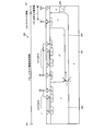
- FIG. 23 is a circuit diagram showing a conventional high voltage IC.
- a high voltage IC 200 shown in FIG. 23 is a circuit for driving the first and second IGBTs 101 and 102 constituting one phase of the power conversion bridge circuit.
- the first and second IGBTs 101 and 102 are connected in series between a high-voltage main power supply (positive electrode side) Vdc and a ground potential GND on the negative electrode side of the main power supply.
- the VS terminal is connected to a connection point 105 between the first IGBT 101 and the second IGBT 102.
- a connection point 105 is an output point of the bridge circuit configured by the first and second IGBTs 101 and 102.
- the high voltage IC 200 generally includes a high side drive circuit 110, a low side drive circuit (not shown), a level shifter 115, and a control circuit 116.
- the high side drive circuit 110 includes a gate drive circuit 111, a level shift resistor 119, and the like.
- the gate drive circuit 111 is configured such that a high-side p-channel MOSFET (insulated gate field effect transistor, hereinafter referred to as PMOS) 112 and a low-side n-channel MOSFET (hereinafter referred to as NMOS) 113 are complementary. It consists of a connected CMOS (complementary MOS) circuit.
- Reference numerals 103, 104, and 117 denote FWDs (reflux diodes).
- the control circuit 116 operates based on the ground potential GND, and generates a low-side level on / off signal for turning on / off the first IGBT 101 and a low-side level on / off signal for turning on / off the second IGBT 102. To do.
- the level shifter 115 converts the low-side level on / off signal generated by the control circuit 116 into a high-side level on / off signal input to the gate of the first IGBT 101.
- the control circuit 116 generates a low-side level on / off signal for turning on / off the first IGBT 101.
- the low-side level on / off signal is converted into a high-side level on / off signal by the level shifter 115 and then input to the high-side drive circuit 110.
- the high side drive circuit 110 operates at a potential between the intermediate potential VS and the power supply potential VB with the intermediate potential VS as a reference potential.
- the power supply potential VB is higher than the intermediate potential VS by about 15V, for example.
- the ON / OFF signal input from the control circuit 116 to the high side drive circuit 110 is input to the gate of the first IGBT 101 on the high side via the NOT circuit and the gate drive circuit 111 at the subsequent stage.
- the first IGBT 101 is turned on / off based on an on / off signal from the control circuit 116.
- the intermediate potential VS applied to the VS terminal varies between 0V and Vdc.
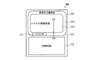
- FIG. 24 is a plan view schematically showing a planar structure of a conventional high voltage IC.
- FIG. 25 is a cross-sectional view showing a cross-sectional structure taken along section line AA-AA ′ of FIG.
- the p-type bulk substrate 201 includes a high-side drive circuit region 210 in which a high-side drive circuit is disposed, a high-breakdown-voltage isolation region 215 surrounding the high-side drive circuit region 210, and a high-breakdown-voltage isolation region.
- a low side region 216 surrounding 215 is provided.
- a level shifter 115 is disposed in the high breakdown voltage isolation region 215.
- the low side region 216 is a portion excluding the high side drive circuit region 210 and the portion of the high breakdown voltage isolation region 215 where the level shifter 115 is formed.
- a control circuit 116 is disposed in the low side region 216.
- the high side drive circuit region 210 is separated from the low side region 216 by the high breakdown voltage isolation region 215, and a higher potential of 600 V or more can be applied than the low side region 216.
- an n ⁇ diffusion region 202 is selectively formed on the surface layer of the p-type bulk substrate 201.
- the n ⁇ diffusion region 202 is provided from the high side drive circuit region 210 to the high breakdown voltage isolation region 215.
- a high side drive circuit is formed in the high side drive circuit region 210.
- a lateral PMOS 212 and a lateral NMOS 213 constituting a gate driving circuit are formed on the surface layer of the n ⁇ diffusion region 202.
- the NMOS 213 is formed in the p ⁇ diffusion region 203 provided in the surface layer of the n ⁇ diffusion region 202. Further, a p ⁇ region 204 is provided in the low side region 216 outside the n ⁇ diffusion region 202 on the surface layer of the p-type bulk substrate 201.
- a ground potential GND is applied to p type bulk substrate 201 and p ⁇ region (hereinafter referred to as p ⁇ GND region) 204.
- High side power supply potential VB is applied to n ⁇ diffusion region 202.
- Intermediate potential VS is applied to p ⁇ diffusion region 203.
- a high potential gate drive circuit unit and a level shift circuit unit are provided on the same other conductive semiconductor substrate, and at least one lateral MOSFET is formed in the high potential gate drive circuit unit.
- a device has been proposed that has a buried insulating film for suppressing parasitic elements, selectively in a direction parallel to the main surface of the semiconductor substrate and below the source and drain regions of the lateral MOSFET (for example, the following patents) Reference 1).
- An sgPMOS transistor is provided as an electrostatic protection circuit connected between the input / output terminal and the ground terminal.
- the transistor has a source and a gate connected to the input / output terminal, and a drain connected to the ground terminal.
- the drain of the transistor has a double diffusion structure including a first P-type drain diffusion layer and a second P-type drain diffusion layer (see, for example, Patent Document 2 below).
- the following devices have been proposed as another high voltage IC. It includes a p ⁇ semiconductor substrate in which a high breakdown voltage element region in which a high breakdown voltage element is formed and a low breakdown voltage element region in which a low breakdown voltage element is formed are defined. An n + buried diffusion layer and an n ⁇ epitaxial layer are formed on the p ⁇ semiconductor substrate (see, for example, Patent Document 3 (paragraph 0003 and FIG. 5) below).
- the parasitic pnp bipolar transistor 118 including the p ⁇ diffusion region 203, the n ⁇ diffusion region 202 and the p type bulk substrate 201 is provided in the high side drive circuit region 210. It is formed.
- the base, emitter, and collector of the parasitic pnp bipolar transistor 118 are connected to the VB terminal, the VS terminal, and the GND terminal, respectively.
- the parasitic pnp bipolar transistor 118 does not operate. However, when the power supply potential VB is lowered by 0.6 V or more, which is the diffusion potential of the silicon pn junction, from the intermediate potential VS due to the negative voltage surge, that is, a potential relationship of VB ⁇ (VS ⁇ 0.6 [V]) is obtained. In this case, the parasitic pnp bipolar transistor 118 is turned on. As a result, a large current flows between the VS terminal to which a high voltage (up to Vdc on the high potential side potential) is applied and the GND terminal, and thus the high voltage IC 200 may be destroyed due to heat generated by the large current.
- Non-Patent Document 2 In order to avoid such breakdown due to surge, normally, as proposed in Non-Patent Document 2, a bypass connected between the VB terminal and the VS terminal as an external component outside the p-type bulk substrate 201. A capacitor is placed. However, there is a problem that the bypass capacitor cannot be arranged due to layout design and cost restrictions, or that a sufficient effect cannot be obtained if the bypass capacitor is arranged at a position away from the high voltage IC 200 due to layout design restrictions. .
- An object of the present invention is to provide a semiconductor device that can prevent a breakdown due to a surge in order to solve the problems caused by the above-described conventional technology.
- a semiconductor device has the following characteristics.
- a second conductive type first semiconductor region to which a first potential is applied is provided on a surface layer of the first conductive type semiconductor layer.
- a second semiconductor region of a first conductivity type to which a second potential is applied is provided inside the first semiconductor region.
- the first semiconductor region and the second semiconductor region are provided with circuits that operate at a potential between the first potential that is higher than the second potential, with the second potential as a reference potential.
- An insulated gate field effect transistor having a gate electrode provided via a gate insulating film on the surface of the region sandwiched between the source region and the drain region is provided.
- the threshold voltage of the insulated gate field effect transistor is -0.1V to -0.6V.
- the source region and the gate electrode are electrically connected to the first semiconductor region.
- the drain region is electrically connected to the second semiconductor region.
- the semiconductor device according to the present invention further includes a conductor opposed to the opposite side of the gate electrode with respect to the gate insulating film via the insulator.
- the conductor is electrically connected to the drain region.
- the semiconductor device according to the present invention is characterized in that, in the above-described invention, the insulator is made of a high dielectric material.
- the semiconductor device according to the present invention is characterized in that, in the above-described invention, the insulator is made of zirconium oxide, hafnium oxide or lanthanum oxide.
- the gate and the source are electrically connected to the VB electrode to which the power supply potential VB of the high side drive circuit is applied, and the VS electrode to which the intermediate potential VS serving as the reference potential of the high side drive circuit is applied.
- a clamping PMOS insulated gate type field effect transistor
- the power supply potential VB can be suppressed from being lower than the intermediate potential VS by 0.6 V or more, which is the diffusion potential of the silicon pn junction.
- the operation of the parasitic pnp bipolar transistor due to a negative voltage surge can be suppressed in a high voltage IC manufactured by a self-isolation IC process using a p-type bulk substrate. For this reason, it is possible to prevent a large current from flowing between the VS terminal to which a high voltage (high potential side potential of Vdc) is applied and the GND terminal.
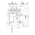
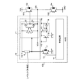
- FIG. 1 is a circuit diagram illustrating the semiconductor device according to the first embodiment.
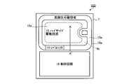
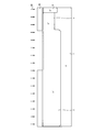
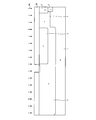
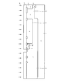
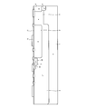
- FIG. 2 is a plan view schematically showing a planar structure of the semiconductor device according to the first embodiment.
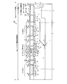
- FIG. 3 is a cross-sectional view showing a cross-sectional structure taken along section line A-A ′ of FIG.
- FIG. 4 is a cross-sectional view illustrating a state in the middle of manufacturing the semiconductor device according to the first embodiment.
- FIG. 5 is a cross-sectional view illustrating the semiconductor device according to the first embodiment in the middle of manufacturing.
- FIG. 6 is a cross-sectional view showing a state in the middle of manufacturing the semiconductor device according to the first embodiment.
- FIG. 7 is a cross-sectional view illustrating a state in the middle of manufacturing the semiconductor device according to the first embodiment.
- FIG. 8 is a cross-sectional view illustrating the semiconductor device according to the first embodiment in the middle of manufacturing.
- FIG. 9 is a cross-sectional view illustrating the semiconductor device according to the first embodiment in the middle of manufacturing.
- FIG. 10 is a cross-sectional view illustrating the semiconductor device according to the first embodiment in the middle of manufacturing.
- FIG. 11 is a cross-sectional view illustrating the semiconductor device according to the first embodiment in the middle of manufacturing.
- FIG. 12 is a cross-sectional view illustrating a state in the middle of manufacturing the semiconductor device according to the first embodiment.
- FIG. 13 is a cross-sectional view illustrating the semiconductor device according to the first embodiment in the middle of manufacturing.
- FIG. 14 is a cross-sectional view illustrating a state in the middle of manufacturing the semiconductor device according to the first embodiment.
- FIG. 15 is a cross-sectional view illustrating the semiconductor device according to the first embodiment in the middle of manufacturing.
- FIG. 16 is a cross-sectional view illustrating the semiconductor device according to the first embodiment in the middle of its manufacture.
- FIG. 17 is a cross-sectional view illustrating a state in the middle of manufacturing the semiconductor device according to the first embodiment.
- FIG. 18 is a circuit diagram of the semiconductor device according to the second embodiment.
- FIG. 19 is a plan view schematically showing a cross-sectional structure of the semiconductor device according to the second embodiment.
- FIG. 20 is a characteristic diagram showing electrical characteristics of the p-channel MOSFET for clamping.
- FIG. 20 is a characteristic diagram showing electrical characteristics of the p-channel MOSFET for clamping.
- FIG. 21 is a characteristic diagram showing electrical characteristics when the p-channel MOSFET for clamping is on.
- FIG. 22 is a characteristic diagram illustrating electrical characteristics of the semiconductor device according to the example when a negative voltage surge is applied.
- FIG. 23 is a circuit diagram showing a conventional high voltage IC.
- FIG. 24 is a plan view schematically showing a planar structure of a conventional high voltage IC.
- FIG. 25 is a cross-sectional view showing a cross-sectional structure taken along section line AA-AA ′ of FIG.
- FIG. 1 is a circuit diagram illustrating the semiconductor device according to the first embodiment.
- the semiconductor device according to the first embodiment shown in FIG. 1 is a high voltage IC 100 that drives the first and second IGBTs 101 and 102 constituting one phase of a power conversion bridge circuit (main circuit).
- a high voltage IC 100 includes a high side drive circuit 10, a low side drive circuit (not shown), a clamp enhancement type p-channel MOSFET (hereinafter referred to as a clamp PMOS) 14, a level shifter 15, and a control.
- a circuit 16 is provided.
- the high side drive circuit 10 includes a gate drive circuit 11, a NOT circuit, a level shift resistor 19, and the like.
- the first and second IGBTs 101 and 102 are connected in series between a high-voltage main power supply (positive electrode side) Vdc and a ground potential GND on the negative electrode side of the main power supply.
- the VS terminal is connected to a connection point 105 between the first IGBT 101 and the second IGBT 102.
- the connection point 105 is an output point of the bridge circuit for power conversion composed of the first and second IGBTs 101 and 102, and is connected to a motor as a load, for example.
- the intermediate potential VS applied to the VS terminal is turned on / off complementarily between the first IGBT 101 and the second IGBT 102, thereby causing the high potential side potential of the main power supply Vdc (for example, It rises and falls repeatedly between about 400V) and the low potential side potential (ground potential GND), and fluctuates between 0V and several hundred volts.
- the power supply potential VB is about 15V higher than the intermediate potential VS and about 415V higher than the substrate potential (ground potential GND).
- the high-side drive circuit 10 operates at a potential between the intermediate potential VS and the power supply potential VB using the potential (intermediate potential) VS applied to the VS terminal as a reference potential, and drives the first IGBT 101 on the high side.
- the high side drive circuit 10 uses the voltage drop of the level shift resistor 19 as a signal, and sends an ON / OFF signal to the gate of the first IGBT 101 on the high side via the NOT circuit and the gate drive circuit 11 at the subsequent stage. input.
- the gate drive circuit 11 is composed of a CMOS circuit in which a high-side p-channel MOSFET (PMOS) 12 and a low-side n-channel MOSFET (NMOS) 13 are connected so as to complement each other. Specifically, the source of the PMOS 12 is connected to the VB terminal, and the drain of the PMOS 12 is connected to the drain of the NMOS 13. The source of the NMOS 13 is connected to the VS terminal. A connection point between the PMOS 12 and the NMOS 13 is connected to the gate of the first IGBT 101.
- PMOS high-side p-channel MOSFET
- NMOS low-side n-channel MOSFET
- a clamping PMOS 14 is connected between the VB terminal and the VS terminal. Specifically, the source and gate of the clamping PMOS 14 are connected to the VB terminal. The drain of the clamping PMOS 14 is connected to the VS terminal.
- the threshold voltage of the clamping PMOS 14 is about ⁇ 0.1V to ⁇ 0.6V.
- the withstand voltage of the clamping PMOS 14 is preferably 15 V or more.
- the threshold voltage is a gate voltage when the channel is changed from the weak inversion state to the strong inversion state when the gate voltage is increased or decreased from 0V.
- the control circuit 16 operates with the ground potential GND as a reference, and generates a low-side level on / off signal for turning on / off the first IGBT 101 and a low-side level on / off signal for turning on / off the second IGBT 102. To do.
- the level shifter 15 converts the low-side level on / off signal generated by the control circuit 16 into a high-side level on / off signal input to the gate of the first IGBT 101.
- Reference numerals 103, 104, and 17 denote FWDs (reflux diodes).
- the high voltage IC 100 is manufactured by, for example, an IC process using a self-separation technique on a p-type bulk substrate.
- the planar structure of the high voltage IC 100 will be described.
- FIG. 2 is a plan view schematically showing a planar structure of the semiconductor device according to the first embodiment.
- a high-side drive circuit region 10a in which the high-side drive circuit 10 is disposed a high-voltage isolation region 15a that ensures the breakdown voltage of the high-side drive circuit 10, A low side region 16a surrounding the isolation region 15a is provided.
- a high breakdown voltage isolation region 15a is disposed so as to surround the high side drive circuit region 10a.
- the high side drive circuit region 10a is separated from the low side region 16a by the high breakdown voltage isolation region 15a, and a higher potential of 600 V or more can be applied than the low side region 16a.
- the VB electrode 4b is disposed so as to surround the high side drive circuit 10 near the boundary between the high side drive circuit region 10a and the high breakdown voltage isolation region 15a.
- a VB electrode and a VS electrode are selectively disposed according to the design conditions of the high voltage IC 100.
- a level shifter 15 is disposed in the high breakdown voltage isolation region 15a.
- the low side region 16a is a portion excluding the high side drive circuit region 10a and the portion of the high breakdown voltage isolation region 15a where the level shifter 15 is formed.
- a control circuit 16 is disposed in the low side region 16a.
- the level shifter 15 can also be formed in the low side region 16a.
- FIG. 3 is a cross-sectional view showing a cross-sectional structure taken along section line AA ′ of FIG.
- the high voltage IC 100 has an element isolation structure manufactured on a p-type bulk substrate 1 by a self-isolation IC process.
- an n ⁇ diffusion region 2 is selectively formed on the surface layer of the p-type bulk substrate 1 by a self-isolation IC process.
- the n ⁇ diffusion region 2 is provided in the high side drive circuit region 10a.
- the diffusion depth of the n ⁇ diffusion region 2 may be about 10 ⁇ m, for example.
- a p diffusion region 3 is selectively provided on the surface layer of the n ⁇ diffusion region 2.
- a high side drive circuit 10 is provided in the n ⁇ diffusion region 2 and the p diffusion region 3.
- a clamping PMOS 14 is provided in the n ⁇ diffusion region 2.
- FIG. 3 shows a lateral p-channel MOSFET (PMOS) 12 and a lateral n-channel MOSFET (NMOS) 13 constituting the gate drive circuit 11 among the components of the high-side drive circuit 10.
- the n - diffusion region 2 n - the power source potential VB is applied from the electrically connected VB electrode 2b through the n + high concentration region 2a which is provided in the diffusion region 2.
- Intermediate potential VS (potential at connection point 105) is applied to p diffusion region 3 from VS electrode 3 b electrically connected via p + high concentration region 3 a provided inside p diffusion region 3. .
- the PMOS 12 is formed in the surface layer of the n ⁇ diffusion region 2.
- the PMOS 12 includes a p + source region 21, a p + drain region 22, a gate insulating film 23, a gate electrode 24, a source electrode 25 and a drain electrode 26.
- the p + source region 21 and the p + drain region 22 are provided apart from each other inside the n ⁇ diffusion region 2.
- the diffusion depths of the p + source region 21 and the p + drain region 22 are shallower than the diffusion depth of the p diffusion region 3.
- the gate electrode 24 is provided on the surface of the portion of the n ⁇ diffusion region 2 sandwiched between the p + source region 21 and the p + drain region 22 via the gate insulating film 23.
- the source electrode 25 and the drain electrode 26 are electrically connected to the p + source region 21 and the p + drain region 22, respectively.
- the source electrode 25 is connected to the VB electrode 2b by, for example, aluminum wiring.
- the NMOS 13 is formed in the surface layer of the p diffusion region 3.
- the NMOS 13 includes an n + source region 31, an n + drain region 32, a gate insulating film 33, a gate electrode 34, a source electrode 35 and a drain electrode 36.
- the n + source region 31 and the n + drain region 32 are provided in the p diffusion region 3 so as to be separated from each other.
- the gate electrode 34 is provided on the surface of the portion of the p diffusion region 3 sandwiched between the n + source region 31 and the n + drain region 32 via the gate insulating film 33.
- the source electrode 35 and the drain electrode 36 are electrically connected to the n + source region 31 and the n + drain region 32, respectively.
- the source electrode 35 is connected to the VS electrode 3b by, for example, aluminum wiring.
- the clamping PMOS 14 is formed in the surface layer of the n ⁇ diffusion region 2.
- the clamping PMOS 14 includes a p + source region 41, a p + drain region 42, a p drain drift region 43, an n ⁇ channel region 44, a gate insulating film 45, a gate electrode 46, a source electrode 47 and a drain electrode 48.
- the p + source region 41 and the p + drain region 42 are provided apart from each other inside the n ⁇ diffusion region 2.
- the diffusion depths of the p + source region 41 and the p + drain region 42 are shallower than the diffusion depth of the p diffusion region 3.
- the p drain drift region 43 is provided inside the n ⁇ diffusion region 2 so as to cover the p + drain region 42.
- the n ⁇ channel region 44 is provided between the p + source region 41 and the p drain drift region 43.
- the gate electrode 46 is provided on the surface of the portion of the n ⁇ diffusion region 2 sandwiched between the p + source region 41 and the p + drain region 42 via the gate insulating film 45.
- the source electrode 47 and the drain electrode 48 are electrically connected to the p + source region 41 and the p + drain region 42, respectively.
- the gate electrode 46 and the source electrode 47 are connected to the VB electrode 2b by, for example, aluminum wiring.
- the drain electrode 48 is connected to the VS electrode 3b by, for example, aluminum wiring.
- the channel length L and the channel width W of the clamping PMOS 14 may be 1.7 ⁇ m and 25000 ⁇ m, respectively.
- the channel length L of the clamping PMOS 14 is the shortest distance between the p + source region 41 and the p drain drift region 43.
- the channel width W of the clamping PMOS 14 is the width of the channel portion in the direction orthogonal to the channel length L.
- the clamping PMOS 14 is illustrated between the PMOS 12 and the NMOS 13, but the clamping PMOS 14 is disposed in the high side drive circuit region 10 a and is electrically connected between the VB terminal and the VS terminal. It only has to be. Further, the effect of the present invention can be obtained as the arrangement area of the clamping PMOS 14 is larger.
- the surface layer of the p-type bulk substrate 1, n - the outside of the diffusion region 2, for example, the n - diffusion region 4 is provided - n shallow depth than the diffusion region 2.
- the n ⁇ diffusion region 4 is in contact with the n ⁇ diffusion region 2 and surrounds the periphery of the n ⁇ diffusion region 2.
- the n - diffusion region 4, n - the power source potential VB is applied from the electrically connected VB electrode 4b through the diffusion region 4 inside the n + high concentration region 4a.
- the n + high concentration region 4a and the VB electrode 4b surround the high side drive circuit region 10a. From the n ⁇ diffusion region 2 to the outer end of the n + high concentration region 4a is the high side drive circuit region 10a.
- n of p-type bulk substrate 1 of the surface layer - on the outside of the diffusion region 4 n - surrounds the diffusion regions 4 and n - are provided regions 5 - p in contact with the diffusion region 4.
- the n - Inside the region 5, n - - diffusion region 4 and p p region 6 is provided at the boundary between the region 5 - diffusion region 4 p.
- the p ⁇ region (hereinafter referred to as “p ⁇ GND region”) 5 and the p region (hereinafter referred to as “pGND region”) 6 are electrically connected via a p + high concentration region (not shown) inside the pGND region 6.
- the ground potential GND is applied from the grounded GND electrode 5b.
- the p ⁇ GND region 5 and the pGND region 6 have a function of fixing the p-type bulk substrate 1 to the ground potential GND.
- N ⁇ diffusion region 4, p ⁇ GND region 5 and pGND region 6 constitute high breakdown voltage isolation region 15 a.
- the high breakdown voltage isolation region 15a extends from the outer end of the n + high concentration region 4a to the outer end of the p ⁇ GND region 5.
- the distance T from the outer end of the n + high concentration region 4a to the inner end of the pGND region 6 is about 100 ⁇ m when the breakdown voltage is 600V, and is about 200 ⁇ m when the breakdown voltage is 1200V.
- Reference numeral 7 denotes a local insulating film such as LOCOS (Local Oxidation of Silicon).
- Reference numeral 8 denotes an interlayer insulating film such as BPSG (Boro Phospho Silicate Glass).
- Reference numeral 9 denotes a passivation film made of a silicon nitride film (Si 3 N 4 film) or the like.
- the high voltage IC 100 is manufactured by an IC process (self-separation type IC process) using a self-separation technique as described later. Therefore, a parasitic pnp bipolar transistor 18 having the p diffusion region 3 as an emitter, the n ⁇ diffusion region 2 as a base, and the p-type bulk substrate 1 as a collector is formed in the high side drive circuit region 10a. The base, emitter, and collector of the parasitic pnp bipolar transistor 18 are connected to the VB terminal, the VS terminal, and the GND terminal, respectively.
- FIG. 4 are cross-sectional views illustrating a state in the middle of manufacturing the semiconductor device according to the first embodiment.
- a p-type bulk substrate 1 made of silicon having a specific resistance of, for example, about 300 ⁇ cm is prepared.
- a resist mask 51 is formed on the surface of the p-type bulk substrate 1 to expose a portion corresponding to the formation region of the n ⁇ diffusion region 2.
- a first ion implantation 61 of an n-type impurity such as phosphorus (P) is performed using the resist mask 51 as a mask.
- a dotted line near the surface of the p-type bulk substrate 1 represents the n-type impurity implanted with the first ion 61 (the same applies to FIGS. 5 and 6).
- the acceleration voltage and the dose amount of the first ion implantation 61 may be, for example, about 50 keV and about 2.0 ⁇ 10 13 / cm 2 , respectively.
- a resist mask 52 is formed on the surface of the p-type bulk substrate 1 to expose a portion corresponding to the formation region of the n ⁇ diffusion region 4.
- a second ion implantation 62 of n-type impurities such as phosphorus is performed using the resist mask 52 as a mask.
- the acceleration voltage and the dose amount of the second ion implantation 62 may be, for example, about 50 keV and about 4.0 ⁇ 10 12 / cm 2 , respectively.
- a dotted line in the vicinity of the surface of the p-type bulk substrate 1 (a dotted line smaller than a dotted line indicating the n-type impurity implanted with the first ions 61) represents the n-type impurity implanted with the second ions 62 (FIG. 5). The same applies to 6).
- a resist mask 53 is formed on the surface of the p-type bulk substrate 1 to expose a portion corresponding to the formation region of the p ⁇ GND region 5.
- a third ion implantation 63 of a p-type impurity such as boron (B) is performed using the resist mask 53 as a mask.
- the acceleration voltage and the dose amount of the third ion implantation 63 may be, for example, about 50 keV and about 3.0 ⁇ 10 12 / cm 2 , respectively.
- a dotted line in the vicinity of the surface of the p-type bulk substrate 1 (a dotted line that is coarser than the dotted line indicating the n-type impurity implanted in the first and second ions 61 and 62) represents the p-type impurity implanted in the third ion implantation 63.
- a heat treatment at a temperature of about 1200 ° C. is performed for about 300 minutes in, for example, a nitrogen (N 2 ) atmosphere, and the n-type ions 61 to 63 implanted into the p-type bulk substrate 1 are first to third ions 61 to 63.
- the type impurity and the p-type impurity are thermally diffused.
- a resist mask 54 is formed on the surface of the p-type bulk substrate 1 on which the n ⁇ diffusion region 2 is formed (hereinafter simply referred to as the surface), and the formation of the pGND region 6. The part corresponding to the region is exposed.
- a fourth ion implantation 64 of a p-type impurity such as boron is performed using the resist mask 54 as a mask.
- the acceleration voltage and the dose amount of the fourth ion implantation 64 may be, for example, about 50 keV and about 4.0 ⁇ 10 13 / cm 2 , respectively.
- the dotted line near the surface of the p ⁇ GND region 5 represents the p-type impurity implanted by the fourth ion implantation 64 (the same applies to FIG. 9).
- a resist mask 55 is formed on the surface of the p-type bulk substrate 1 to expose a portion corresponding to the formation region of the p diffusion region 3.
- a fifth ion implantation 65 of a p-type impurity such as boron is performed using the resist mask 55 as a mask.
- the acceleration voltage and the dose amount of the fifth ion implantation 65 may be, for example, about 50 keV and about 5.0 ⁇ 10 13 / cm 2 , respectively.
- a dotted line in the vicinity of the surface of the n ⁇ diffusion region 2 (a dotted line coarser than a dotted line indicating the p-type impurity implanted by the fourth ion 64) represents the p-type impurity implanted by the fifth ion implantation 65.
- a heat treatment at a temperature of about 1150 ° C. is performed for about 240 minutes in a nitrogen atmosphere, and the p-type impurities implanted into the p-type bulk substrate 1 by the fourth and fifth ions 64 and 65 are heated.
- p diffusion region 3 and pGND region 6 are formed.
- a resist mask 56 is formed on the surface of the p-type bulk substrate 1, and a portion corresponding to the formation region of the p drain drift region 43 of the clamping PMOS 14 is exposed.
- a sixth ion implantation 66 of a p-type impurity such as boron is performed using the resist mask 56 as a mask.
- the acceleration voltage and the dose amount of the sixth ion implantation 66 may be, for example, about 50 keV and about 4.0 ⁇ 10 13 / cm 2 , respectively.
- the dotted line near the surface of the n ⁇ diffusion region 2 represents the p-type impurity implanted by the sixth ion implantation 66.
- a heat treatment at a temperature of about 1150 ° C. is performed for about 90 minutes in a nitrogen atmosphere, and the p-type impurity implanted into the sixth ion implantation 66 is thermally diffused into the p-type bulk substrate 1.
- the p drain drift region 43 is formed.
- a local oxidation film 7 is formed by performing thermal oxidation treatment at a temperature of about 1000 ° C. for about 90 minutes in an oxygen (O 2 ) atmosphere.
- a resist mask 57 is formed on the surface of the p-type bulk substrate 1, and a portion corresponding to the formation region of the n ⁇ channel region 44 of the clamping PMOS 14 is exposed.
- a seventh ion implantation 67 of a p-type impurity such as boron is performed using the resist mask 57 as a mask.
- the acceleration voltage and the dose amount of the seventh ion implantation 67 may be, for example, about 120 keV and about 1.0 ⁇ 10 12 / cm 2 , respectively.
- the dotted line near the surface of the n ⁇ diffusion region 2 represents the p-type impurity implanted with the seventh ion implantation 67.
- a silicon oxide film 71 having a thickness of 50 mm is formed on the surface of the p-type bulk substrate 1 by thermal oxidation in an oxygen atmosphere.
- the silicon oxide film 71 becomes the gate insulating films 23, 33 and 45.
- a 3000-thick doped polysilicon film 72 is formed on the silicon oxide film 71 by low pressure CVD (chemical vapor deposition) and patterned. As a result, gate electrodes 24, 34, and 46 are formed.
- a resist mask 58 is formed on the surface of the p-type bulk substrate 1 to form the p + source region 41 and p + drain region 42 of the clamping PMOS 14 and the p + high concentration region 3a. A portion corresponding to the formation region is exposed.
- an eighth ion implantation 68 of a p-type impurity such as boron is performed using the resist mask 58 as a mask.
- the acceleration voltage and the dose amount of the eighth ion implantation 68 may be about 65 keV and about 3.0 ⁇ 10 15 / cm 2 , respectively.
- the eighth ion implantation 68 is also performed in a portion corresponding to a p + high concentration region forming region (not shown) inside the pGND region 6.
- dotted lines near the surfaces of the n ⁇ diffusion region 2, the p diffusion region 3 and the p drain drift region 43 represent the p-type impurity implanted by the eighth ion implantation 68 (the same applies to FIG. 17).
- a resist mask 59 is formed on the surface of the p-type bulk substrate 1 to correspond to the formation regions of the n + high concentration region 2a and the n + high concentration region 4a. Expose the area to be exposed.
- a ninth ion implantation 69 of an n-type impurity such as arsenic (As) is performed using the resist mask 59 as a mask.
- the acceleration voltage and the dose amount of the ninth ion implantation 69 may be, for example, about 65 keV and about 4.0 ⁇ 10 15 / cm 2 , respectively.
- dotted lines near the surface of the n ⁇ diffusion region 2 and n ⁇ diffusion region 4 are the n type implanted by the ninth ion implantation 69. It represents an impurity.
- n ⁇ channel region 44, p + source region 41, p + drain region 42, p + high concentration region 3a, n + high concentration region 2a, n + high concentration region 4a, and A p + high concentration region (not shown) inside the pGND region 6 is formed.
- an interlayer insulating film 8 having a thickness of 1.0 ⁇ m is deposited by the CVD method.
- the interlayer insulating film 8 is selectively removed by photolithography to form a plurality of contact holes.
- an aluminum (Al) film having a thickness of 1.0 ⁇ m is deposited on the interlayer insulating film 8.
- the aluminum film is formed inside the p + source region 41, the p + drain region 42, the p + high concentration region 3a, the n + high concentration region 2a, the n + high concentration region 4a, and the pGND region 6 through each contact hole. It is in contact with a p + high concentration region (not shown).
- the aluminum film is patterned to form a source electrode 47, a drain electrode 48, a VB electrode 2b, a VS electrode 3b, a GND electrode 5b, and an aluminum wiring (not shown).
- a high-voltage IC 100 shown in FIGS. 1 to 3 is completed by forming a passivation film 9 having a thickness of 1.0 ⁇ m by plasma CVD.
- the PMOS 12, NMOS 13, resistor, capacitor, and the like are formed on the p-type bulk substrate 1 on which the clamping PMOS 14 is formed by adding a general manufacturing process to the method for manufacturing the high voltage IC 100 described above.
- the timing for forming the PMOS 12, NMOS 13, resistor, capacitor (capacitance), and the like can be variously changed according to the design conditions of the high voltage IC 100.
- Each region of the PMOS 12 and the NMOS 13 may be formed together with a region having the same diffusion depth and impurity concentration of the clamping PMOS 14, for example.
- the control circuit 16 generates a low-side level on / off signal.
- the low-side level on / off signal is input to the high-side drive circuit 10 via the level shifter 15.
- the high side drive circuit 10 operates at a potential between the intermediate potential VS and the power supply potential VB with the intermediate potential VS as a reference potential.
- the potential applied to the VS terminal varies from 0V to several hundred volts.
- the power supply potential VB is higher than the intermediate potential VS by about 15V, for example.
- the ON / OFF signal input to the high side drive circuit 10 is input to the gate of the first IGBT 101 on the high side via the NOT circuit and the gate drive circuit 11 at the subsequent stage.
- the first IGBT 101 is turned on / off based on an on / off signal from the control circuit 16. Since the power supply potential VB is higher than the intermediate potential VS in the normal operation of the high voltage IC 100, the parasitic pnp bipolar transistor 18 does not operate. Further, since the power supply potential VB is higher than the intermediate potential VS, the clamping PMOS 14 is in an off state, and no current flows through the clamping PMOS 14.
- the clamping PMOS 14 is turned on, and from the VS electrode 3 b via the clamping PMOS 14.
- a current flows to the VB electrodes 2b and 4b.
- the base current flowing between the base and the emitter of the parasitic pnp bipolar transistor 18 can be reduced.
- the current flowing in the clamping PMOS 14 is mainly a parasitic pn formed by the p + drain region 42 and the n ⁇ diffusion region 2 as the back gate. This is because the diode is turned on.
- the clamping PMOS 14 is assumed to be a PMOS having the same structure (hereinafter referred to as reverse clamping PMOS) having the p + source region 41 as a drain, the p + drain region 42 as a source, and the n ⁇ diffusion region 2 as a back gate. . Since the channel has bidirectionality, even if it is a PMOS for reverse clamping, a drain current can flow from the source to the drain by applying a gate voltage lower than the threshold voltage to the source as in a normal MOSFET. it can.
- the reverse clamping PMOS has a drain, a gate, and a back gate connected to the VB terminal and a source connected to the VS terminal. Therefore, when the power supply potential VB is lower than the intermediate potential VS by the absolute value of the threshold voltage of the clamping PMOS 14, a voltage higher than the absolute value of the threshold voltage is applied between the gate and the source of the reverse clamping PMOS. Therefore, the reverse clamping PMOS is turned on, and the channel current of the clamping PMOS 14 flows.
- the threshold voltage of the reverse clamping PMOS is higher than the threshold voltage of the clamping PMOS 14 due to the back gate effect. Has also declined.
- the gate and the source are electrically connected to the VB electrode to which the power supply potential VB of the high-side drive circuit is applied, and the intermediate becomes the reference potential of the high-side drive circuit.
- a negative voltage surge is applied by providing a high-side drive circuit area with a clamping PMOS with a threshold voltage of about -0.1 V to -0.6 V in which the drain electrode is electrically connected to the VS electrode to which the potential VS is applied. Current can be passed through the clamping PMOS.
- the operation of the parasitic pnp bipolar transistor due to a negative voltage surge can be suppressed in a high voltage IC manufactured by a self-isolation IC process using a p-type bulk substrate. Therefore, it is possible to prevent a large current from flowing between the VS terminal to which a high voltage (up to Vdc high potential side potential) is applied and the GND terminal, and to prevent the high breakdown voltage IC from being destroyed. be able to.
- a high-breakdown voltage IC is manufactured at low cost by only ion implantation and thermal diffusion by a self-isolation IC process that does not require a special element isolation process, using an inexpensive bulk substrate. Can do. Further, there is no need to provide a bypass capacitor connected between the VB terminal and the VS terminal as an external component. Thereby, an inexpensive high voltage IC can be provided.
- the clamping PMOS can be formed in the high-side driving circuit area together with the PMOS and the NMOS constituting the gate driving circuit. For this reason, the effect which avoids the destruction by a negative voltage surge can be improved.
- a clamping PMOS can be formed in the high-side drive circuit region, even when a bypass capacitor connected as an external component is not provided between the VB terminal and the VS terminal or when the distance is long. The effect of avoiding the breakdown due to the negative voltage surge can be improved, and the degree of freedom in layout design is increased.
- FIG. 18 is a circuit diagram of the semiconductor device according to the second embodiment.
- FIG. 19 is a plan view schematically showing a cross-sectional structure of the semiconductor device according to the second embodiment.
- the planar structure of the semiconductor device according to the second embodiment is the same as the planar structure of the semiconductor device according to the first embodiment. That is, FIG. 19 shows a cross-sectional structure taken along section line AA ′ of FIG.
- the high voltage IC 120 according to the second embodiment is different from the high voltage IC 100 according to the first embodiment in that a bypass capacitor 81 is connected between the VB terminal and the VS terminal (FIG. 18).
- the bypass capacitor 81 is formed in the vicinity of the gate electrode 46 of the clamping PMOS 14 in the interlayer insulating film 8.
- the bypass capacitor 81 includes a gate electrode 46 of the clamping PMOS 14, an insulating film 83, and a conductor (hereinafter referred to as a capacitor electrode) 82.
- the capacitor electrode 82 is provided on the opposite side to the gate insulating film 45 side of the gate electrode 46 via an insulating film 83.
- the capacitor electrode 82 is connected to the VS electrode 3b by, for example, aluminum wiring. That is, the capacitor electrode 82 is electrically connected to the p + drain region 42 of the clamping PMOS 14 in a low resistance state.
- the insulating film 83 is preferably made of a high dielectric material such as zirconium oxide (ZrO 2 ), hafnium oxide (HfO 2 ), or lanthanum oxide (La 2 O 3 ).
- the reason is that the capacity of the bypass capacitor 81 can be increased.
- the thickness of the insulating film 83 may be, for example, 250 mm.
- the same effect as that of the first embodiment can be obtained.
- the semiconductor device according to the second embodiment is highly effective in a device having a configuration in which a bypass capacitor is not provided therein, such as an intelligent power module (IPM).
- IPM intelligent power module
- a bypass capacitor can be formed in the high-side drive circuit region together with the PMOS and NMOS constituting the gate drive circuit. For this reason, the effect which avoids destruction by a negative voltage surge can be improved rather than the case where a bypass capacitor is connected as an external component.
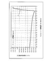
- FIG. 20 is a characteristic diagram showing electrical characteristics of the p-channel MOSFET for clamping.
- FIG. 20 shows the relationship between the drain current and the drain-source voltage (VS terminal-VB terminal voltage) when the gate-source voltage Vgs of the clamping PMOS 14 is 0V.
- the threshold voltage of the clamping PMOS 14 was set to ⁇ 0.15V.
- the area of the parasitic pnp bipolar transistor 18 was 0.2 mm 2 in the case of a general high voltage IC.
- the drain-source voltage is less than the absolute value of the threshold voltage of the clamping PMOS 14, that is, less than 0.15 V, no current flows between the drain and source of the clamping PMOS 14.
- the drain potential of the clamping PMOS 14 becomes 0.15 V or more higher than the source potential, an inversion layer is formed in the n ⁇ channel region 44, and a current flows between the drain and source of the clamping PMOS 14.
- the current that flows when the drain-source voltage is 0.0 V to 0.6 V is the channel current of the clamping PMOS 14 (the drain-source voltage 0.6 V is indicated by an arrow 91).
- the current that flows when the drain-source voltage is 0.6 V or more is the current that flows in the parasitic pn diode formed by the p + drain region 42 and the n ⁇ diffusion region 2 of the clamping PMOS 14.
- FIG. 21 is a characteristic diagram showing electrical characteristics when the p-channel MOSFET for clamping is on.
- FIG. 22 is a characteristic diagram illustrating electrical characteristics of the semiconductor device according to the example when a negative voltage surge is applied.
- FIG. 21 is a characteristic diagram showing electrical characteristics when the p-channel MOSFET for clamping is on.
- FIG. 22 is a characteristic diagram illustrating electrical characteristics of the semiconductor device according to the example when a negative voltage surge is applied.
- the drain electrode 48 of the clamping PMOS 14 is connected to the VS electrode 3b, and the source electrode 47 is connected to the VB electrode 2b.
- the present invention can be variously modified.
- the dimensions of each part are variously set according to required specifications.
- the semiconductor device according to the present invention is useful for a power semiconductor device used for a power conversion device such as an inverter or a power supply device such as various industrial machines.
Landscapes
- Metal-Oxide And Bipolar Metal-Oxide Semiconductor Integrated Circuits (AREA)
- Semiconductor Integrated Circuits (AREA)
- Insulated Gate Type Field-Effect Transistor (AREA)
Abstract
p型バルク基板(1)のおもて面側に設けられたn-拡散領域(2)の表面層には、p拡散領域(3)が選択的に設けられる。n-拡散領域(2)には、電源電位(VB)が印加され、ハイサイド駆動回路のPMOS(12)と、クランプ用PMOS(14)とが配置される。p拡散領域(3)には、中間電位(VS)が印加され、ハイサイド駆動回路のNMOS(13)が配置される。ハイサイド駆動回路は、中間電位(VS)を基準電位として、中間電位(VS)と電源電位(VB)との間の電位で動作する。クランプ用PMOS(14)の閾値電圧は-0.1V~-0.6V程度である。クランプ用PMOS(14)のp+ソース領域(41)およびゲート電極(46)はVB電極(2b)に接続される。クランプ用PMOS(14)のp+ドレイン領域(42)はVS電極(3b)に接続される。これにより、サージによる破壊を防止することができる。
Description
この発明は、半導体装置に関する。
従来、産業用インバータにおいて電力変換用ブリッジ回路を構成するIGBT(絶縁ゲート型バイポーラトランジスタ)等のスイッチング素子のゲート駆動に用いる半導体素子として、入力側と出力側とを電気的に絶縁するトランスやフォトカプラが公知である。また、近年、主に低容量のインバータ用途において、低コスト化のために、入力側と出力側とを電気的に絶縁しない高耐圧IC(HVIC)が用いられている(例えば、下記非特許文献1,2参照)。
従来の高耐圧ICの回路構成について説明する。図23は、従来の高耐圧ICを示す回路図である。図23に示す高耐圧IC200は、電力変換用ブリッジ回路の一相分を構成する第1,2IGBT101,102を駆動する回路である。第1,2IGBT101,102は、高圧の主電源(正極側)Vdcと、この主電源の負極側であるグランド電位GNDとの間に直列に接続される。VS端子は、第1IGBT101と第2IGBT102との接続点105に接続される。接続点105は、第1,2IGBT101,102で構成されるブリッジ回路の出力点である。
高耐圧IC200は、一般的に、ハイサイド駆動回路110、ローサイド駆動回路(不図示)、レベルシフタ115、制御回路116を備える。ハイサイド駆動回路110は、ゲート駆動回路111、レベルシフト抵抗119などを備える。ゲート駆動回路111は、ハイサイド側のpチャネルMOSFET(絶縁ゲート型電界効果トランジスタ、以下、PMOSとする)112と、ローサイド側のnチャネルMOSFET(以下、NMOSとする)113とが相補うように接続されたCMOS(相補型MOS)回路よりなる。符号103,104,117はFWD(還流ダイオード)である。
制御回路116は、グランド電位GNDを基準として動作し、第1IGBT101をオン・オフするためのローサイドレベルのオン・オフ信号、および第2IGBT102をオン・オフするためのローサイドレベルのオン・オフ信号を生成する。レベルシフタ115は、制御回路116によって生成されたローサイドレベルのオン・オフ信号を、第1IGBT101のゲートに入力されるハイサイドレベルのオン・オフ信号に変換する。
ハイサイド側の第1IGBT101を駆動する場合の高耐圧IC200の動作について説明する。制御回路116によって第1IGBT101をオン・オフするためのローサイドレベルのオン・オフ信号が生成される。このローサイドレベルのオン・オフ信号は、レベルシフタ115によりハイサイドレベルのオン・オフ信号に変換された後、ハイサイド駆動回路110に入力される。ハイサイド駆動回路110は、中間電位VSを基準電位として、中間電位VSと電源電位VBとの間の電位で動作する。電源電位VBは、中間電位VSよりも例えば15V程度高くなっている。
制御回路116からハイサイド駆動回路110に入力されたオン・オフ信号は、NOT回路およびその後段のゲート駆動回路111を介してハイサイド側の第1IGBT101のゲートに入力される。第1IGBT101は、制御回路116からのオン・オフ信号に基づいてオン・オフされる。高耐圧IC200の動作中、VS端子に印加される中間電位VSは0VからVdcまでの間で変動する。
このような高耐圧IC200を低コストで作製(製造)する方法として、安価なバルク基板を用いることができ、かつ特別な素子分離プロセスを必要としない自己分離技術を用いたICプロセスが適している。自己分離型ICプロセスによって作製された高耐圧IC200の構造について説明する。図24は、従来の高耐圧ICの平面構造を模式的に示す平面図である。図25は、図24の切断線AA-AA’における断面構造を示す断面図である。
図24,25に示すように、p型バルク基板201には、ハイサイド駆動回路が配置されたハイサイド駆動回路領域210、ハイサイド駆動回路領域210を囲む高耐圧分離領域215、高耐圧分離領域215を囲むローサイド領域216が設けられている。高耐圧分離領域215には、レベルシフタ115が配置される。ローサイド領域216は、ハイサイド駆動回路領域210と、高耐圧分離領域215の、レベルシフタ115が形成された部分とを除いた部分である。ローサイド領域216には、制御回路116が配置される。ハイサイド駆動回路領域210は、高耐圧分離領域215によってローサイド領域216と分離され、ローサイド領域216よりも600V以上の高電位が印加可能となっている。
p型バルク基板201の表面層には、n-拡散領域202が選択的に形成されている。n-拡散領域202は、ハイサイド駆動回路領域210から高耐圧分離領域215にわたって設けられている。n-拡散領域202には、ハイサイド駆動回路領域210においてハイサイド駆動回路が形成されている。具体的には、n-拡散領域202の表面層には、ゲート駆動回路を構成する横型のPMOS212および横型のNMOS213が形成されている。
NMOS213は、n-拡散領域202の表面層に設けられたp-拡散領域203に形成される。また、p型バルク基板201の表面層の、n-拡散領域202の外側には、ローサイド領域216内にp-領域204が設けられている。p型バルク基板201およびp-領域(以下、p-GND領域とする)204にはグランド電位GNDが印加される。n-拡散領域202には、ハイサイド電源電位VBが印加される。p-拡散領域203には中間電位VSが印加される。
このような高耐圧ICとして、高電位ゲート駆動回路部と、レベルシフト回路部とを同一の他導電型半導体基板上に備え、前記高電位ゲート駆動回路部には少なくとも一つの横型MOSFETが形成され、前記半導体基板の主面に平行方向に選択的に、かつ前記横型MOSFETのソース領域およびドレイン領域の下方に、寄生素子抑制用の埋め込み絶縁膜を有する装置が提案されている(例えば、下記特許文献1参照。)。
また、別の高耐圧ICとして、次の装置が提案されている。入出力端子と接地端子の間に接続された静電保護回路としてのsgPMOSトランジスタを備えている。トランジスタはソースとゲートが入出力端子に接続され、ドレインが接地端子に接続されている。トランジスタのドレインは第1P型ドレイン拡散層と第2P型ドレイン拡散層からなる二重拡散構造を備えている(例えば、下記特許文献2参照。)。
また、別の高耐圧ICとして、次の装置が提案されている。高耐圧素子が形成された高耐圧素子領域と、低耐圧素子が形成された低耐圧素子領域とが規定されたp-半導体基板を含む。p-半導体基板の上には、n+埋込み拡散層、n-エピタキシャル層が形成されている(例えば、下記特許文献3(第0003段落、第5図)参照。)。
ティー・フジヒラ(T.FUJIHIRA)、外4名、プロポーザル オブ ニュー インターコネクション テクニック フォア ベリー ハイ-ボルテージ IC’s(Proposal of New Interconnection Technique for Very High-Voltage IC’s)、ジャパニーズ ジャーナル オブ アプライド フィジクス(Japanese Journal of Applied Physics)、1996年11月、第35巻(第1版)、第11号、p.5655-5663
ジョナサン・アダムス(Jonathan Adams)、"コントロールIC用ブートストラップ回路部品の選定"、[online]、インターナショナル・レクティファイアー・ジャパン株式会社(International Rectifier Japan)、[平成24年9月24日検索]、インターネット<http://www.irf-japan.com/technical-info/designtp/dt98-2j.pdf>
しかしながら、自己分離型ICプロセスによって作製された高耐圧IC200では、ハイサイド駆動回路領域210内に、p-拡散領域203、n-拡散領域202およびp型バルク基板201からなる寄生pnpバイポーラトランジスタ118が形成される。寄生pnpバイポーラトランジスタ118のベース、エミッタおよびコレクタは、それぞれ、VB端子、VS端子、GND端子に接続された状態となる。
高耐圧IC200の通常動作において、電源電位VBは中間電位VSよりも高いため、寄生pnpバイポーラトランジスタ118は動作しない。しかし、負電圧サージにより電源電位VBが中間電位VSよりもシリコンpn接合の拡散電位である0.6V以上低下した場合、すなわちVB<(VS-0.6[V])の電位関係になった場合、寄生pnpバイポーラトランジスタ118がオン状態となる。これにより、高電圧(~Vdcの高電位側電位)が印加されたVS端子とGND端子との間に大電流が流れるため、大電流による発熱によって高耐圧IC200が破壊される虞がある。
このようなサージによる破壊を回避するため、通常、上記非特許文献2で提案されるように、p型バルク基板201の外部に外付け部品としてVB端子とVS端子との間に接続されたバイパスコンデンサが配置される。しかしながら、レイアウト設計やコスト上の制約によりバイパスコンデンサを配置することができなかったり、レイアウト設計の制約により高耐圧IC200から離れた位置に配置されることで十分に効果が得られないという問題がある。
この発明は、上述した従来技術による問題点を解消するため、サージによる破壊を防止することができる半導体装置を提供することを目的とする。
上述した課題を解決し、本発明の目的を達成するため、この発明にかかる半導体装置は、次の特徴を有する。第1導電型の半導体層の表面層に、第1電位が印加される第2導電型の第1半導体領域が設けられている。前記第1半導体領域の内部に、第2電位が印加される第1導電型の第2半導体領域が設けられている。前記第1半導体領域および前記第2半導体領域に、前記第2電位を基準電位とし、前記第2電位よりも高い前記第1電位との間の電位で動作する回路が設けられている。前記第1半導体領域の内部に選択的に設けられた第1導電型のソース領域、前記第1半導体領域の内部に選択的に設けられた第1導電型のドレイン領域、および、前記第1半導体領域の、前記ソース領域と前記ドレイン領域とに挟まれた部分の表面にゲート絶縁膜を介して設けられたゲート電極を有する絶縁ゲート型電界効果トランジスタが設けられている。前記絶縁ゲート型電界効果トランジスタの閾値電圧は-0.1V~-0.6Vである。前記ソース領域および前記ゲート電極は前記第1半導体領域に電気的に接続されている。前記ドレイン領域は前記第2半導体領域に電気的に接続されている。
また、この発明にかかる半導体装置は、上述した発明において、絶縁体を介して、前記ゲート電極の前記ゲート絶縁膜側に対して反対側に対向する導電体をさらに備える。前記導電体は、前記ドレイン領域に電気的に接続されていることを特徴とする。
また、この発明にかかる半導体装置は、上述した発明において、前記絶縁体は、高誘電体材料でできていることを特徴とする。
また、この発明にかかる半導体装置は、上述した発明において、前記絶縁体は、酸化ジルコニウム、酸化ハフニウムまたは酸化ランタンでできていることを特徴とする。
上述した発明によれば、ハイサイド駆動回路の電源電位VBが印加されるVB電極にゲートおよびソースが電気的に接続され、ハイサイド駆動回路の基準電位となる中間電位VSが印加されるVS電極にドレインが電気的に接続されたクランプ用PMOS(絶縁ゲート型電界効果トランジスタ)をハイサイド駆動回路領域(第1半導体領域)に設けることで、負電圧サージが印加されたときにクランプ用PMOSに電流を流すことができる。これにより、負電圧サージが印加されたときに電源電位VBが中間電位VSよりもシリコンpn接合の拡散電位である0.6V以上低下することを抑制することができる。したがって、p型バルク基板を用いて自己分離型ICプロセスによって作製した高耐圧ICにおいて、負電圧サージによる寄生pnpバイポーラトランジスタの動作を抑制することができる。このため、高電圧(Vdcの高電位側電位)が印加されたVS端子とGND端子との間に大電流が流れることを防止することができる。
本発明にかかる半導体装置によれば、サージによる破壊を防止することができるという効果を奏する。
以下に添付図面を参照して、この発明にかかる半導体装置の好適な実施の形態を詳細に説明する。本明細書および添付図面においては、nまたはpを冠記した層や領域では、それぞれ電子または正孔が多数キャリアであることを意味する。また、nやpに付す+および-は、それぞれそれが付されていない層や領域よりも高不純物濃度および低不純物濃度であることを意味する。なお、以下の実施の形態の説明および添付図面において、同様の構成には同一の符号を付し、重複する説明を省略する。
(実施の形態1)
実施の形態1にかかる半導体装置の構造について説明する。図1は、実施の形態1にかかる半導体装置を示す回路図である。図1に示す実施の形態1にかかる半導体装置は、電力変換用ブリッジ回路(主回路)の一相分を構成する第1,2IGBT101,102を駆動する高耐圧IC100である。図1に示すように、高耐圧IC100は、ハイサイド駆動回路10、ローサイド駆動回路(不図示)、クランプ用のエンハンストメント型pチャネルMOSFET(以下、クランプ用PMOSとする)14、レベルシフタ15、制御回路16を備える。
実施の形態1にかかる半導体装置の構造について説明する。図1は、実施の形態1にかかる半導体装置を示す回路図である。図1に示す実施の形態1にかかる半導体装置は、電力変換用ブリッジ回路(主回路)の一相分を構成する第1,2IGBT101,102を駆動する高耐圧IC100である。図1に示すように、高耐圧IC100は、ハイサイド駆動回路10、ローサイド駆動回路(不図示)、クランプ用のエンハンストメント型pチャネルMOSFET(以下、クランプ用PMOSとする)14、レベルシフタ15、制御回路16を備える。
ハイサイド駆動回路10は、ゲート駆動回路11、NOT回路、レベルシフト抵抗19などを備える。第1,2IGBT101,102は、高圧の主電源(正極側)Vdcと、この主電源の負極側であるグランド電位GNDとの間に直列に接続されている。VS端子は、第1IGBT101と第2IGBT102との接続点105に接続される。接続点105は、第1,2IGBT101,102で構成される電力変換用ブリッジ回路の出力点であり、例えば負荷であるモータなどが接続される。
高耐圧IC100の動作中、VS端子に印加される中間電位VSは、第1IGBT101と第2IGBT102とが相補にオン・オフ(on・off)されることによって、主電源Vdcの高電位側電位(例えば400V程度)と低電位側電位(グランド電位GND)との間で上昇および下降を繰り返し、0Vから数百Vまでの間で変動する。電源電位VBは、中間電位VSよりも15V程度高くなっており、基板電位(グランド電位GND)よりも415V程度高くなっている。
ハイサイド駆動回路10は、VS端子に印加される電位(中間電位)VSを基準電位として、中間電位VSと電源電位VBとの間の電位で動作し、ハイサイド側の第1IGBT101を駆動する。具体的には、ハイサイド駆動回路10は、レベルシフト抵抗19の電圧降下を信号として、NOT回路およびその後段のゲート駆動回路11を介してハイサイド側の第1IGBT101のゲートにオン・オフ信号を入力する。
ゲート駆動回路11は、ハイサイド側のpチャネルMOSFET(PMOS)12と、ローサイド側のnチャネルMOSFET(NMOS)13とが相補うように接続されたCMOS回路よりなる。具体的には、PMOS12のソースはVB端子に接続され、PMOS12のドレインはNMOS13のドレインに接続されている。NMOS13のソースはVS端子に接続されている。PMOS12とNMOS13との接続点は、第1IGBT101のゲートに接続されている。
また、VB端子とVS端子との間には、クランプ用PMOS14が接続されている。具体的には、クランプ用PMOS14のソースおよびゲートはVB端子に接続されている。クランプ用PMOS14のドレインは、VS端子に接続されている。クランプ用PMOS14の閾値電圧は、-0.1V~-0.6V程度である。クランプ用PMOS14の耐圧は15V以上であるのが好ましい。なお、ここでいう閾値電圧とは、ゲート電圧を0Vから上昇あるいは降下させた際に、チャネルが弱反転状態から強反転状態に変わる時のゲート電圧のことである。
制御回路16は、グランド電位GNDを基準として動作し、第1IGBT101をオン・オフするためのローサイドレベルのオン・オフ信号、および第2IGBT102をオン・オフするためのローサイドレベルのオン・オフ信号を生成する。レベルシフタ15は、制御回路16によって生成されたローサイドレベルのオン・オフ信号を、第1IGBT101のゲートに入力されるハイサイドレベルのオン・オフ信号に変換する。符号103,104,17はFWD(還流ダイオード)である。
高耐圧IC100は、例えばp型バルク基板上に自己分離技術を用いたICプロセスによって製造される。高耐圧IC100の平面構造について説明する。図2は、実施の形態1にかかる半導体装置の平面構造を模式的に示す平面図である。図2に示すように、p型バルク基板1上には、ハイサイド駆動回路10が配置されたハイサイド駆動回路領域10a、ハイサイド駆動回路10の耐圧を確保する高耐圧分離領域15a、高耐圧分離領域15aを囲むローサイド領域16aが設けられている。
ハイサイド駆動回路領域10aの周囲には、ハイサイド駆動回路領域10aを囲むように高耐圧分離領域15aが配置される。ハイサイド駆動回路領域10aは、高耐圧分離領域15aによってローサイド領域16aと分離され、ローサイド領域16aよりも600V以上の高電位が印加可能となっている。ハイサイド駆動回路領域10aには、例えばハイサイド駆動回路領域10aと高耐圧分離領域15aとの境界付近においてハイサイド駆動回路10を囲むようにVB電極4bが配置される。
ハイサイド駆動回路領域10a内には、高耐圧IC100の設計条件に応じて図示省略するVB電極およびVS電極が選択的に配置される。ハイサイド駆動回路領域10a内にVB電極およびVS電極を配置することにより、ノイズとなるキャリアを引き抜くことができる。高耐圧分離領域15aには、レベルシフタ15が配置される。ローサイド領域16aは、ハイサイド駆動回路領域10aと、高耐圧分離領域15aの、レベルシフタ15が形成された部分とを除いた部分である。ローサイド領域16aには、制御回路16が配置される。レベルシフタ15をローサイド領域16aに形成することもできる。
次に、高耐圧IC100の断面構造について説明する。図3は、図2の切断線A-A’における断面構造を示す断面図である。図3に示すように、高耐圧IC100は、p型バルク基板1に自己分離型ICプロセスによって作製された素子分離構造を有する。p型バルク基板1の表面層には、n-拡散領域2が選択的に形成されている。n-拡散領域2は、ハイサイド駆動回路領域10aに設けられている。n-拡散領域2の拡散深さは、例えば10μm程度であってもよい。n-拡散領域2の表面層には、p拡散領域3が選択的に設けられている。
n-拡散領域2およびp拡散領域3には、ハイサイド駆動回路10が設けられている。n-拡散領域2には、クランプ用PMOS14が設けられている。図3には、ハイサイド駆動回路10の構成部のうち、ゲート駆動回路11を構成する横型のpチャネルMOSFET(PMOS)12および横型のnチャネルMOSFET(NMOS)13を示す。n-拡散領域2には、n-拡散領域2の内部に設けられたn+高濃度領域2aを介して電気的に接続されたVB電極2bから電源電位VBが印加される。p拡散領域3には、p拡散領域3の内部に設けられたp+高濃度領域3aを介して電気的に接続されたVS電極3bから中間電位VS(接続点105の電位)が印加される。
具体的には、PMOS12は、n-拡散領域2の表面層に形成されている。PMOS12は、p+ソース領域21、p+ドレイン領域22、ゲート絶縁膜23、ゲート電極24、ソース電極25およびドレイン電極26を備える。p+ソース領域21およびp+ドレイン領域22は、n-拡散領域2の内部に互いに離れて設けられる。p+ソース領域21およびp+ドレイン領域22の拡散深さは、p拡散領域3の拡散深さよりも浅い。ゲート電極24は、n-拡散領域2の、p+ソース領域21とp+ドレイン領域22とに挟まれた部分の表面にゲート絶縁膜23を介して設けられている。ソース電極25およびドレイン電極26は、それぞれp+ソース領域21およびp+ドレイン領域22に電気的に接続されている。ソース電極25は、例えばアルミニウム配線によってVB電極2bに接続される。
NMOS13は、p拡散領域3の表面層に形成されている。NMOS13は、n+ソース領域31、n+ドレイン領域32、ゲート絶縁膜33、ゲート電極34、ソース電極35およびドレイン電極36を備える。n+ソース領域31およびn+ドレイン領域32は、p拡散領域3の内部に互いに離れて設けられている。ゲート電極34は、p拡散領域3の、n+ソース領域31とn+ドレイン領域32とに挟まれた部分の表面にゲート絶縁膜33を介して設けられている。ソース電極35およびドレイン電極36は、それぞれn+ソース領域31およびn+ドレイン領域32に電気的に接続されている。ソース電極35は、例えばアルミニウム配線によってVS電極3bに接続される。
クランプ用PMOS14は、n-拡散領域2の表面層に形成されている。クランプ用PMOS14は、p+ソース領域41、p+ドレイン領域42、pドレインドリフト領域43、n-チャネル領域44、ゲート絶縁膜45、ゲート電極46、ソース電極47およびドレイン電極48を備える。クランプ用PMOS14において、p+ソース領域41およびp+ドレイン領域42は、n-拡散領域2の内部に互いに離れて設けられている。p+ソース領域41およびp+ドレイン領域42の拡散深さは、p拡散領域3の拡散深さよりも浅い。pドレインドリフト領域43は、p+ドレイン領域42を覆うようにn-拡散領域2の内部に設けられている。
n-チャネル領域44は、p+ソース領域41とpドレインドリフト領域43との間に設けられている。ゲート電極46は、n-拡散領域2の、p+ソース領域41とp+ドレイン領域42とに挟まれた部分の表面にゲート絶縁膜45を介して設けられている。ソース電極47およびドレイン電極48は、それぞれp+ソース領域41およびp+ドレイン領域42に電気的に接続されている。ゲート電極46およびソース電極47は、例えばアルミニウム配線によってVB電極2bに接続される。ドレイン電極48は、例えばアルミニウム配線によってVS電極3bに接続される。
クランプ用PMOS14のチャネル長Lおよびチャネル幅Wは、それぞれ、例えば1.7μmおよび25000μmであってもよい。クランプ用PMOS14のチャネル長Lとは、p+ソース領域41とpドレインドリフト領域43との間の最短距離である。クランプ用PMOS14のチャネル幅Wは、チャネル長Lに直交する方向のチャネル部の幅である。図3では、PMOS12とNMOS13との間にクランプ用PMOS14を図示しているが、クランプ用PMOS14はハイサイド駆動回路領域10a内に配置され、VB端子とVS端子との間に電気的に接続されていればよい。また、クランプ用PMOS14の配置面積が広い程、より本発明の効果が得られる。
また、p型バルク基板1の表面層の、n-拡散領域2の外側には、例えばn-拡散領域2よりも浅い深さでn-拡散領域4が設けられている。n-拡散領域4は、n-拡散領域2に接し、かつn-拡散領域2の周囲を囲む。n-拡散領域4には、n-拡散領域4内部のn+高濃度領域4aを介して電気的に接続されたVB電極4bから電源電位VBが印加される。n+高濃度領域4aおよびVB電極4bは、ハイサイド駆動回路領域10aの周囲を囲む。n-拡散領域2から、n+高濃度領域4aの外側の端部までがハイサイド駆動回路領域10aである。
p型バルク基板1の表面層のn-拡散領域4の外側には、n-拡散領域4の周囲を囲み、かつn-拡散領域4に接するp-領域5が設けられている。n-拡散領域4およびp-領域5の内部には、n-拡散領域4とp-領域5との境界にp領域6が設けられている。p-領域(以下、p-GND領域とする)5およびp領域(以下、pGND領域とする)6には、pGND領域6内部のp+高濃度領域(不図示)を介して電気的に接続されたGND電極5bからグランド電位GNDが印加される。p-GND領域5およびpGND領域6は、p型バルク基板1をグランド電位GNDに固定する機能を有する。
n-拡散領域4、p-GND領域5およびpGND領域6は、高耐圧分離領域15aを構成する。具体的には、n+高濃度領域4aの外側の端部からp-GND領域5の外側の端部までが高耐圧分離領域15aである。n+高濃度領域4aの外側の端部からpGND領域6の内側の端部までの距離Tは、耐圧600Vである場合に100μm程度であり、耐圧1200Vである場合に200μm程度である。
n+高濃度領域4aの外側の端部から外側の、シフトレジスタ(不図示)が形成された部分を除いた部分がローサイド領域16aである。符号7はLOCOS(Local Oxidation of Silicon)などの局部絶縁膜である。符号8はBPSG(Boro Phospho Silicate Glass)等の層間絶縁膜である。符号9はシリコン窒化膜(Si3N4膜)などからなるパッシベーション膜である。
また、高耐圧IC100は、後述するように自己分離技術を用いたICプロセス(自己分離型ICプロセス)によって作製される。このため、ハイサイド駆動回路領域10a内には、p拡散領域3をエミッタとし、n-拡散領域2をベースとし、p型バルク基板1をコレクタとする寄生pnpバイポーラトランジスタ18が形成される。寄生pnpバイポーラトランジスタ18のベース、エミッタおよびコレクタは、それぞれ、VB端子、VS端子、GND端子に接続された状態となる。
次に、高耐圧IC100の製造方法について説明する。主に、クランプ用PMOS14の製造工程について説明する。図4~17は、実施の形態1にかかる半導体装置の製造途中の状態を示す断面図である。まず、図4に示すように、比抵抗が例えば300Ωcm程度のシリコンからなるp型バルク基板1を用意する。次に、p型バルク基板1の表面にレジストマスク51を形成し、n-拡散領域2の形成領域に対応する部分を露出させる。
次に、レジストマスク51をマスクとして例えばリン(P)などのn型不純物の第1イオン注入61を行う。図4において、p型バルク基板1表面近傍の点線は、第1イオン注入61されたn型不純物をあらわしている(図5,6においても同様)。第1イオン注入61の加速電圧およびドーズ量は、それぞれ、例えば50keV程度および2.0×10¹³/cm2程度であってもよい。
次に、図5に示すように、レジストマスク51の除去後、p型バルク基板1の表面にレジストマスク52を形成し、n-拡散領域4の形成領域に対応する部分を露出させる。次に、レジストマスク52をマスクとして例えばリンなどのn型不純物の第2イオン注入62を行う。第2イオン注入62の加速電圧およびドーズ量は、それぞれ、例えば50keV程度および4.0×10¹²/cm2程度であってもよい。図5において、p型バルク基板1表面近傍の点線(第1イオン注入61されたn型不純物を示す点線よりも細かい点線)は、第2イオン注入62されたn型不純物をあらわしている(図6においても同様)。
次に、図6に示すように、レジストマスク52の除去後、p型バルク基板1の表面にレジストマスク53を形成し、p-GND領域5の形成領域に対応する部分を露出させる。次に、レジストマスク53をマスクとして例えばボロン(B)などのp型不純物の第3イオン注入63を行う。第3イオン注入63の加速電圧およびドーズ量は、それぞれ、例えば50keV程度および3.0×10¹²/cm2程度であってもよい。
図6において、p型バルク基板1表面近傍の点線(第1,2イオン注入61,62されたn型不純物を示す点線よりも粗い点線)は、第3イオン注入63されたp型不純物をあらわしている。次に、レジストマスク53の除去後、例えば窒素(N2)雰囲気下において1200℃程度の温度の熱処理を300分程度行い、p型バルク基板1に第1~3イオン注入61~63されたn型不純物およびp型不純物を熱拡散させる。これにより、図7に示すように、n-拡散領域2、n-拡散領域4およびp-GND領域5が形成される。
次に、図8に示すように、p型バルク基板1の、n-拡散領域2が形成された側の表面(以下、単に表面とする)にレジストマスク54を形成し、pGND領域6の形成領域に対応する部分を露出させる。次に、レジストマスク54をマスクとして例えばボロンなどのp型不純物の第4イオン注入64を行う。第4イオン注入64の加速電圧およびドーズ量は、それぞれ、例えば50keV程度および4.0×10¹³/cm2程度であってもよい。図8において、p-GND領域5表面近傍の点線は、第4イオン注入64されたp型不純物をあらわしている(図9においても同様)。
次に、図9に示すように、レジストマスク54の除去後、p型バルク基板1の表面にレジストマスク55を形成し、p拡散領域3の形成領域に対応する部分を露出させる。次に、レジストマスク55をマスクとして例えばボロンなどのp型不純物の第5イオン注入65を行う。第5イオン注入65の加速電圧およびドーズ量は、それぞれ、例えば50keV程度および5.0×10¹³/cm2程度であってもよい。
図9において、n-拡散領域2表面近傍の点線(第4イオン注入64されたp型不純物を示す点線よりも粗い点線)は、第5イオン注入65されたp型不純物をあらわしている。次に、レジストマスク55の除去後、例えば窒素雰囲気下において1150℃程度の温度の熱処理を240分程度行い、p型バルク基板1に第4,5イオン注入64,65されたp型不純物を熱拡散させる。これにより、図10に示すように、p拡散領域3およびpGND領域6が形成される。
次に、図11に示すように、p型バルク基板1の表面にレジストマスク56を形成し、クランプ用PMOS14のpドレインドリフト領域43の形成領域に対応する部分を露出させる。次に、レジストマスク56をマスクとして例えばボロンなどのp型不純物の第6イオン注入66を行う。第6イオン注入66の加速電圧およびドーズ量は、それぞれ、例えば50keV程度および4.0×10¹³/cm2程度であってもよい。図11において、n-拡散領域2表面近傍の点線は、第6イオン注入66されたp型不純物をあらわしている。
次に、レジストマスク56の除去後、例えば窒素雰囲気下において1150℃程度の温度の熱処理を90分程度行い、p型バルク基板1に第6イオン注入66されたp型不純物を熱拡散させる。これにより、図12に示すように、pドレインドリフト領域43が形成される。次に、図13に示すように、酸素(O2)雰囲気下に1000℃程度の温度の熱酸化処理を90分程度行い、局部絶縁膜7を形成する。
次に、図14に示すように、p型バルク基板1の表面にレジストマスク57を形成し、クランプ用PMOS14のn-チャネル領域44の形成領域に対応する部分を露出させる。次に、レジストマスク57をマスクとして例えばボロンなどのp型不純物の第7イオン注入67を行う。第7イオン注入67の加速電圧およびドーズ量は、それぞれ、例えば120keV程度および1.0×10¹²/cm2程度であってもよい。図14において、n-拡散領域2表面近傍の点線は、第7イオン注入67されたp型不純物をあらわしている。第7イオン注入67されたp型不純物によって、n-拡散領域2の、n-チャネル領域44の形成領域に対応する部分のn型不純物濃度が低くなる。
次に、図15に示すように、酸素雰囲気下で熱酸化することにより、p型バルク基板1の表面に厚さ50Åのシリコン酸化膜71を形成する。シリコン酸化膜71は、ゲート絶縁膜23,33,45となる。次に、減圧CVD(化学気相成長)法により、シリコン酸化膜71上に厚さ3000Åのドープドポリシリコン膜72を形成してパターニングする。これにより、ゲート電極24,34,46が形成される。
次に、図16に示すように、p型バルク基板1の表面にレジストマスク58を形成し、クランプ用PMOS14のp+ソース領域41およびp+ドレイン領域42の形成領域とp+高濃度領域3aの形成領域とに対応する部分を露出させる。次に、レジストマスク58をマスクとして例えばボロンなどのp型不純物の第8イオン注入68を行う。第8イオン注入68の加速電圧およびドーズ量は、それぞれ、例えば65keV程度および3.0×10¹⁵/cm2程度であってもよい。このとき、pGND領域6内部の図示省略するp+高濃度領域の形成領域に対応する部分にも第8イオン注入68を行う。図16において、n-拡散領域2、p拡散領域3およびpドレインドリフト領域43の表面近傍の点線は、第8イオン注入68されたp型不純物をあらわしている(図17においても同様)。
次に、図17に示すように、レジストマスク58の除去後、p型バルク基板1の表面にレジストマスク59を形成し、n+高濃度領域2aおよびn+高濃度領域4aの形成領域に対応する部分を露出させる。次に、レジストマスク59をマスクとして例えば砒素(As)などのn型不純物の第9イオン注入69を行う。第9イオン注入69の加速電圧およびドーズ量は、それぞれ、例えば65keV程度および4.0×10¹⁵/cm2程度であってもよい。図17において、n-拡散領域2およびn-拡散領域4の表面近傍の点線(第8イオン注入68されたp型不純物を示す点線よりも細かい点線)は、第9イオン注入69されたn型不純物をあらわしている。
次に、レジストマスク59の除去後、熱処理を行い、p型バルク基板1に第7~9イオン注入67~69されたn型不純物およびp型不純物を熱拡散させる。これにより、図3に示すように、n-チャネル領域44、p+ソース領域41、p+ドレイン領域42、p+高濃度領域3a、n+高濃度領域2a、n+高濃度領域4a、および、pGND領域6内部の図示省略するp+高濃度領域が形成される。次に、CVD法により厚さ1.0μmの層間絶縁膜8を堆積する。次に、フォトリソグラフィにより層間絶縁膜8を選択的に除去し、複数のコンタクトホールを形成する。
次に、層間絶縁膜8上に例えば厚さ1.0μmのアルミニウム(Al)膜を堆積する。アルミニウム膜は、各コンタクトホールを介してp+ソース領域41、p+ドレイン領域42、p+高濃度領域3a、n+高濃度領域2a、n+高濃度領域4a、および、pGND領域6内部の図示省略するp+高濃度領域に接する。次に、アルミニウム膜をパターニングし、ソース電極47、ドレイン電極48、VB電極2b、VS電極3b、GND電極5b、およびアルミニウム配線(不図示)を形成する。
次に、プラズマCVD法により厚さ1.0μmのパッシベーション膜9を形成することにより、図1~3に示す高耐圧IC100が完成する。PMOS12、NMOS13、抵抗、コンデンサなどは、上述した高耐圧IC100の製造方法に一般的な製造工程を追加することによって、クランプ用PMOS14の形成されたp型バルク基板1上に形成される。PMOS12、NMOS13、抵抗、キャパシタ(容量)などを形成するタイミングは、高耐圧IC100の設計条件に合わせて種々変更可能である。PMOS12およびNMOS13の各領域は、例えばクランプ用PMOS14の、拡散深さおよび不純物濃度が等しい領域とともに形成してもよい。
次に、ハイサイド側の第1IGBT101を駆動する場合の高耐圧IC100の動作について説明する。制御回路16によってローサイドレベルのオン・オフ信号が生成される。このローサイドレベルのオン・オフ信号は、レベルシフタ15を介してハイサイド駆動回路10に入力される。ハイサイド駆動回路10は、中間電位VSを基準電位として、中間電位VSと電源電位VBとの間の電位で動作する。高耐圧IC100の動作中、VS端子に印加される電位は0Vから数百Vまで変化する。電源電位VBは、中間電位VSよりも例えば15V程度高くなっている。
ハイサイド駆動回路10に入力されたオン・オフ信号は、NOT回路およびその後段のゲート駆動回路11を介してハイサイド側の第1IGBT101のゲートに入力される。第1IGBT101は、制御回路16からのオン・オフ信号に基づいてオン・オフされる。高耐圧IC100の通常動作において電源電位VBが中間電位VSよりも高いため、寄生pnpバイポーラトランジスタ18は動作しない。また、電源電位VBが中間電位VSよりも高いため、クランプ用PMOS14はオフ状態であり、クランプ用PMOS14に電流は流れない。
一方、負電圧サージが印加され、電源電位VBが中間電位VSよりもクランプ用PMOS14の閾値電圧の絶対値以上低下した場合、クランプ用PMOS14がオン状態となり、クランプ用PMOS14を介してVS電極3bからVB電極2b,4bへ電流が流れる。これにより、寄生pnpバイポーラトランジスタ18のベース-エミッタ間に流れるベース電流を低減することができる。電源電位VBが中間電位VSよりも0.6V以上低下した場合にクランプ用PMOS14に流れる電流は、主に、p+ドレイン領域42とバックゲートであるn-拡散領域2とによって形成される寄生pnダイオードがターンオンすることによるものである。
また、電源電位VBが中間電位VSよりもクランプ用PMOS14の閾値電圧の絶対値以上0.6V以下低下した場合にクランプ用PMOS14に流れる電流は、クランプ用PMOS14のチャネル電流によるものである。クランプ用PMOS14のチャネル電流が流れる理由について説明する。クランプ用PMOS14を、p+ソース領域41をドレインとし、p+ドレイン領域42をソースとし、n-拡散領域2をバックゲートとした同一構造のPMOS(以下、逆クランプ用PMOSとする)と仮定する。チャネルは双方向性を有するため、逆クランプ用PMOSであっても、通常のMOSFETと同様にソースに対して閾値電圧以下のゲート電圧を印加することによりソースからドレインへとドレイン電流を流すことができる。
高耐圧IC100において逆クランプ用PMOSは、ドレイン、ゲート、およびバックゲートがVB端子に接続され、ソースがVS端子に接続された状態となっている。したがって、電源電位VBが中間電位VSよりもクランプ用PMOS14の閾値電圧の絶対値以上低下した場合、逆クランプ用PMOSのゲート-ソース間に閾値電圧の絶対値以上の電圧が印加されることとなるため、逆クランプ用PMOSはオン状態となり、クランプ用PMOS14のチャネル電流が流れる。このとき、電源電位VBの低下により逆クランプ用PMOSのバックゲートであるn-拡散領域2の電位が低下するため、逆クランプ用PMOSの閾値電圧は、バックゲート効果によりクランプ用PMOS14の閾値電圧よりも低下している。
以上、説明したように、実施の形態1によれば、ハイサイド駆動回路の電源電位VBが印加されるVB電極にゲートおよびソースが電気的に接続され、ハイサイド駆動回路の基準電位となる中間電位VSが印加されるVS電極にドレイン電極が電気的に接続された閾値電圧-0.1V~-0.6V程度のクランプ用PMOSをハイサイド駆動回路領域に設けることで、負電圧サージが印加されたときにクランプ用PMOSに電流を流すことができる。これにより、負電圧サージが印加された場合に、電源電位VBが中間電位VSよりもシリコンpn接合の拡散電位である0.6V以上低下することを抑制することができる。したがって、p型バルク基板を用いて自己分離型ICプロセスによって作製した高耐圧ICにおいて、負電圧サージによる寄生pnpバイポーラトランジスタの動作を抑制することができる。このため、高電圧(~Vdcの高電位側電位)が印加されたVS端子とGND端子との間に大電流が流れることを防止することができ、高耐圧ICが破壊されることを防止することができる。
また、実施の形態1によれば、安価なバルク基板を用いて、特別な素子分離プロセスを必要としない自己分離型ICプロセスによってイオン注入および熱拡散のみによって低コストで高耐圧ICを作製することができる。また、外付け部品として、VB端子とVS端子との間に接続するバイパスコンデンサを設ける必要がなくなる。これによって、安価な高耐圧ICを提供することができる。
また、実施の形態1によれば、ゲート駆動回路を構成するPMOSやNMOSとともに、ハイサイド駆動回路領域内にクランプ用PMOSを形成することができる。このため、負電圧サージによる破壊を回避する効果を向上させることができる。また、ハイサイド駆動回路領域内にクランプ用PMOSを形成することができるため、VB端子とVS端子との間に外付け部品として接続するバイパスコンデンサが設けられない場合や距離が離れている場合でも負電圧サージによる破壊を回避する効果を向上させることができレイアウト設計の自由度が高くなる。
(実施の形態2)
実施の形態2にかかる半導体装置の構造について説明する。図18は、実施の形態2にかかる半導体装置を示す回路図である。図19は、実施の形態2にかかる半導体装置の断面構造を模式的に示す平面図である。実施の形態2にかかる半導体装置の平面構造は、実施の形態1にかかる半導体装置の平面構造と同様である。すなわち、図19には、図2の切断線A-A’における断面構造を示す。実施の形態2にかかる高耐圧IC120が実施の形態1にかかる高耐圧IC100と異なる点は、VB端子とVS端子との間にバイパスコンデンサ81が接続されている点である(図18)。
実施の形態2にかかる半導体装置の構造について説明する。図18は、実施の形態2にかかる半導体装置を示す回路図である。図19は、実施の形態2にかかる半導体装置の断面構造を模式的に示す平面図である。実施の形態2にかかる半導体装置の平面構造は、実施の形態1にかかる半導体装置の平面構造と同様である。すなわち、図19には、図2の切断線A-A’における断面構造を示す。実施の形態2にかかる高耐圧IC120が実施の形態1にかかる高耐圧IC100と異なる点は、VB端子とVS端子との間にバイパスコンデンサ81が接続されている点である(図18)。
図19に示すように、バイパスコンデンサ81は、層間絶縁膜8内の、クランプ用PMOS14のゲート電極46付近に形成される。具体的には、バイパスコンデンサ81は、クランプ用PMOS14のゲート電極46、絶縁膜83および導電体(以下、コンデンサ電極とする)82で構成されている。コンデンサ電極82は、ゲート電極46のゲート絶縁膜45側に対して反対側に絶縁膜83を介して設けられている。また、コンデンサ電極82は、例えばアルミニウム配線によってVS電極3bに接続される。すなわち、コンデンサ電極82は、クランプ用PMOS14のp+ドレイン領域42と低抵抗な状態で電気的に接続されている。
絶縁膜83は、例えば、酸化ジルコニウム(ZrO2)、酸化ハフニウム(HfO2)または酸化ランタン(La2O3)等の高誘電体材料でできているのが望ましい。その理由は、バイパスコンデンサ81の容量を大きくすることができるからである。絶縁膜83の厚さは、例えば250Åであってもよい。バイパスコンデンサ81を設けることにより、負電圧サージが印加され、電源電位VBが中間電位VSよりもクランプ用PMOS14の閾値電圧の絶対値以上低下した場合、クランプ用PMOS14だけでなく、バイパスコンデンサ81を介してVS電極3bからVB電極2b,4bへ電流を流すことができる。
以上、説明したように、実施の形態2によれば、実施の形態1と同様の効果を得ることができる。また、実施の形態2によれば、バイパスコンデンサを設けることにより、電源電位VBが中間電位VSよりも低下することを抑制することができる。このため、実施の形態2にかかる半導体装置は、例えば、インテリジェント・パワー・モジュール(IPM)など、従来、その内部にバイパスコンデンサを設けない構成の装置において高い効果を奏する。また、実施の形態2によれば、ゲート駆動回路を構成するPMOSやNMOSとともに、ハイサイド駆動回路領域内にバイパスコンデンサを形成することができる。このため、外付け部品としてバイパスコンデンサを接続する場合よりも負電圧サージによる破壊を回避する効果を向上させることができる。
(実施例)
次に、本発明にかかる半導体装置のクランプ用PMOS14の動作について、実施の形態1にかかる高耐圧IC(以下、実施例とする)を用いて検証した。図20は、クランプ用のpチャネルMOSFETの電気的特性を示す特性図である。図20には、クランプ用PMOS14のゲート-ソース間電圧Vgsが0Vのときの、ドレイン電流と、ドレイン-ソース間電圧(VS端子-VB端子間電圧)との関係を示す。クランプ用PMOS14の閾値電圧を-0.15Vとした。寄生pnpバイポーラトランジスタ18の面積は、一般的な高耐圧ICの場合の0.2mm2とした。図20に示すように、ドレイン-ソース間電圧がクランプ用PMOS14の閾値電圧の絶対値未満、すなわち0.15V未満である場合、クランプ用PMOS14のドレイン-ソース間に電流は流れない。
次に、本発明にかかる半導体装置のクランプ用PMOS14の動作について、実施の形態1にかかる高耐圧IC(以下、実施例とする)を用いて検証した。図20は、クランプ用のpチャネルMOSFETの電気的特性を示す特性図である。図20には、クランプ用PMOS14のゲート-ソース間電圧Vgsが0Vのときの、ドレイン電流と、ドレイン-ソース間電圧(VS端子-VB端子間電圧)との関係を示す。クランプ用PMOS14の閾値電圧を-0.15Vとした。寄生pnpバイポーラトランジスタ18の面積は、一般的な高耐圧ICの場合の0.2mm2とした。図20に示すように、ドレイン-ソース間電圧がクランプ用PMOS14の閾値電圧の絶対値未満、すなわち0.15V未満である場合、クランプ用PMOS14のドレイン-ソース間に電流は流れない。
一方、クランプ用PMOS14のドレイン電位がソース電位よりも0.15V以上高くなった場合、n-チャネル領域44に反転層が形成され、クランプ用PMOS14のドレイン-ソース間に電流が流れる。ドレイン-ソース間電圧が0.0V~0.6Vのときに流れる電流は、クランプ用PMOS14のチャネル電流である(ドレイン-ソース間電圧0.6Vを矢印91で示す)。また、ドレイン-ソース間電圧が0.6V以上のときに流れる電流は、クランプ用PMOS14のp+ドレイン領域42とn-拡散領域2とによって形成される寄生pnダイオードに流れる電流である。
図21は、クランプ用のpチャネルMOSFETのオン時の電気的特性を示す特性図である。図22は、実施例にかかる半導体装置の負電圧サージ印加時の電気的特性を示す特性図である。図21の横軸のVS端子-VB端子間電圧とは、中間電位VSから電源電位VBを減じた値(=中間電位VS-電源電位VB)である。図22の縦軸のVB端子-VS端子間電圧とは、電源電位VBから中間電位VSを減じた値(=電源電位VB-中間電位VS)である。図21に示すように、従来の高耐圧IC(図23参照、以下、従来例とする)のようにクランプ用PMOS14を備えていない場合、サージ電圧が印加され寄生pnpバイポーラトランジスタ118のベース-エミッタ間に10mAのベース電流(サージ電流)が流れた場合、電源電位VBが中間電位VSよりも0.65V低くなることが確認された。したがって、図22に示すように、従来例では、電源電位VBが中間電位VSよりも0.6V以上低下することが確認された。
一方、実施の形態1にかかる高耐圧IC(実施例)においては、クランプ用PMOS14のドレイン電極48がVS電極3bに接続され、ソース電極47がVB電極2bに接続されることにより、電源電位VBが中間電位VSよりも0.15V低下したときに、クランプ用PMOS14を介してVS電極3bからVB電極2bへドレイン電流(サージ電流)が流れ、電源電位VBが中間電位VSよりも0.50Vしか低下しないことが確認された。すなわち、実施例においては、寄生pnpバイポーラトランジスタ18のベース電流を従来例よりも1/100(=1.0×10-4/1.0×10-2)に抑えることができることが確認された。したがって、実施例においては、図22に示すように、電源電位VBが中間電位VSよりも0.6V以上低下しないため、寄生pnpバイポーラトランジスタ18が動作しないことが確認された。
以上において本発明は種々変更可能であり、上述した各実施の形態において、例えば各部の寸法は要求される仕様等に応じて種々設定される。
以上のように、本発明にかかる半導体装置は、インバータなどの電力変換装置や種々の産業用機械などの電源装置などに使用されるパワー半導体装置に有用である。
1 p型バルク基板
2,4 n-拡散領域
2a,4a n+高濃度領域
2b,4b VB電極
3 p拡散領域
3a p+高濃度領域
3b VS電極
5 p-GND領域
5b GND電極
6 pGND領域
7 局部絶縁膜
8 層間絶縁膜
9 パッシベーション膜
10 ハイサイド駆動回路
10a ハイサイド駆動回路領域
11 ゲート駆動回路
12 pチャネルMOSFET(PMOS)
13 nチャネルMOSFET(NMOS)
14 クランプ用のpチャネルMOSFET(クランプ用PMOS)
15 レベルシフタ
15a 高耐圧分離領域
16 制御回路
16a ローサイド領域
17,103,104 FWD
18 寄生pnpバイポーラトランジスタ
19 レベルシフト抵抗
21,31,41 ソース領域
22,32,42 ドレイン領域
23,33,45 ゲート絶縁膜
24,34,46 ゲート電極
25,35,47 ソース電極
26,36,48 ドレイン電極
43 pドレインドリフト領域
44 チャネル領域
81 バイパスコンデンサ
82 コンデンサ電極
83 絶縁膜
100 高耐圧IC
101 第1IGBT
102 第2IGBT
105 接続点
GND グランド電位
L クランプ用PMOSのチャネル長
T n+高濃度領域の外側の端部からpGND領域の内側の端部までの距離
VB 電源電位
VS 中間電位
Vdc 主電源
2,4 n-拡散領域
2a,4a n+高濃度領域
2b,4b VB電極
3 p拡散領域
3a p+高濃度領域
3b VS電極
5 p-GND領域
5b GND電極
6 pGND領域
7 局部絶縁膜
8 層間絶縁膜
9 パッシベーション膜
10 ハイサイド駆動回路
10a ハイサイド駆動回路領域
11 ゲート駆動回路
12 pチャネルMOSFET(PMOS)
13 nチャネルMOSFET(NMOS)
14 クランプ用のpチャネルMOSFET(クランプ用PMOS)
15 レベルシフタ
15a 高耐圧分離領域
16 制御回路
16a ローサイド領域
17,103,104 FWD
18 寄生pnpバイポーラトランジスタ
19 レベルシフト抵抗
21,31,41 ソース領域
22,32,42 ドレイン領域
23,33,45 ゲート絶縁膜
24,34,46 ゲート電極
25,35,47 ソース電極
26,36,48 ドレイン電極
43 pドレインドリフト領域
44 チャネル領域
81 バイパスコンデンサ
82 コンデンサ電極
83 絶縁膜
100 高耐圧IC
101 第1IGBT
102 第2IGBT
105 接続点
GND グランド電位
L クランプ用PMOSのチャネル長
T n+高濃度領域の外側の端部からpGND領域の内側の端部までの距離
VB 電源電位
VS 中間電位
Vdc 主電源
Claims (4)
- 第1導電型の半導体層と、
前記半導体層の表面層に設けられ、第1電位が印加される第2導電型の第1半導体領域と、
前記第1半導体領域の内部に設けられ、第2電位が印加される第1導電型の第2半導体領域と、
前記第1半導体領域および前記第2半導体領域に設けられ、前記第2電位を基準電位とし、前記第2電位よりも高い前記第1電位との間の電位で動作する回路と、
前記第1半導体領域の内部に選択的に設けられた第1導電型のソース領域、前記第1半導体領域の内部に選択的に設けられた第1導電型のドレイン領域、および、前記第1半導体領域の、前記ソース領域と前記ドレイン領域とに挟まれた部分の表面にゲート絶縁膜を介して設けられたゲート電極を有する絶縁ゲート型電界効果トランジスタと、
を備え、
前記絶縁ゲート型電界効果トランジスタの閾値電圧は-0.1V~-0.6Vであり、
前記ソース領域および前記ゲート電極は前記第1半導体領域に電気的に接続され、
前記ドレイン領域は前記第2半導体領域に電気的に接続されていることを特徴とする半導体装置。 - 絶縁体を介して、前記ゲート電極の前記ゲート絶縁膜側に対して反対側に対向する導電体をさらに備え、
前記導電体は、前記ドレイン領域に電気的に接続されていることを特徴とする請求項1に記載の半導体装置。 - 前記絶縁体は、高誘電体材料でできていることを特徴とする請求項2に記載の半導体装置。
- 前記絶縁体は、酸化ジルコニウム、酸化ハフニウムまたは酸化ランタンでできていることを特徴とする請求項2または3に記載の半導体装置。
Priority Applications (3)
| Application Number | Priority Date | Filing Date | Title |
|---|---|---|---|
| JP2014540896A JPWO2014058028A1 (ja) | 2012-10-12 | 2013-10-10 | 半導体装置 |
| CN201380019814.3A CN104247005A (zh) | 2012-10-12 | 2013-10-10 | 半导体装置 |
| US14/507,138 US20150021711A1 (en) | 2012-10-12 | 2014-10-06 | Semiconductor device |
Applications Claiming Priority (2)
| Application Number | Priority Date | Filing Date | Title |
|---|---|---|---|
| JP2012-227527 | 2012-10-12 | ||
| JP2012227527 | 2012-10-12 |
Related Child Applications (1)
| Application Number | Title | Priority Date | Filing Date |
|---|---|---|---|
| US14/507,138 Continuation US20150021711A1 (en) | 2012-10-12 | 2014-10-06 | Semiconductor device |
Publications (1)
| Publication Number | Publication Date |
|---|---|
| WO2014058028A1 true WO2014058028A1 (ja) | 2014-04-17 |
Family
ID=50477493
Family Applications (1)
| Application Number | Title | Priority Date | Filing Date |
|---|---|---|---|
| PCT/JP2013/077641 Ceased WO2014058028A1 (ja) | 2012-10-12 | 2013-10-10 | 半導体装置 |
Country Status (4)
| Country | Link |
|---|---|
| US (1) | US20150021711A1 (ja) |
| JP (1) | JPWO2014058028A1 (ja) |
| CN (1) | CN104247005A (ja) |
| WO (1) | WO2014058028A1 (ja) |
Cited By (5)
| Publication number | Priority date | Publication date | Assignee | Title |
|---|---|---|---|---|
| CN105391440A (zh) * | 2014-08-25 | 2016-03-09 | 瑞萨电子株式会社 | 半导体装置、功率控制装置和电子系统 |
| JP2016042558A (ja) * | 2014-08-19 | 2016-03-31 | 富士電機株式会社 | 半導体装置 |
| JP2017022678A (ja) * | 2015-07-15 | 2017-01-26 | ルネサスエレクトロニクス株式会社 | 半導体装置および電力制御装置 |
| US9893065B2 (en) | 2015-02-18 | 2018-02-13 | Fuji Electric Co., Ltd. | Semiconductor integrated circuit |
| US10825812B2 (en) | 2016-08-12 | 2020-11-03 | Fuji Electric Co., Ltd. | Semiconductor integrated circuit |
Families Citing this family (5)
| Publication number | Priority date | Publication date | Assignee | Title |
|---|---|---|---|---|
| TWI629785B (zh) * | 2016-12-29 | 2018-07-11 | Nuvoton Technology Corporation | 高電壓積體電路的高電壓終端結構 |
| CN109427771B (zh) * | 2017-09-01 | 2020-10-30 | 无锡华润上华科技有限公司 | 一种集成电路芯片及其制作方法、栅驱动电路 |
| JP7188026B2 (ja) * | 2018-11-29 | 2022-12-13 | 富士電機株式会社 | 半導体集積回路 |
| JP7001050B2 (ja) | 2018-12-28 | 2022-01-19 | 三菱電機株式会社 | 半導体装置 |
| CN110190055A (zh) * | 2019-04-09 | 2019-08-30 | 上海华虹宏力半导体制造有限公司 | 一种栅驱动工艺的高压自屏蔽结构 |
Citations (2)
| Publication number | Priority date | Publication date | Assignee | Title |
|---|---|---|---|---|
| JPH0373567A (ja) * | 1989-08-14 | 1991-03-28 | Nec Corp | 半導体集積回路の入力保護装置 |
| JPH10125802A (ja) * | 1996-10-16 | 1998-05-15 | Sanken Electric Co Ltd | 保護素子を含む半導体回路装置 |
Family Cites Families (3)
| Publication number | Priority date | Publication date | Assignee | Title |
|---|---|---|---|---|
| US7271989B2 (en) * | 2004-06-03 | 2007-09-18 | Altera Corporation | Electrostatic discharge protection circuit |
| KR100626009B1 (ko) * | 2004-06-30 | 2006-09-20 | 삼성에스디아이 주식회사 | 박막 트랜지스터 구조체 및 이를 구비하는 평판디스플레이 장치 |
| US20130264640A1 (en) * | 2012-04-06 | 2013-10-10 | Texas Instruments Incorporated | Drain extended mos transistor having selectively silicided drain |
-
2013
- 2013-10-10 CN CN201380019814.3A patent/CN104247005A/zh active Pending
- 2013-10-10 JP JP2014540896A patent/JPWO2014058028A1/ja active Pending
- 2013-10-10 WO PCT/JP2013/077641 patent/WO2014058028A1/ja not_active Ceased
-
2014
- 2014-10-06 US US14/507,138 patent/US20150021711A1/en not_active Abandoned
Patent Citations (2)
| Publication number | Priority date | Publication date | Assignee | Title |
|---|---|---|---|---|
| JPH0373567A (ja) * | 1989-08-14 | 1991-03-28 | Nec Corp | 半導体集積回路の入力保護装置 |
| JPH10125802A (ja) * | 1996-10-16 | 1998-05-15 | Sanken Electric Co Ltd | 保護素子を含む半導体回路装置 |
Cited By (9)
| Publication number | Priority date | Publication date | Assignee | Title |
|---|---|---|---|---|
| JP2016042558A (ja) * | 2014-08-19 | 2016-03-31 | 富士電機株式会社 | 半導体装置 |
| US9608072B2 (en) | 2014-08-19 | 2017-03-28 | Fuji Electric Co., Ltd. | Semiconductor device |
| CN105391440A (zh) * | 2014-08-25 | 2016-03-09 | 瑞萨电子株式会社 | 半导体装置、功率控制装置和电子系统 |
| JP2016046693A (ja) * | 2014-08-25 | 2016-04-04 | ルネサスエレクトロニクス株式会社 | 半導体装置、電力制御装置および電子システム |
| CN105391440B (zh) * | 2014-08-25 | 2020-06-16 | 瑞萨电子株式会社 | 半导体装置、功率控制装置和电子系统 |
| US9893065B2 (en) | 2015-02-18 | 2018-02-13 | Fuji Electric Co., Ltd. | Semiconductor integrated circuit |
| JP2017022678A (ja) * | 2015-07-15 | 2017-01-26 | ルネサスエレクトロニクス株式会社 | 半導体装置および電力制御装置 |
| US10825812B2 (en) | 2016-08-12 | 2020-11-03 | Fuji Electric Co., Ltd. | Semiconductor integrated circuit |
| US11233052B2 (en) | 2016-08-12 | 2022-01-25 | Fuji Electric Co., Ltd. | Method of manufacturing semiconductor integrated circuit |
Also Published As
| Publication number | Publication date |
|---|---|
| JPWO2014058028A1 (ja) | 2016-09-05 |
| CN104247005A (zh) | 2014-12-24 |
| US20150021711A1 (en) | 2015-01-22 |
Similar Documents
| Publication | Publication Date | Title |
|---|---|---|
| WO2014058028A1 (ja) | 半導体装置 | |
| JP6008054B2 (ja) | 半導体装置 | |
| US9478543B2 (en) | Semiconductor integrated circuit | |
| JP5720792B2 (ja) | 高耐圧半導体装置 | |
| JP5754558B2 (ja) | 半導体集積回路装置 | |
| JP6237901B2 (ja) | 半導体集積回路装置 | |
| JP6458878B2 (ja) | 半導体装置 | |
| US9136326B2 (en) | Semiconductor device with increased ESD resistance and manufacturing method thereof | |
| US10825812B2 (en) | Semiconductor integrated circuit | |
| WO2015001926A1 (ja) | 半導体装置 | |
| US20120049271A1 (en) | Semiconductor device with high-breakdown-voltage transistor | |
| CN105374818B (zh) | 半导体器件 | |
| CN104900699B (zh) | 半导体装置 | |
| CN101431102B (zh) | 具有高击穿电压晶体管的半导体器件 | |
| JP6226101B2 (ja) | 半導体集積回路 | |
| JP6677672B2 (ja) | 半導体装置 | |
| CN106663658B (zh) | 半导体集成电路 | |
| CN107146814B (zh) | 高压半导体装置及其制造方法 |
Legal Events
| Date | Code | Title | Description |
|---|---|---|---|
| 121 | Ep: the epo has been informed by wipo that ep was designated in this application |
Ref document number: 13845871 Country of ref document: EP Kind code of ref document: A1 |
|
| ENP | Entry into the national phase |
Ref document number: 2014540896 Country of ref document: JP Kind code of ref document: A |
|
| NENP | Non-entry into the national phase |
Ref country code: DE |
|
| 122 | Ep: pct application non-entry in european phase |
Ref document number: 13845871 Country of ref document: EP Kind code of ref document: A1 |