WO2014050685A1 - 光電変換素子 - Google Patents
光電変換素子 Download PDFInfo
- Publication number
- WO2014050685A1 WO2014050685A1 PCT/JP2013/075262 JP2013075262W WO2014050685A1 WO 2014050685 A1 WO2014050685 A1 WO 2014050685A1 JP 2013075262 W JP2013075262 W JP 2013075262W WO 2014050685 A1 WO2014050685 A1 WO 2014050685A1
- Authority
- WO
- WIPO (PCT)
- Prior art keywords
- film
- semiconductor film
- semiconductor
- photoelectric conversion
- conversion element
- Prior art date
- Legal status (The legal status is an assumption and is not a legal conclusion. Google has not performed a legal analysis and makes no representation as to the accuracy of the status listed.)
- Ceased
Links
Images





















Classifications
-
- H—ELECTRICITY
- H10—SEMICONDUCTOR DEVICES; ELECTRIC SOLID-STATE DEVICES NOT OTHERWISE PROVIDED FOR
- H10F—INORGANIC SEMICONDUCTOR DEVICES SENSITIVE TO INFRARED RADIATION, LIGHT, ELECTROMAGNETIC RADIATION OF SHORTER WAVELENGTH OR CORPUSCULAR RADIATION
- H10F77/00—Constructional details of devices covered by this subclass
- H10F77/20—Electrodes
- H10F77/206—Electrodes for devices having potential barriers
- H10F77/211—Electrodes for devices having potential barriers for photovoltaic cells
- H10F77/219—Arrangements for electrodes of back-contact photovoltaic cells
-
- H—ELECTRICITY
- H10—SEMICONDUCTOR DEVICES; ELECTRIC SOLID-STATE DEVICES NOT OTHERWISE PROVIDED FOR
- H10F—INORGANIC SEMICONDUCTOR DEVICES SENSITIVE TO INFRARED RADIATION, LIGHT, ELECTROMAGNETIC RADIATION OF SHORTER WAVELENGTH OR CORPUSCULAR RADIATION
- H10F10/00—Individual photovoltaic cells, e.g. solar cells
- H10F10/10—Individual photovoltaic cells, e.g. solar cells having potential barriers
- H10F10/14—Photovoltaic cells having only PN homojunction potential barriers
- H10F10/146—Back-junction photovoltaic cells, e.g. having interdigitated base-emitter regions on the back side
-
- H—ELECTRICITY
- H10—SEMICONDUCTOR DEVICES; ELECTRIC SOLID-STATE DEVICES NOT OTHERWISE PROVIDED FOR
- H10F—INORGANIC SEMICONDUCTOR DEVICES SENSITIVE TO INFRARED RADIATION, LIGHT, ELECTROMAGNETIC RADIATION OF SHORTER WAVELENGTH OR CORPUSCULAR RADIATION
- H10F10/00—Individual photovoltaic cells, e.g. solar cells
- H10F10/10—Individual photovoltaic cells, e.g. solar cells having potential barriers
- H10F10/16—Photovoltaic cells having only PN heterojunction potential barriers
- H10F10/164—Photovoltaic cells having only PN heterojunction potential barriers comprising heterojunctions with Group IV materials, e.g. ITO/Si or GaAs/SiGe photovoltaic cells
- H10F10/165—Photovoltaic cells having only PN heterojunction potential barriers comprising heterojunctions with Group IV materials, e.g. ITO/Si or GaAs/SiGe photovoltaic cells the heterojunctions being Group IV-IV heterojunctions, e.g. Si/Ge, SiGe/Si or Si/SiC photovoltaic cells
- H10F10/166—Photovoltaic cells having only PN heterojunction potential barriers comprising heterojunctions with Group IV materials, e.g. ITO/Si or GaAs/SiGe photovoltaic cells the heterojunctions being Group IV-IV heterojunctions, e.g. Si/Ge, SiGe/Si or Si/SiC photovoltaic cells the Group IV-IV heterojunctions being heterojunctions of crystalline and amorphous materials, e.g. silicon heterojunction [SHJ] photovoltaic cells
-
- H—ELECTRICITY
- H10—SEMICONDUCTOR DEVICES; ELECTRIC SOLID-STATE DEVICES NOT OTHERWISE PROVIDED FOR
- H10F—INORGANIC SEMICONDUCTOR DEVICES SENSITIVE TO INFRARED RADIATION, LIGHT, ELECTROMAGNETIC RADIATION OF SHORTER WAVELENGTH OR CORPUSCULAR RADIATION
- H10F77/00—Constructional details of devices covered by this subclass
- H10F77/20—Electrodes
- H10F77/244—Electrodes made of transparent conductive layers, e.g. transparent conductive oxide [TCO] layers
-
- Y—GENERAL TAGGING OF NEW TECHNOLOGICAL DEVELOPMENTS; GENERAL TAGGING OF CROSS-SECTIONAL TECHNOLOGIES SPANNING OVER SEVERAL SECTIONS OF THE IPC; TECHNICAL SUBJECTS COVERED BY FORMER USPC CROSS-REFERENCE ART COLLECTIONS [XRACs] AND DIGESTS
- Y02—TECHNOLOGIES OR APPLICATIONS FOR MITIGATION OR ADAPTATION AGAINST CLIMATE CHANGE
- Y02E—REDUCTION OF GREENHOUSE GAS [GHG] EMISSIONS, RELATED TO ENERGY GENERATION, TRANSMISSION OR DISTRIBUTION
- Y02E10/00—Energy generation through renewable energy sources
- Y02E10/50—Photovoltaic [PV] energy
- Y02E10/547—Monocrystalline silicon PV cells
Definitions
- the present invention relates to a photoelectric conversion element and a method for manufacturing the photoelectric conversion element.
- the most manufactured and sold solar cells have a structure in which electrodes are formed on a light receiving surface that is a surface on which sunlight is incident and a back surface that is opposite to the light receiving surface, respectively.
- Patent Document 1 Japanese Patent Application Laid-Open No. 2010-80887
- an i-type amorphous material is formed on the back surface of a c-Si (n) substrate 901 made of n-type single crystal silicon having a texture structure (not shown) on the light receiving surface.
- An a-Si (i / p) layer 902 in which a silicon film and a p-type amorphous silicon film are stacked in this order is formed.
- an i-type amorphous silicon film and an n-type amorphous silicon film are laminated in this order on the light-receiving surface of a c-Si (n) substrate 901.
- a -Si (i / n) layer 903 is formed.
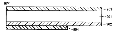
- a photoresist film 904 is formed on a part of the back surface of the a-Si (i / p) layer 902.
- the photoresist film 904 is formed by applying a photoresist to the entire back surface of the a-Si (i / p) layer 902 and then patterning the photoresist by a photolithography technique and an etching technique.
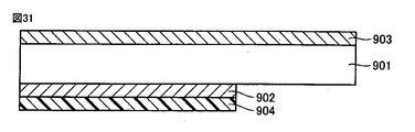
- the back surface of the c-Si (n) substrate 901 is exposed by etching a part of the a-Si (i / p) layer 902 using the photoresist film 904 as a mask. .
- the back surface of the a-Si (i / p) layer 902 exposed by removing the photoresist film 904 and etching are removed.
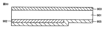
- A-Si (i / n) in which an i-type amorphous silicon film and an n-type amorphous silicon film are laminated in this order so as to cover the back surface of the c-Si (n) substrate 901 exposed by Layer 905 is formed.
- a photoresist film 906 is formed on a part of the back surface of the a-Si (i / n) layer 905.
- the photoresist film 906 is formed by applying a photoresist to the entire back surface of the a-Si (i / n) layer 905 and then patterning the photoresist by a photolithography technique and an etching technique.
- a part of the a-Si (i / n) layer 905 is etched using the photoresist film 906 as a mask, so that the back surface of the a-Si (i / p) layer 902 is removed. Expose.
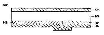
- a transparent conductive oxide film 907 is formed so as to cover the back surface of the a-Si (i / p) layer 902 exposed by the above.
- a photoresist film 908 is formed on a part of the back surface of the transparent conductive oxide film 907.
- the photoresist film 908 is formed by applying a photoresist to the entire back surface of the transparent conductive oxide film 907 and then patterning the photoresist by a photolithography technique and an etching technique.
- a part of the transparent conductive oxide film 907 is etched using the photoresist film 908 as a mask, so that the a-Si (i / p) layer 902 and the a-Si (i / n) ) Expose the back side of the layer 905.
- the photoresist film 908 is removed, the a-Si (i / p) layer 902 and the a-Si (i / n) layer 905 are exposed as shown in FIG.
- a photoresist film 909 is formed so as to cover the back surface and a part of the back surface of the transparent conductive oxide film 907.
- the photoresist film 909 is formed by applying a photoresist to the entire exposed back surface of the a-Si (i / p) layer 902 and the a-Si (i / n) layer 905 and the back surface of the transparent conductive oxide film 907. Later, it is formed by patterning a photoresist by photolithography and etching techniques.
- a back electrode layer 910 is formed on the entire back surface of the transparent conductive oxide film 907 and the photoresist film 909. Next, as shown in FIG.
- the back electrode layer 910 is left only on a part of the surface of the transparent conductive oxide film 907, and the photoresist film 909 and the back electrode layer 910 are removed by lift-off.
- an antireflection film 911 is formed on the surface of the a-Si (i / n) layer 903.
- This invention is made
- the place made into the objective is to provide the photoelectric conversion element which can be manufactured with a simple manufacturing process while improving electric power generation efficiency. .
- the photoelectric conversion element of the present invention includes both a p-type and an n-type semiconductor film on the back surface of a semiconductor substrate, and an intermetallic compound layer is formed on the semiconductor film.
- the intermetallic compound layer formed on the p-type semiconductor film and the intermetallic compound layer formed on the n-type semiconductor film are separated by a space.
- the photoelectric conversion element of the present invention includes a first conductivity type semiconductor substrate, a first conductivity type first semiconductor film provided on one surface of the semiconductor substrate, and the first conductivity type on the surface.
- a second semiconductor film of a second conductivity type provided independently of the semiconductor film, and between the semiconductor substrate and the first semiconductor film and / or between the semiconductor substrate and the second semiconductor film.
- a dielectric film provided therebetween, and an intermetallic compound layer is formed on the first semiconductor film and the second semiconductor film.
- a groove is provided on the surface of the semiconductor substrate, and the second semiconductor film is provided on the bottom surface of the groove.
- the side wall of the groove is covered with an insulating film.
- the first semiconductor film and the second semiconductor film are provided apart from each other on one surface of the semiconductor substrate, and the first semiconductor film and the second semiconductor film are separated from each other.
- An insulating film may be provided therebetween.
- the intermetallic compound layer is preferably a metal silicide layer and / or a metal germanide layer.
- the metal silicide layer is preferably a compound layer made of silicon and at least one metal selected from the group consisting of nickel, cobalt and titanium, and the metal germanide is made of nickel, cobalt and titanium.
- a compound layer composed of at least one metal selected from the group and germanium is preferable.
- the insulating film is preferably a thermally oxidized silicon film and / or a silicon nitride film.
- the silicon nitride film is formed by a plasma CVD method. Is preferred.
- the present invention also relates to a method of manufacturing the photoelectric conversion element, wherein the manufacturing method includes the first conductive type first semiconductor film exposed on one surface of the first conductive type semiconductor substrate and the first conductive film.
- the step of forming the intermetallic compound layer is a step of forming a metal silicide layer, and preferably further includes a step of removing the unreacted metal layer after the step of forming the metal silicide layer.
- the step of forming the intermetallic compound layer is a step of forming a metal germanide layer, and may further include a step of removing the unreacted metal layer after the step of forming the metal germanide layer.
- the metal layer is preferably a layer made of at least one metal selected from the group consisting of nickel, cobalt and titanium.
- the first conductivity type indicates n-type or p-type
- the second conductivity type indicates p-type or n-type different from the first conductivity type
- FIG. 1 shows a schematic cross-sectional view of a photoelectric conversion element 1 according to the first embodiment of the present invention.
- the photoelectric conversion element 1 according to the first embodiment has a semiconductor substrate 3 made of n-type single crystal silicon, and a part of the back surface, which is one surface of the semiconductor substrate 3, includes a bottom surface 11a and its bottom surface.
- a groove 11 having side walls 11b on both sides is provided.
- channel 11 is extended
- a first dielectric film 7 made of i-type amorphous silicon is provided on a region other than the groove on the back surface of the semiconductor substrate 3, and the n-type amorphous silicon is made on the first dielectric film 7.
- a first semiconductor film 8 is provided.
- An intermetallic compound layer 15 is formed on the entire back surface of the first semiconductor film 8.
- the “semiconductor film” refers to a film made of a material that can impart conductivity by doping impurities.
- Examples of such a semiconductor film include a silicon film, a germanium film, and a gallium arsenide film.
- i-type means that n-type or p-type impurities are not intentionally doped.
- n-type or p-type impurities are unavoidable after the photoelectric conversion element is manufactured.
- the n-type or p-type conductivity may be exhibited by diffusion or the like.
- amorphous silicon includes those in which dangling bonds of silicon atoms such as hydrogenated amorphous silicon are terminated with hydrogen.
- amorphous germanium includes hydrogenated amorphous germanium and the like.
- a second dielectric film 12 made of i-type amorphous silicon is provided on the bottom surface 11 a of the groove 11 on the back surface of the semiconductor substrate 3, and p-type amorphous silicon is formed on the second dielectric film 12.
- a second semiconductor film 13 made of is provided.
- An intermetallic compound layer 15 is formed on the entire back surface of the second semiconductor film 13.
- An insulating film 16 may be provided on at least a part of the side wall 11 b of the groove 11. In this case, since the insulating film 16 is provided between the second dielectric film 12 and the second semiconductor film 13 and the sidewall 11b of the groove 11, the second dielectric film 12 and the second semiconductor The film 13 is not in contact with the side wall 11b.
- a third dielectric film 4 made of i-type amorphous silicon is provided on the entire surface of the light-receiving surface (the surface opposite to the back surface) which is the other surface of the semiconductor substrate 3.
- a third semiconductor film 5 made of n-type amorphous silicon is provided on the entire surface of the dielectric film 4. Further, an antireflection film 6 is provided on the entire surface of the third semiconductor film 5.
- the first dielectric film 7 is provided between the back surface of the semiconductor substrate 3 and the back surface of the first semiconductor film 8, and the bottom surface 11a of the groove 11 and A second dielectric film 12 is provided between the back surface of the second semiconductor film 13.
- the intermetallic compound layer 15 is provided on the entire back surface of the first semiconductor film 8 and the entire back surface of the second semiconductor film 13, the first semiconductor film 8. All of the second semiconductor film 13 is covered with the intermetallic compound layer 15.
- the first semiconductor film 8 is n-type and the second semiconductor film 13 is p-type, but the first semiconductor film is p-type, Even if the second semiconductor film is n-type, the effect of the present invention is exhibited.
- the third semiconductor film 5 is not necessarily an essential element, and the third semiconductor film 5 is provided. Even if it is a structure which is not, the effect of this invention shall be shown.
- ⁇ Semiconductor substrate As the semiconductor substrate 3, a substrate typically made of n-type single crystal silicon can be used. However, the material is not limited to this, and conventionally known materials can be widely used. For example, a substrate made of germanium or a gallium arsenide compound may be used, and not only a single crystal substrate but also a polycrystalline substrate or an amorphous substrate may be used. Further, for example, a semiconductor substrate in which a texture structure (not shown) is previously formed on the light receiving surface and / or the back surface of the semiconductor substrate 3 may be used.
- the thickness of the semiconductor substrate 3 is preferably 50 ⁇ m or more and 300 ⁇ m or less. When the thickness of the semiconductor substrate 3 is within the above range, recombination of electron / hole pairs generated in the semiconductor substrate 3 can be prevented and power loss can be reduced.
- a more preferable range of the thickness of the semiconductor substrate 3 is 100 ⁇ m or more and 200 ⁇ m or less.
- the impurity concentration of the semiconductor substrate 3 is not particularly limited, but may be, for example, 5 ⁇ 10 14 pieces / cm 3 or more and 2 ⁇ 10 16 pieces / cm 3 or less.
- phosphorus, boron, or the like can be used as the impurity contained in the semiconductor substrate 3.
- the depth D of the groove 11 is not particularly limited, but may be, for example, 10 ⁇ m or less, and preferably 5 ⁇ m or less.
- the insulating film 16 is not particularly limited as long as it has a resistivity of 1 ⁇ 10 4 ⁇ ⁇ cm or more, and a conventionally known insulating film can be used.
- a silicon oxide film, a silicon nitride film, an aluminum nitride film, an aluminum oxide film, a titanium oxide film, or a combination thereof can be given.
- a silicon oxide film formed by thermal oxidation (also referred to as a thermal silicon oxide film in this specification) is particularly suitable. Since the thermally oxidized silicon film is formed at a high temperature of about 1000 ° C., it exhibits a good passivation effect without changing its properties even at a high temperature of about 250 ° C. in the manufacturing process of the solar cell. More preferably, it is preferable that a thermal annealing process is performed on the thermally oxidized silicon film in addition to the thermally oxidized process. By the hydrogen annealing treatment, dangling bonds at the interface between the semiconductor substrate 3 and the thermally oxidized silicon film can be terminated with hydrogen.
- the insulating film 16 is a silicon nitride film formed by a plasma CVD (Chemical Vapor Deposition) method.
- a plasma CVD Chemical Vapor Deposition
- a mixed gas composed of silane gas (SiH 4 ) and ammonia gas (NH 3 ) is used as a source gas, and the insulating film after hydrogen from the source gas is formed It remains in.
- the presence of hydrogen remaining in the insulating film as described above is generally not preferable from the viewpoint of impurities.
- the present inventors have a function in which when hydrogen in amorphous silicon is desorbed due to photodegradation or the like, hydrogen remaining in the insulating film compensates for this hydrogen defect. Newly found to have. Therefore, the lifetime of the photoelectric conversion element can be extended by containing hydrogen in the insulating film.
- the hydrogen content in the insulating film is preferably 0.005 at% or more and 0.03 at% or less. Exceeding 0.03 at% is not preferable because hydrogen is easily released in the solar cell manufacturing process after the formation of the insulating film, and the insulating film is likely to be distorted or peeled off. Further, if it is less than 0.005 at%, the above effects may not be sufficiently obtained, which is not preferable.
- the hydrogen content can be estimated by integrating signals derived from N—H or Si—H, for example, by the FT-IR method.
- “at%” indicates “atomic percentage”, that is, the atomic number concentration.
- the insulating film 16 may be a single layer film or a laminated film. That is, the insulating film of the present invention is preferably a thermally oxidized silicon film and / or a silicon nitride film.
- the insulating film 16 preferably covers at least a part of the side wall 11b of the groove 11, and more preferably the length of contact between the insulating film 16 and the side wall 11b of the groove 11 is the second dielectric film 12 and the second dielectric film 12. It is longer than the total thickness of the semiconductor film 13, and most preferably, the insulating film 16 covers the entire side wall 11 b of the trench 11.
- the length of the portion in contact with the bottom surface 11 a of the groove 11 is preferably 1 nm or more and 500 nm or less in any vertical cross section with respect to the surface of the semiconductor substrate 3.
- the length is less than 1 nm, the effect of electrically separating the p-type electrode and the n-type electrode may not be sufficiently obtained.
- the length exceeds 500 nm, inconvenience such as peeling during etching occurs. Is not preferable.
- the first semiconductor film, the second semiconductor film, and the third semiconductor film are preferably amorphous films, and typically, amorphous silicon exhibiting p-type or n-type conductivity. And / or a film made of amorphous germanium.
- the first semiconductor film 8 is not limited to a film made of n-type amorphous silicon.
- a conventionally known n-type amorphous semiconductor film may be used.
- a film made of n-type amorphous germanium may be included.
- the thickness of the 1st semiconductor film 8 is not specifically limited, For example, they are 1 nm or more and 20 nm or less.
- the n-type impurity contained in the first semiconductor film 8 for example, phosphorus can be used, and the n-type impurity concentration of the first semiconductor film 8 is, for example, about 5 ⁇ 10 19 / cm 3. can do.
- the second semiconductor film 13 is not limited to a film made of p-type amorphous silicon.
- a conventionally known p-type amorphous semiconductor film may be used.
- a film made of p-type amorphous germanium may be included.
- the thickness of the second semiconductor film 13 is not particularly limited, but may be, for example, 1 nm or more and 20 nm or less.
- the p-type impurity contained in the second semiconductor film 13 for example, boron can be used.
- the p-type impurity concentration of the second semiconductor film 13 is, for example, about 5 ⁇ 10 19 / cm 3. can do.
- the third semiconductor film 5 is not particularly limited as long as it is a translucent film.
- a conventionally known n-type amorphous semiconductor film may be used.
- the thickness of the 3rd semiconductor film 5 is not specifically limited, For example, it is 1 nm or more and 20 nm or less.
- the n-type impurity contained in the third semiconductor film 5 for example, phosphorus can be used, and the n-type impurity concentration of the third semiconductor film 5 is, for example, about 5 ⁇ 10 19 / cm 3. it can.
- the dielectric film is formed between the semiconductor substrate and each semiconductor film, and does not hinder electrical conduction between the semiconductor substrate and each semiconductor film, and passivates the interface between the semiconductor substrate and each semiconductor film. It is a membrane.
- a dielectric film an i-type non-doped film is preferable.
- a film made of i-type amorphous silicon or the like can be suitably used.
- each dielectric film will be described.
- the first dielectric film 7 is formed between the semiconductor substrate 3 and the first semiconductor film 8.
- the first dielectric film 7 is not limited to a film made of i-type amorphous silicon.
- a conventionally known i-type amorphous semiconductor film may be used.
- the thickness of the 1st dielectric film 7 is not specifically limited, For example, they are 1 nm or more and 20 nm or less.
- the second dielectric film 12 is formed between the semiconductor substrate 3 and the second semiconductor film 13.
- the second dielectric film 12 is not limited to a film made of i-type amorphous silicon.
- a conventionally known i-type amorphous semiconductor film may be used.
- the thickness of the second dielectric film 12 is not particularly limited, but may be, for example, 1 nm or more and 20 nm or less.
- the third dielectric film 4 is formed between the semiconductor substrate 3 and the third semiconductor film 5.
- the third dielectric film 4 is not limited to a film made of i-type amorphous silicon.
- a conventionally known i-type amorphous semiconductor film may be used.
- the thickness of the 3rd dielectric film 4 is not specifically limited, For example, they are 1 nm or more and 20 nm or less.
- the intermetallic compound layer 15 of the present invention functions as a p-type electrode or an n-type electrode.
- the intermetallic compound layer 15 is preferably one that exhibits metallic electrical conductivity, and more preferably a metal silicide layer and / or a metal germanide layer.
- the metal silicide for example, nickel silicide (NiSi), cobalt silicide (CoSi 2 ), titanium silicide (TiSi 2 ), molybdenum silicide (MoSi 2 ), palladium silicide (PdSi), platinum silicide (PtSi), manganese Examples thereof include silicide (MnSi 1.7 ), tungsten silicide (WSi 2 ), and the like. Of these, nickel silicide, cobalt silicide, titanium silicide, and combinations thereof can be suitably used. That is, the metal silicide layer of the present invention is preferably a compound layer made of silicon and at least one metal selected from the group consisting of nickel (Ni), cobalt (Co), and titanium (Ti).
- the metal germanide examples include nickel germanide (NiGe, NiGe 2 ), cobalt germanide (CoGe 2 ), titanium germanide (TiGe 2 ), molybdenum germanide (MoGe 2 ), and palladium germana. Id, platinum germanide (PtGe), manganese germanide (Mn 5 Ge 3 ), tungsten germanide (WGe 2 ) and the like. Of these, nickel germanide, cobalt germanide, titanium germanide, and combinations thereof can be suitably used. That is, the metal germanide layer of the present invention is preferably a compound layer made of germanium and at least one metal selected from the group consisting of nickel (Ni), cobalt (Co) and titanium (Ti).
- the intermetallic compound of the present invention may be a compound obtained by doping the above compound with a small amount of other elements.
- each atomic ratio follows the above general formula.
- the compound when the compound is represented by the chemical formula as described above, it is assumed that all the conventionally known atomic ratios are included unless the atomic ratio is particularly limited, and are not necessarily limited to those in the stoichiometric range. .
- the atomic ratio between “Ni” and “Si” is not limited to 50:50, and any conventionally known atomic ratio is included.
- intermetallic compound layer 15 may be a single layer or may be laminated. Further, a silicon germanide layer may be included.
- the thickness of the intermetallic compound layer 15 can be 0.1 ⁇ m or more and 1.0 ⁇ m or less, and more preferably 0.5 ⁇ m or more and 0.8 ⁇ m or less.
- the antireflection film 6 for example, a silicon oxide film, a silicon nitride film, or the like can be used, and the thickness of the antireflection film 6 can be set to, for example, not less than 10 nm and not more than 200 nm. If the thickness of the antireflection film 6 is less than 10 nm, the effect as an antireflection film may not be sufficiently obtained, and if it exceeds 200 nm, sunlight is not easily transmitted, which is not preferable.
- Such a photoelectric conversion element of this embodiment is manufactured by the following manufacturing method.
- the photoelectric conversion element manufactured by the following manufacturing method exhibits the above characteristics. Therefore, the photoelectric conversion element of this Embodiment is a photoelectric conversion element which can be manufactured with a simple manufacturing process while improving electric power generation efficiency.
- an alkali-resistant resist film 9 having an opening 10 is formed on the opposite side (that is, the back surface) of the light receiving surface of the semiconductor substrate 3 made of n-type single crystal silicon.
- the resist film 9 is not particularly limited, but, for example, a resist film 9 formed by printing an alkali-resistant resist ink at a place other than the place where the opening 10 is formed by an ink jet method and drying it is used. be able to.
- a groove 11 comprising a side wall 11b extending in the vertical direction is formed.
- an insulating film 16 is formed on the entire back surface of the semiconductor substrate 3 including the bottom surface 11a and the side wall 11b of the groove 11 as shown in FIG.
- the method for forming the insulating film 16 is not particularly limited, and any conventionally known method can be employed.
- the insulating film 16 When the insulating film 16 is a silicon oxide film, it can be formed by steam oxidation, atmospheric pressure CVD, or the like, but is preferably formed by thermal oxidation.
- the treatment temperature by the thermal oxidation method is preferably 800 ° C. to 1100 ° C.
- Film formation by thermal oxidation is a simple method, and is preferable in comparison with other manufacturing methods because the formed silicon oxide film has good properties, is dense, and has a passivation effect.
- the thickness of the insulating film 16 to be formed can be adjusted depending on the processing time, and can be, for example, 1 nm to 500 nm.
- a hydrogen annealing process may be performed after the thermal oxidation process.
- the treatment temperature of the hydrogen annealing treatment can be set to 300 ° C. to 500 ° C., for example.
- the insulating film 16 when it is a silicon nitride film, it can be formed by a vapor deposition method or the like, but is preferably formed by a plasma CVD method.
- a silicon nitride film is formed by a plasma CVD method, a mixed gas composed of silane (SiH 4 ) gas and ammonia (NH 3 ) gas can be used as a source gas.
- the thickness of the insulating film 16 to be formed can be adjusted by the film forming time, the film forming pressure, etc., and can be, for example, 1 nm to 500 nm.
- the insulating film 16 formed on the flat portion on the back surface of the semiconductor substrate 3 is removed.
- the semiconductor substrate 3 in which the insulating film 16 is formed on the side wall 11b of the groove 11 can be obtained.
- the method for removing the insulating film 16 is not particularly limited, and either dry etching or wet etching may be used.
- the third dielectric film 4 made of i-type amorphous silicon and the first made of n-type amorphous silicon are formed on the entire light-receiving surface of the semiconductor substrate 3 made of n-type single crystal silicon.
- Three semiconductor films 5 are stacked in this order, for example, by a plasma CVD method.
- an antireflection film 6 is laminated on the entire surface of the third semiconductor film 5 by, for example, sputtering, CVD, vapor deposition or the like.
- the second dielectric film 12 made of i-type amorphous silicon and the p-type amorphous silicon are formed on the entire back surface of the semiconductor substrate 3 having the insulating film 16 on the side wall 11b of the groove 11.
- the second semiconductor film 13 to be formed is laminated in this order, for example, by a plasma CVD method.
- the second semiconductor film 13 may be formed by laminating a film made of p-type amorphous silicon and a film made of p-type amorphous germanium, and in that case, a film made of p-type amorphous silicon.
- a film made of p-type amorphous germanium is laminated on the substrate by, for example, a plasma CVD method.
- a mask material 14 is embedded in at least a part of the groove 11.
- the embedding of the groove 11 with the mask material 14 is performed, for example, by heating the mask material 14 to a molten state, and selectively applying the mask material 14 so as to embed the groove 11 by an inkjet method, and cooling to solidify the groove 11. And then drying.
- the mask material 14 is not particularly limited as long as it functions as an etching mask for the second dielectric film 12 and the second semiconductor film 13, but a hot melt adhesive is preferably used.
- the hot melt adhesive is in a solid state at room temperature, but has a characteristic that it becomes a molten state by heating and has less bleeding after coating.
- the second dielectric film 12 and the second semiconductor film 13 not covered with the mask material 14 are removed.
- a method for removing the second dielectric film 12 and the second semiconductor film 13 is not particularly limited, but it is preferable to use dry etching.
- the mask material 14 is removed and then washed.
- the method for removing the mask material 14 is not particularly limited.
- the mask material 14 is made of a hot melt adhesive
- a method of immersing the mask material 14 in warm water and peeling it off can be used.
- the first dielectric film 7 made of i-type amorphous silicon and the n-type amorphous silicon are formed on the entire back surface of the semiconductor substrate 3 after the mask material 14 is removed.
- the first semiconductor film 8 is laminated in this order, for example, by a plasma CVD method.
- the first semiconductor film 8 may be formed by laminating a film made of n-type amorphous silicon and a film made of n-type amorphous germanium, and in that case, a film made of n-type amorphous silicon.
- a film made of n-type amorphous germanium is laminated on the substrate by, for example, a plasma CVD method.
- a resist film 17 is formed in a portion other than the opening 10 on the back surface of the semiconductor substrate 3.
- the resist film 17 is not specifically limited, For example, what was illustrated above can be used.
- the first dielectric film 7 and the first semiconductor film 8 exposed from the opening 10 of the resist film 17 are removed, and the second dielectric film 7 formed in the trench 11 is removed.
- the semiconductor film 13 is exposed.
- wet etching using an alkaline solution it is preferable to use wet etching using an alkaline solution. That is, since the p-type second semiconductor film 13 is difficult to be removed by wet etching using an alkaline solution, the second semiconductor film 13 functions as an etching stop layer, and the first dielectric film 7 and the first 1 semiconductor film 8 can be removed reliably.
- it does not specifically limit as an alkaline solution For example, what was illustrated above can be used.
- a metal layer 20 is formed on the entire back surface of the semiconductor substrate 3.
- the metal layer 20 can be formed by a conventionally known method. For example, a CVD method, a sputtering method, a vapor deposition method, or the like can be suitably used.
- the metal layer 20 is preferably made of at least one metal selected from the group consisting of nickel (Ni), cobalt (Co), and titanium (Ti). It can be 1 ⁇ m or more and 1.0 ⁇ m or less.
- the metal layer 20 after forming the metal layer 20, heat treatment is performed to cause the metal layer 20 to react with the first semiconductor film 8 and the second semiconductor film 13, thereby intermetallic compound.
- Layer 15 can be formed.
- the heat treatment temperature is more preferably 200 ° C. or higher and 600 ° C. or lower.
- the intermetallic compound layer 15 is made of the metal germanide. It can be a layer.
- the heat treatment temperature is preferably 100 ° C. or more and 500 ° C. or less.
- the metal germanide layer is preferable because it can be formed at a lower temperature than the metal silicide layer.
- the reason for this is that when a groove is formed in the semiconductor substrate as in the present embodiment, if the heat treatment is performed at a high temperature exceeding 600 ° C., the groove (that is, the portion where the thickness of the semiconductor substrate is different) is caused. This is because there is a possibility that problems such as warpage may occur in the semiconductor substrate. Therefore, in order to suppress the occurrence of such a problem, the temperature at which the metal layer and the semiconductor film are reacted needs to be 600 ° C. or less.
- the metal germanide layer can be formed at a temperature of 500 ° C. or less, and is particularly suitable because it does not cause problems such as warpage of the semiconductor substrate.
- the unreacted metal layer 20 is removed.
- the intermetallic compound layer 15 on the first semiconductor film 8 and the intermetallic compound layer 15 on the second semiconductor film 13 become the first semiconductor film serving as a base. 8 and the second semiconductor film 13 are separated according to the shape of the semiconductor film 13 (ie, separated in a self-aligned manner). Thereby, the intermetallic compound layer 15 is separated into a p-type electrode and an n-type electrode.
- the present embodiment unlike the solar cell having the structure shown in FIG. 44, it is not necessary to connect the semiconductor film and the electrode layer by the transparent conductive oxide film, so that the contact resistance is reduced, and the photoelectric conversion element Conversion efficiency can be increased.
- the low resistance electrode composed of the intermetallic compound layer is formed as described above, and it is simple and reliable.
- the p-type electrode (electrode on the second semiconductor film 13) and the n-type electrode (electrode on the first semiconductor film 8) can be separated.
- the p-type electrode and the n-type electrode are formed at different positions in the thickness direction of the semiconductor substrate, the gap between the p-type electrode and the n-type electrode on the back surface of the semiconductor substrate. In addition, it is not necessary to perform precise patterning for forming such a p-type electrode and an n-type electrode with a small gap.
- the amorphous film (the first semiconductor film 8 and the second semiconductor film 13) does not flow easily in the horizontal direction (the surface direction of the film), the p-type electrode and the n-type electrode on the back surface of the semiconductor substrate It is preferable from the viewpoint of obtaining a photoelectric conversion element having high conversion efficiency that the gap between them is as small as possible.
- the p-type electrode and the n-type electrode are electrically separated by the groove formed on the back surface and the insulating film formed on the groove side wall. A reduction in conversion efficiency that occurs when separation is insufficient is prevented.
- the semiconductor substrate since the entire back surface of the semiconductor substrate can be covered with the p-type electrode and the n-type electrode, the semiconductor substrate is not absorbed in the light incident from the light receiving surface side of the semiconductor substrate.
- the light that has been transmitted to the back side of the light can be reflected by the p-type electrode and the n-type electrode. Further, the light transmitted through the groove side wall can be reflected by the insulating film formed on the groove side wall.
- the entire back surface of the semiconductor substrate including the bottom surface of the groove of the semiconductor substrate is passivated by the i-type dielectric film, the n-type semiconductor film, and the p-type semiconductor film.
- a part of the bottom surface and the side wall of the groove are passivated by the insulating film. Therefore, good passivation characteristics can be obtained over the entire back surface of the semiconductor substrate, and carrier recombination on the surface of the semiconductor substrate can be suppressed.
- a photoelectric conversion element having higher conversion efficiency than that of the solar cell having the structure shown in FIG. 44 can be obtained.
- the photoelectric conversion element which has high conversion efficiency can be manufactured with a simple manufacturing process.
- FIG. 2 shows a schematic cross-sectional view of a photoelectric conversion element 2 according to the second embodiment of the present invention.
- the photoelectric conversion element 2 does not have a groove on the back surface of the semiconductor substrate 103, and the first dielectric film 107 and the second dielectric material made of i-type amorphous silicon are formed on the back surface of the semiconductor substrate 103.
- the film 112 is provided apart from the film 112.
- a first semiconductor film 108 made of n-type amorphous silicon is provided on the first dielectric film 107.
- a second semiconductor film 113 made of p-type amorphous silicon is provided on the second dielectric film 112.
- An intermetallic compound layer 115 is provided on the entire back surface of the first semiconductor film 108 and the second semiconductor film 113.
- an insulating film 116 is provided between the first dielectric film 107 and the second dielectric film 112.
- the insulating film 116 is formed in contact with the side surface portion of the first dielectric film 107 and / or the side surface portion of the second dielectric film 112.
- the insulating film 116 may be in contact with the side surface portion of the first semiconductor film 108 and / or the side surface portion of the second semiconductor film 113.
- a third dielectric film 104, a third semiconductor film 105, and an antireflection film 106 are provided on the light receiving surface of the photoelectric conversion element 2 (the surface opposite to the back surface).
- the photoelectric conversion element 2 a configuration in which the first semiconductor film 108 is n-type and the second semiconductor film 113 is p-type is exemplified, but the first semiconductor film is p-type, Even if the second semiconductor film is n-type, the effect of the present invention is exhibited.
- the third semiconductor film 105 is not necessarily an essential element, and the third semiconductor film 105 is provided. Even if it is a structure which is not, the effect of this invention shall be shown.
- Such a photoelectric conversion element of this embodiment is manufactured by the following manufacturing method.
- the photoelectric conversion element manufactured by the following manufacturing method exhibits the above characteristics. Therefore, the photoelectric conversion element of this Embodiment is a photoelectric conversion element which can be manufactured with a simple manufacturing process while improving electric power generation efficiency.
- a third dielectric film 104 made of i-type amorphous silicon and a third dielectric film made of n-type amorphous silicon are formed on the entire light-receiving surface of a semiconductor substrate 103 made of n-type single crystal silicon.
- the semiconductor film 105 and the antireflection film 106 are stacked in this order, for example, by a plasma CVD method.
- a first dielectric film 107 made of i-type amorphous silicon and a first semiconductor film made of n-type amorphous silicon are formed on the entire back surface of the semiconductor substrate 103.
- the layers are stacked in this order, for example, by plasma CVD.
- the first semiconductor film 108 may be formed by laminating a film made of n-type amorphous silicon and a film made of n-type amorphous germanium, and in that case, a film made of n-type amorphous silicon.
- a film made of n-type amorphous germanium is laminated on the substrate by, for example, a plasma CVD method.
- a resist film 109 having an opening 110 is formed.
- the resist film 109 is not particularly limited, and, for example, those exemplified above as the alkali-resistant resist film can be used.
- a part of the first dielectric film 107 and the first dielectric film 108 not covered with the resist film 109 is removed, and the semiconductor substrate 103 is exposed.
- a method for removing the first dielectric film 107 and the first semiconductor film 108 is not particularly limited, but wet etching using an alkaline solution is preferably used.
- an insulating film 116 is formed on the entire back surface of the first semiconductor film 108 and the entire back surface of the semiconductor substrate 103, as shown in FIG.
- a method of forming the insulating film 116 for example, the method exemplified above can be used.
- the insulating film 116 is preferably a thermally oxidized silicon film or a silicon nitride film.
- the insulating film 116 is left on the side surfaces of the first dielectric film 107 and the first semiconductor film 108.
- a method for removing the insulating film 116 is not particularly limited, and either dry etching or wet etching may be used.
- a second dielectric film made of i-type amorphous silicon is formed on the entire back surface of the first semiconductor film 108, on the entire back surface of the semiconductor substrate 103, and on the remaining portion of the insulating film 116.
- the second semiconductor film 113 made of 112 and p-type amorphous silicon is laminated in this order by, for example, a plasma CVD method.
- the second semiconductor film 113 may be formed by laminating a film made of p-type amorphous silicon and a film made of p-type amorphous germanium, and in that case, a film made of p-type amorphous silicon.
- a film made of p-type amorphous germanium is laminated on the substrate by, for example, a plasma CVD method.
- the second dielectric film 112 and the second semiconductor film 113 formed on the first semiconductor film 108 and the remaining part of the insulating film 116 are removed.
- a method of removing the second dielectric film 112 and the second semiconductor film 113 for example, dry etching or the like can be used as exemplified above.
- a metal layer 120 is formed on the first semiconductor film 108, the second semiconductor film 113, and the remaining portion of the insulating film 116.
- a method of forming the metal layer 120 a sputtering method or the like can be used as exemplified above, and the metal layer 120 is a group consisting of nickel (Ni), cobalt (Co), and titanium (Ti). It is preferable to consist of at least one kind of metal selected.
- heat treatment is performed to react the metal layer 120 with the first semiconductor film 108 and the second semiconductor film 113 to form an intermetallic compound layer 115.
- the metal layer 120 on the insulating film 116 remains unreacted.
- the intermetallic compound layer 115 is separated into a p-type electrode and an n-type electrode in a self-aligned manner.
- the present embodiment unlike the solar cell having the structure shown in FIG. 44, it is not necessary to connect the semiconductor film and the electrode layer by the transparent conductive oxide film, so that the contact resistance is reduced and the conversion of the photoelectric conversion element is performed. Efficiency can be increased.
- the present embodiment unlike the method shown in FIGS. 37 to 44, it is not necessary to perform a complicated patterning process in forming the electrode, and the low resistance electrode formed of the intermetallic compound layer is formed as described above.
- the p-type electrode (electrode on the second semiconductor film 113) and the n-type electrode (electrode on the first semiconductor film 107) can be separated easily and reliably.
- the entire back surface of the semiconductor substrate is passivated by an i-type dielectric film, an n-type semiconductor film, a p-type semiconductor film, and an insulating film, so that the entire back surface of the semiconductor substrate is ,
- Favorable passivation characteristics can be obtained, and carrier recombination on the surface of the semiconductor substrate can be suppressed.
- a photoelectric conversion element having higher conversion efficiency than that of the solar cell having the structure shown in FIG. 44 can be obtained.
- the photoelectric conversion element which has high conversion efficiency can be manufactured with a simple manufacturing process.
- the present invention can be used in a photoelectric conversion element and a method for manufacturing a photoelectric conversion element.
Landscapes
- Photovoltaic Devices (AREA)
- Life Sciences & Earth Sciences (AREA)
- Engineering & Computer Science (AREA)
- Sustainable Development (AREA)
- Sustainable Energy (AREA)
Abstract
第1導電型の半導体基板と、該半導体基板の一方の表面上に設けられた第1導電型の第1の半導体膜と、該表面上に該第1の半導体膜から独立して設けられた第2導電型の第2の半導体膜と、該半導体基板と該第1の半導体膜との間および/または該半導体基板と該第2の半導体膜との間に設けられた誘電体膜と、を備え、該第1の半導体膜上および該第2の半導体膜上に金属間化合物層が形成されている光電変換素子が提供される。
Description
本発明は光電変換素子および光電変換素子の製造方法に関する。
太陽光エネルギを電気エネルギに直接変換する太陽電池は、近年、特に、地球環境問題の観点から、次世代のエネルギ源としての期待が急激に高まっている。太陽電池には、化合物半導体または有機材料を用いたものなど様々な種類のものがあるが、現在、主流となっているのは、シリコン結晶を用いたものである。
現在、最も多く製造および販売されている太陽電池は、太陽光が入射する側の面である受光面と、受光面の反対側である裏面とにそれぞれ電極が形成された構造のものである。
しかしながら、受光面に電極を形成した場合、電極における太陽光の反射および吸収によって、電極の面積分だけ入射する太陽光の量が減少してしまう。そこで、たとえば、特開2010-80887号公報(特許文献1)に示されるような裏面のみに電極が形成された太陽電池の開発が進められている。
以下、図28~図44の模式的断面図を参照して、裏面のみに電極が形成された太陽電池の製造方法の一例について説明する。まず、図28に示すように、受光面にテクスチャ構造(図示せず)が形成されたn型の単結晶シリコンからなるc-Si(n)基板901の裏面上に、i型の非晶質シリコン膜とp型の非晶質シリコン膜とがこの順序に積層されたa-Si(i/p)層902を形成する。
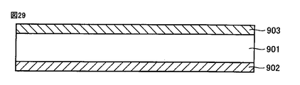
次に、図29に示すように、c-Si(n)基板901の受光面上に、i型の非晶質シリコン膜とn型の非晶質シリコン膜とがこの順序に積層されたa-Si(i/n)層903を形成する。
次に、図30に示すように、a-Si(i/p)層902の一部の裏面上にフォトレジスト膜904を形成する。ここで、フォトレジスト膜904は、a-Si(i/p)層902の裏面の全面にフォトレジストを塗布した後に、フォトリソグラフィー技術およびエッチング技術によってフォトレジストをパターンニングすることによって形成される。
次に、図31に示すように、フォトレジスト膜904をマスクとして、a-Si(i/p)層902の一部をエッチングすることによって、c-Si(n)基板901の裏面を露出させる。
次に、図32に示すように、フォトレジスト膜904を除去した後に、図33に示すように、フォトレジスト膜904を除去して露出したa-Si(i/p)層902の裏面およびエッチングにより露出したc-Si(n)基板901の裏面を覆うようにi型の非晶質シリコン膜とn型の非晶質シリコン膜とがこの順序に積層されたa-Si(i/n)層905を形成する。
次に、図34に示すように、a-Si(i/n)層905の一部の裏面上にフォトレジスト膜906を形成する。ここで、フォトレジスト膜906は、a-Si(i/n)層905の裏面の全面にフォトレジストを塗布した後に、フォトリソグラフィー技術およびエッチング技術によってフォトレジストをパターンニングすることによって形成される。
次に、図35に示すように、フォトレジスト膜906をマスクとして、a-Si(i/n)層905の一部をエッチングすることによって、a-Si(i/p)層902の裏面を露出させる。
次に、図36に示すように、フォトレジスト膜906を除去した後に、図37に示すように、フォトレジスト膜906を除去して露出したa-Si(i/n)層905の裏面およびエッチングにより露出したa-Si(i/p)層902の裏面を覆うように透明導電酸化膜907を形成する。
次に、図38に示すように、透明導電酸化膜907の一部の裏面上にフォトレジスト膜908を形成する。ここで、フォトレジスト膜908は、透明導電酸化膜907の裏面の全面にフォトレジストを塗布した後に、フォトリソグラフィー技術およびエッチング技術によってフォトレジストをパターンニングすることによって形成される。
次に、図39に示すように、フォトレジスト膜908をマスクとして、透明導電酸化膜907の一部をエッチングすることによって、a-Si(i/p)層902およびa-Si(i/n)層905の裏面を露出させる。
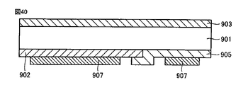
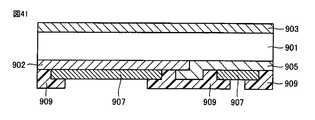
次に、図40に示すように、フォトレジスト膜908を除去した後に、図41に示すように、a-Si(i/p)層902およびa-Si(i/n)層905の露出した裏面および透明導電酸化膜907の一部の裏面を覆うようにフォトレジスト膜909を形成する。ここで、フォトレジスト膜909は、a-Si(i/p)層902およびa-Si(i/n)層905の露出した裏面および透明導電酸化膜907の裏面の全面にフォトレジストを塗布した後に、フォトリソグラフィー技術およびエッチング技術によってフォトレジストをパターンニングすることによって形成される。
次に、図42に示すように、透明導電酸化膜907およびフォトレジスト膜909の裏面全面に裏面電極層910を形成する。
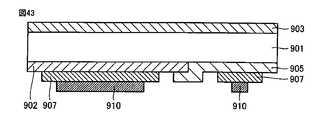
次に、図43に示すように、透明導電酸化膜907の表面の一部のみに裏面電極層910を残すようにして、リフトオフによりフォトレジスト膜909および裏面電極層910を除去する。
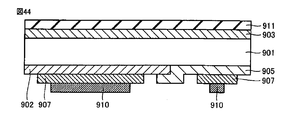
次に、図44に示すように、a-Si(i/n)層903の表面上に反射防止膜911を形成する。
しかしながら、上記の太陽電池の製造方法においては、フォトレジストの塗布、ならびにフォトリソグラフィー技術およびエッチング技術によるフォトレジストの複雑なパターンニング工程を行なう必要があり、裏面のみに電極が形成された太陽電池の製造工程が非常に煩雑であるという問題があった。また、裏面のみに電極が形成された太陽電池の変換効率の向上も要望されている。
本発明は上記のような現状に鑑みなされたものであって、その目的とするところは、発電効率を向上させるとともに、簡易な製造工程で製造することができる光電変換素子を提供することにある。
本発明の光電変換素子は、半導体基板の裏面にp型およびn型の双方の半導体膜を備え、該半導体膜の上には金属間化合物層が形成されている。そして、p型半導体膜の上に形成された金属間化合物層とn型半導体膜の上に形成された金属間化合物層とは空間によって隔離されている。
すなわち、本発明の光電変換素子は、第1導電型の半導体基板と、該半導体基板の一方の表面上に設けられた第1導電型の第1の半導体膜と、該表面上に該第1の半導体膜から独立して設けられた第2導電型の第2の半導体膜と、該半導体基板と該第1の半導体膜との間および/または該半導体基板と該第2の半導体膜との間に設けられた誘電体膜と、を備え、該第1の半導体膜上および該第2の半導体膜上に金属間化合物層が形成されていることを特徴とする。
ここで、上記半導体基板の上記表面には溝が設けられており、該溝の底面に上記第2の半導体膜が設けられていることが好ましい。
さらに、上記溝の側壁の少なくとも一部が絶縁膜で覆われていることが好適である。
また、上記半導体基板の一方の表面上において、上記第1の半導体膜と上記第2の半導体膜とは離間して設けられており、該第1の半導体膜と該第2の半導体膜との間に絶縁膜が設けられていても良い。
また、上記半導体基板の一方の表面上において、上記第1の半導体膜と上記第2の半導体膜とは離間して設けられており、該第1の半導体膜と該第2の半導体膜との間に絶縁膜が設けられていても良い。
また、上記金属間化合物層は、金属シリサイド層および/または金属ジャーマナイド層であることが好ましい。ここで、該金属シリサイド層は、ニッケル、コバルトおよびチタンからなる群より選ばれた少なくとも1種の金属とシリコンとからなる化合物層であることが好ましく、該金属ジャーマナイドは、ニッケル、コバルトおよびチタンからなる群より選ばれた少なくとも1種の金属とゲルマニウムとからなる化合物層であることが好適である。
また、上記絶縁膜は、熱酸化シリコン膜および/または窒化シリコン膜であることが好ましく、該絶縁膜が窒化シリコン膜である場合には、該窒化シリコン膜は、プラズマCVD法によって形成されていることが好適である。
また、本発明は、上記の光電変換素子の製造方法にも係わり、該製造方法は、第1導電型の半導体基板の一方の表面上に露出した第1導電型の第1の半導体膜と第2導電型の第2の半導体膜とを含む該表面側の全面に金属層を形成する工程と、熱処理によって該第1の半導体膜および該第2の半導体膜と該金属層とを反応させて金属間化合物層を形成する工程と、を含むことを特徴とする。
ここで、上記金属間化合物層を形成する工程は、金属シリサイド層を形成する工程であり、該金属シリサイド層を形成する工程の後に未反応の金属層を除去する工程をさらに含むことが好ましい。
また、上記金属間化合物層を形成する工程は、金属ジャーマナイド層を形成する工程であり、該金属ジャーマナイド層を形成する工程の後に未反応の金属層を除去する工程をさらに含んでいても良い。
さらに、上記金属層は、ニッケル、コバルトおよびチタンからなる群より選ばれた少なくとも1種の金属からなる層であることが好ましい。
なお、本明細書において、第1導電型とはn型またはp型であることを示し、第2導電型とは第1導電型とは異なるp型またはn型であることを示す。
本発明によれば、発電効率を向上させるとともに、簡易な製造工程で製造することができる光電変換素子を提供することができる。
以下、本発明の実施の形態について説明する。なお、本発明の図面において、同一の参照符号は、同一部分または相当部分を表わすものとする。
<実施の形態1>
[光電変換素子]
≪全体構成≫
図1に、本発明の第1の実施の形態である光電変換素子1の模式的な断面図を示す。第1の実施の形態である光電変換素子1は、n型単結晶シリコンからなる半導体基板3を有しており、半導体基板3の一方の面である裏面の一部には、底面11aとその両側の側壁11bとを備えた溝11が設けられている。ここで、溝11は、図1の紙面の法線方向に伸長している。
[光電変換素子]
≪全体構成≫
図1に、本発明の第1の実施の形態である光電変換素子1の模式的な断面図を示す。第1の実施の形態である光電変換素子1は、n型単結晶シリコンからなる半導体基板3を有しており、半導体基板3の一方の面である裏面の一部には、底面11aとその両側の側壁11bとを備えた溝11が設けられている。ここで、溝11は、図1の紙面の法線方向に伸長している。
半導体基板3の裏面の溝以外の領域上には、i型のアモルファスシリコンからなる第1の誘電体膜7が設けられており、第1の誘電体膜7上にはn型のアモルファスシリコンからなる第1の半導体膜8が設けられている。そして、第1の半導体膜8の全裏面上には、金属間化合物層15が形成されている。
ここで、本明細書において、「半導体膜」とは、不純物をドープすることによって導電性を付与することができる材料からなる膜を示す。このような半導体膜としては、たとえば、シリコン膜、ゲルマニウム膜、ガリウム砒素膜などを挙げることができる。
また、「i型」とは、n型またはp型の不純物を意図的にドーピングしていないことを意味しており、たとえば、光電変換素子の作製後にn型またはp型の不純物が不可避的に拡散することなどによってn型またはp型の導電型を示すこともあり得る。
また、「アモルファスシリコン」には、水素化アモルファスシリコンなどのシリコン原子の未結合手(ダングリングボンド)が水素で終端されたものも含まれるものとする。同様に、「アモルファスゲルマニウム」には、水素化アモルファスゲルマニウムなどが含まれるものとする。
半導体基板3の裏面の溝11の底面11a上には、i型のアモルファスシリコンからなる第2の誘電体膜12が設けられており、第2の誘電体膜12上にはp型のアモルファスシリコンからなる第2の半導体膜13が設けられている。そして、第2の半導体膜13の全裏面上には金属間化合物層15が形成されている。
溝11の側壁11bの少なくとも一部には、絶縁膜16が設けられていても良い。この場合、第2の誘電体膜12および第2の半導体膜13と溝11の側壁11bとの間には絶縁膜16が設けられているため、第2の誘電体膜12および第2の半導体膜13は側壁11bとは接していない。
また、半導体基板3の他方の面である受光面(裏面の反対側の面)の全面上には、i型のアモルファスシリコンからなる第3の誘電体膜4が設けられており、第3の誘電体膜4の全面上にはn型のアモルファスシリコンからなる第3の半導体膜5が設けられている。さらに、第3の半導体膜5の全面上には反射防止膜6が設けられている。
以上の構造を有する光電変換素子1においては、半導体基板3の裏面と第1の半導体膜8の裏面との間には第1の誘電体膜7が設けられており、溝11の底面11aと第2の半導体膜13の裏面との間には第2の誘電体膜12が設けられている。
したがって、光電変換素子1においては、半導体基板3の裏面と第1の半導体膜8の裏面との間、および溝11の底面11aと第2の半導体膜13の裏面との間のすべての領域に誘電体膜が設けられている。
また、光電変換素子1においては、第1の半導体膜8の全裏面上および第2の半導体膜13の全裏面上に金属間化合物層15が設けられていることから、第1の半導体膜8および第2の半導体膜13のすべてが金属間化合物層15によって覆われている。
なお、光電変換素子1においては、第1の半導体膜8がn型であり、かつ第2の半導体膜13がp型である構成を例示するが、第1の半導体膜がp型であり、かつ第2の半導体膜がn型であっても本発明の効果は示される。
また、光電変換素子1においては、受光面に第3の半導体膜5が設けられた構成を例示するが、第3の半導体膜5は必ずしも必須の要素ではなく、第3の半導体膜5を有しない構成であったとしても、本発明の効果は示されるものとする。
以下、本実施の形態の光電変換素子を構成する各要素について説明する。
≪半導体基板≫
半導体基板3としては、典型的にはn型単結晶シリコンからなる基板を用いることができるが、材質はこれに限定されず、従来公知の材質を広く用いることができる。たとえば、ゲルマニウムやガリウム砒素化合物からなる基板を用いても良く、また、単結晶基板のみならず多結晶基板やアモルファス基板を用いても良い。また、たとえば、予め半導体基板3の受光面および/または裏面にテクスチャ構造(図示せず)が形成された半導体基板などであっても良い。
≪半導体基板≫
半導体基板3としては、典型的にはn型単結晶シリコンからなる基板を用いることができるが、材質はこれに限定されず、従来公知の材質を広く用いることができる。たとえば、ゲルマニウムやガリウム砒素化合物からなる基板を用いても良く、また、単結晶基板のみならず多結晶基板やアモルファス基板を用いても良い。また、たとえば、予め半導体基板3の受光面および/または裏面にテクスチャ構造(図示せず)が形成された半導体基板などであっても良い。
半導体基板3の厚さは、50μm以上300μm以下であることが好ましい。半導体基板3の厚さが該範囲内であることにより、半導体基板3内で生成された電子・正孔ペアの再結合を防止し電力損失を低減することができる。ここで、半導体基板3の厚さとして、より好ましい範囲は、100μm以上200μm以下である。
また、半導体基板3の不純物濃度も特に限定されないが、たとえば5×10¹⁴個/cm3以上2×1016個/cm3以下とすることができる。半導体基板3に含まれる不純物としては、たとえば、リン、ボロンなどを用いることができる。
≪溝≫
また、溝11の深さDは、特に限定されないが、たとえば10μm以下とすることができ、好ましくは5μm以下とすることができる。
また、溝11の深さDは、特に限定されないが、たとえば10μm以下とすることができ、好ましくは5μm以下とすることができる。
≪絶縁膜≫
絶縁膜16としては、抵抗率が1×10⁴Ω・cm以上の絶縁性を有する膜であれば特に限定されず、従来公知の絶縁膜を用いることができる。たとえば、酸化シリコン膜、窒化シリコン膜、窒化アルミニウム膜、酸化アルミニウム膜、酸化チタニウム膜またはこれらの併用などを挙げることができる。
絶縁膜16としては、抵抗率が1×10⁴Ω・cm以上の絶縁性を有する膜であれば特に限定されず、従来公知の絶縁膜を用いることができる。たとえば、酸化シリコン膜、窒化シリコン膜、窒化アルミニウム膜、酸化アルミニウム膜、酸化チタニウム膜またはこれらの併用などを挙げることができる。
これらのうち、熱酸化によって形成された酸化シリコン膜(本明細書において、熱酸化シリコン膜とも記す)が特に好適である。熱酸化シリコン膜は、1000℃程度の高温で形成されるため、太陽電池の製造工程における250℃程度の高温過程においてもその性質を変化させることなく良好なパッシベーション効果を示す。そして、より好ましくは、熱酸化シリコン膜に、熱酸化処理に加えて水素アニール処理が行なわれていることが好適である。水素アニール処理により、半導体基板3と熱酸化シリコン膜界面のダングリングボンドを水素で終端させることができる。
また、絶縁膜16が、プラズマCVD(Chemical Vapor Deposition)法によって形成された窒化シリコン膜であることも好ましい態様の一つである。プラズマCVD法によって窒化シリコン膜を形成する場合には、原料ガスにシランガス(SiH4)およびアンモニアガス(NH3)などからなる混合ガスが用いられ、該原料ガス由来の水素が形成後の絶縁膜中に残留する。
上記のような絶縁膜中に残留する水素の存在は、不純物の観点から一般的には好ましくない。しかし、本発明者らは、本発明の構成を備えた光電変換素子において、光劣化などにより、アモルファスシリコン中の水素が脱離した場合、絶縁膜中に残留した水素がこの水素欠陥を補う機能を有することを新たに見出した。したがって、絶縁膜中に水素を含有させることで、光電変換素子の長寿命化を図ることができる。
ここで、絶縁膜中の水素含有量は、好ましくは0.005at%以上0.03at%以下である。0.03at%を超過すると、絶縁膜形成後の太陽電池製造過程において、水素が脱離しやすく、絶縁膜に歪みや剥離が生じやすく好ましくない。また、0.005at%未満であると、上記のような効果が十分に得られない場合があり好ましくない。
なお、水素含有量は、たとえばFT-IR法によって、N-HやSi-Hに由来する信号を積分することにより見積もることができる。また、「at%」とは、「atomic percentage」、すなわち原子個数濃度を示す。
また、絶縁膜16は、単層膜であって良く、積層膜であっても良い。すなわち、本発明の絶縁膜は、熱酸化シリコン膜および/または窒化シリコン膜であることが好ましい。
さらに、絶縁膜16は、溝11の側壁11bの少なくとも一部を覆うことが好ましく、より好ましくは絶縁膜16と溝11の側壁11bの接する長さが第2の誘電体膜12および第2の半導体膜13の厚さの総和よりも長く、最も好ましくは絶縁膜16が溝11の側壁11bの全面を覆うことが好適である。また、絶縁膜16は、半導体基板3の表面に対する任意の垂直断面において、溝11の底面11aと接する部分の長さが1nm以上500nm以下であることが好ましい。上記長さが1nm未満であると、p型電極とn型電極とを電気的に分離する効果が十分得られない場合があり、500nmを超過するとエッチングの際に剥離するなどの不都合を生じる場合があり好ましくない。
≪半導体膜≫
本発明において、第1の半導体膜、第2の半導体膜および第3の半導体膜は、非晶質膜であることが好ましく、典型的には、p型またはn型の導電性を示すアモルファスシリコンおよび/またはアモルファスゲルマニウムからなる膜である。以下、各半導体膜について説明する。
本発明において、第1の半導体膜、第2の半導体膜および第3の半導体膜は、非晶質膜であることが好ましく、典型的には、p型またはn型の導電性を示すアモルファスシリコンおよび/またはアモルファスゲルマニウムからなる膜である。以下、各半導体膜について説明する。
(第1の半導体膜)
第1の半導体膜8としてはn型のアモルファスシリコンからなる膜に限定されず、たとえば、従来から公知のn型のアモルファス半導体膜などを用いても良い。また、たとえば、n型のアモルファスゲルマニウムからなる膜を含んでいても良い。第1の半導体膜8の厚さは特に限定されないが、たとえば1nm以上20nm以下とすることができる。ここで、第1の半導体膜8に含まれるn型不純物としては、たとえばリンを用いることができ、第1の半導体膜8のn型不純物濃度は、たとえば5×10¹⁹個/cm3程度とすることができる。
第1の半導体膜8としてはn型のアモルファスシリコンからなる膜に限定されず、たとえば、従来から公知のn型のアモルファス半導体膜などを用いても良い。また、たとえば、n型のアモルファスゲルマニウムからなる膜を含んでいても良い。第1の半導体膜8の厚さは特に限定されないが、たとえば1nm以上20nm以下とすることができる。ここで、第1の半導体膜8に含まれるn型不純物としては、たとえばリンを用いることができ、第1の半導体膜8のn型不純物濃度は、たとえば5×10¹⁹個/cm3程度とすることができる。
(第2の半導体膜)
第2の半導体膜13としてはp型のアモルファスシリコンからなる膜に限定されず、たとえば従来から公知のp型のアモルファス半導体膜などを用いても良い。また、たとえばp型のアモルファスゲルマニウムからなる膜を含んでいても良い。第2の半導体膜13の厚さは、特に限定されないが、たとえば1nm以上20nm以下とすることができる。ここで、第2の半導体膜13に含まれるp型不純物としては、たとえばボロンを用いることができ、第2の半導体膜13のp型不純物濃度は、たとえば5×10¹⁹個/cm3程度とすることができる。
第2の半導体膜13としてはp型のアモルファスシリコンからなる膜に限定されず、たとえば従来から公知のp型のアモルファス半導体膜などを用いても良い。また、たとえばp型のアモルファスゲルマニウムからなる膜を含んでいても良い。第2の半導体膜13の厚さは、特に限定されないが、たとえば1nm以上20nm以下とすることができる。ここで、第2の半導体膜13に含まれるp型不純物としては、たとえばボロンを用いることができ、第2の半導体膜13のp型不純物濃度は、たとえば5×10¹⁹個/cm3程度とすることができる。
(第3の半導体膜)
第3の半導体膜5は、透光性を示す膜であれば特に限定されず、たとえば従来から公知のn型のアモルファス半導体膜などを用いても良い。第3の半導体膜5の厚さは特に限定されないが、たとえば1nm以上20nm以下とすることができる。第3の半導体膜5に含まれるn型不純物としては、たとえばリンを用いることができ、第3の半導体膜5のn型不純物濃度は、たとえば5×10¹⁹個/cm3程度とすることができる。
第3の半導体膜5は、透光性を示す膜であれば特に限定されず、たとえば従来から公知のn型のアモルファス半導体膜などを用いても良い。第3の半導体膜5の厚さは特に限定されないが、たとえば1nm以上20nm以下とすることができる。第3の半導体膜5に含まれるn型不純物としては、たとえばリンを用いることができ、第3の半導体膜5のn型不純物濃度は、たとえば5×10¹⁹個/cm3程度とすることができる。
≪誘電体膜≫
本発明において、誘電体膜は、半導体基板と各半導体膜との間に形成され、半導体基板と各半導体膜との間の電気伝導を妨げず、半導体基板と各半導体膜との界面をパッシベーションする膜である。このような誘電体膜としては、i型のノンドープ膜が好ましく、たとえば、i型のアモルファスシリコンなどからなる膜を好適に用いることができる。以下、各誘電体膜について説明する。
本発明において、誘電体膜は、半導体基板と各半導体膜との間に形成され、半導体基板と各半導体膜との間の電気伝導を妨げず、半導体基板と各半導体膜との界面をパッシベーションする膜である。このような誘電体膜としては、i型のノンドープ膜が好ましく、たとえば、i型のアモルファスシリコンなどからなる膜を好適に用いることができる。以下、各誘電体膜について説明する。
(第1の誘電体膜)
第1の誘電体膜7は、半導体基板3と第1の半導体膜8との間に形成されている。第1の誘電体膜7としてはi型のアモルファスシリコンからなる膜に限定されず、たとえば従来から公知のi型のアモルファス半導体膜などを用いてもよい。第1の誘電体膜7の厚さは、特に限定されないが、たとえば1nm以上20nm以下とすることができる。
第1の誘電体膜7は、半導体基板3と第1の半導体膜8との間に形成されている。第1の誘電体膜7としてはi型のアモルファスシリコンからなる膜に限定されず、たとえば従来から公知のi型のアモルファス半導体膜などを用いてもよい。第1の誘電体膜7の厚さは、特に限定されないが、たとえば1nm以上20nm以下とすることができる。
(第2の誘電体膜)
第2の誘電体膜12は、半導体基板3と第2の半導体膜13との間に形成されている。第2の誘電体膜12としてはi型のアモルファスシリコンからなる膜に限定されず、たとえば従来から公知のi型のアモルファス半導体膜などを用いてもよい。第2の誘電体膜12の厚さは、特に限定されないが、たとえば1nm以上20nm以下とすることができる。
第2の誘電体膜12は、半導体基板3と第2の半導体膜13との間に形成されている。第2の誘電体膜12としてはi型のアモルファスシリコンからなる膜に限定されず、たとえば従来から公知のi型のアモルファス半導体膜などを用いてもよい。第2の誘電体膜12の厚さは、特に限定されないが、たとえば1nm以上20nm以下とすることができる。
(第3の誘電体膜)
第3の誘電体膜4は、半導体基板3と第3の半導体膜5との間に形成されている。第3の誘電体膜4としてはi型のアモルファスシリコンからなる膜に限定されず、たとえば従来から公知のi型のアモルファス半導体膜などを用いてもよい。第3の誘電体膜4の厚さは、特に限定されないが、たとえば1nm以上20nm以下とすることができる。
第3の誘電体膜4は、半導体基板3と第3の半導体膜5との間に形成されている。第3の誘電体膜4としてはi型のアモルファスシリコンからなる膜に限定されず、たとえば従来から公知のi型のアモルファス半導体膜などを用いてもよい。第3の誘電体膜4の厚さは、特に限定されないが、たとえば1nm以上20nm以下とすることができる。
≪金属間化合物層≫
本発明の金属間化合物層15は、p型電極またはn型電極としての機能を有する。金属間化合物層15としては、金属的な電気伝導性を示すものが好ましく、より好ましくは金属シリサイド層および/または金属ジャーマナイド層であることが好適である。
本発明の金属間化合物層15は、p型電極またはn型電極としての機能を有する。金属間化合物層15としては、金属的な電気伝導性を示すものが好ましく、より好ましくは金属シリサイド層および/または金属ジャーマナイド層であることが好適である。
ここで、金属シリサイドとしては、たとえば、ニッケルシリサイド(NiSi)、コバルトシリサイド(CoSi2)、チタンシリサイド(TiSi2)、モリブデンシリサイド(MoSi2)、パラジウムシリサイド(PdSi)、白金シリサイド(PtSi)、マンガンシリサイド(MnSi1.7)、タングステンシリサイド(WSi2)などを挙げることができる。そして、これらのうち、ニッケルシリサイド、コバルトシリサイド、チタンシリサイドおよびこれらの併用を好適に用いることができる。すなわち、本発明の金属シリサイド層は、ニッケル(Ni)、コバルト(Co)およびチタン(Ti)からなる群より選ばれた少なくとも1種の金属とシリコンとからなる化合物層であることが好ましい。
また、金属ジャーマナイドとしては、たとえば、ニッケルジャーマナイド(NiGe、NiGe2)、コバルトジャーマナイド(CoGe2)、チタンジャーマナイド(TiGe2)、モリブデンジャーマナイド(MoGe2)、パラジウムジャーマナイド、白金ジャーマナイド(PtGe)、マンガンジャーマナイド(Mn5Ge3)、タングステンジャーマナイド(WGe2)などを挙げることができる。そして、これらのうち、ニッケルジャーマナイド、コバルトジャーマナイド、チタンジャーマナイドおよびこれらの併用を好適に用いることができる。すなわち、本発明の金属ジャーマナイド層は、ニッケル(Ni)、コバルト(Co)およびチタン(Ti)からなる群より選ばれた少なくとも1種の金属とゲルマニウムとからなる化合物層であることが好ましい。
なお、本発明の金属間化合物は、上記の化合物に対し、他の元素が微量にドープされたものであっても良い。また、これらの組成中、各原子比は上記一般式に倣うものとする。なお、本発明において上記のように化合物を化学式で表わす場合、原子比を特に限定しない場合は従来公知のあらゆる原子比を含むものとし、必ずしも化学量論的範囲のもののみに限定されるものではない。たとえば単に「NiSi」と記す場合、「Ni」と「Si」の原子比は50:50の場合のみに限られず、従来公知のあらゆる原子比が含まれるものとする。
さらに、金属間化合物層15は、単層であっても良く、積層されていても良い。また、シリコンジャーマナイド層を含んでいても良い。
また、金属間化合物層15の厚さは、0.1μm以上1.0μm以下とすることができ、より好ましくは0.5μm以上0.8μm以下であることが好適である。
≪反射防止膜≫
反射防止膜6としては、たとえば、酸化シリコン膜、窒化シリコン膜などを用いることができ、反射防止膜6の厚さは、たとえば10nm以上200nm以下とすることができる。反射防止膜6の厚さが、10nm未満であると、反射防止膜としての効果が十分に得られない場合があり、200nmを超過すると太陽光が透過し難くなるため好ましくない。
反射防止膜6としては、たとえば、酸化シリコン膜、窒化シリコン膜などを用いることができ、反射防止膜6の厚さは、たとえば10nm以上200nm以下とすることができる。反射防止膜6の厚さが、10nm未満であると、反射防止膜としての効果が十分に得られない場合があり、200nmを超過すると太陽光が透過し難くなるため好ましくない。
このような本実施の形態の光電変換素子は、以下のような製造方法によって製造される。換言すれば、以下のような製造方法によって製造される光電変換素子は、上記のような特性を示す。したがって、本実施の形態の光電変換素子は、発電効率を向上させるとともに、簡易な製造工程で製造することができる光電変換素子である。
[光電変換素子の製造方法]
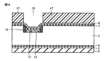
以下、図3~図17の模式的断面図を参照して、第1の実施の形態である光電変換素子1の製造方法の一例について説明する。なお、以下に示す例はあくまでも一例であり、各操作の順序は以下の例に限定されず、適宜変更することができる。
以下、図3~図17の模式的断面図を参照して、第1の実施の形態である光電変換素子1の製造方法の一例について説明する。なお、以下に示す例はあくまでも一例であり、各操作の順序は以下の例に限定されず、適宜変更することができる。
まず、図3に示すように、n型単結晶シリコンからなる半導体基板3の受光面の反対側(すなわち、裏面)に、開口部10を備えた耐アルカリ性のレジスト膜9を形成する。
ここで、レジスト膜9は、特に限定されないが、たとえば、耐アルカリ性のレジストインクをインクジェット法により、開口部10の形成箇所以外の箇所に印刷し、それを乾燥させることにより形成したものなどを用いることができる。
次に、図4に示すように、レジスト膜9の開口部10から露出している半導体基板3の裏面の一部を除去することによって、底面11aと、底面11aの両側から半導体基板3の厚さ方向に伸長する側壁11bとからなる溝11を形成する。ここでは、まずドライエッチングによって異方性をもったエッチングを行なった後、ウエットエッチングによって、ドライエッチングにより生成されたダメージ層を除去することが好ましい。
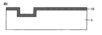
次に、レジスト膜9を除去し、洗浄した後、図5に示すように、溝11の底面11aおよび側壁11bを含む、半導体基板3の裏面全体に、絶縁膜16を形成する。絶縁膜16の形成方法は特に限定されず、従来公知のいかなる方法も採用できる。
絶縁膜16が酸化シリコン膜である場合、スチーム酸化、常圧CVD法などによっても形成することができるが、熱酸化法によって形成されることが好ましい。ここで、熱酸化法による処理温度は800℃~1100℃であることが好ましい。熱酸化法による膜形成は、簡易な方法であり、他の製法に比べ、形成される酸化シリコン膜の性質がよく、緻密であり、かつパッシベーション効果が高く好適である。ここで、形成される絶縁膜16の厚さは、処理時間によって調製可能であり、たとえば1nm以上500nm以下とすることができる。また、熱酸化処理後に、水素アニール処理を行なっても良い。ここで、水素アニール処理の処理温度は、たとえば300℃~500℃とすることができる。
また、絶縁膜16が窒化シリコン膜である場合、蒸着法などによっても形成することができるが、プラズマCVD法によって形成されることが好ましい。プラズマCVD法によって、窒化シリコン膜を形成する場合、原料ガスとしてシラン(SiH4)ガスとアンモニア(NH3)ガスとからなる混合ガスなどを用いることができる。ここで、形成される絶縁膜16の厚さは、製膜時間や製膜圧力などによって調製可能であり、たとえば1nm以上500nm以下とすることができる。
次に、図6に示すように、半導体基板3の裏面の平面部に形成された絶縁膜16を除去する。このようにすることで、溝11の側壁11bに絶縁膜16が形成された半導体基板3を得ることができる。ここで、絶縁膜16を除去する方法としては、特に限定されず、ドライエッチング、ウエットエッチングのいずれを用いても良い。
次に、図7に示すように、n型単結晶シリコンからなる半導体基板3の受光面の全面に、i型のアモルファスシリコンからなる第3の誘電体膜4およびn型のアモルファスシリコンからなる第3の半導体膜5を、この順序で、たとえばプラズマCVD法により積層する。
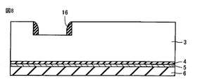
次に、図8に示すように、第3の半導体膜5の全面に反射防止膜6をたとえばスパッタリング法、CVD法、蒸着法などにより積層する。
次に、図9に示すように、溝11の側壁11bに絶縁膜16を有する半導体基板3の裏面全面に、i型のアモルファスシリコンからなる第2の誘電体膜12およびp型のアモルファスシリコンからなる第2の半導体膜13を、この順序で、たとえばプラズマCVD法により積層する。ここで、第2の半導体膜13は、p型のアモルファスシリコンからなる膜とp型のアモルファスゲルマニウムからなる膜とが積層されていても良く、その場合には、p型のアモルファスシリコンからなる膜の上にp型のアモルファスゲルマニウムからなる膜を、たとえばプラズマCVD法により積層する。
次に、図10に示すように、溝11の少なくとも一部にマスク材14を埋め込む。ここで、マスク材14による溝11の埋め込みは、たとえば、マスク材14を加熱して溶融状態とし、それをインクジェット法により、溝11を埋め込むように選択的に塗布して、冷却して固化状態とした後に乾燥させることにより行なうことができる。
ここで、マスク材14としては、第2の誘電体膜12および第2の半導体膜13のエッチングマスクとして機能するものであれば特に限定されないが、なかでもホットメルト接着剤を用いることが好ましい。なお、ホットメルト接着剤は、常温では固体状態であるが、加熱により溶融状態となり、塗布後の滲みが少ないという特性を有する。
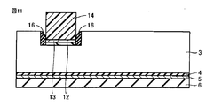
次に、図11に示すように、マスク材14によって被覆されていない第2の誘電体膜12および第2の半導体膜13を除去する。ここで、第2の誘電体膜12および第2の半導体膜13を除去する方法は特に限定されないが、ドライエッチングを用いることが好適である。
次に、図12に示すように、マスク材14を除去し、その後洗浄する。ここで、マスク材14を除去する方法は、特に限定されないが、たとえばマスク材14がホットメルト接着剤からなる場合には、マスク材14を温水に浸漬して剥離する方法などが挙げられる。
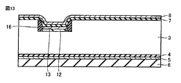
次に、図13に示すように、マスク材14を除去した後の半導体基板3の裏面の全面上に、i型のアモルファスシリコンからなる第1の誘電体膜7およびn型のアモルファスシリコンからなる第1の半導体膜8を、この順序で、たとえばプラズマCVD法により積層する。ここで、第1の半導体膜8は、n型のアモルファスシリコンからなる膜とn型のアモルファスゲルマニウムからなる膜とが積層されていても良く、その場合には、n型のアモルファスシリコンからなる膜の上にn型のアモルファスゲルマニウムからなる膜を、たとえばプラズマCVD法により積層する。
次に、図14に示すように、半導体基板3の裏面の開口部10以外の部分に、レジスト膜17を形成する。ここで、レジスト膜17は、特に限定されず、たとえば、上記で例示したものを用いることができる。
次に、図15に示すように、レジスト膜17の開口部10から露出している第1の誘電体膜7および第1の半導体膜8を除去し、溝11の中に形成された第2の半導体膜13を露出させる。ここで、第1の誘電体膜7および第1の半導体膜8を除去する方法としては、アルカリ溶液を用いたウエットエッチングを用いることが好ましい。すなわち、p型の第2の半導体膜13は、アルカリ溶液を用いたウエットエッチングでは除去され難いため、第2の半導体膜13がエッチングストップ層として機能して、第1の誘電体膜7および第1の半導体膜8を確実に除去することができる。ここで、アルカリ溶液としては、特に限定されず、たとえば、上記で例示したものを用いることができる。
次に、レジスト膜17を除去し、その後洗浄する。次に、図16に示すように半導体基板3の裏面側の全面に金属層20を形成する。ここで、金属層20は、従来公知の方法で形成することができ、たとえばCVD法、スパッタリング法、蒸着法などを好適に用いることができる。また、金属層20は、ニッケル(Ni)、コバルト(Co)、チタン(Ti)からなる群より選ばれた少なくとも1種の金属からなることが好ましく、金属層20の厚さは、たとえば0.1μm以上1.0μm以下とすることができる。
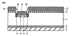
次に、図17に示すように、金属層20を形成した後、熱処理を行なうことにより、金属層20と第1の半導体膜8および第2の半導体膜13とを反応させて、金属間化合物層15を形成することができる。ここで、金属間化合物層15が金属シリサイド層からなる場合には、熱処理温度は、200℃以上600℃以下であることがより好ましい。
上記したように、第1の半導体膜8および第2の半導体膜13が、アモルファスシリコンからなる膜の上にアモルファスゲルマニウムからなる膜が積層されている場合には、金属間化合物層15を金属ジャーマナイド層とすることができる。金属間化合物層15が金属ジャーマナイド層からなる場合には、熱処理温度は100℃以上500℃以下であることが好ましい。このように、金属ジャーマナイド層は、金属シリサイド層に比べて低温で形成が可能であり好適である。
この理由は、本実施の形態のように、半導体基板に溝が形成されている場合、600℃を超える高温で熱処理を行なうと、該溝(すなわち、半導体基板の厚さが異なる部位)に起因して、半導体基板に反りなどの不具合が生じる可能性があるからである。したがって、そのような不具合の発生を抑制するためには、金属層と半導体膜とを反応させる温度は、600℃以下であること要する。金属ジャーマナイド層は、500℃以下で形成可能であり、半導体基板の反りなどの不具合の発生がなく、特に好適である。
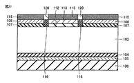
なお、図17に示すように、絶縁膜16と金属層20は熱処理によって反応しないため、絶縁膜16上の金属層20は未反応のまま残存する。
次に、図1に示すように、未反応の金属層20を除去する。ここで、未反応の金属層20を除去する方法としては、酸性溶液を用いたウエットエッチングを用いることが好ましい。第1の半導体膜8および第2の半導体膜13上に形成された金属間化合物層15は耐食性を有するため、酸性溶液を用いることにより、絶縁膜16上に残存した未反応の金属層20を選択的に除去することができる。未反応の金属層20を除去することにより、第1の半導体膜8上の金属間化合物層15と第2の半導体膜13上の金属間化合物層15とは、下地となる第1の半導体膜8および第2の半導体膜13の形状に従って分離される(すなわち、自己整合的に分離される)。これにより、金属間化合物層15はp型電極とn型電極とに分離される。
本実施の形態によれば、図44に示す構造を有する太陽電池のように、透明導電酸化膜によって半導体膜と電極層とを接続する必要がないため、接触抵抗が低減され、光電変換素子の変換効率を高めることができる。
また、本実施の形態によれば、図28~図44に示される方法のように、フォトレジストの塗布ならびにフォトリソグラフィー技術およびエッチング技術によるフォトレジストの複雑なパターンニング工程を行なう必要がないため、より簡易な製造工程で光電変換素子を製造することができる。
特に、図37~44に示される方法のように、電極形成において複雑なパターニング工程を行なう必要がなく、上記のように金属間化合物層からなる低抵抗電極が形成されるとともに、簡易かつ確実にp型電極(第2の半導体膜13の上の電極)とn型電極(第1の半導体膜8の上の電極)とを分離することができる。
また、本実施の形態においては、p型電極およびn型電極を半導体基板の厚さ方向の異なる位置に形成しているため、半導体基板の裏面におけるp型電極とn型電極との間の隙間を小さくすることができるとともに、このような隙間の小さいp型電極とn型電極とを形成するための精密なパターンニングをする必要がない。ここで、アモルファス膜(第1の半導体膜8および第2の半導体膜13)は水平方向(膜の面方向)には電流が流れにくいため、半導体基板の裏面のp型電極とn型電極との間の隙間はできるだけ小さい方が高い変換効率を有する光電変換素子を得る観点からは好ましい。そして、本実施の形態においては、上記のようにp型電極とn型電極とを、裏面に形成された溝および溝側壁に形成された絶縁膜によって、電気的に分離するため、電気的に分離が不十分な場合に生じる変換効率の低下が防止される。
さらに、本実施の形態においては、半導体基板の裏面の全平面をp型電極とn型電極とで覆うことができるため、半導体基板の受光面側から入射した光のうち吸収されずに半導体基板の裏面側に透過してきた光をp型電極およびn型電極で反射することができる。また、溝側壁に形成された絶縁膜により、溝側壁に透過してきた光をも反射することができる。
またさらに、本実施の形態においては、半導体基板の溝の底面を含む、半導体基板の裏面の全平面がi型の誘電体膜、n型の半導体膜およびp型の半導体膜によってパッシベーションされており、加えて溝の底面の一部および側壁も絶縁膜によってパッシベーションされている。したがって、半導体基板の裏面全体において良好なパッシベーション特性を得ることができ、半導体基板の表面でのキャリア再結合を抑制することができる。
以上の理由により、本実施の形態においては、図44に示す構造を有する太陽電池よりも高い変換効率を有する光電変換素子を得ることができる。また、本実施の形態においては、高い変換効率を有する光電変換素子を簡易な製造工程で製造することができる。
<実施の形態2>
[光電変換素子]
≪全体構成≫
図2に、本発明の第2の実施の形態である光電変換素子2の模式的な断面図を示す。光電変換素子2は、半導体基板103の裏面に溝を有しておらず、半導体基板103の裏面の表面上に、i型のアモルファスシリコンからなる第1の誘電体膜107と第2の誘電体膜112とが離間して設けられている。また、第1の誘電体膜107上には、n型のアモルファスシリコンからなる第1の半導体膜108が設けられている。また、第2の誘電体膜112上には、p型のアモルファスシリコンからなる第2の半導体膜113が設けられている。そして、第1の半導体膜108および第2の半導体膜113の裏面の全面上には、金属間化合物層115が設けられている。
[光電変換素子]
≪全体構成≫
図2に、本発明の第2の実施の形態である光電変換素子2の模式的な断面図を示す。光電変換素子2は、半導体基板103の裏面に溝を有しておらず、半導体基板103の裏面の表面上に、i型のアモルファスシリコンからなる第1の誘電体膜107と第2の誘電体膜112とが離間して設けられている。また、第1の誘電体膜107上には、n型のアモルファスシリコンからなる第1の半導体膜108が設けられている。また、第2の誘電体膜112上には、p型のアモルファスシリコンからなる第2の半導体膜113が設けられている。そして、第1の半導体膜108および第2の半導体膜113の裏面の全面上には、金属間化合物層115が設けられている。
また、第1の誘電体膜107と第2の誘電体膜112との間には、絶縁膜116が設けられている。ここで、絶縁膜116は、第1の誘電体膜107の側面部および/または第2の誘電体膜112の側面部と接して形成されている。また、絶縁膜116は、第1の半導体膜108の側面部および/または第2の半導体膜113の側面部と接していても良い。
光電変換素子2の受光面(裏面の反対側の面)には、光電変換素子1と同様に、第3の誘電体膜104、第3の半導体膜105および反射防止膜106が設けられている。ここで、光電変換素子2を構成する半導体基板、各膜、各層の材質および厚さは、たとえば、光電変換素子1の説明において、例示したものを用いることができる。
なお、光電変換素子2においては、第1の半導体膜108がn型であり、かつ第2の半導体膜113がp型である構成を例示するが、第1の半導体膜がp型であり、かつ第2の半導体膜がn型であっても本発明の効果は示される。
また、光電変換素子1においては、受光面に第3の半導体膜105が設けられた構成を例示するが、第3の半導体膜105は必ずしも必須の要素ではなく、第3の半導体膜105を有しない構成であったとしても、本発明の効果は示されるものとする。
このような本実施の形態の光電変換素子は、以下のような製造方法によって製造される。換言すれば、以下のような製造方法によって製造される光電変換素子は、上記のような特性を示す。したがって、本実施の形態の光電変換素子は、発電効率を向上させるとともに、簡易な製造工程で製造することができる光電変換素子である。
[光電変換素子の製造方法]
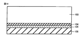
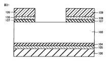
以下、図18~図27の模式的断面図を参照して、第2の実施の形態である光電変換素子2の製造方法の一例について説明する。なお、以下に示す例はあくまでも一例であり、各操作の順序は以下の例に限定されず、適宜変更することができる。
以下、図18~図27の模式的断面図を参照して、第2の実施の形態である光電変換素子2の製造方法の一例について説明する。なお、以下に示す例はあくまでも一例であり、各操作の順序は以下の例に限定されず、適宜変更することができる。
まず、図18に示すように、n型単結晶シリコンからなる半導体基板103の受光面の全面に、i型のアモルファスシリコンからなる第3の誘電体膜104およびn型のアモルファスシリコンからなる第3の半導体膜105および反射防止膜106を、この順序で、たとえばプラズマCVD法により積層する。
次に、図19に示すように、半導体基板103の裏面の全面上に、i型のアモルファスシリコンからなる第1の誘電体膜107およびn型のアモルファスシリコンからなる第1の半導体膜108を、この順序で、たとえばプラズマCVD法により積層する。ここで、第1の半導体膜108は、n型のアモルファスシリコンからなる膜とn型のアモルファスゲルマニウムからなる膜とが積層されていても良く、その場合には、n型のアモルファスシリコンからなる膜の上にn型のアモルファスゲルマニウムからなる膜を、たとえばプラズマCVD法により積層する。
次に、図20に示すように、開口部110を備えたレジスト膜109を形成する。ここで、レジスト膜109は、特に限定されず、たとえば上記で耐アルカリ性のレジスト膜として例示したものを用いることができる。
次に、図21に示すように、レジスト膜109で被覆されていない第1の誘電体膜107および第1の誘電体膜108の一部を除去し、半導体基板103を露出させる。ここで、第1の誘電体膜107および第1の半導体膜108を除去する方法は特に限定されないが、アルカリ溶液を用いたウエットエッチングを用いることが好ましい。
次に、レジスト膜109を除去して洗浄した後、図22に示すように、第1の半導体膜108の裏面全面上および半導体基板103の裏面全面上に、絶縁膜116を形成する。ここで、絶縁膜116を形成する方法は、たとえば、上記で例示した方法を用いることができる。また、絶縁膜116としては、熱酸化シリコン膜、窒化シリコン膜が好ましい。
次に、図23に示すように、平面上に形成された絶縁膜116を除去することにより、第1の誘電体膜107および第1の半導体膜108の側面部に絶縁膜116を残存させる。絶縁膜116を除去する方法は特に限定されず、ドライエッチング、ウエットエッチングのいずれを用いても良い。
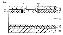
次に、図24に示すように、第1の半導体膜108の裏面全面上、半導体基板103の裏面全面上および絶縁膜116の残部上に、i型のアモルファスシリコンからなる第2の誘電体膜112およびp型のアモルファスシリコンからなる第2の半導体膜113を、この順序で、たとえばプラズマCVD法により積層する。ここで、第2の半導体膜113は、p型のアモルファスシリコンからなる膜とp型のアモルファスゲルマニウムからなる膜とが積層されていても良く、その場合には、p型のアモルファスシリコンからなる膜の上にp型のアモルファスゲルマニウムからなる膜を、たとえばプラズマCVD法により積層する。
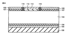
次に、図25に示すように、第1の半導体膜108上および絶縁膜116の残部上に形成された第2の誘電体膜112および第2の半導体膜113を除去する。ここで、第2の誘電体膜112および第2の半導体膜113を除去する方法としては、たとえば上記で例示したようにドライエッチングなどを用いることができる。
次に、図26に示すように、第1の半導体膜108上、第2の半導体膜113上および絶縁膜116の残部上に、金属層120を形成する。ここで、金属層120を形成する方法としては、上記で例示したようにスパッタリング法などを用いることができ、金属層120は、ニッケル(Ni)、コバルト(Co)、チタン(Ti)からなる群より選ばれた少なくとも1種の金属からなることが好ましい。
次に、図27に示すように、熱処理を行なうことにより、金属層120と第1の半導体膜108および第2の半導体膜113とを反応させて、金属間化合物層115を形成する。ここで、絶縁膜116と金属層120は熱処理によって反応しないため、絶縁膜116上の金属層120は未反応のまま残存する。
次に、図2に示すように、絶縁膜116上の未反応の金属層120を除去することによって、金属間化合物層115はp型電極とn型電極とに自己整合的に分離される。
本実施の形態によれば、図44に示す構造を有する太陽電池のように、透明導電酸化膜によって半導体膜と電極層を接続する必要がないため、接触抵抗が低減され、光電変換素子の変換効率を高めることができる。
また、本実施の形態によれば、図37~44に示される方法のように、電極形成において複雑なパターニング工程を行なう必要がなく、上記のように金属間化合物層からなる低抵抗電極が形成されるとともに、簡易かつ確実にp型電極(第2の半導体膜113の上の電極)とn型電極(第1の半導体膜107の上の電極)とを分離することができる。
またさらに、本実施の形態においては、半導体基板の裏面の全平面がi型の誘電体膜、n型の半導体膜、p型の半導体膜および絶縁膜によってパッシベーションされており、半導体基板の裏面全体において良好なパッシベーション特性を得ることができ、半導体基板の表面でのキャリア再結合を抑制することができる。
以上の理由により、本実施の形態においては、図44に示す構造を有する太陽電池よりも高い変換効率を有する光電変換素子を得ることができる。また、本実施の形態においては、高い変換効率を有する光電変換素子を簡易な製造工程で製造することができる。
以上のように本発明の実施の形態について説明を行なったが、上述の各実施の形態の構成を適宜組み合わせることも当初から予定している。
今回開示された実施の形態はすべての点で例示であって制限的なものではないと考えられるべきである。本発明の範囲は上記した説明ではなくて請求の範囲によって示され、請求の範囲と均等の意味および範囲内でのすべての変更が含まれることが意図される。
本発明は、光電変換素子および光電変換素子の製造方法に利用することができる。
1,2 光電変換素子、3,103 半導体基板、4,104 第3の誘電体膜、5,105 第3の半導体膜、6,106 反射防止膜、7,107 第1の誘電体膜、8,108 第1の半導体膜、9,17,109 レジスト膜、10,110 開口部、11 溝、11a 底面、11b 側壁、12,112 第2の誘電体膜、13,113 第2の半導体膜、14 マスク材、15,115 金属間化合物層、16,116 絶縁膜、20,120 金属層、901 c-Si(n)基板、902 a-Si(i/p)層、903 a-Si(i/n)層、904 フォトレジスト膜、905 a-Si(i/n)層、906 フォトレジスト膜、907 透明導電酸化膜、908,909 フォトレジスト膜、910 裏面電極層、911 反射防止膜。
Claims (5)
- 第1導電型の半導体基板と、
前記半導体基板の一方の表面上に設けられた第1導電型の第1の半導体膜と、
前記表面上に前記第1の半導体膜から独立して設けられた第2導電型の第2の半導体膜と、
前記半導体基板と前記第1の半導体膜との間および前記半導体基板と前記第2の半導体膜との間の少なくともいずれかに設けられた誘電体膜と、を備え、
前記第1の半導体膜上および前記第2の半導体膜上に金属間化合物層が形成されている、光電変換素子。 - 前記半導体基板の前記表面には溝が設けられており、
前記溝の底面に前記第2の半導体膜が設けられている、請求項1に記載の光電変換素子。 - 前記半導体基板の一方の表面上において、前記第1の半導体膜と前記第2の半導体膜とは離間して設けられており、
前記第1の半導体膜と前記第2の半導体膜との間に絶縁膜が設けられている、請求項1に記載の光電変換素子。 - 前記金属間化合物層は、金属シリサイド層および金属ジャーマナイド層の少なくともいずれかである、請求項1~請求項3のいずれか1項に記載の光電変換素子。
- 前記金属ジャーマナイド層は、ニッケル、コバルトおよびチタンからなる群より選ばれた少なくとも1種の金属とゲルマニウムとからなる化合物層である、請求項4に記載の光電変換素子。
Priority Applications (2)
| Application Number | Priority Date | Filing Date | Title |
|---|---|---|---|
| US14/427,054 US20150221791A1 (en) | 2012-09-25 | 2013-09-19 | Photoelectric conversion element |
| CN201380049644.3A CN104685639B (zh) | 2012-09-25 | 2013-09-19 | 光电转换元件 |
Applications Claiming Priority (2)
| Application Number | Priority Date | Filing Date | Title |
|---|---|---|---|
| JP2012210904A JP2014067804A (ja) | 2012-09-25 | 2012-09-25 | 光電変換素子 |
| JP2012-210904 | 2012-09-25 |
Publications (1)
| Publication Number | Publication Date |
|---|---|
| WO2014050685A1 true WO2014050685A1 (ja) | 2014-04-03 |
Family
ID=50388090
Family Applications (1)
| Application Number | Title | Priority Date | Filing Date |
|---|---|---|---|
| PCT/JP2013/075262 Ceased WO2014050685A1 (ja) | 2012-09-25 | 2013-09-19 | 光電変換素子 |
Country Status (3)
| Country | Link |
|---|---|
| US (1) | US20150221791A1 (ja) |
| JP (1) | JP2014067804A (ja) |
| WO (1) | WO2014050685A1 (ja) |
Cited By (2)
| Publication number | Priority date | Publication date | Assignee | Title |
|---|---|---|---|---|
| KR20240022536A (ko) * | 2021-06-04 | 2024-02-20 | 솔라랩 아이코 유럽 게엠베하 | 선택적 접촉 영역 매립형 태양 전지 및 그 배면 접촉 구조 |
| JP2024509329A (ja) * | 2021-06-04 | 2024-02-29 | ソーラーラボ アイコ ヨーロッパ ゲーエムベーハー | 選択的接触領域埋込型太陽電池及びその裏面接触構造 |
Families Citing this family (5)
| Publication number | Priority date | Publication date | Assignee | Title |
|---|---|---|---|---|
| JP6333139B2 (ja) * | 2014-09-18 | 2018-05-30 | シャープ株式会社 | 光電変換素子および光電変換素子の製造方法 |
| EP3340315B1 (en) | 2015-08-21 | 2021-10-27 | Sharp Kabushiki Kaisha | Photoelectric conversion element |
| US10692986B2 (en) | 2016-06-17 | 2020-06-23 | National Institute Of Advanced Industrial Science And Technology | Compound film of tungsten and germanium, and semiconductor device |
| US10741705B2 (en) * | 2017-07-14 | 2020-08-11 | The Board Of Trustees Of The University Of Illinois | Optoelectronic device having an antireflective surface |
| JP2023120673A (ja) * | 2022-02-18 | 2023-08-30 | 株式会社カネカ | 太陽電池及び太陽電池製造方法 |
Citations (5)
| Publication number | Priority date | Publication date | Assignee | Title |
|---|---|---|---|---|
| JP2004266023A (ja) * | 2003-02-28 | 2004-09-24 | Sharp Corp | 太陽電池およびその製造方法 |
| JP2005101240A (ja) * | 2003-09-24 | 2005-04-14 | Sanyo Electric Co Ltd | 光起電力素子およびその製造方法 |
| JP2011061020A (ja) * | 2009-09-10 | 2011-03-24 | Sharp Corp | 裏面コンタクト型太陽電池素子およびその製造方法 |
| WO2011093329A1 (ja) * | 2010-01-26 | 2011-08-04 | 三洋電機株式会社 | 太陽電池及びその製造方法 |
| WO2011121776A1 (ja) * | 2010-03-31 | 2011-10-06 | 株式会社 東芝 | 半導体装置の製造方法 |
Family Cites Families (3)
| Publication number | Priority date | Publication date | Assignee | Title |
|---|---|---|---|---|
| WO2010087853A1 (en) * | 2009-01-30 | 2010-08-05 | Hewlett-Packard Development Company | Photovoltaic structure and solar cell and method of fabrication employing hidden electrode |
| KR101196793B1 (ko) * | 2010-08-25 | 2012-11-05 | 엘지전자 주식회사 | 태양 전지 및 그 제조 방법 |
| KR20130050721A (ko) * | 2011-11-08 | 2013-05-16 | 삼성에스디아이 주식회사 | 태양 전지 |
-
2012
- 2012-09-25 JP JP2012210904A patent/JP2014067804A/ja active Pending
-
2013
- 2013-09-19 WO PCT/JP2013/075262 patent/WO2014050685A1/ja not_active Ceased
- 2013-09-19 US US14/427,054 patent/US20150221791A1/en not_active Abandoned
Patent Citations (5)
| Publication number | Priority date | Publication date | Assignee | Title |
|---|---|---|---|---|
| JP2004266023A (ja) * | 2003-02-28 | 2004-09-24 | Sharp Corp | 太陽電池およびその製造方法 |
| JP2005101240A (ja) * | 2003-09-24 | 2005-04-14 | Sanyo Electric Co Ltd | 光起電力素子およびその製造方法 |
| JP2011061020A (ja) * | 2009-09-10 | 2011-03-24 | Sharp Corp | 裏面コンタクト型太陽電池素子およびその製造方法 |
| WO2011093329A1 (ja) * | 2010-01-26 | 2011-08-04 | 三洋電機株式会社 | 太陽電池及びその製造方法 |
| WO2011121776A1 (ja) * | 2010-03-31 | 2011-10-06 | 株式会社 東芝 | 半導体装置の製造方法 |
Cited By (4)
| Publication number | Priority date | Publication date | Assignee | Title |
|---|---|---|---|---|
| KR20240022536A (ko) * | 2021-06-04 | 2024-02-20 | 솔라랩 아이코 유럽 게엠베하 | 선택적 접촉 영역 매립형 태양 전지 및 그 배면 접촉 구조 |
| JP2024509329A (ja) * | 2021-06-04 | 2024-02-29 | ソーラーラボ アイコ ヨーロッパ ゲーエムベーハー | 選択的接触領域埋込型太陽電池及びその裏面接触構造 |
| JP7649877B2 (ja) | 2021-06-04 | 2025-03-21 | ソーラーラボ アイコ ヨーロッパ ゲーエムベーハー | 選択的接触領域埋込型太陽電池及びその裏面接触構造 |
| KR102891080B1 (ko) | 2021-06-04 | 2025-11-25 | 솔라랩 아이코 유럽 게엠베하 | 선택적 접촉 영역 매립형 태양 전지 및 그 배면 접촉 구조 |
Also Published As
| Publication number | Publication date |
|---|---|
| US20150221791A1 (en) | 2015-08-06 |
| CN104685639A (zh) | 2015-06-03 |
| JP2014067804A (ja) | 2014-04-17 |
Similar Documents
| Publication | Publication Date | Title |
|---|---|---|
| US12532569B2 (en) | Metallization of solar cells | |
| US8779280B2 (en) | Solar cell and method of manufacturing the same | |
| US8603851B2 (en) | Solar cell and method of manufacturing the same by simultaneously forming first and second doping regions | |
| JP5213134B2 (ja) | 太陽電池 | |
| WO2014050685A1 (ja) | 光電変換素子 | |
| JP6178400B2 (ja) | ワイドバンドギャップ半導体材料含有のエミッタ領域を有する太陽電池 | |
| JP2004266023A (ja) | 太陽電池およびその製造方法 | |
| TW200947725A (en) | Improved HIT solar cell structure | |
| EP2811539B1 (en) | Solar cell with multilayered structure and manufacturing method thereof | |
| TWI685117B (zh) | 具結晶矽且光接收表面鈍化之太陽能電池及其製造方法 | |
| CN102356466A (zh) | 制造接触的方法、接触和包括接触的太阳能电池 | |
| CN217306520U (zh) | 太阳能电池和光伏组件 | |
| JP6783231B2 (ja) | 光電変換素子 | |
| JP7664372B2 (ja) | 太陽電池および光起電力モジュール | |
| WO2026056632A1 (zh) | 一种背接触电池的制造方法 | |
| KR20190082109A (ko) | 태양 전지의 다결정 실리콘 피처를 위한 전도성 접촉자 | |
| CN103210499B (zh) | 电接触 | |
| WO2015064354A1 (ja) | 太陽電池 | |
| JP2015506584A (ja) | 光起電力セル及び製造方法 | |
| KR20100094224A (ko) | 태양전지 및 이의 제조방법 | |
| JP6033624B2 (ja) | 光電変換素子 | |
| JP5224470B2 (ja) | 光電変換部材 | |
| CN104685639B (zh) | 光电转换元件 | |
| WO2012169277A1 (ja) | テクスチャ構造の形成方法および太陽電池の製造方法 | |
| CN120512956A (zh) | 一种太阳能电池、光伏组件和太阳能电池的制作方法 |
Legal Events
| Date | Code | Title | Description |
|---|---|---|---|
| 121 | Ep: the epo has been informed by wipo that ep was designated in this application |
Ref document number: 13841736 Country of ref document: EP Kind code of ref document: A1 |
|
| WWE | Wipo information: entry into national phase |
Ref document number: 14427054 Country of ref document: US |
|
| NENP | Non-entry into the national phase |
Ref country code: DE |
|
| 122 | Ep: pct application non-entry in european phase |
Ref document number: 13841736 Country of ref document: EP Kind code of ref document: A1 |