US10692986B2 - Compound film of tungsten and germanium, and semiconductor device - Google Patents
Compound film of tungsten and germanium, and semiconductor device Download PDFInfo
- Publication number
- US10692986B2 US10692986B2 US16/302,441 US201716302441A US10692986B2 US 10692986 B2 US10692986 B2 US 10692986B2 US 201716302441 A US201716302441 A US 201716302441A US 10692986 B2 US10692986 B2 US 10692986B2
- Authority
- US
- United States
- Prior art keywords
- germanium
- tungsten
- compound
- substrate
- compound film
- Prior art date
- Legal status (The legal status is an assumption and is not a legal conclusion. Google has not performed a legal analysis and makes no representation as to the accuracy of the status listed.)
- Active
Links
Images


Classifications
-
- H01L29/45—
-
- B—PERFORMING OPERATIONS; TRANSPORTING
- B82—NANOTECHNOLOGY
- B82Y—SPECIFIC USES OR APPLICATIONS OF NANOSTRUCTURES; MEASUREMENT OR ANALYSIS OF NANOSTRUCTURES; MANUFACTURE OR TREATMENT OF NANOSTRUCTURES
- B82Y10/00—Nanotechnology for information processing, storage or transmission, e.g. quantum computing or single electron logic
-
- C—CHEMISTRY; METALLURGY
- C23—COATING METALLIC MATERIAL; COATING MATERIAL WITH METALLIC MATERIAL; CHEMICAL SURFACE TREATMENT; DIFFUSION TREATMENT OF METALLIC MATERIAL; COATING BY VACUUM EVAPORATION, BY SPUTTERING, BY ION IMPLANTATION OR BY CHEMICAL VAPOUR DEPOSITION, IN GENERAL; INHIBITING CORROSION OF METALLIC MATERIAL OR INCRUSTATION IN GENERAL
- C23C—COATING METALLIC MATERIAL; COATING MATERIAL WITH METALLIC MATERIAL; SURFACE TREATMENT OF METALLIC MATERIAL BY DIFFUSION INTO THE SURFACE, BY CHEMICAL CONVERSION OR SUBSTITUTION; COATING BY VACUUM EVAPORATION, BY SPUTTERING, BY ION IMPLANTATION OR BY CHEMICAL VAPOUR DEPOSITION, IN GENERAL
- C23C16/00—Chemical coating by decomposition of gaseous compounds, without leaving reaction products of surface material in the coating, i.e. chemical vapour deposition [CVD] processes
- C23C16/06—Chemical coating by decomposition of gaseous compounds, without leaving reaction products of surface material in the coating, i.e. chemical vapour deposition [CVD] processes characterised by the deposition of metallic material
- C23C16/08—Chemical coating by decomposition of gaseous compounds, without leaving reaction products of surface material in the coating, i.e. chemical vapour deposition [CVD] processes characterised by the deposition of metallic material from metal halides
-
- C—CHEMISTRY; METALLURGY
- C23—COATING METALLIC MATERIAL; COATING MATERIAL WITH METALLIC MATERIAL; CHEMICAL SURFACE TREATMENT; DIFFUSION TREATMENT OF METALLIC MATERIAL; COATING BY VACUUM EVAPORATION, BY SPUTTERING, BY ION IMPLANTATION OR BY CHEMICAL VAPOUR DEPOSITION, IN GENERAL; INHIBITING CORROSION OF METALLIC MATERIAL OR INCRUSTATION IN GENERAL
- C23C—COATING METALLIC MATERIAL; COATING MATERIAL WITH METALLIC MATERIAL; SURFACE TREATMENT OF METALLIC MATERIAL BY DIFFUSION INTO THE SURFACE, BY CHEMICAL CONVERSION OR SUBSTITUTION; COATING BY VACUUM EVAPORATION, BY SPUTTERING, BY ION IMPLANTATION OR BY CHEMICAL VAPOUR DEPOSITION, IN GENERAL
- C23C16/00—Chemical coating by decomposition of gaseous compounds, without leaving reaction products of surface material in the coating, i.e. chemical vapour deposition [CVD] processes
- C23C16/44—Chemical coating by decomposition of gaseous compounds, without leaving reaction products of surface material in the coating, i.e. chemical vapour deposition [CVD] processes characterised by the method of coating
- C23C16/455—Chemical coating by decomposition of gaseous compounds, without leaving reaction products of surface material in the coating, i.e. chemical vapour deposition [CVD] processes characterised by the method of coating characterised by the method used for introducing gases into reaction chamber or for modifying gas flows in reaction chamber
- C23C16/45557—Pulsed pressure or control pressure
-
- H01L21/28—
-
- H01L21/285—
-
- H01L21/28568—
-
- H01L29/417—
-
- H01L29/456—
-
- H01L29/78—
-
- H01L29/786—
-
- H—ELECTRICITY
- H10—SEMICONDUCTOR DEVICES; ELECTRIC SOLID-STATE DEVICES NOT OTHERWISE PROVIDED FOR
- H10D—INORGANIC ELECTRIC SEMICONDUCTOR DEVICES
- H10D30/00—Field-effect transistors [FET]
- H10D30/01—Manufacture or treatment
- H10D30/014—Manufacture or treatment of FETs having zero-dimensional [0D] or one-dimensional [1D] channels, e.g. quantum wire FETs, single-electron transistors [SET] or Coulomb blockade transistors
-
- H—ELECTRICITY
- H10—SEMICONDUCTOR DEVICES; ELECTRIC SOLID-STATE DEVICES NOT OTHERWISE PROVIDED FOR
- H10D—INORGANIC ELECTRIC SEMICONDUCTOR DEVICES
- H10D30/00—Field-effect transistors [FET]
- H10D30/01—Manufacture or treatment
- H10D30/021—Manufacture or treatment of FETs having insulated gates [IGFET]
- H10D30/024—Manufacture or treatment of FETs having insulated gates [IGFET] of fin field-effect transistors [FinFET]
-
- H—ELECTRICITY
- H10—SEMICONDUCTOR DEVICES; ELECTRIC SOLID-STATE DEVICES NOT OTHERWISE PROVIDED FOR
- H10D—INORGANIC ELECTRIC SEMICONDUCTOR DEVICES
- H10D30/00—Field-effect transistors [FET]
- H10D30/01—Manufacture or treatment
- H10D30/021—Manufacture or treatment of FETs having insulated gates [IGFET]
- H10D30/027—Manufacture or treatment of FETs having insulated gates [IGFET] of lateral single-gate IGFETs
-
- H—ELECTRICITY
- H10—SEMICONDUCTOR DEVICES; ELECTRIC SOLID-STATE DEVICES NOT OTHERWISE PROVIDED FOR
- H10D—INORGANIC ELECTRIC SEMICONDUCTOR DEVICES
- H10D30/00—Field-effect transistors [FET]
- H10D30/01—Manufacture or treatment
- H10D30/021—Manufacture or treatment of FETs having insulated gates [IGFET]
- H10D30/031—Manufacture or treatment of FETs having insulated gates [IGFET] of thin-film transistors [TFT]
- H10D30/0321—Manufacture or treatment of FETs having insulated gates [IGFET] of thin-film transistors [TFT] comprising silicon, e.g. amorphous silicon or polysilicon
- H10D30/0323—Manufacture or treatment of FETs having insulated gates [IGFET] of thin-film transistors [TFT] comprising silicon, e.g. amorphous silicon or polysilicon comprising monocrystalline silicon
-
- H—ELECTRICITY
- H10—SEMICONDUCTOR DEVICES; ELECTRIC SOLID-STATE DEVICES NOT OTHERWISE PROVIDED FOR
- H10D—INORGANIC ELECTRIC SEMICONDUCTOR DEVICES
- H10D30/00—Field-effect transistors [FET]
- H10D30/60—Insulated-gate field-effect transistors [IGFET]
-
- H—ELECTRICITY
- H10—SEMICONDUCTOR DEVICES; ELECTRIC SOLID-STATE DEVICES NOT OTHERWISE PROVIDED FOR
- H10D—INORGANIC ELECTRIC SEMICONDUCTOR DEVICES
- H10D30/00—Field-effect transistors [FET]
- H10D30/60—Insulated-gate field-effect transistors [IGFET]
- H10D30/62—Fin field-effect transistors [FinFET]
- H10D30/6219—Fin field-effect transistors [FinFET] characterised by the source or drain electrodes
-
- H—ELECTRICITY
- H10—SEMICONDUCTOR DEVICES; ELECTRIC SOLID-STATE DEVICES NOT OTHERWISE PROVIDED FOR
- H10D—INORGANIC ELECTRIC SEMICONDUCTOR DEVICES
- H10D30/00—Field-effect transistors [FET]
- H10D30/60—Insulated-gate field-effect transistors [IGFET]
- H10D30/67—Thin-film transistors [TFT]
-
- H—ELECTRICITY
- H10—SEMICONDUCTOR DEVICES; ELECTRIC SOLID-STATE DEVICES NOT OTHERWISE PROVIDED FOR
- H10D—INORGANIC ELECTRIC SEMICONDUCTOR DEVICES
- H10D30/00—Field-effect transistors [FET]
- H10D30/60—Insulated-gate field-effect transistors [IGFET]
- H10D30/67—Thin-film transistors [TFT]
- H10D30/6729—Thin-film transistors [TFT] characterised by the electrodes
- H10D30/6737—Thin-film transistors [TFT] characterised by the electrodes characterised by the electrode materials
-
- H—ELECTRICITY
- H10—SEMICONDUCTOR DEVICES; ELECTRIC SOLID-STATE DEVICES NOT OTHERWISE PROVIDED FOR
- H10D—INORGANIC ELECTRIC SEMICONDUCTOR DEVICES
- H10D30/00—Field-effect transistors [FET]
- H10D30/60—Insulated-gate field-effect transistors [IGFET]
- H10D30/67—Thin-film transistors [TFT]
- H10D30/674—Thin-film transistors [TFT] characterised by the active materials
- H10D30/6741—Group IV materials, e.g. germanium or silicon carbide
- H10D30/6743—Silicon
- H10D30/6744—Monocrystalline silicon
-
- H—ELECTRICITY
- H10—SEMICONDUCTOR DEVICES; ELECTRIC SOLID-STATE DEVICES NOT OTHERWISE PROVIDED FOR
- H10D—INORGANIC ELECTRIC SEMICONDUCTOR DEVICES
- H10D30/00—Field-effect transistors [FET]
- H10D30/60—Insulated-gate field-effect transistors [IGFET]
- H10D30/67—Thin-film transistors [TFT]
- H10D30/6757—Thin-film transistors [TFT] characterised by the structure of the channel, e.g. transverse or longitudinal shape or doping profile
-
- H—ELECTRICITY
- H10—SEMICONDUCTOR DEVICES; ELECTRIC SOLID-STATE DEVICES NOT OTHERWISE PROVIDED FOR
- H10D—INORGANIC ELECTRIC SEMICONDUCTOR DEVICES
- H10D62/00—Semiconductor bodies, or regions thereof, of devices having potential barriers
- H10D62/10—Shapes, relative sizes or dispositions of the regions of the semiconductor bodies; Shapes of the semiconductor bodies
- H10D62/117—Shapes of semiconductor bodies
- H10D62/118—Nanostructure semiconductor bodies
- H10D62/119—Nanowire, nanosheet or nanotube semiconductor bodies
- H10D62/121—Nanowire, nanosheet or nanotube semiconductor bodies oriented parallel to substrates
-
- H—ELECTRICITY
- H10—SEMICONDUCTOR DEVICES; ELECTRIC SOLID-STATE DEVICES NOT OTHERWISE PROVIDED FOR
- H10D—INORGANIC ELECTRIC SEMICONDUCTOR DEVICES
- H10D62/00—Semiconductor bodies, or regions thereof, of devices having potential barriers
- H10D62/80—Semiconductor bodies, or regions thereof, of devices having potential barriers characterised by the materials
- H10D62/83—Semiconductor bodies, or regions thereof, of devices having potential barriers characterised by the materials being Group IV materials, e.g. B-doped Si or undoped Ge
-
- H—ELECTRICITY
- H10—SEMICONDUCTOR DEVICES; ELECTRIC SOLID-STATE DEVICES NOT OTHERWISE PROVIDED FOR
- H10D—INORGANIC ELECTRIC SEMICONDUCTOR DEVICES
- H10D64/00—Electrodes of devices having potential barriers
- H10D64/01—Manufacture or treatment
- H10D64/011—Manufacture or treatment of electrodes ohmically coupled to a semiconductor
- H10D64/0111—Manufacture or treatment of electrodes ohmically coupled to a semiconductor to Group IV semiconductors
- H10D64/0112—Manufacture or treatment of electrodes ohmically coupled to a semiconductor to Group IV semiconductors using conductive layers comprising silicides
-
- H—ELECTRICITY
- H10—SEMICONDUCTOR DEVICES; ELECTRIC SOLID-STATE DEVICES NOT OTHERWISE PROVIDED FOR
- H10D—INORGANIC ELECTRIC SEMICONDUCTOR DEVICES
- H10D64/00—Electrodes of devices having potential barriers
- H10D64/01—Manufacture or treatment
- H10D64/011—Manufacture or treatment of electrodes ohmically coupled to a semiconductor
- H10D64/0111—Manufacture or treatment of electrodes ohmically coupled to a semiconductor to Group IV semiconductors
- H10D64/0113—Manufacture or treatment of electrodes ohmically coupled to a semiconductor to Group IV semiconductors the conductive layers comprising highly doped semiconductor materials, e.g. polysilicon layers or amorphous silicon layers
-
- H—ELECTRICITY
- H10—SEMICONDUCTOR DEVICES; ELECTRIC SOLID-STATE DEVICES NOT OTHERWISE PROVIDED FOR
- H10D—INORGANIC ELECTRIC SEMICONDUCTOR DEVICES
- H10D64/00—Electrodes of devices having potential barriers
- H10D64/20—Electrodes characterised by their shapes, relative sizes or dispositions
- H10D64/23—Electrodes carrying the current to be rectified, amplified, oscillated or switched, e.g. sources, drains, anodes or cathodes
- H10D64/251—Source or drain electrodes for field-effect devices
-
- H—ELECTRICITY
- H10—SEMICONDUCTOR DEVICES; ELECTRIC SOLID-STATE DEVICES NOT OTHERWISE PROVIDED FOR
- H10D—INORGANIC ELECTRIC SEMICONDUCTOR DEVICES
- H10D64/00—Electrodes of devices having potential barriers
- H10D64/60—Electrodes characterised by their materials
- H10D64/62—Electrodes ohmically coupled to a semiconductor
-
- H—ELECTRICITY
- H10—SEMICONDUCTOR DEVICES; ELECTRIC SOLID-STATE DEVICES NOT OTHERWISE PROVIDED FOR
- H10P—GENERIC PROCESSES OR APPARATUS FOR THE MANUFACTURE OR TREATMENT OF DEVICES COVERED BY CLASS H10
- H10P14/00—Formation of materials, e.g. in the shape of layers or pillars
- H10P14/20—Formation of materials, e.g. in the shape of layers or pillars of semiconductor materials
- H10P14/34—Deposited materials, e.g. layers
- H10P14/3402—Deposited materials, e.g. layers characterised by the chemical composition
- H10P14/3404—Deposited materials, e.g. layers characterised by the chemical composition being Group IVA materials
- H10P14/3411—Silicon, silicon germanium or germanium
-
- H—ELECTRICITY
- H10—SEMICONDUCTOR DEVICES; ELECTRIC SOLID-STATE DEVICES NOT OTHERWISE PROVIDED FOR
- H10P—GENERIC PROCESSES OR APPARATUS FOR THE MANUFACTURE OR TREATMENT OF DEVICES COVERED BY CLASS H10
- H10P14/00—Formation of materials, e.g. in the shape of layers or pillars
- H10P14/40—Formation of materials, e.g. in the shape of layers or pillars of conductive or resistive materials
- H10P14/418—Formation of materials, e.g. in the shape of layers or pillars of conductive or resistive materials the conductive layers comprising transition metals
-
- H—ELECTRICITY
- H10—SEMICONDUCTOR DEVICES; ELECTRIC SOLID-STATE DEVICES NOT OTHERWISE PROVIDED FOR
- H10P—GENERIC PROCESSES OR APPARATUS FOR THE MANUFACTURE OR TREATMENT OF DEVICES COVERED BY CLASS H10
- H10P14/00—Formation of materials, e.g. in the shape of layers or pillars
- H10P14/40—Formation of materials, e.g. in the shape of layers or pillars of conductive or resistive materials
- H10P14/42—Formation of materials, e.g. in the shape of layers or pillars of conductive or resistive materials using a gas or vapour
- H10P14/43—Chemical deposition, e.g. chemical vapour deposition [CVD]
-
- H—ELECTRICITY
- H10—SEMICONDUCTOR DEVICES; ELECTRIC SOLID-STATE DEVICES NOT OTHERWISE PROVIDED FOR
- H10P—GENERIC PROCESSES OR APPARATUS FOR THE MANUFACTURE OR TREATMENT OF DEVICES COVERED BY CLASS H10
- H10P72/00—Handling or holding of wafers, substrates or devices during manufacture or treatment thereof
- H10P72/04—Apparatus for manufacture or treatment
- H10P72/0431—Apparatus for thermal treatment
-
- H—ELECTRICITY
- H10—SEMICONDUCTOR DEVICES; ELECTRIC SOLID-STATE DEVICES NOT OTHERWISE PROVIDED FOR
- H10P—GENERIC PROCESSES OR APPARATUS FOR THE MANUFACTURE OR TREATMENT OF DEVICES COVERED BY CLASS H10
- H10P72/00—Handling or holding of wafers, substrates or devices during manufacture or treatment thereof
- H10P72/06—Apparatus for monitoring, sorting, marking, testing or measuring
- H10P72/0602—Temperature monitoring
Definitions
- the present invention relates to a compound film of tungsten and germanium having excellent electric characteristics, a semiconductor device using the compound film of tungsten and germanium, and a method and an apparatus for manufacturing the compound film of tungsten and germanium.
- transition metal-silicon compounds made of transition metal and silicon are widely used as electrode materials of devices made of silicon.
- a transition metal-silicon compound is also called a “transition metal silicide film” or “transition metal silicide” or a “transition metal-silicon compound.”
- the transition metal-silicon compound has excellent heat-resistant, oxidation resistant, corrosion resistant and electrically conductive characteristics. Furthermore, a producing process of a transition metal-silicon compound has high affinity to a manufacturing process of an LSI using silicon or the like.
- a transition metal-germanium compound made of transition metal and germanium is expected as an electrode material of a germanium device.
- the transition metal-germanium compound is also called a “transition metal germanide film.”
- transition metal film When a transition metal film is deposited on a germanium substrate and the transition metal film is then subjected to heat treatment, transition metal reacts with germanium on the germanium surface, and it is possible to synthesize a compound of the transition metal and germanium.
- a type of the transition metal used in this method is, for example, nickel having a low melting point.
- tungsten which has a highest melting point among transition metals does not react with germanium even when subjected to heat treatment on the order of 900° C. close to the melting point of germanium (see Non Patent Literature 1).
- a tungsten film As a thin film made up of a compound of tungsten and germanium, a tungsten film is known which contains germanium having a small germanium/tungsten composition ratio of 0.18 or less (see Non Patent Literature 2). This film is produced using a gas phase reaction film forming method using a material gas of GeH 4 and WF 6 .
- the tungsten silicon compound made of tungsten and silicon can be produced by depositing tungsten on a silicon substrate and then performing heat treatment thereto at approximately 800° C.
- the tungsten germanium compound made of tungsten and germanium cannot be produced by depositing tungsten on a germanium substrate and then performing heat treatment thereto. This is because the melting point of the germanium substrate is lower than the temperature at which tungsten reacts with germanium. That is, producing a compound of tungsten and germanium requires heating at a temperature higher than the temperature at which the germanium substrate is melted. Therefore, it has been impossible so far to apply the compound of tungsten and germanium to electronic devices using germanium. Moreover, no tungsten germanium compound film provided with useful characteristics has been realized as semiconductor devices.
- Non Patent Literature 2 With a thin film composed of a tungsten germanium compound which has been conventionally realized (small ratio where a germanium/tungsten composition ratio is 0.18 or less) (see Non Patent Literature 2), germanium in the tungsten film is treated as an impurity that deteriorates electric characteristics of the tungsten film, and there has been no attempt to cause germanium to be contained intentionally to take advantage of useful characteristics of the tungsten germanium compound. Moreover, no tungsten germanium compound film where a germanium/tungsten composition ratio exceeds 0.18 has been realized.
- Non Patent Literature 3 a theoretical calculation has been performed on one cluster, but no tungsten germanium compound film has been realized and no characteristic of a tungsten germanium compound film having a germanium/tungsten composition ratio exceeding 0.18 is known.
- the semiconductor device using germanium includes a contact section between germanium and a metal electrode.
- an energy barrier called a “Schottky barrier” is formed in a junction interface, which may be a factor inhibiting electrical conduction.
- an energy barrier as high as that in a germanium band gap is formed. To realize a semiconductor device using germanium having good electric characteristics, the energy barrier needs to be reduced.
- the present invention has been implemented to solve these problems and it is an object of the present invention to provide a compound film of tungsten and germanium. It is another object of the present invention to provide a semiconductor device provided with a compound film of tungsten and germanium useful for the semiconductor device. It is a further object of the present invention to provide a method and an apparatus for manufacturing a compound film of tungsten and germanium.
- the present invention includes the following features.
- a semiconductor device provided with the compound film of tungsten and germanium described in (1) or (2).
- a semiconductor device having a stack structure in which a semiconductor substrate, a compound film of tungsten and germanium having a germanium/tungsten composition ratio of 1 or more and 3.2 or less and a metal electrode are laminated in this order.
- the semiconductor substrate is any one of a germanium substrate, a silicon substrate and a silicon germanium substrate.
- a method for manufacturing the compound film of tungsten and germanium described in (1) including causing a material gas of tungsten to chemically react with a material gas of germanium in at least one of a region in a gas phase and a region on a substrate and thereby producing a compound of tungsten and germanium on the substrate.
- An apparatus for manufacturing a compound film of tungsten and germanium by supplying a material gas of tungsten and a material gas of germanium, causing the material gas of tungsten to chemically react with the material gas of germanium in at least one of a region in a gas phase and a region on a substrate and thereby producing a compound of tungsten and germanium, the apparatus including a heating mechanism to keep the material gas of tungsten and the material gas of germanium at a temperature of 120° C. or more and 270° C. or less.
- the present invention can realize a compound of tungsten and germanium, having a germanium/tungsten composition ratio of 0.2 or more and less than 6 as a film for the first time and realize a useful compound film having an optical energy gap.
- the optical energy gap changes depending on a germanium/tungsten composition ratio, it is possible to obtain a film with a desired characteristic according to the purpose of use by selecting a composition ratio as appropriate.
- the present invention has a large optical energy gap of 0.12 eV or more when the germanium/tungsten composition ratio is 1 or more and 3.2 or less, and so the present invention is more preferable as a compound film.
- Using the compound film of tungsten and germanium of the present invention as an interposing layer between the electrode layer and the semiconductor layer in the electrode stack structure improves the electrical characteristics of the semiconductor device having the electrode stack structure.
- the manufacturing method of the present invention is suitable for area enlargement of the substrate and simultaneous processing of a plurality of substrates and provides excellent controllability and uniformity of the film thickness and covering property for step features or the like, and so the manufacturing method of the present invention is advantageous to industrial manufacturing of LSIs or displays for which refining, integration, or area enlargement are important factors.
- FIG. 1 is a schematic view illustrating a reaction process between GeH 4 and WF 6 in a gas phase according to a first embodiment.
- FIG. 2 is a schematic view illustrating a process of producing a thin film of a tungsten germanium compound having a Ge/W composition ratio of 6, on a substrate by aggregating precursors WGe 6 according to the first embodiment.
- FIG. 3 is a schematic view of a manufacturing apparatus for producing a compound film of tungsten and germanium according to the first embodiment.
- FIG. 4 is a cross-sectional schematic view of a film forming chamber of the manufacturing apparatus in FIG. 3 viewed from a gas inlet port side.
- FIG. 5 is a schematic view illustrating a reaction process between GeH 4 and WF 6 on the substrate surface according to the second embodiment.
- FIG. 6 is a schematic view of a manufacturing apparatus for producing a compound film of tungsten and germanium according to the second embodiment.
- FIG. 7 is a cross-sectional schematic view describing a semiconductor device in which the compound film of tungsten and germanium according to a third embodiment is used for an electrode structure.
- FIG. 8 is a cross-sectional schematic view describing a case where a compound film of tungsten and germanium with composition gradient is used for the electrode structure according to the third embodiment.
- FIG. 9 is a cross-sectional schematic view of an N-MOS transistor according to the third embodiment.
- FIG. 10 is a cross-sectional schematic view of a non-junction type transistor having a source/drain structure using an SOI substrate according to the third embodiment.
- FIG. 11 is a cross-sectional schematic view of a non-junction type transistor having a source/drain structure using a GOI substrate according to the third embodiment.
- FIG. 12 is a bird's eye view of main parts illustrating a source/drain region of a stereoscopic transistor according to the third embodiment.
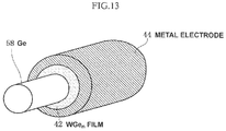
- FIG. 13 is a bird's eye view of main parts illustrating the source/drain region of a nano-wire type transistor according to the third embodiment.
- FIG. 14 is a diagram describing a relationship between a Ge/W composition ratio of the compound film of tungsten and germanium and an optical gap according to the third embodiment.
- FIG. 15 is a diagram describing a relationship between a composition ratio of a tungsten germanium cluster and a HOMO-LUMO gap.
- FIG. 16 is a diagram describing a relationship between a Ge/W composition ratio of a compound film of tungsten and germanium on a Ge substrate and a distance from the substrate according to the third embodiment.
- FIG. 17 is a diagram describing a relationship between an optical gap of the compound film of tungsten and germanium and a Schottky barrier height according to the third embodiment.
- FIG. 18 is a diagram describing a relationship between a Schottky barrier height formed on a contact interface between the compound film of tungsten and germanium and a Ge substrate, and specific contact resistance according to the third embodiment.
- Embodiments of the present invention relate to a compound film of tungsten and germanium having a germanium/tungsten composition ratio of 0.2 or more and less than 6.
- the compound film of the present embodiment includes an optical energy gap.
- the compound of tungsten and germanium having a germanium/tungsten composition ratio of 0.2 or more and less than 6 is described as a WGe n film (where, 0.2 ⁇ n ⁇ 6).
- the optical gap is 0.01 eV or more and 0.33 eV or less.
- ⁇ is an optical absorption coefficient
- E is photon energy
- E 0 is an optical energy gap
- A is a constant.
- photon energy dependency of the optical absorption coefficient is calculated from optical absorption measurement of the compound film, square roots (vertical axis) of the product of the optical absorption coefficient and the photon energy with respect to the photon energy (horizontal axis) are plotted and points of intersection of tangents and the horizontal axis of the plots are calculated as optical energy gaps.
- Such plots are called “Tauc plots” and the optical energy gap calculated in this way is also called a “Tauc gap” (see Non Patent Literature 5).
- the first method is one whereby a material gas of tungsten and a material gas of germanium are supplied, the material gases of tungsten and germanium are made to chemically react with each other in a gas phase to produce precursors, and the precursors are deposited on the substrate or below the metal electrode to produce a WGe n film.
- the second method is one whereby the material gas of tungsten and the material gas of germanium are supplied, the material gases of tungsten and germanium are made to chemically react with each other, not in a gas phase but on the substrate to produce a WGe n film.
- the first and second methods may be combined to cause the material gases of tungsten and germanium to chemically react with each other in the gas phase and on the substrate.
- the material gas of tungsten at least any one of a gas composed of fluorine and tungsten, a gas composed of chlorine and tungsten and a gas composed of an organic matter and tungsten may be preferably used.
- the material gas of germanium at least any one of monogermane composed of hydrogen and germanium, a gas composed of chlorine and germanium and a gas composed of an organic matter and germanium may be preferably used.
- the pressure of the germanium material gas within a range of 0.1 or more and 2000 Pa or less in the film forming chamber.
- the germanium material gas collide with the tungsten material gas in the gas phase to thereby undergo a chemical reaction, forming precursors of the WGe n film and repeating collision between the precursors and the germanium material gas, the Ge/W composition ratio of the precursors increases.
- An increase in the pressure of the germanium material gas causes the number of collisions between the germanium material gas and the precursors to increase, increasing chances the germanium material gas chemically reacts with the precursors and thereby increasing the Ge/W composition ratio of the precursor.
- the pressure of the germanium material gas and the Ge/W composition ratio n of the WGe n film there is a positive correlation between the pressure of the germanium material gas and the Ge/W composition ratio n of the WGe n film.
- a semiconductor such as Si or Ge, an insulator such as quartz, sapphire or resin, and a metal can be used for the substrate.
- a heating mechanism in one or more of an external wall, internal wall of the film forming chamber, a deposited substrate in the film forming chamber and a support mechanism of the deposited substrate.
- a structure with a heating mechanism attached to an internal wall or an external wall of the film forming chamber In order to heat the material gases, it is preferable to adopt a structure with the heating mechanism attached to the internal wall or the external wall of a gas introducing pipe.
- a structure with a heating mechanism attached to the deposited substrate for a chemical reaction to take place on the substrate.
- a method for manufacturing a tungsten germanium compound film will be described.
- WF 6 and GeH 4 are used as material gases.
- WF 6 When heated at a temperature lower than 120° C., WF 6 does not react with GeH 4 .
- GeH 4 molecules react with one another and an amorphous germanium film is formed.
- FIG. 1 is a schematic view illustrating a reaction process between GeH 4 and WF 6 .
- GeH 4 collides and reacts with WF 6 in the gas phase first (top left), then a precursor WGe n repeatedly collides with GeH 4 as shown by arrows sequentially, whereby Ge enrichment, that is, an increase in the n value advances. It is possible to promote reactions by providing assistance with thermal energy in collision.
- FIG. 2 is a schematic view illustrating a process of producing a thin film of a tungsten germanium compound having a Ge/W composition ratio of 6, on a substrate by aggregating precursors WGe 6 .
- the WGe n precursors synthesized in a gas phase are deposited on a substrate surface and a thin film of the tungsten germanium compound is deposited.
- the substrate is heated within a range of 120° C. or more and 270° C. or less, it is possible to promote the aggregation of the WGe n precursors.
- WF 6 and GeH 4 do not aggregate with each other well.
- GeH 4 molecules react with one another, forming an amorphous germanium film.
- the present manufacturing method is similar to the manufacturing method for the tungsten silicon compound film shown in Non Patent Literature 4, in that WF 6 is used as the material gas and thermal energy is used to cause a reaction between the material gases, whereas the present manufacturing method is different in that since it corresponds to manufacturing of a tungsten germanium compound film, it is different in use of GeH 4 as the material gas and in the range of manufacturing temperature.
- the present invention can produce the film at a temperature lower than that in the manufacturing method described in Non Patent Literature 4.
- the low-temperature process of the present invention is advantageous in securing performance of an electronic device when producing the electronic device.
- hydrogen or fluorine may be contained in the film formed as an impurity.
- the hydrogen or fluorine can be dissociated through heat treatment on the film.
- the dissociated substances can be identified through mass spectrometry of the dissociated substances from the film under heat treatment.
- FIG. 3 is a schematic view of a manufacturing apparatus according to the present embodiment.
- the manufacturing apparatus is provided with a film forming chamber 27 in which a material gas of tungsten reacts with a material gas of germanium, gas pipes 26 to introduce the material gas of tungsten and the material gas of germanium, a gas flow rate control mechanism such as a gas flow rate controller 25 to control the flow rate of at least one of the material gas of tungsten and the material gas of germanium, a gas pressure control mechanism (pressure gauge 32 , valve 30 ) to control pressures of the material gas of tungsten and the material gas of germanium, an exhaust mechanism (exhaust port 29 ) to exhaust the unreacted material gases of tungsten and germanium, a substrate 3 to deposit precursors in the film forming chamber 27 , and a substrate stage 31 with a heater to support and move the substrate.
- a gas flow rate control mechanism such as a gas flow rate controller 25 to control the flow rate of at least one of the material gas of tungsten and the material gas of german
- a heater 28 is disposed on the external wall of the film forming chamber 27 .
- the heater 28 has a function of heating a gas in the film forming chamber 27 .
- the heater With the heater disposed on the wall of the film forming chamber, it is possible to efficiently promote reactions in the gas phase in the embodiment in FIG. 1 .
- the WGe n precursors can be deposited on the substrate efficiently.
- By disposing a heating mechanism also on the substrate stage 31 it is possible to assist an increase in a gas temperature and promote germanium enrichment of the film.
- the manufacturing apparatus is provided with a plurality of gas bombs 24 to store material gases and an atmosphere gas (diluent gas) respectively, and the material gases and the atmosphere gas are introduced into the film forming chamber 27 via the gas pipes 26 , respectively.
- a plurality of gas bombs 24 to store material gases and an atmosphere gas (diluent gas) respectively, and the material gases and the atmosphere gas are introduced into the film forming chamber 27 via the gas pipes 26 , respectively.
- GeH 4 and WF 6 are used as the material gases.
- Chlorine-based gases such as Ge 2 H 6 or GeCl 4 may be used as the Ge material and a chloride-based gas such as WCl 6 can also be used as the W material.
- Ar or H 2 gas may also be used as the diluent gas.
- gases are supplied from the plurality of gas bombs (WF 6 , GeH 4 , Ar and H 2 from the left in FIG. 3 ).
- the flow rates of the gases introduced into the film forming chamber 27 are controlled.
- the pressure in the film forming chamber 27 is controlled by checking the pressure using the pressure gauge 32 disposed in the film forming chamber 27 and adjusting a diaphragm of the valve 30 disposed at the exhaust port 29 to exhaust the gas (indicated by an arrow in FIG. 3 ).
- the gas exhaust port 29 be sufficiently distanced from the gas inlet port and the film forming chamber have a sufficient capacity. Providing a large reaction space allows a sufficient gas phase reaction to take place in the film forming chamber.
- FIG. 4 is a cross-sectional schematic view of the film forming chamber of the manufacturing apparatus in FIG. 3 viewed from the gas inlet port side.
- the heater 28 is disposed on the external wall of the film forming chamber 27 , and disposing the substrate 3 in the center of the film forming chamber 27 makes it possible to uniformize a gas phase temperature and efficiently deposit the WGe n precursors on the substrate.
- the present embodiment will describe a case where the compound film is manufactured through only reactions on the substrate surface.
- FIG. 5 is a schematic view illustrating a reaction process between GeH 4 and WF 6 on the substrate surface.
- a thin film of a tungsten germanium compound can be produced without using any reaction in the gas phase according to the first embodiment.
- the substrate 3 is heated within a range of 120° C. or more and 270° C. or less using a heater 4 or the like, it is possible to prompt the aggregation of WGe n precursors.
- heating the substrate 3 at a temperature lower than 120° C. causes WF 6 and GeH 4 not to aggregate with each other well.
- heating the substrate 3 at a temperature higher than 270° C. causes GeH 4 molecules to react with one another, forming an amorphous germanium film.
- FIG. 6 is a schematic view of the manufacturing apparatus according to the present embodiment. Compared to the apparatus in FIG. 3 , the manufacturing apparatus in FIG. 6 is different in that no heater is disposed on the external wall of the film forming chamber. The heater is not disposed on the wall of the film forming chamber because the WGe n precursors are thereby deposited on the substrate efficiently and if the wall of the film forming chamber is heated by the heater, the WGe n precursors are deposited on the wall of the film forming chamber. The substrate 3 to deposit precursors and the substrate stage 31 with the heater are disposed in the film forming chamber 27 .
- the present embodiment will describe a structure in which a tungsten germanium compound film is applied to a semiconductor device with reference to the accompanying drawings.
- FIG. 7 is a cross-sectional schematic view of a semiconductor device in which the tungsten germanium compound film is used for an electrode structure.
- This is a stack structure in which the tungsten germanium compound is interposed in a contact interface between a semiconductor substrate and a metal electrode.
- the semiconductor device of the present embodiment has a structure including a WGe n film 42 which is a compound of tungsten and germanium on a semiconductor substrate 13 and a metal electrode 44 thereon.
- the stack structure according to the embodiment of the present invention makes it possible to reduce contact resistance between the metal electrode and the semiconductor substrate.
- FIG. 8 is a cross-sectional schematic view of a semiconductor device in which a tungsten germanium compound film with composition gradient is used for the electrode structure.
- a Ge substrate 33 is used for the semiconductor substrate and a W film 36 is used for the metal electrode in the embodiment in FIG. 7 , it is effective to cause the composition of the tungsten germanium compound to have a structure in which there is composition gradient from the substrate side in a stepwise manner in order of a WGe 2 film 34 and a WGe film 35 or in a continuous manner.
- FIG. 9 to FIG. 13 illustrate a structure peculiar to a semiconductor device using the WGe n film structure in FIGS. 1 and 2 .
- FIG. 9 is a cross-sectional schematic view of an N-MOS transistor.
- FIG. 9 has a source/drain structure with a WGe n film 42 inserted into a contact interface between a metal electrode 44 and a semiconductor substrate (N-type Si substrate 41 ).
- a central part in FIG. 9 is a gate structure with a gate insulating film 43 and a gate electrode (metal electrode 44 ) laminated on a P-type Si substrate 40 .
- WGe n film e.g., 0.2 ⁇ n ⁇ 6 having a high Ge composition ratio n makes it possible to reduce defect levels generated in the contact interface between the Si substrate and the WGe n film, control the height of the energy barrier generated between the metal and the Si substrate and reduce the contact resistance of the metal/Si substrate.
- the electrode structure provided with the WGe n film is effective not only for an N-MOS transistor but also for a P-MOS transistor or effective not only for a Si transistor but also for a Ge transistor.
- FIG. 10 is a cross-sectional schematic view of a non-junction type transistor having a source/drain structure using an SOI substrate.
- FIG. 10 is a cross-sectional schematic view of a non-junction type transistor having a source/drain structure in which the WGe n film 42 is inserted into a contact interface between the metal electrode 44 and a silicon on insulator (SOI) substrate 50 composed of Si and SiO 2 .
- SOI silicon on insulator
- Reducing the dopant concentration is particularly effective in reducing drain-induced barrier lowering (DIBL) which is one of short channel effects.
- DIBL drain-induced barrier lowering
- the contact resistance between the metal and the SOI substrate increases.
- FIG. 11 is a cross-sectional schematic view of a non-junction type transistor having a source/drain structure using a germanium on insulator (GOI) substrate instead of the SOI substrate in FIG. 10 .
- GOI germanium on insulator
- FIG. 12 is a bird's eye view of main parts illustrating a source/drain region of a stereoscopic transistor.
- a vertically standing stereoscopic Ge structure is formed in part of a Ge substrate 52 with an SiO 2 film 57 provided on a surface thereof and the WGe n film 42 is provided between the side face of the Ge structure and the stereoscopic metal electrode 44 . Since the WGe n film is formed through a gas phase reaction, the WGe n film has an excellent covering property and can be deposited on the stereoscopic structure uniformly.
- FIG. 13 is a bird's eye view of main parts illustrating the source/drain region of a nano-wire type transistor.
- an interposing layer made up of a WGe n film 42 is provided between a Ge wire 58 and a columnar metal electrode 44 surrounding the Ge wire 58 . Since the WGe n film 42 is formed through a gas phase reaction, it has an excellent covering property and can be deposited on the stereoscopic structure uniformly.
- FIG. 14 is a diagram describing a relationship between a Ge/W composition ratio of a tungsten germanium compound produced and an optical gap.
- the tungsten germanium compound film produced has (a Ge/W composition ratio of the tungsten germanium compound, the optical energy gap eV) of (1.01, 0.12) (1.49, 0.33) (1.80, 0.27) (2.60, 0.22) (3.11, 0.15) (3.97, 0.07) and (5.40, 0.09). It is apparent from FIG.
- the WGe n film (where, 0.2 ⁇ n ⁇ 6) has an optical energy gap, and the optical energy gap is 0.01 eV or more and 0.33 eV or less.
- the tungsten germanium compound film has metallic characteristics.
- the Ge/W composition ratio is 1 or more and 3.2 or less, the tungsten germanium compound film has an optical gap of 0.12 eV or more.
- the Ge/W composition ratio is 1.5, the optical gap exhibits a maximum value of 0.33 eV.
- the tungsten germanium compound film when the Ge/W composition ratio is 1.2 or more and 2.6 or less, the tungsten germanium compound film has an optical gap of 0.2 eV or more. Within a range where the Ge/W composition ratio is larger than 1.5, the optical gap decreases as the Ge/W composition ratio increases.
- FIG. 15 is a diagram describing values of a composition ratio of one tungsten germanium cluster and a HOMO-LUMO gap obtained through theoretical calculations (see Non Patent Literature 3).
- the results shown in FIG. 14 can be verified from FIG. 15 .
- the HOMO-LUMO gap decreases. This tendency coincides with the result that the optical gap decreases as the Ge/W composition ratio of the tungsten germanium compound described in FIG. 14 increases.
- the tungsten germanium compound film produced is constructed of a tungsten germanium cluster and the characteristics of the tungsten germanium compound film are determined by the characteristics of the tungsten germanium cluster.
- FIG. 16 is a diagram describing a relationship between the Ge/W composition ratio of the tungsten germanium compound film on a Ge substrate and a distance from the substrate regarding (1) (2) and (3) respectively.
- the composition ratio of the tungsten germanium compound film decreases as the distance from the substrate increases.
- the Ge/W composition ratio of the outermost surface of the tungsten germanium compound film which is farthest from the substrate is on the order of 0.5.
- Table 1 shows the relationship between the composition ratio of the tungsten germanium compound film in the substrate interface in FIG. 16 and the Schottky barrier height formed in the interface between the Ge substrate and the tungsten germanium compound film.
- the Schottky barrier height shows a small value of 0.46 eV.
- the Schottky barrier height shows a large value of 0.58 eV.
- the optical gap of the tungsten germanium compound film shows a value greater than 0.12 eV.
- the composition ratio is 0.5 or 3.3
- the optical gap shows a value smaller than 0.12 eV. Therefore, the composition ratio of the tungsten germanium compound in the substrate interface determines the Schottky barrier height formed in the interface between the Ge substrate and the tungsten germanium compound.
- FIG. 17 is a diagram illustrating a relationship between the optical gap of the tungsten germanium compound film and the Schottky barrier height formed in the interface between the Ge substrate and the tungsten germanium compound film.
- CNL denotes a charge neutral level of Ge.
- a junction of a conventional metal electrode and Ge shows the Schottky barrier height close to this CNL.
- the difference between white circle and black rectangle plots represent a difference in a production condition of the tungsten germanium compound film.
- the white circle indicates a flow rate of GeH 4 /WF 6 of 2/0.2 (SCCM) and the black rectangle indicates a flow rate of GeH 4 /WF 6 of 2/0.05 (SCCM).
- the Schottky barrier height decreases as the optical gap increases within a range of on the order of 0.12 eV or more or further a range of 0.2 eV or more. That is, FIG. 17 shows that the tungsten germanium compound film having a large optical gap is effective in achieving good junction characteristics.
- FIG. 18 is a diagram describing a relationship between a Schottky barrier height formed on a contact interface between the tungsten germanium compound film and the Ge substrate, and specific contact resistance.
- the contact resistance between the Ge substrate and the tungsten germanium compound film decreases as the height of the Schottky barrier decreases.
- This low contact resistance is effective for the semiconductor device shown in FIG. 9 to FIG. 13 to obtain excellent electric characteristics.
- the substrate is effective not only for Ge but also for Si or SiGe. This is because the mechanism whereby a Schottky barrier is formed in the interface between a group-IV semiconductor and a tungsten germanium compound film is the same.
- the film formed of the compound of tungsten and germanium of the present invention can realize a film having a desired optical energy gap according to a composition ratio, and is applicable to various types of semiconductor devices, and is industrially useful.
Landscapes
- Chemical & Material Sciences (AREA)
- Engineering & Computer Science (AREA)
- General Chemical & Material Sciences (AREA)
- Chemical Kinetics & Catalysis (AREA)
- Materials Engineering (AREA)
- Mechanical Engineering (AREA)
- Metallurgy (AREA)
- Organic Chemistry (AREA)
- Nanotechnology (AREA)
- Crystallography & Structural Chemistry (AREA)
- Mathematical Physics (AREA)
- Theoretical Computer Science (AREA)
- Physics & Mathematics (AREA)
- Electrodes Of Semiconductors (AREA)
- Chemical Vapour Deposition (AREA)
- Insulated Gate Type Field-Effect Transistor (AREA)
Abstract
Description
- Patent Literature 1: International Publication No. WO2009/107669
- Patent Literature 2: Japanese Patent Laid-Open No. 2011-66401
- Patent Literature 3: Japanese Patent Laid-Open No. 2014-067804
- Non Patent Literature 1: Journal of Vacuum Science & Technology A 24, 474 (2006),
- Non Patent Literature 2: Applied Surface Science 73,82 (1993).
- Non Patent Literature 3: The Journal of Physical Chemistry A 110, 12670 (2006),
- Non Patent Literature 4: The Journal of Chemical Physics 144, 084703 (2016),
- Non Patent Literature 5: Materials Research Bulletin 5, 721(1970).
(αE)1/2 =A(E−E 0) (Equation 1)
| TABLE 1 | ||
| Ge/W | ||
| composition ratio of | Schottkey | |
| WGen film in | barrier height | |
| Number | substrate interface | (eV) |
| — | 0 | 0.58 |
| — | 0.5 | 0.58 |
| (1) | 1.9 | 0.46 |
| (2) | 2.4 | 0.46 |
| (3) | 3.3 | 0.58 |
- 1 WGen precursor
- 2, 42 WGen film
- 3 Substrate
- 4, 28 Heater
- 11 WGe6 precursor
- 12 WGe6 film
- 13 Semiconductor substrate
- 24 Gas bomb
- 25 Gas flow rate controller
- 26 Gas pipe
- 27 Film forming chamber
- 29 Exhaust port
- 30 Valve
- 31 Substrate stage
- 32 Pressure gauge
- 33, 52 Ge substrate
- 34 WGe2 film
- 35 WGe film
- 36 W film
- 40 P-type Si substrate
- 41 N-type Si substrate
- 43 Gate insulating film
- 44 Metal electrode
- 50 SOI substrate
- 51 GOI substrate
- 57 SiO2 film
- 58 Ge
Claims (19)
Applications Claiming Priority (3)
| Application Number | Priority Date | Filing Date | Title |
|---|---|---|---|
| JP2016-120390 | 2016-06-17 | ||
| JP2016120390 | 2016-06-17 | ||
| PCT/JP2017/022205 WO2017217512A1 (en) | 2016-06-17 | 2017-06-15 | Compound film of tungsten and germanium, and semiconductor device |
Publications (2)
| Publication Number | Publication Date |
|---|---|
| US20190207007A1 US20190207007A1 (en) | 2019-07-04 |
| US10692986B2 true US10692986B2 (en) | 2020-06-23 |
Family
ID=60664016
Family Applications (1)
| Application Number | Title | Priority Date | Filing Date |
|---|---|---|---|
| US16/302,441 Active US10692986B2 (en) | 2016-06-17 | 2017-06-15 | Compound film of tungsten and germanium, and semiconductor device |
Country Status (5)
| Country | Link |
|---|---|
| US (1) | US10692986B2 (en) |
| EP (1) | EP3474315B1 (en) |
| JP (1) | JP6896291B2 (en) |
| KR (1) | KR102383369B1 (en) |
| WO (1) | WO2017217512A1 (en) |
Families Citing this family (1)
| Publication number | Priority date | Publication date | Assignee | Title |
|---|---|---|---|---|
| US11631811B2 (en) * | 2021-05-07 | 2023-04-18 | Micron Technology, Inc. | WSiGe electrode structures for memory devices, and associated devices and systems |
Citations (13)
| Publication number | Priority date | Publication date | Assignee | Title |
|---|---|---|---|---|
| JPH03126836A (en) | 1989-10-11 | 1991-05-30 | Hitachi Ltd | Superconducting material |
| US5162246A (en) | 1990-04-27 | 1992-11-10 | North Carolina State University | Selective germanium deposition on silicon and resulting structures |
| JPH04334019A (en) | 1991-05-09 | 1992-11-20 | Hitachi Ltd | Manufacture of compound semiconductor device |
| US5391394A (en) * | 1990-01-08 | 1995-02-21 | Lsi Logic Corporation | Tungsten deposition process for low contact resistivity to silicon |
| US5731245A (en) * | 1994-08-05 | 1998-03-24 | International Business Machines Corp. | High aspect ratio low resistivity lines/vias with a tungsten-germanium alloy hard cap |
| JPH11340116A (en) | 1998-05-22 | 1999-12-10 | Nec Corp | X-ray mask, method of manufacturing the same, semiconductor device and method of manufacturing the same |
| JP2002038258A (en) | 2000-07-21 | 2002-02-06 | Toshiba Corp | Sputtering target |
| US20080274598A1 (en) | 2007-03-19 | 2008-11-06 | Texas Instruments Inc. | Doped WGe to form dual metal gates |
| WO2009107669A1 (en) | 2008-02-28 | 2009-09-03 | 独立行政法人産業技術総合研究所 | Thin film of metal silicon compound and process for producing the thin film of metal silicon compound |
| US20100060126A1 (en) * | 2008-09-09 | 2010-03-11 | Canon Kabushiki Kaisha | Electron source and image display apparatus |
| JP2011066401A (en) | 2009-08-21 | 2011-03-31 | National Institute Of Advanced Industrial Science & Technology | Thin film transistor |
| JP2014067804A (en) | 2012-09-25 | 2014-04-17 | Sharp Corp | Photoelectric conversion element |
| WO2015174240A1 (en) | 2014-05-12 | 2015-11-19 | 国立研究開発法人産業技術総合研究所 | Crystalline alignment layer laminate structure, electronic memory, and method for manufacturing crystalline alignment layer laminate structure |
Family Cites Families (2)
| Publication number | Priority date | Publication date | Assignee | Title |
|---|---|---|---|---|
| KR100621532B1 (en) * | 2003-01-22 | 2006-09-14 | 캐논 가부시끼가이샤 | Sintered body and film forming method using the same |
| KR20090107669A (en) | 2008-04-10 | 2009-10-14 | 주식회사 비즈모델라인 | Call taxi operation method and call taxi terminal and recording medium for the same |
-
2017
- 2017-06-15 US US16/302,441 patent/US10692986B2/en active Active
- 2017-06-15 KR KR1020187031963A patent/KR102383369B1/en active Active
- 2017-06-15 JP JP2018524013A patent/JP6896291B2/en active Active
- 2017-06-15 WO PCT/JP2017/022205 patent/WO2017217512A1/en not_active Ceased
- 2017-06-15 EP EP17813406.0A patent/EP3474315B1/en active Active
Patent Citations (13)
| Publication number | Priority date | Publication date | Assignee | Title |
|---|---|---|---|---|
| JPH03126836A (en) | 1989-10-11 | 1991-05-30 | Hitachi Ltd | Superconducting material |
| US5391394A (en) * | 1990-01-08 | 1995-02-21 | Lsi Logic Corporation | Tungsten deposition process for low contact resistivity to silicon |
| US5162246A (en) | 1990-04-27 | 1992-11-10 | North Carolina State University | Selective germanium deposition on silicon and resulting structures |
| JPH04334019A (en) | 1991-05-09 | 1992-11-20 | Hitachi Ltd | Manufacture of compound semiconductor device |
| US5731245A (en) * | 1994-08-05 | 1998-03-24 | International Business Machines Corp. | High aspect ratio low resistivity lines/vias with a tungsten-germanium alloy hard cap |
| JPH11340116A (en) | 1998-05-22 | 1999-12-10 | Nec Corp | X-ray mask, method of manufacturing the same, semiconductor device and method of manufacturing the same |
| JP2002038258A (en) | 2000-07-21 | 2002-02-06 | Toshiba Corp | Sputtering target |
| US20080274598A1 (en) | 2007-03-19 | 2008-11-06 | Texas Instruments Inc. | Doped WGe to form dual metal gates |
| WO2009107669A1 (en) | 2008-02-28 | 2009-09-03 | 独立行政法人産業技術総合研究所 | Thin film of metal silicon compound and process for producing the thin film of metal silicon compound |
| US20100060126A1 (en) * | 2008-09-09 | 2010-03-11 | Canon Kabushiki Kaisha | Electron source and image display apparatus |
| JP2011066401A (en) | 2009-08-21 | 2011-03-31 | National Institute Of Advanced Industrial Science & Technology | Thin film transistor |
| JP2014067804A (en) | 2012-09-25 | 2014-04-17 | Sharp Corp | Photoelectric conversion element |
| WO2015174240A1 (en) | 2014-05-12 | 2015-11-19 | 国立研究開発法人産業技術総合研究所 | Crystalline alignment layer laminate structure, electronic memory, and method for manufacturing crystalline alignment layer laminate structure |
Non-Patent Citations (8)
| Title |
|---|
| Extended European Search Report dated Jan. 2, 2020 in corresponding European Patent Application No. 17813406.0. |
| Gaudet et al., "Thin film reaction of transition metals with germanium", J. Vac. Sci. Technol. A 24(3), May/Jun. 2006, pp. 474-485. |
| International Search Report dated Sep. 5, 2017 in corresponding International Application No. PCT/JP2017/022205. |
| Mutsaers et al., "Reduction of WF6 using GeH4", Applied Surface Science 73 (1993) 82-85. |
| Okada et al., "Si-rich W silicide films composed of W-atom-encapsulated Si clusters deposited using gas-phase reactions of WF6 with SiH4" The Journal of Chemical Physics 144, 084703 (2016). |
| Tauc, "Absorption Edge and Internal Electric Fields in Amorphous Semiconductors", Mat. Res. Bull. vol. 5, pp. 721-730, 1970. |
| Wang et al., "Geometries and Electronic Properties of the Tungsten-Doped Germanium Clusters: WGen(n=1-17)", J. Phys. Chem. A2006, 110, (2006) 12670-12677. |
| Written Opinion of the International Searching Authority dated Sep. 5, 2017 in corresponding International Application No. PCT/JP2017/022205. |
Also Published As
| Publication number | Publication date |
|---|---|
| EP3474315A1 (en) | 2019-04-24 |
| WO2017217512A1 (en) | 2017-12-21 |
| JPWO2017217512A1 (en) | 2019-04-11 |
| EP3474315B1 (en) | 2021-12-22 |
| KR20190019914A (en) | 2019-02-27 |
| EP3474315A4 (en) | 2020-01-22 |
| JP6896291B2 (en) | 2021-06-30 |
| KR102383369B1 (en) | 2022-04-05 |
| US20190207007A1 (en) | 2019-07-04 |
Similar Documents
| Publication | Publication Date | Title |
|---|---|---|
| TWI509699B (en) | Strain source of engineering strain on the channel | |
| US20240312786A1 (en) | Contact Structures With Deposited Silicide Layers | |
| KR101728377B1 (en) | Doped semiconductor films and processing | |
| TWI430335B (en) | Method for selectively depositing an epitaxial layer | |
| US9218973B2 (en) | Methods of doping substrates with ALD | |
| TWI742680B (en) | Semiconductor structures and methods for formng the same | |
| US20120199887A1 (en) | Methods of controlling tungsten film properties | |
| CN109427547A (en) | For depositing doped germanium tin method for semiconductor and related semiconductor device structure | |
| US20210367063A1 (en) | Semiconductor Device and Method of Manufacture | |
| TWI524392B (en) | Stabilized deuterated metal film and method of manufacturing same | |
| US20220336637A1 (en) | Semiconductor Device and Method of Manufacture | |
| TW202108815A (en) | Methods for depositing a molybdenum nitride film on a surface of a substrate by a cyclical deposition process and related semiconductor device structures including a molybdenum nitride film | |
| JP5018473B2 (en) | Manufacturing method of semiconductor device | |
| JP6503543B2 (en) | Transition metal silicide film, method and apparatus for manufacturing the same, and semiconductor device | |
| US20170352738A1 (en) | Contact formation on germanium-containing substrates using hydrogenated silicon | |
| TW202201531A (en) | Integrated circuit and method of fabricating the same | |
| US10692986B2 (en) | Compound film of tungsten and germanium, and semiconductor device | |
| TWI484556B (en) | Method for forming a high growth rate low resistivity tantalum film on a tantalum substrate (2) | |
| KR102948022B1 (en) | Method and apparatus for forming ruthenium silicide film on surface of substrate | |
| US20230163197A1 (en) | Semiconductor Device and Method of Manufacture | |
| TW201829819A (en) | Methods and materials for CMOS contacts and barrier layers | |
| US20080145978A1 (en) | Deposition of silicon germanium nitrogen precursors for strain engineering | |
| US20260052739A1 (en) | Semiconductor device and method for fabricating the same | |
| CN102479717A (en) | Method for forming silicon-germanium epitaxial layer | |
| CN120077763A (en) | Low Wen Gongliu epitaxial deposition process |
Legal Events
| Date | Code | Title | Description |
|---|---|---|---|
| FEPP | Fee payment procedure |
Free format text: ENTITY STATUS SET TO UNDISCOUNTED (ORIGINAL EVENT CODE: BIG.); ENTITY STATUS OF PATENT OWNER: LARGE ENTITY |
|
| AS | Assignment |
Owner name: NATIONAL INSTITUTE OF ADVANCED INDUSTRIAL SCIENCE Free format text: ASSIGNMENT OF ASSIGNORS INTEREST;ASSIGNORS:OKADA, NAOYA;UCHIDA, NORIYUKI;KANAYAMA, TOSHIHIKO;REEL/FRAME:047642/0741 Effective date: 20181122 Owner name: NATIONAL INSTITUTE OF ADVANCED INDUSTRIAL SCIENCE AND TECHNOLOGY, JAPAN Free format text: ASSIGNMENT OF ASSIGNORS INTEREST;ASSIGNORS:OKADA, NAOYA;UCHIDA, NORIYUKI;KANAYAMA, TOSHIHIKO;REEL/FRAME:047642/0741 Effective date: 20181122 |
|
| STPP | Information on status: patent application and granting procedure in general |
Free format text: DOCKETED NEW CASE - READY FOR EXAMINATION |
|
| STPP | Information on status: patent application and granting procedure in general |
Free format text: NON FINAL ACTION MAILED |
|
| STPP | Information on status: patent application and granting procedure in general |
Free format text: RESPONSE TO NON-FINAL OFFICE ACTION ENTERED AND FORWARDED TO EXAMINER |
|
| STPP | Information on status: patent application and granting procedure in general |
Free format text: PUBLICATIONS -- ISSUE FEE PAYMENT VERIFIED |
|
| STCF | Information on status: patent grant |
Free format text: PATENTED CASE |
|
| CC | Certificate of correction | ||
| MAFP | Maintenance fee payment |
Free format text: PAYMENT OF MAINTENANCE FEE, 4TH YEAR, LARGE ENTITY (ORIGINAL EVENT CODE: M1551); ENTITY STATUS OF PATENT OWNER: LARGE ENTITY Year of fee payment: 4 |